

NSC DS14C238WMX, DS14C238WM Datasheet
DS14C238
Single Supply TIA/EIA-2324x4Driver/Receiver
DS14C238 Single Supply TIA/EIA-2324x4Driver/Receiver
May 1999
General Description
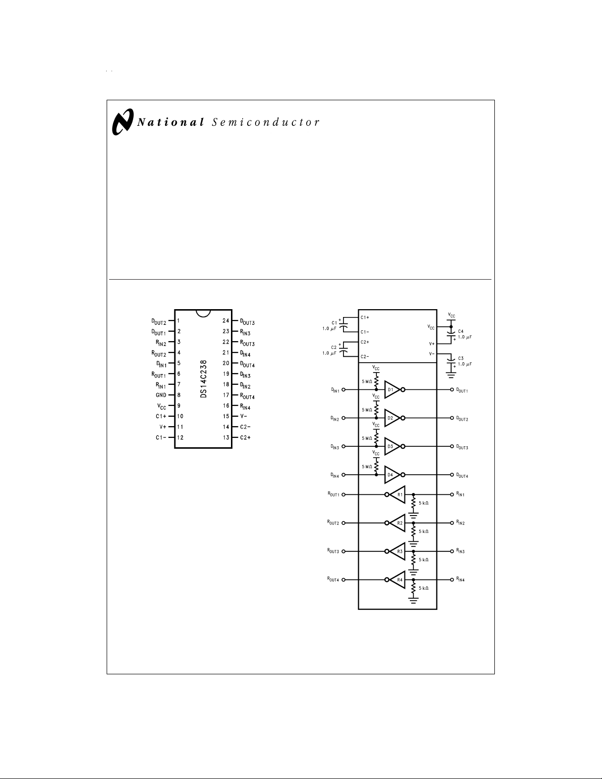
The DS14C238 is a four driver, four receiver device which
conforms to the TIA/EIA-232-E standard and CCITT V.28
recommendations. This device eliminates
employing an internal DC-DCconverter to generate the necessary output levels from a single +5V supply. Driver slew
rate control and receiver noise filtering have also been internalized to eliminate the need for external slew rate control
and noise filtering capacitors.
±
12V supplies by
Features
n Conforms to TIA/EIA-232-E and CCITT V.28
n Internal DC-DC converter
n Operates with single +5V supply
n Low power requirement—I
n Internal driver slew rate control
n Receiver noise filtering
n Operates above 120 kbits/sec
n Direct replacement for MAX238
CC
Connection Diagram Functional Diagram
DS011282-1
Order Number DS14C238WM
See NS Package Number M24B
10 mA max
DS011282-2
© 1999 National Semiconductor Corporation DS011282 www.national.com
Absolute Maximum Ratings (Note 1)
If Military/Aerospace specified devices are required,
please contact the National Semiconductor Sales Office/
Distributors for availability and specifications.
Supply Voltage (V
V+ Pin (V
V− Pin +0.3V to −15V
Driver Input Voltage −0.3V to (V
Driver Output Voltage (V+ +0.3V) to (V−
Receiver Input Voltage
Receiver Output Voltage −0.3V to (V
Junction Temperature +150˚C
Maximum Package Power Dissipation
) −0.3V to +6V
CC
−0.3V) to +15V
CC
@
+25˚C (Note 6)
CC
CC
+0.3V)
−0.3V)
±
30V
+0.3V)
Lead Temp.
(Soldering, 4 Seconds) +260˚C
Short Circuit Duration
) Continuous
(D
OUT
ESD Rating
(HBM, 1.5 kΩ, 100 pF) ≥ 2.0 kV
Recommended Operating
Conditions
Min Max Units
Supply Voltage, V
Operating Free Air Temp. (T
DS14C238 0 +70 ˚C
4.5 5.5 V
CC
)
A
WM Package 1400 mW
Storage Temp. Range −65˚C to +150˚C
Electrical Characteristics (Note 2)
Over recommended operating conditions, unless otherwise specified.
Symbol Parameter Conditions Min Typ Max Units
DEVICE CHARACTERISTICS
V+ Positive Power Supply R
V− Negative Power Supply R
I
CC
Supply Current (VCC) No Load 7.0 10 mA
DRIVER CHARACTERISTICS
V
IH
V
IL
I
IH
I
IL
V
OH
V
OL
I
OS
High Level Input Voltage 2.0 V
Low Level Input Voltage GND 0.8 V
High Level Input Current VIN≥ 2.0V −10 +10 µA
Low Level Input Current VIN≤ 0.8V −10 +10 µA
High Level Output Voltage RL=3kΩ 5.0 7.4 V
Low Level Output Voltage −6.3 −5.0 V
+ Output High Short VO= 0V, VIN= 0.8V (Note 3) −30 −15 −5.0 mA
Circuit Current
I
− Output Low Short VO= 0V, VIN= 2.0V 5.0 12 30 mA
OS
Circuit Current
R
O
Output Resistance −2V ≤ VO≤ +2V, VCC= GND = 0V 300 Ω
RECEIVER CHARACTERISTICS
V
TH
V
TL
V
HY
R
IN
I
IN
V
OH
V
OL
Input High Threshold
Voltage
Input Low Threshold
Voltage
Hysteresis 0.2 0.4 1.0 V
Input Resistance 3.0 4.5 7.0 kΩ
Input Current VIN= +15V 2.14 3.8 5.0 mA
High Level Output Voltage VIN= −3V, IO= −3.2 mA 3.5 4.5 V
Low Level Output Voltage VIN= +3V, IO= +2.0 mA 0.25 0.4 V
=3kΩ, C1–C4 = 1.0 µF, DIN= 0.8V 9.0 V
L
=3kΩ, C1–C4 = 1.0 µF, DIN= 2.0V −8.0 V
L
CC
1.9 2.4 V
0.8 1.5 V
V
= +3V 0.43 0.6 +1.0 mA
IN
V
= −3V −1.0 −0.6 −0.43 mA
IN
V
= −15V −5.0 −3.8 −2.14 mA
IN
V
= −3V, IO= −20 µA 4.0 4.9 V
IN
V
www.national.com 2
 Loading...