

DS14C232
Low Power +5V Powered TIA/EIA-232 Dual
Driver/Receiver
General Description
The DS14C232 is a low power dual driver/receiver featuring
an onboard DC to DC converter, eliminating the need for
±
12V power supplies.The device only requires a +5V power
supply. I
CC
is specified at 3.0 mA maximum, making the device ideal for battery and power conscious applications. The
drivers’ slew rate is set internally and the receivers feature
internal noise filtering, eliminating the need for external slew
rate and filter capacitors. The device is designed to interface
data terminal equipment (DTE) with data circuit-terminating
equipment (DCE).The driver inputs and receiver outputs are
TTL and CMOS compatible. DS14C232C driver outputs and
receiver inputs meet TIA/EIA-232-E (RS-232) and CCITT
V.28 standards.
Features
n Pin compatible with industry standard MAX232, LT1081,
ICL232 and TSC232
n Single +5V power supply
n Low power — I
CC
3.0 mA maximum
n DS14C232C meets TIA/EIA-232-E (RS-232) and CCITT
V.28 standards
n CMOS technology
n Receiver Noise Filter
n Package efficiency — 2 drivers and 2 receivers
n Available in Plastic DIP, Narrow and Wide SOIC
packages
n TIA/EIA-232 compatible extended temperature range
option:
DS14C232T −40˚C to +85˚C
DS14C232E/J: −55˚C to +125˚C
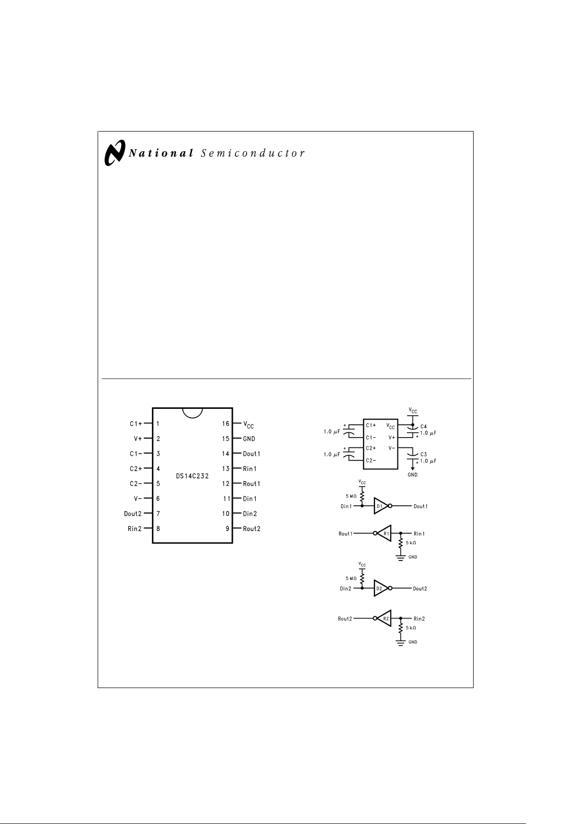
Connection Diagram Functional Diagram
DS010744-1
Order Number DS14C232CN, DS14C232CM, or
DS14C232TM
See NS Package Number N16E, or M16A
DS010744-2
October 1999
DS14C232 Low Power +5V Powered TIA/EIA-232 Dual Driver/Receiver
© 1999 National Semiconductor Corporation DS010744 www.national.com
Absolute Maximum Ratings (Note 1)
Specifications for the 883 version of this product are
listed separately on the following pages.
Supply Voltage, V
CC
−0.3V to 6V
V
+
Pin (VCC− 0.3)V to +14V
V
−
Pin +0.3V to −14V
Driver Input Voltage −0.3V to (V
CC
+ 0.3V)
Driver Output Voltage (V
+
+ 0.3V) to (V−−
0.3V)
Receiver Input Voltage
±
25V
Receiver Output Voltage −0.3V to (V
CC
+ 0.3V)
Junction Temperature +150˚C
Maximum Package Power Dissipation
@
25˚C (Note 6)
N Package 1698 mW
M Package 1156 mW
Short Circuit Duration,
D
OUT
Continuous
Storage Temp. Range −65˚C to +150˚C
Lead Temp. (Soldering, 4
sec.) +260˚C
ESD Rating
(HBM, 1.5 kΩ, 100 pF) ≥ 2.5 kV
Recommended Operating
Conditions
Min Max Units
Supply Voltage, V
CC
4.5 5.5 V
Operating Free Air Temp. (T
A
)
DS14C232C 0 +70 ˚C
DS14C232T −40 +85 ˚C
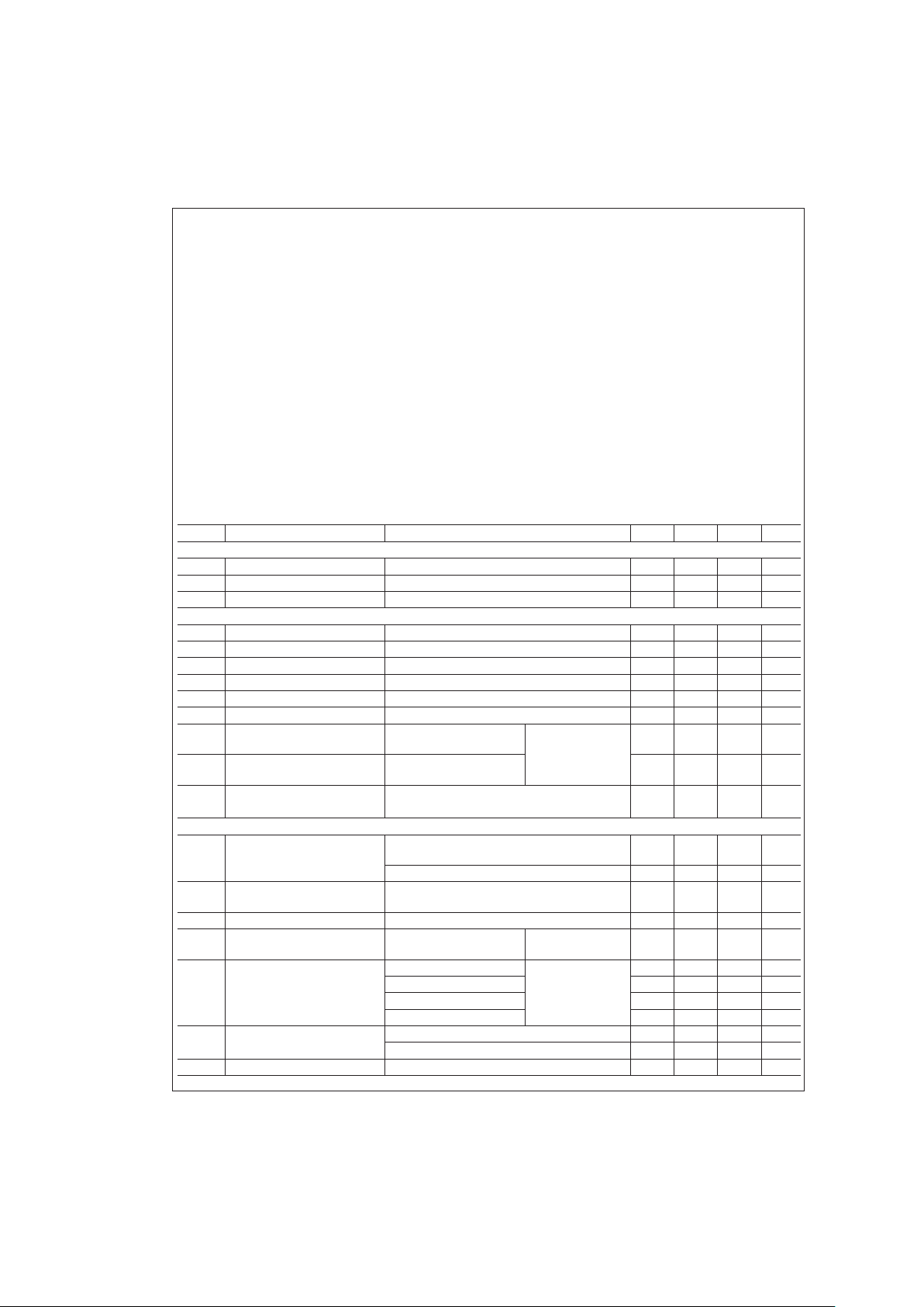
Electrical Characteristics (Note 2)
Over recommended operating conditions, unless otherwise specified
Symbol Parameter Conditions Min Typ Max Units
DC TO DC CONVERTER CHARACTERISTICS
V
+
Positive Power Supply R
L
=
3kΩ,C1–C4=1.0 µF, D
IN
=
0.8V 9.0 V
V
−
Negative Power Supply R
L
=
3kΩ,C1–C4=1.0 µF, D
IN
=
2.0V −8.5 V
I
CC
Supply (VCC) Current No Load 1.0 3.0 mA
DRIVER CHARACTERISTICS
V
IH
High Level Input Voltage 2 V
CC
V
V
IL
Low Level Input Voltage GND 0.8 V
I
IH
High Level Input Current VIN≥ 2.0V −10 +10 µA
I
IL
Low Level Input Current VIN≤ 0.8V −10 +10 µA
V
OH
High Level Output Voltage R
L
=
3kΩ 5.0 8.0 V
V
OL
Low Level Output Voltage R
L
=
3kΩ −7.0 −5.0 V
I
OS+
Output High Short Circuit
Current
V
O
=
0V, V
IN
=
0.8V (Note 3) −30 −15 −5.0 mA
I
OS−
Output Low Short Circuit
Current
V
O
=
0V, V
IN
=
2V 5.0 11 30 mA
R
O
Output Resistance −2V ≤ VO≤ +2V, 300 Ω
V
CC
=0V=
GND
RECEIVER CHARACTERISTICS
V
TH
Input High Threshold
Voltage
V
CC
=
5.0V 1.9 2.4 V
V
CC
=
5.0V
±
10
%
1.9 2.6 V
V
TL
Input Low Threshold
Voltage
0.8 1.5 V
V
HY
Hysteresis 0.2 0.4 1.0 V
R
IN
Input Resistance −15V ≤ VIN≤
+15V
3.0 4.7 7.0 kΩ
I
IN
Input Current V
IN
=
+15V +2.14 +3.75 +5.0 mA
V
IN
=
+3V +0.43 +0.64 +1.0 mA
V
IN
=
−3V −1.0 −0.64 −0.43 mA
V
IN
=
−15V −5.0 −3.75 −2.14 mA
V
OH
High Level Output Voltage V
IN
=
−3V, I
O
=
−3.2 mA 3.5 4.5 V
V
IN
=
−3V, I
O
=
−20 µA 4.0 4.9 V
V
OL
Low Level Output Voltage V
IN
=
+3V, I
O
=
+3.2 mA 0.15 0.4 V
DS14C232
www.national.com 2
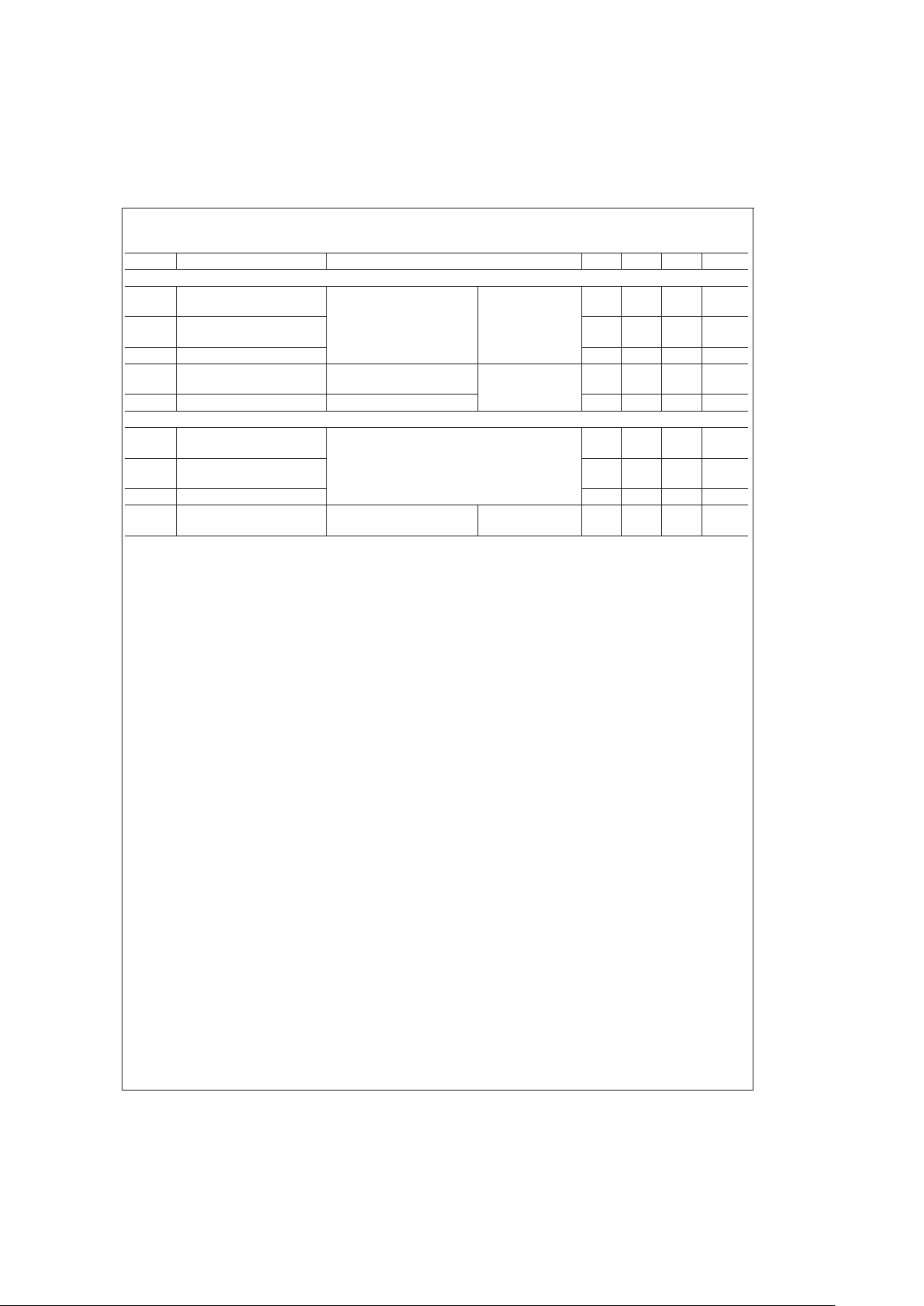
Switching Characteristics
Over recommended operating conditions, unless otherwise specified.
Symbol Parameter Conditions Min Typ Max Units
DRIVER CHARACTERISTICS
t
PLH
Propagation Delay Low to
High
R
L
=
3kΩ
C
L
=
50 pF
Figure 1
and
Figure 2
1.0 4.0 µs
t
PHL
Propagation Delay High to
Low
1.0 4.0 µs
t
SK
Skew |t
PLH−tPHL
| 0.1 1.0 µs
SR1 Output Slew Rate R
L
=
3kΩto7kΩ,C
L
=
50 pF
(Note 7) 4.0 30 V/µs
SR2 Output Slew Rate R
L
=
3kΩ,C
L
=
2500 pF 4.5 V/µs
RECEIVER CHARACTERISTICS
t
PLH
Propagation Delay Low to
High
Input Pulse Width>10 µs 2.9 6.5 µs
t
PHL
Propagation Delay High to
Low
C
L
=
50 pF 2.5 6.5 µs
t
SK
Skew |t
PLH−tPHL
|(
Figures 3, 4
) 0.4 2.0 µs
t
nw
Noise Pulse Width
Rejected
(
Figures 3, 4
) 0.7 0.5 µs
Note 1: “Absolute Maximum Ratings” are those values beyond which the safety of the device cannot be guaranteed. They are not meant to imply that the devices
should be operated at these limits. The tables of “Electrical Characteristics” specify conditions for device operation.
Note 2: Currentinto device pins is defined as positive. Current outof device pins is definedas negative. All voltages are referencedto ground unless otherwise specified.
Note 3: IOS
+
and IOS−values are for one output at a time. If more than one output is shorted simultaneously, the device power dissipation may be exceeded.
Note 4: Receiver AC input waveform for test purposes: t
r
=
t
f
=
200 ns, V
IH
=
3V, V
IL
=
−3V, f=30 kHz.
Note 5: All typicals are given for V
CC
=
5.0V.
Note 6: Ratings apply to ambient temperature at +25˚C. Above this temperature derate: N Package 15.6 mW/˚C, and M Package 10.6 mW/˚C.
Note 7: Slew rate is defined as ∆V/∆t, measured between
±
3V level.
DS14C232
www.national.com3
Absolute Maximum Ratings (Note 1)
For complete Military Product Specifications, refer to
the appropriate SMD or MDS.
Supply Voltage, V
CC
−0.3V to 6V
V
+
Pin (VCC− 0.3)V to +14V
V
−
Pin +0.3V to −14V
Driver Input Voltage −0.3V to (V
CC
+ 0.3V)
Driver Output Voltage (V
+
+ 0.3V) to (V−− 0.3V)
Receiver Input Voltage
±
25V
Receiver Output Voltage −0.3V to (V
CC
+ 0.3V)
Maximum Package Power Dissipation
@
25˚C (Note 8)
J Package 1520 mW
E Package 2000 mW
Short Circuit Duration, D
OUT
Continuous
Storage Temp. Range −65˚C to +150˚C
Lead Temp. (Soldering, 4 sec.) +260˚C
ESD Rating
(HMB, 1.5 kΩ, 100 pF) ≥ 2.5 kV
Recommended Operating
Conditions
Min Max Units
Supply Voltage, V
CC
4.5 5.5 V
Operating Free Air Temp. (T
A
)
DS14C232E/J −55 +125 ˚C
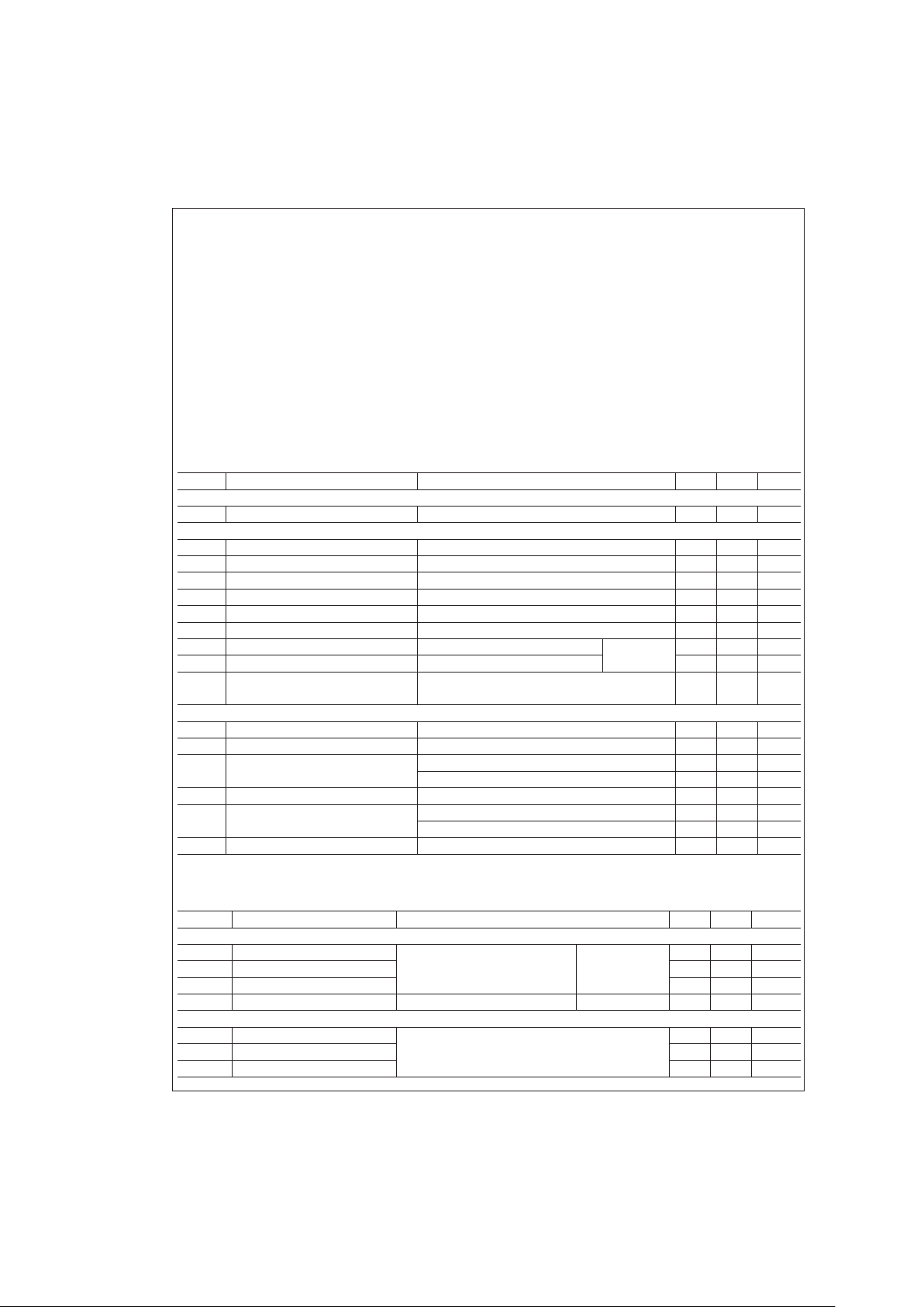
Electrical Characteristics (Note 2)
Over recommended operating conditions, unless otherwise specified
Symbol Parameter Conditions Min Max Units
DEVICE CHARACTERISTICS (C1–C4=1.0 µF)
I
CC
Supply (VCC) Current No Load 8.0 mA
DRIVER CHARACTERISTICS
V
IH
High Level Input Voltage 2V
V
IL
Low Level Input Voltage 0.8 V
I
IH
High Level Input Current VIN≥ 2.0V 100 µA
I
IL
Low Level Input Current V
IN
=
0V 100 µA
V
OH
High Level Output Voltage R
L
=
3kΩ 5.0 V
V
OL
Low Level Output Voltage R
L
=
3kΩ −5.0 V
I
OS+
Output High Short Circuit Current V
O
=
0V (Note 3) −25 mA
I
OS−
Output Low Short Circuit Current V
O
=
0V 25 mA
R
O
Output Resistance −2V ≤ VO≤ +2V, T
A
=
25˚C, 300 Ω
V
CC
=0V=
GND
RECEIVER CHARACTERISTICS (C1–C4=1.0 µF)
V
TH
Input High Threshold Voltage 3.0 V
V
TL
Input Low Threshold Voltage 0.2 V
V
HY
Hysteresis T
A
=
25˚C, +125˚C 0.1 1.0 V
T
A
=
−55˚C 0.05 1.0 V
R
IN
Input Resistance V
IN
=
±
3V and±15V, T
A
=
25˚C 3.0 7.0 kΩ
V
OH
High Level Output Voltage I
O
=
−3.2 mA 3.5 V
I
O
=
−20 µA 4.0 V
V
OL
Low Level Output Voltage I
O
=
+3.2 mA 0.4 V
Switching Characteristics
Over recommended operating conditions, unless otherwise specified.
Symbol Parameter Conditions Min Max Units
DRIVER CHARACTERISTICS (C1–C4=1.0 µF)
t
PLH
Propagation Delay Low to High R
L
=
3kΩ,C
L
=
50 pF
Figures 1, 2
4.0 µs
t
PHL
Propagation Delay High to Low 4.0 µs
t
SK
Skew |t
PLH−tPHL
| 1.0 µs
SR1 Output Slew Rate R
L
=
3kΩto7kΩ,C
L
=
2500 pF (Note 7) 1.5 30 V/µs
RECEIVER CHARACTERISTICS (C1–C4=1.0 µF)
t
PLH
Propagation Delay Low to High Input Pulse Width>10 µs 8.0 µs
t
PHL
Propagation Delay High to Low C
L
=
50 pF 8.0 µs
t
SK
Skew |t
PLH−tPHL
|(
Figures 3, 4
) 2.0 µs
DS14C232
www.national.com 4

Switching Characteristics (Continued)
Note 8: Ratings apply to ambient temperature at +25˚C. Above this temperature derate: J Package 12.2 mW/˚C and E Package 13.3 mW/˚C.
Connection Diagrams
Parameter Measurement Information
J Package
16-Lead Dual-In-line Package
DS010744-1
E Package
20-Lead Ceramic Leadless Chip Carrier
DS010744-10
For Complete Military Product Specifications
See MDS or SMD.
Order Number DS14C232J/883 or DS14C232E/883
See NS Package Number E20A or J16A
DS010744-3
FIGURE 1. Driver Load Circuit
DS010744-4
FIGURE 2. Driver Switching Waveform
DS14C232
www.national.com5

Parameter Measurement Information (Continued)
Pin Descriptions
VCC(Pin 16)
Power supply pin for the device, +5V (
±
10%).
V+ (Pin 2)
Positive supply for TIA/EIA-232-E drivers. Recommended
external capacitor: C4-1.0 µF (6.3V). Capacitor value should
be larger than 1 µF. This supply is not intended to be loaded
externally.
V− (Pin 6)
Negative supply for TIA/EIA-232-E drivers. Recommended
external capacitor: C3-1.0 µF (16V). Capacitor value should
be larger than 1 µF. This supply is not intended to be loaded
externally.
C1+, C1− (Pins 1, 3)
External capacitor connection pins. Recommended capacitor: 1.0 µF (6.3V). Capacitor value should be larger than
1µF.
C2+, C2− (Pins 4, 5)
External capacitor connection pins. Recommended capacitor: 1.0 µF (16V). Capacitor value should be greater than
1µF.
D
IN
1, DIN2 (Pins 11, 10)
Driver input pins are TTL/CMOS compatible. Inputs of unused drivers may be left open, an internal active pull-up resistor (500 kΩ minimum, typically 5 MΩ) pulls input HIGH.
Output will be LOW for open inputs.
D
OUT
1, D
OUT
2 (Pins 14, 7)
Driver output pins conform to TIA/EIA-232-E levels.
R
IN
1, RIN2 (Pins 13, 8)
Receiver input pins accept TIA/EIA-232-E input voltages
(
±
25V). Receivers feature a noise filter and guaranteed hysteresis of 100 mV. Unused receiver input pins may be left
open. Internal input resistor 4.7 kΩ pulls input low, providing
a failsafe high output.
R
OUT
1, R
OUT
2 (Pins 12, 9)
Receiver output pins are TTL/CMOS compatible. Receiver
output HIGH voltage is specified for both CMOS and TTL
load conditions.
GND (Pin 15)
Ground Pin.
DS010744-5
FIGURE 3. Receiver Load Circuit
DS010744-6
FIGURE 4. Receiver Propagation Delays and Noise Rejection (Note 4)
DS14C232
www.national.com 6

Typical Application Information
Typical Connection Diagram
Application of DS14C232 and INS8250
DS010744-7
DS010744-9
DS14C232
www.national.com7

Typical Performance Characteristics
DRIVER VOH&VOLvs
POWER SUPPLY VOLTAGE
DS010744-11
DS010744-12
V
CC
=
5.0V, R
L
=
3kΩ,C
L
=
15 pF (includes jig and probe capacitance), C
P
=
1µF
DS010744-13
S1 V
O
2.0V V
OL
0.8V V
OH
DS14C232
www.national.com 8

Typical Performance Characteristics (Continued)
DRIVER SLEW RATE vs POWER
SUPPLY VOLTAGE & LOAD
CAPACITANCE
DS010744-14
DS010744-15
T
a
=
25˚C, R
L
=
5kΩ,C
P
=
1µF,ƒ=30 KHz
DS010744-16
SR=6V/t1 or 6V/t2, whichever is greater.
DS14C232
www.national.com9

Physical Dimensions inches (millimeters) unless otherwise noted
Order Number DS14C232E/883
NS Package Number E20A
Order Number DS14C232J/883
NS Package Number J16A
DS14C232
www.national.com 10

Physical Dimensions inches (millimeters) unless otherwise noted (Continued)
Order Number DS14C232CM or DS14C232TM
NS Package Number M16A
Order Number DS14C232CN
NS Package Number N16E
DS14C232
www.national.com11

Notes
LIFE SUPPORT POLICY
NATIONAL’S PRODUCTS ARE NOT AUTHORIZED FOR USE AS CRITICAL COMPONENTS IN LIFE SUPPORT
DEVICES OR SYSTEMS WITHOUT THE EXPRESS WRITTEN APPROVAL OF THE PRESIDENT AND GENERAL
COUNSEL OF NATIONAL SEMICONDUCTOR CORPORATION. As used herein:
1. Life support devices or systems are devices or
systems which, (a) are intended for surgical implant
into the body, or (b) support or sustain life, and
whose failure to perform when properly used in
accordance with instructions for use provided in the
labeling, can be reasonably expected to result in a
significant injury to the user.
2. A critical component is any component of a life
support device or system whose failure to perform
can be reasonably expected to cause the failure of
the life support device or system, or to affect its
safety or effectiveness.
National Semiconductor
Corporation
Americas
Tel: 1-800-272-9959
Fax: 1-800-737-7018
Email: support@nsc.com
National Semiconductor
Europe
Fax: +49 (0) 1 80-530 85 86
Email: europe.support@nsc.com
Deutsch Tel: +49 (0) 1 80-530 85 85
English Tel: +49 (0) 1 80-532 78 32
Français Tel: +49 (0) 1 80-532 93 58
Italiano Tel: +49 (0) 1 80-534 16 80
National Semiconductor
Asia Pacific Customer
Response Group
Tel: 65-2544466
Fax: 65-2504466
Email: sea.support@nsc.com
National Semiconductor
Japan Ltd.
Tel: 81-3-5639-7560
Fax: 81-3-5639-7507
www.national.com
DS14C232 Low Power +5V Powered TIA/EIA-232 Dual Driver/Receiver
National does not assume any responsibility for use of any circuitry described, no circuit patent licenses are implied and National reserves the right at any time without notice to change said circuitry and specifications.
 Loading...