

NSC DS1488N, DS1488MX, DS1488M Datasheet
DS1488
Quad Line Driver
General Description
The DS1488 is a quad line driver which converts standard
TTL input logic levels through one stage of inversion to output levels which meet EIA Standard RS-232D and CCITT
Recommendation V.24.
Features
n Current limited output:±10 mA typ
n Power-off source impedance: 300Ω min
n Simple slew rate control with external capacitor
n Flexible operating supply range
n Inputs are TTL/LS compatible
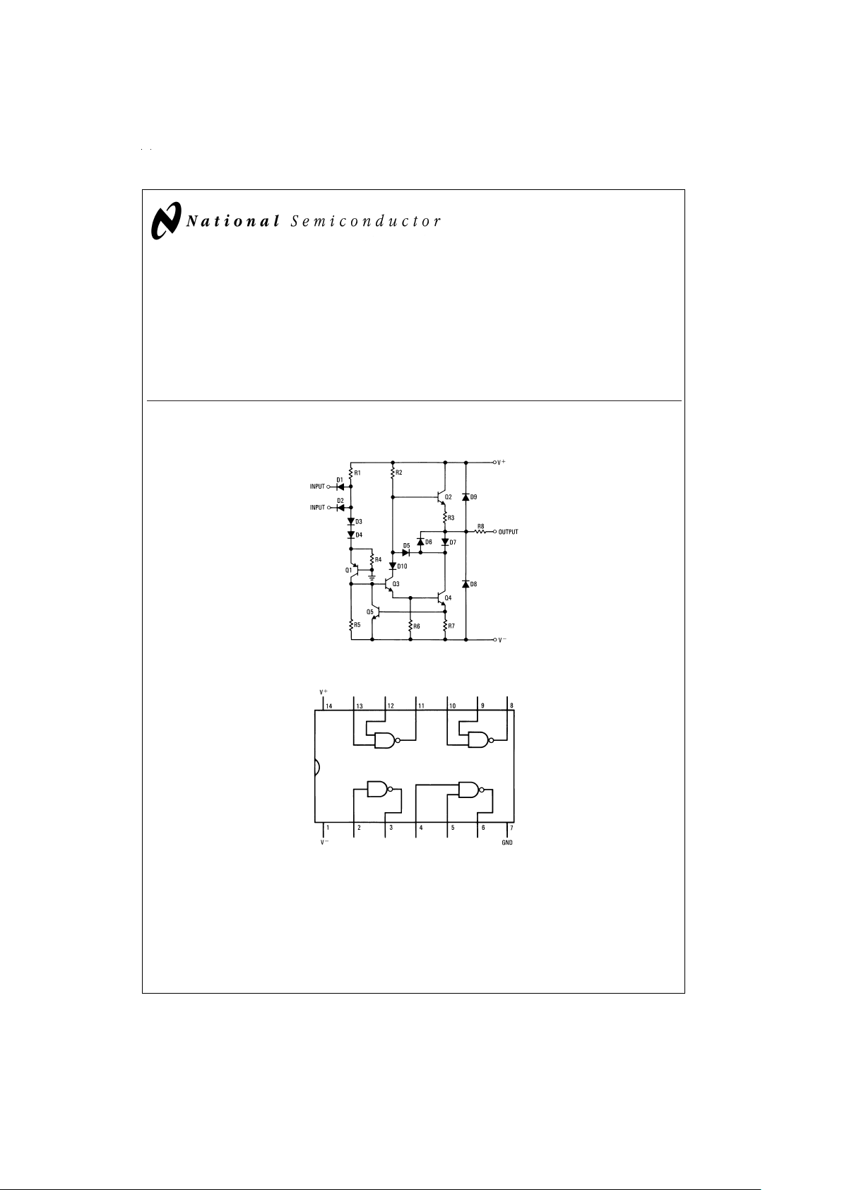
Schematic and Connection Diagrams
1/4 Circuit
DS005776-1
Dual-In-Line Package
DS005776-2
Top View
Order Number DS1488M or DS1488N
See NS Package Number M14A or N14A
July 1999
DS1488 Quad Line Driver
© 1999 National Semiconductor Corporation DS005776 www.national.com
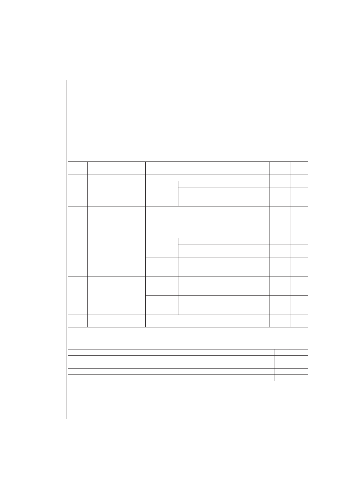
Absolute Maximum Ratings (Note 2)
If Military/Aerospace specified devices are required,
please contact theNational Semiconductor Sales Office/
Distributors for availability and specifications.
Supply Voltage
V
+
+15V
V
−
−15V
Input Voltage (V
IN
) −15V ≤ VIN≤
7.0V
Output Voltage
±
15V
Operating Temperature Range 0˚C to +75˚C
Storage Temperature Range −65˚C to +150˚C
Maximum Power Dissipation (Note 1) at 25˚C
Molded DIP Package 1280 mW
SO Package 974 mW
Lead Temperature (Soldering, 4
sec.) 260˚C
Note 1: Derate molded DIP package 10.2 mW/˚C above 25˚C; derate SO
package 7.8 mW/˚C above 25˚C.
Electrical Characteristics (Notes 3, 4)
VCC+=9V, VCC−=−9V unless otherwise specified
Symbol Parameter Conditions Min Typ Max Units
I
IL
Logical “0” Input Current V
IN
=
0V −0.8 −1.3 mA
I
IH
Logical “1” Input Current V
IN
=
+5.0V 0.005 10.0 µA
V
OH
High Level Output Voltage R
L
=
3.0 kΩ,V
+
=
9.0V, V
−
=
−9.0V 6.0 7.1 V
V
IN
=
0.8V V
+
=
13.2V, V
−
=
−13.2V 9.0 10.7 V
V
OL
Low Level Output Voltage R
L
=
3.0 kΩ,V
+
=
9.0V, V
−
=
−9.0V −6.0 7.0 V
V
IN
=
1.9V V
+
=
13.2V, V
−
=
−13.2V −9.0 −10.6 V
I
OS
+ High Level Output V
OUT
=
0V, V
IN
=
0.8V −6.0 −10.0 −12.0 mA
Short-Circuit Current
I
OS
− Low Level Output V
OUT
=
0V, V
IN
=
1.9V 6.0 10.0 12.0 mA
Short-Circuit Current
R
OUT
Output Resistance V
+
=
V
−
=
0V, V
OUT
=
±
2V 300 Ω
I
CC
+ Positive Supply Current V
IN
=
1.9V V
+
=
9.0V, V
−
=
−9.0V 11.6 20.0 mA
(Output Open) V
+
=
12V, V
−
=
−12V 15.7 25.0 mA
V
+
=
15V, V
−
=
−15V 19.4 34.0 mA
V
IN
=
0.8V V
+
=
9.0V, V
−
=
−9.0V 3.4 6.0 mA
V
+
=
12V, V
−
=
−12V 4.1 7.0 mA
V
+
=
15V, V
−
=
−15V 9.1 12.0 mA
I
CC
− Negative Supply Current V
IN
=
1.9V V
+
=
9.0V, V
−
=
−9.0V −10.8 −17.0 mA
(Output Open) V
+
=
12V, V
−
=
−12V −14.6 −23.0 mA
V
+
=
15V, V
−
=
−15V −18.3 −34.0 mA
V
IN
=
0.8V V
+
=
9.0V, V
−
=
−9.0V −0.001 −0.100 mA
V
+
=
12V, V
−
=
−12V −0.001 −0.100 mA
V
+
=
15V, V
−
=
−15V −0.01 −2.5 mA
P
d
Power Dissipation V
+
=
9.0V, V
−
=
−9.0V 252 333 mW
V
+
=
12V, V
−
=
−12V 444 576 mW
Switching Characteristics
(V
CC
=
9V, V
EE
=
−9V, T
A
=
25˚C)
Symbol Parameter Conditions Min Typ Max Units
t
pd1
Propagation Delay to a Logical “1” R
L
=
3.0 kΩ,C
L
=
15 pF, T
A
=
25˚C 187 350 ns
t
pd0
Propagation Delay to a Logical “0” R
L
=
3.0 kΩ,C
L
=
15 pF, T
A
=
25˚C 45 175 ns
t
r
Rise Time R
L
=
3.0 kΩ,C
L
=
15 pF, T
A
=
25˚C 63 100 ns
t
f
Fall Time R
L
=
3.0 kΩ,C
L
=
15 pF, T
A
=
25˚C 33 75 ns
Note 2: “AbsoluteMaximum Ratings” are those values beyond which the safety of the device cannot be guaranteed. Except for “Operating TemperatureRange” they
are not meant to imply that the devices should be operated at these limits. The table of “Electrical Characteristics” provides conditions for actual device operation.
Note 3: Unless otherwise specified min/max limits apply across the 0˚C to +75˚C temperature range for the DS1488.
Note 4: All currents into device pins shown as positive, out of device pins as negative, all voltages referenced to ground unless otherwise noted. All values shown
as max or min on absolute value basis.
www.national.com 2
 Loading...