

NSC DP8431VX-33, DP8431V-33 Datasheet
TL/F/11118
DP8430V/31V/32V-33 microCMOS Programmable
256k/1M/4M Dynamic RAM Controller/Drivers
July 1993
DP8430V/31V/32V-33 microCMOS Programmable
256k/1M/4M Dynamic RAM Controller/Drivers
General Description
The DP8430V/31V/32V dynamic RAM controllers provide a
low cost, single chip interface between dynamic RAM and
all 8-, 16- and 32-bit systems. The DP8430V/31V/32V generate all the required access control signal timing for
DRAMs. An on-chip refresh request clock is used to automatically refresh the DRAM array. Refreshes and accesses
are arbitrated on chip. If necessary, a WAIT
or DTACK output inserts wait states into system access cycles, including
burst mode accesses. RAS
low time during refreshes and
RAS
precharge time after refreshes and back to back accesses are guaranteed through the insertion of wait states.
Separate on-chip precharge counters for each RAS
output
can be used for memory interleaving to avoid delayed back
to back accesses because of precharge. An additional feature of the DP8432V is two access ports to simplify dual
accessing. Arbitration among these ports and refresh is
done on chip.
Features
Y
On chip high precision delay line to guarantee critical
DRAM access timing parameters
Y
microCMOS process for low power
Y
High capacitance drivers for RAS, CAS,WEand DRAM
address on chip
Y
On chip support for nibble, page and static column
DRAMs
Y
Byte enable signals on chip allow byte writing in a word
size up to 32 bits with no external logic
Y
Can use a single clock source. Up to 33 MHz operating
frequency
Y
On board Port A/Port B (DP8432V only)/refresh arbitration logic
Y
Direct interface to all major microprocessors
Y
4 RAS and 4 CAS drivers (the RAS and CAS configuration is programmable)
Ý
of Pins
Ý
of Address
Largest Direct Drive Access
Control
(PLCC) Outputs
DRAM Memory Ports
Possible Capacity Available
DP8430V 68 9 256 kbit 4 Mbytes Single Access Port
DP8431V 68 10 1 Mbit 16 Mbytes Single Access Port
DP8432V 84 11 4 Mbit 64 Mbytes Dual Access Ports (A and B)
Block Diagram
DP8430V/31V/32V DRAM Controller
TL/F/11118– 1
FIGURE 1
TRI-STATEÉis a registered trademark of National Semiconductor Corporation.
Staggered Refresh
TM
is a trademark of National Semiconductor Corporation.
C
1995 National Semiconductor Corporation RRD-B30M75/Printed in U. S. A.

Table of Contents
1.0 INTRODUCTION
2.0 SIGNAL DESCRIPTIONS
2.1 Address, R/W and Programming Signals
2.2 DRAM Control Signals
2.3 Refresh Signals
2.4 Port A Access Signals
2.5 Port B Access Signals (DP8432V)
2.6 Common Dual Port Signals (DP8432V)
2.7 Power Signals and Capacitor Input
2.8 Clock Inputs
3.0 PROGRAMMING AND RESETTING
3.1 Reset
3.2 Programming Methods
3.2.1 Mode Load Only Programming
3.2.2 Chip Selected Access Programming
3.3 Internal Programming Modes
4.0 PORT A ACCESS MODES
4.1 Access Mode 0
4.2 Access Mode 1
4.3 Extending CAS with Either Access Mode
4.4 Read-Modify-Write Cycles with Either Access Mode
4.5 Additional Access Support Features
4.5.1 Address Latches and Column Increment
4.5.2 Address Pipelining
4.5.3 Delay CAS
During Write Accesses
5.0 REFRESH OPTIONS
5.1 Refresh Control Modes
5.1.1 Automatic Internal Refresh
5.1.2 Externally Controlled Refresh
5.2 Refresh Cycle Types
5.2.1 Conventional Refresh
5.2.2 Staggered Refresh
TM
5.2.3 Error Scrubbing Refresh
5.3 Extending Refresh
6.0 PORT A WAIT STATE SUPPORT
6.1 WAIT
Type Output
6.2 DTACK
Type Output
6.3 Dynamically Increasing the Number of Wait States
6.4 Guaranteeing RAS
Low Time and RAS Precharge
Time
7.0 RAS
AND CAS CONFIGURATION MODES
7.1 Byte Writing
7.2 Memory Interleaving
7.3 Address Pipelining
7.4 Error Scrubbing
7.5 Page/Burst Mode
8.0 TEST MODE
9.0 DRAM CRITICAL TIMING PARAMETERS
9.1 Programmable Values of t
RAH
and t
ASC
9.2 Calculation of t
RAH
and t
ASC
10.0 DUAL ACCESSING (DP8432V)
10.1 Port B Access Mode
10.2 Port B Wait State Support
10.3 Common Port A and Port B Dual Port Functions
10.3.1 GRANTB Output
10.3.2 LOCK
Input
11.0 ABSOLUTE MAXIMUM RATINGS
12.0 DC ELECTRICAL CHARACTERISTICS
13.0 AC TIMING PARAMETERS
14.0 DP8430V/31V/32V USER HINTS
2

1.0 Introduction
The DP8430V/31V/32V DRAM controllers are the latest
devices based upon the DP8420A/21A/22A predecessors.
The DP8430V/31V/32V implement changes which do not
allow them to be pin compatible with any of the DP842XA or
the DP842XV DRAM controllers. Two changes have been
made: The limits for the input frequency to DELCLK have
been increased making possible the use of a single clock
source. A RESET input is now available making the reset
procedure easier. These changes, although minimal, facilitate the use of the controllers and make them even more
attractive for high performance applications. The controllers
incorporate address latches, refresh counter, row/column/
refresh address multiplexer, delay line, refresh/access/precharge arbitration logic and high capacitive drivers. The
DP8430V/31V/32V DRAM controllers allow any manufacturer’s CPU or bus to directly interface to DRAM arrays up to
64 Mbytes in size.
Reset:
The user must reset the controller before programming it.
Reset is achieved by asserting the RESET
input for at least
16 positive edges of clock.
Programming:
After reset, the user can program the controller by either
one of two methods: Mode Load Only Programming or Chip
Select Access Programming. The chip is programmed
through the address bus.
Initialization Period:
Once the DP8430V/31V/32V has been programmed for the
first time, a 60 ms initialization period is entered. During this
time the DRC performs refreshes to the DRAM array so
further warm up cycles are unnecessary. The initialization
period is entered only after the first programming after a
reset.
Accessing Modes:
After resetting and programming the chip, the DP8430V/
31V/32V is ready to access the DRAM. There are two
modes of accessing with these controllers. Mode 0, which
indicates RAS
synchronously and Mode 1, which indicates
RAS
asynchronously.
Refresh Modes:
Two refresh modes can be programmed. The user can
choose Automatic Internal Refresh or Externally Controlled
Refresh. With any refresh mode the user can perform burst
refreshes.
Refresh Types:
There are three types of refreshing available: Conventional,
Staggered and Error Scrubbing. Any refresh control mode
can be used with any type of refresh.
Wait Support:
The DP8430V/31V/32V have wait support available as
DTACK
or WAIT. Both are programmable. DTACK, Data
Transfer ACKnowledge, is useful for processors whose wait
signal is active high. WAIT
is useful for those processors
whose wait signal is active low. The user can choose either
at programming. These signals are used by the on chip arbiter to insert wait states to guarantee the arbitration between
accesses, refreshes and precharge. Both signals are independent of the access mode chosen and both signals can
be dynamically delayed further through the WAITIN
signal to
the DP8430V/31V/32V.
Sequential Accesses (Static Column/Page Mode):
The DP8430V/31V/32V have address latches, used to
latch the bank, row and column address inputs. Once the
address is latched, a COLumn INCrement (COLINC) feature
can be used to increment the column address. The address
latches can also be programmed to be fall through. COLINC
can be used for Sequential Accesses of Static Column
DRAMs. Also, COLINC in conjunction with ECAS
inputs can
be used for Sequential Accesses to Page Mode DRAMs.
RAS
and CAS Configuration (Byte Writing):
The RAS and CAS drivers can be configured to drive a one,
two or four bank memory array up to 32 bits in width. The
ECAS
signals can then be used to select one of four CAS
drivers for Byte Writing with no extra logic.
Memory Interleaving:
When configuring the DP8430V/31V/32V for more than
one bank, Memory Interleaving can be used. By tying the
low order address bits to the bank select lines B0 and B1,
sequential back to back accesses will not be delayed since
these controllers have separate precharge counters per
bank.
Address Pipelining:
The DP8430V/31V/32V are capable of performing Address
Pipelining. In address pipelining, the DRC will guarantee the
column address hold time and switch the internal multiplexor to place the row address on the address bus. At this
time, another memory access to another bank can be initiated.
Dual Accessing:
Finally, the DP8432V has all the features previously mentioned and unlike the DP8430V/31V, the DP8432V has a
second port to allow a second CPU to access the same
memory array. The DP8432V has four signals to support
Dual Accessing, these signals are AREQB
, ATACKB, LOCK
and GRANTB. All arbitration for the two ports and refresh is
done on chip by the controller through the insertion of wait
states. Since the DP8432V has only one input address bus,
the address lines must be multiplexed externally. The signal
GRANTB can be used for this purpose.
Terminology:
The following explains the terminology used in this data
sheet. The terms negated and asserted are used. Asserted
refers to a ‘‘true’’ signal. Thus, ‘‘ECAS0
asserted’’ means
the ECAS0
input is at a logic 0. The term ‘‘COLINC asserted’’ means the COLINC input is at a logic 1. The term negated refers to a ‘‘false’’ signal. Thus, ‘‘ECAS0
negated’’
means the ECAS0
input is at a logic 1. The term ‘‘COLINC
negated’’ means the input COLINC is at a logic 0. The table
shown below clarifies this terminology.
Signal Action Logic Level
Active High Asserted High
Active High Negated Low
Active Low Asserted Low
Active Low Negated High
3
Connection Diagrams
TL/F/11118– 2
Top View
FIGURE 2
Order Number DP8430V-33
See NS Package Number V68A
TL/F/11118– 3
Top View
FIGURE 3
Order Number DP8431V-33
See NS Package Number V68A
TL/F/11118– 4
Top View
FIGURE 4
Order Number DP8432V-33
See NS Package Number V84A
4
2.0 Signal Descriptions
Pin Device (If not Input/
Description
Name Applicable to All) Output
2.1 ADDRESS, R/W AND PROGRAMMING SIGNALS
R0–10 DP8432V I ROW ADDRESS: These inputs are used to specify the row address during an access
to the DRAM. They are also used to program the chip when ML
is asserted (except
R0–9 DP8430V/31V I
R10).
C0–10 DP8432V I COLUMN ADDRESS: These inputs are used to specify the column address during an
access to the DRAM. They are also used to program the chip when ML
is asserted
C0–9 DP8430V/31V I
(except C10).
B0, B1 I BANK SELECT: Depending on programming, these inputs are used to select a group
of RAS and CAS outputs to assert during an access. They are also used to program
the chip when ML
is asserted.
ECAS0–3 I ENABLE CAS: These inputs are used to enable a single or group of CAS outputs
when asserted. In combination with the B0, B1 and the programming bits, these
inputs select which CAS
output or CAS outputs will assert during an access. The
ECAS
signals can also be used to toggle a group of CAS outputs for page/nibble
mode accesses. They also can be used for byte write operations. If ECAS
0is
negated during programming, continuing to assert the ECAS
0 while negating AREQ
or AREQB during an access, will cause the CAS outputs to be extended while the
RAS
outputs are negated (the ECASn inputs have no effect during scrubbing
refreshes).
RESET I RESET: At power up, this input is used to reset the DRAM controller. The user must
keep RESET
low for at least 16 positive edges of clock. After programming this input
must remain negated (high) to avoid an unwanted reset.
WIN I WRITE ENABLE IN: This input is used to signify a write operation to the DRAM. If
ECAS0 is asserted during programming, the WE output will follow this input. This
input asserted will also cause CAS
to delay to the next positive clock edge if address
bit C9 is asserted during programming.
COLINC I COLUMN INCREMENT: When the address latches are used, and RFIP is negated,
this input functions as COLINC. Asserting this signal causes the column address to
(EXTNDRF) I
be incremented by one. When RFIP
is asserted, this signal is used to extend the
refresh cycle by any number of periods of CLK until it is negated.
ML I MODE LOAD: This input signal, when low, enables the internal programming register
that stores the programming information.
2.2 DRAM CONTROL SIGNALS
Q0–10 DP8432V O DRAM ADDRESS: These outputs are the multiplexed output of the R0 –9, 10 and
C0–9, 10 and form the DRAM address bus. These outputs contain the refresh
Q0–9 DP8431V O
address whenever RFIP
is asserted. They contain high capacitive drivers with 20X
Q0–8 DP8430V O
series damping resistors.
RAS0–3 O ROW ADDRESS STROBES: These outputs are asserted to latch the row address
contained on the outputs Q0–8, 9, 10 into the DRAM. When RFIP
is asserted, the
RAS
outputs are used to latch the refresh row address contained on the Q0–8, 9, 10
outputs in the DRAM. These outputs contain high capacitive drivers with 20X series
damping resistors.
CAS0–3 O COLUMN ADDRESS STROBES: These outputs are asserted to latch the column
address contained on the outputs Q0–8, 9, 10 into the DRAM. These outputs have
high capacitive drivers with 20X series damping resistors.
WE O WRITE ENABLE or REFRESH REQUEST: This output asserted specifies a write
operation to the DRAM. When negated, this output specifies a read operation to the
(RFRQ
)O
DRAM. When the DP8430V/31V/32V is programmed in address pipelining mode or
when ECAS0 is negated during programming, this output will function as RFRQ.
RFRQ
asserted, specifies that 13 msor15ms have passed. RFRQ can be used to
externally request a refresh through the input RFSH
. This output has a high
capacitive driver and a 20X series damping resistor.
5
2.0 Signal Descriptions (Continued)
Pin Device (If not Input/
Description
Name Applicable to All) Output
2.3 REFRESH SIGNALS
RFIP O REFRESH IN PROGRESS: This output is asserted prior to a refresh cycle and is
negated when all the RAS
outputs are negated for that refresh.
RFSH I REFRESH: This input asserted will request a refresh. If this input is continually
asserted, the DP8430V/31V/32V will perform refresh cycles in a burst refresh
fashion until the input is negated.
2.4 PORT A ACCESS SIGNALS
ADS I ADDRESS STROBE or ADDRESS LATCH ENABLE: Depending on programming,
this input can function as ADS
or ALE. In mode 0, the input functions as ALE and
(ALE) I
when asserted along with CS
causes an internal latch to be set. Once this latch is set
an access will start from the positive clock edge of CLK as soon as possible. In Mode
1, the input functions as ADS
and when asserted along with CS, causes the access
RAS
to assert if no other event is taking place. If an event is taking place, RAS will be
asserted from the positive edge of CLK as soon as possible. In both cases, the low
going edge of this signal latches the bank, row and column address if programmed to
do so.
CS I CHIP SELECT: This input signal must be asserted to enable a Port A access.
AREQ I ACCESS REQUEST: This input signal in Mode 0 must be asserted some time after
the first positive clock edge after ALE has been asserted. When this signal is
negated, RAS
is negated for the access. In Mode 1, this signal must be asserted
before ADS
can be negated. When this signal is negated, RAS is negated for the
access.
WAIT O WAIT or DTACK: This output can be programmed to insert wait states into a CPU
access cycle. With R7 negated during programming, the output will function as a
(DTACK
)O
WAIT
type output. In this case, the output will be active low to signal a wait condition.
With R7 asserted during programming, the output will function as DTACK
. In this
case, the output will be negated to signify a wait condition and will be asserted to
signify the access has taken place. Each of these signals can be delayed by a
number of positive clock edges or negative clock levels of CLK to increase the
microprocessor’s access cycle through the insertion of wait states.
WAITIN I WAIT INCREASE: This input can be used to dynamically increase the number of
positive clock edges of CLK until DTACK
will be asserted or WAIT will be negated
during a DRAM access.
2.5 PORT B ACCESS SIGNALS
AREQB DP8432V I PORT B ACCESS REQUEST: This input asserted will latch the row, column and bank
address if programmed, and requests an access to take place for Port B. If the
only
access can take place, RAS
will assert immediately. If the access has to be delayed,
RAS
will assert as soon as possible from a positive edge of CLK.
ATACKB DP8432V O ADVANCED TRANSFER ACKNOWLEDGE PORT B: This output is asserted when
the access RAS
is asserted for a Port B access. This signal can be used to generate
only
the appropriate DTACK
or WAIT type signal for Port B’s CPU or bus.
6
2.0 Signal Descriptions (Continued)
Pin Device (If not Input/
Description
Name Applicable to All) Output
2.6 COMMON DUAL PORT SIGNALS
GRANTB DP8432V O GRANT B: This output indicates which port is currently granted access to the DRAM
array. When GRANTB is asserted, Port B has access to the array. When GRANTB is
only
negated, Port A has access to the DRAM array. This signal is used to multiplex the
signals R0–8, 9, 10; C0 –8, 9, 10; B0 – 1; WIN
; LOCK and ECAS0 – 3 to the DP8432V
when using dual accessing.
LOCK DP8432V I LOCK: This input can be used by the currently granted port to ‘‘lock out’’ the other
port from the DRAM array by inserting wait states into the locked out port’s access
only
cycle until LOCK is negated.
2.7 POWER SIGNALS AND CAPACITOR INPUT
V
CC
I POWER: Supply Voltage.
GND I GROUND: Supply Voltage Reference.
CAP I CAPACITOR: This input is used by the internal PLL for stabilization. The value of the
ceramic capacitor should be 0.1 mF and should be connected between this input and
ground.
2.8 CLOCK INPUTS
There are two clock inputs to the DP8430V/31V/32V, CLK and DELCLK. These two clocks may both be tied to the same clock
input, or they may be two separate clocks, running at different frequencies, asynchronous to each other.
CLK I SYSTEM CLOCK: This input may be in the range of 0 Hz up to 25 MHz. This input is
generally a constant frequency but it may be controlled externally to change
frequencies or perhaps be stopped for some arbitrary period of time.
This input provides the clock to the internal state machine that arbitrates between
accesses and refreshes. This clock’s positive edges and negative levels are used to
extend the WAIT
(DTACK) signals. Ths clock is also used as the reference for the
RAS
precharge time and RAS low time during refresh.
All Port A and Port B accesses are assumed to be synchronous to the system clock
CLK.
DELCLK I DELAY LINE CLOCK: The input frequency to DELCLK should be in the range of
12 MHz to 40 MHz. This frequency will be internally divided by choosing a divisor
when programming the part. The result of the division should be a frequency of
2 MHz. This is because the Phase Lock Loop that generates the delay line assumes
an input clock frequency of 2 MHz. If after dividing DELCLK by one of the internal
divisors (6, 8, 10, 12, 14, 16, 18 or 20) the resulting frequency is not 2 MHz, the delay
line will suffer.
For example, if the DELCLK frequency is 18 MHz and a divide by 8 is chosen,
programming bits C0–2, the resulting frequency will be 2.25 which is 12.5% off of
2 MHz. Therefore, the DP8430V/31V/32V will produce delays that are shorter (faster
delays) than what is intended. On the other hand, if divide by 10 was chosen, the
resulting frequency will be 1.8 MHz, this frequency will produce delays that are longer
(slower delays) than intended.
This clock is also divided to create the internal refresh clock.
7

3.0 Programming and Resetting
The DP8430V/31V/32V must be reset before it can be programmed. After reset, the DRAM controller is programmed
through the address bus by either one of two methods;
Mode Load Only Programming or Chip Select Access Programming. After the first programming after a reset, the chip
enters a 60 ms initialization period. During this period the
controller performs refreshes every 13 msor15ms, this
makes further DRAM warm up cycles unnecessary. After
this stage the DRAM controller can be programmed as
many times as the user wishes and the 60 ms initialization
period will not be entered into unless the chip is reset and
programmed again. During the 60 ms initialization period,
RFIP
is asserted and RAS toggles every 13 msor15ms
depending on the programming bit for refresh (C3). CAS
will
be negated and the Q outputs will count from 0 to 2047
refreshing the entire DRAM array. The initialization time period is given by the following formula. T
e
4096 * (Clock
Divisor Select) * (Refresh Clock Fine Tune)/(DELCLK Frq.)
3.1 RESET
The DP8430V/31V/32V have a RESET
input pin which facilitates the reset procedure required for proper operation.
Reset is accomplished by asserting the RESET
input for at
least 16 positive edges of clock as shown in
Figure 5
.
The DRC may be programmed anytime on the fly, but the
user must make sure that no access or refresh is in progress. RESET
is asynchronous.
3.2 PROGRAMMING METHODS
3.2.1 Mode Load Only Programming
To use this method the user asserts ML
enabling the inter-
nal programming register. After ML
is asserted, a valid programming selection is placed on the address bus, B0, B1
and ECAS0
inputs, then ML is negated. When ML is negated the programming bits are latched into the internal programming register and the DP8430V/31V/32V is programmed, see
Figure 6
. When programming the chip, the
controller must not be refreshing, RFIP
must be high (1) to
have a successful programming.
3.2.2 Chip Selected Access Programming
The chip can also be programmed by performing a chip
selected access. To program the chip using this method,
ML
is asserted, then CS is asserted and a valid program-
ming selection is placed on the address bus. When AREQ
is
asserted, the programming bits affecting the wait logic become effective immediately, then DTACK
is asserted allow-
ing the access to terminate. After the access, ML
is negated
and the rest of the programming bits take effect.
TL/F/11118– 5
FIGURE 5. Reset
TL/F/11118– 6
FIGURE 6. ML Only Programming
TL/F/11118– 7
FIGURE 7. CS Access Programming
8
3.0 Programming and Resetting (Continued)
3.3 PROGRAMMING BIT DEFINITIONS
Symbol Description
ECAS0 Extend CAS/Refresh Request Select
0 The CASn outputs will be negated with the RASn outputs when AREQ (or AREQB, DP8432V only) is negated.
The WE
output pin will function as write enable. Automatic Internal Refresh selected.
1 The CASn outputs will be negated, during an acccess (Port A (or Port B, DP8432V only)) when their
corresponding ECAS
n inputs are negated. This feature allows the CAS outputs to be extended beyond the RAS
outputs negating. Scrubbing refreshes are NOT affected. During scrubbing refreshes the CAS outputs will negate
along with the RAS
outputs regardless of the state of the ECAS inputs.
Externally Controlled Refresh selected, WE will function as ReFresh ReQuest (RFRQ).
B1 Access Mode Select
0 ACCESS MODE 0: ALE pulsing high sets an internal latch. On the next positive edge of CLK, the access (RAS
)
will start. AREQ
will terminate the access.
1 ACCESS MODE 1: ADS
asserted starts the access (RAS) immediately. AREQ will terminate the access.
B0 Address Latch Mode
0 ADS or ALE asserted for Port A or AREQB asserted for Port B with the appropriate GRANT latch the input row,
column and bank address.
1 The row, column and bank latches are fall through.
C9 Delay CAS during WRITE Accesses
0 CAS is treated the same for both READ and WRITE accesses.
1 During WRITE accesses, CAS will be asserted by the event that occurs last: CAS asserted by the internal delay
line or CAS
asserted on the positive edge of CLK after RAS is asserted.
C8 Row Address Hold Time
0 Row Address Hold Timee25 ns minimum
1 Row Address Hold Timee15 ns minimum
C7 Column Address Setup Time
0 Column Address Setup Timee10 ns miniumum
1 Column Address Setup Timee0 ns minimum
C6, C5, C4 RAS and CAS Configuration Modes/Error Scrubbing during Refresh
0, 0, 0 RAS0 – 3 and CAS0–3 are all selected during an access. ECASn must be asserted for CASn to be asserted.
B0 and B1 are not used during an access. Error scrubbing during refresh.
0, 0, 1 RAS
and CAS pairs are selected during an access by B1. ECASn must be asserted for CAS
n to be asserted.
B1
e
0 during an access selects RAS0– 1 and CAS0–1.
B1e1 during an access selects RAS2– 3 and CAS2–3.
B0 is not used during an Access.
Error scrubbing during refresh.
0, 1, 0 RAS and CAS singles are selected during an access by B0 – 1. ECAS
n must be asserted for CASn to be asserted.
B1
e
0, B0e0 during an access selects RAS0 and CAS0.
B1
e
0, B0e1 during an access selects RAS1 and CAS1.
B1
e
1, B0e0 during an access selects RAS2 and CAS2.
B1e1, B0e1 during an access selects RAS3 and CAS3.
Error scrubbing during refresh.
0, 1, 1 RAS
0–3 and CAS0 –3 are all selected during an access. ECASn must be asserted for CASn to be asserted.
B1, B0 are not used during an access.
No error scrubbing. (RAS
only refreshing)
1, 0, 0 RAS pairs are selected by B1. CAS0 – 3 are all selected. ECASn must be asserted for CASn to be asserted.
B1
e
0 during an access selects RAS0– 1 and CAS0–3.
B1e1 during an access selects RAS2– 3 and CAS0–3.
B0 is not used during an access.
No error scrubbing.
9
3.0 Programming and Resetting (Continued)
3.3 PROGRAMMING BIT DEFINITIONS (Continued)
Symbol Description
C6, C5, C4 RAS and CAS Configuration Modes (Continued)
1, 0, 1 RAS and CAS pairs are selected by B1. ECASn must be asserted for CASn to be asserted.
B1
e
0 during an access selects RAS0– 1 and CAS0–1.
B1
e
1 during an access selects RAS2– 3 and CAS2–3.
B0 is not used during an access.
No error scrubbing.
1, 1, 0 RAS singles are selected by B0 –1. CAS0 – 3 are all selected. ECASn must be asserted for CASntobe
asserted.
B1
e
0, B0e0 during an access selects RAS0 and CAS0–3.
B1
e
0, B0e1 during an access selects RAS1 and CAS0–3.
B1
e
1, B0e0 during an access selects RAS2 and CAS0–3.
B1
e
1, B0e1 during an access selects RAS3 and CAS0–3.
No error scrubbing.
1, 1, 1 RAS and CAS singles are selected by B0, 1. ECASn must be asserted for CASn to be asserted.
B1
e
0, B0e0 during an access selects RAS0 and CAS0.
B1
e
0, B0e1 during an access selects RAS1 and CAS1.
B1
e
1, B0e0 during an access selects RAS2 and CAS2.
B1
e
1, B0e1 during an access selects RAS3 and CAS3.
No error scrubbing.
C3 Refresh Clock Fine Tune Divisor
0 Divide delay line/refresh clock further by 30 (If DELCLK/Refresh Clock Clock Divisore2 MHze15 ms
refresh period).
1 Divide delay line/refresh clock further by 26 (If DELCLK/Refresh Clock Clock Divisor
e
2 MHze13 ms
refresh period).
C2, C1, C0 Delay Line/Refresh Clock Divisor Select
0, 0, 0 Divide DELCLK by 20 to get as close to 2 MHz as possible.
0, 0, 1 Divide DELCLK by 18 to get as close to 2 MHz as possible.
0, 1, 0 Divide DELCLK by 16 to get as close to 2 MHz as possible.
0, 1, 1 Divide DELCLK by 14 to get as close to 2 MHz as possible.
1, 0, 0 Divide DELCLK by 12 to get as close to 2 MHz as possible.
1, 0, 1 Divide DELCLK by 10 to get as close to 2 MHz as possible.
1, 1, 0 Divide DELCLK by 8 to get as close to 2 MHz as possible.
1, 1, 1 Divide DELCLK by 6 to get as close to 2 MHz as possible.
R9 Refresh Mode Select
0 RAS0 – 3 will all assert and negate at the same time during a refresh.
1 Staggered Refresh. RAS
outputs during refresh are separated by one positive clock edge. Depending on the
configuration mode chosen, either one or two RAS
s will be asserted.
R8 Address Pipelining Select
0 Address pipelining is selected. The DRAM controller will switch the DRAM column address back to the row
address after guaranteeing the column address hold time.
1 Non-address pipelining is selected. The DRAM controller will hold the column address on the DRAM address
bus until the access RAS
s are negated.
R7 WAIT or DTACK Select
0 WAIT type output is selected.
1 DTACK
(Data Transfer ACKnowledge) type output is selected.
R6 Add Wait States to the Current Access if WAITIN is Low
0 WAIT or DTACK will be delayed by one additional positive edge of CLK.
1 WAIT
or DTACK will be delayed by two additional positive edges of CLK.
10
3.0 Programming and Resetting (Continued)
3.3 PROGRAMMING BIT DEFINITIONS (Continued)
Symbol Description
R5, R4 WAIT/DTACK during Burst (See Section 5.1.2 or 5.2.2)
0, 0 NO WAIT STATES; If R7e0 during programming, WAIT will remain negated during burst portion of access.
If R7
e
1 programming, DTACK will remain asserted during burst portion of access.
0, 1 1T; If R7e0 during programming, WAIT will assert when the ECAS inputs are negated with AREQ asserted.
WAIT
will negate from the positive edge of CLK after the ECASs have been asserted.
If R7e1 during programming, DTACK will negate when the ECAS inputs are negated with AREQ asserted.
DTACK
will assert from the positive edge of CLK after the ECASs have been asserted.
1, 0 (/2T; If R7e0 during programming, WAIT will assert when the ECAS inputs are negated with AREQ asserted.
WAIT
will negate on the negative level of CLK after the ECASs have been asserted.
If R7
e
1 during programming, DTACK will negate when the ECAS inputs are negated with AREQ asserted.
DTACK
will assert from the negative level of CLK after the ECASs have been asserted.
1, 1 0T; If R7e0 during programming, WAIT will assert when the ECAS inputs are negated. WAIT will negate when
the ECAS
inputs are asserted.
If R7e1 during programming, DTACK will negate when the ECAS inputs are negated. DTACK will assert when
the ECAS
inputs are asserted.
R3, R2 WAIT/DTACK Delay Times (See Section 5.1.1 or 5.2.1)
0, 0 NO WAIT STATES; If R7e0 during programming, WAIT will remain high during non-delayed accesses. WAIT
will negate when RAS is negated during delayed accesses.
NO WAIT STATES; If R7
e
1 during programming, DTACK will be asserted when RAS is asserted.
0, 1 (/2T; If R7e0 during programming, WAIT will negate on the negative level of CLK, after the access RAS.
1T; If R7e1 during programming, DTACK will be asserted on the positive edge of CLK after the access RAS.
1, 0 NO WAIT STATES, (/2T; If R7e0 during programming, WAIT will remain high during non-delayed accesses.
WAIT
will negate on the negative level of CLK, after the access RAS, during delayed accesses.
(/2T; If R7
e
1 during programming, DTACK will be asserted on the negative level of CLK after the access RAS.
1, 1 1T; If R7
e
0 during programming, WAIT will negate on the positive edge of CLK after the access RAS.
1(/2T; If R7
e
1 during programming, DTACK will be asserted on the negative level of CLK after the positive edge
of CLK after the access RAS
.
R1, R0 RAS Low and RAS Precharge Time
0, 0 RAS asserted during refreshe2 positive edges of CLK.
RAS
precharge timee1 positive edge of CLK.
RAS
will start from the first positive edge of CLK after GRANTB transitions (DP8432V).
0, 1 RAS asserted during refreshe3 positive edges of CLK.
RAS
precharge timee2 positive edges of CLK.
RAS
will start from the second positive edge of CLK after GRANTB transitions (DP8432V).
1, 0 RAS asserted during refreshe2 positive edges of CLK.
RAS
precharge timee2 positive edges of CLK.
RAS
will start from the first positive edge of CLK after GRANTB transitions (DP8432V).
1, 1 RAS
asserted during refreshe4 positive edges of CLK.
RAS
precharge timee3 positive edges of CLK.
RAS
will start from the second positive edge of CLK after GRANTB transitions (DP8432V).
11
4.0 Port A Access Modes
The DP8430V/31V/32V have two general purpose access
modes. Mode 0 RAS
synchronous and Mode 1 RAS asynchronous. One of these modes is selected at programming
through the B1 input. A Port A access to DRAM is initiated
by two input signals: ADS
(ALE) and CS. The access is al-
ways terminated by one signal: AREQ
. These input signals
should be synchronous to the input clock.
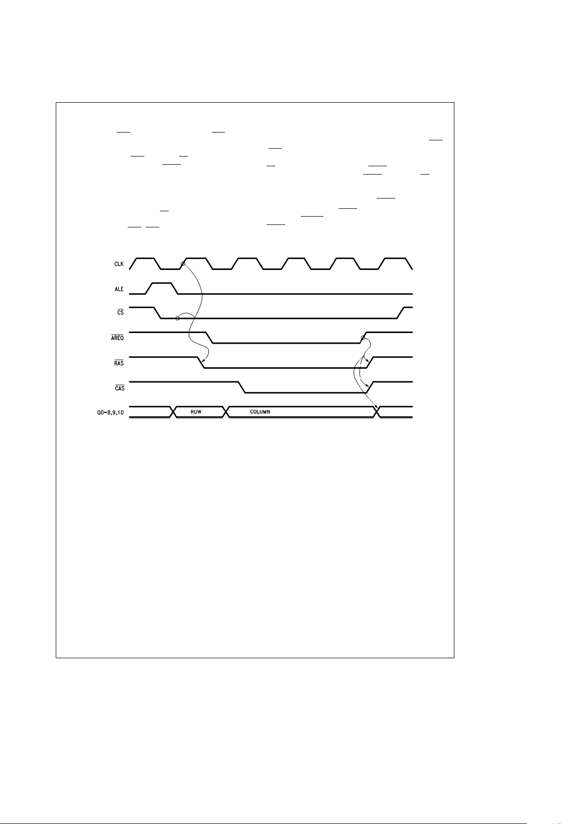
4.1 ACCESS MODE 0
Mode 0, synchronous access, is selected by negating the
input B1 during programming (B1
e
0). To initiate a Mode 0
access, ALE is pulse high and CS
is asserted. If precharge
time was met, a refresh of DRAM or a Port B access was
not in progress, the RAS
(RASs) would be asserted on the
first rising edge of clock. If a refresh or a Port B access is in
progress or precharge time is required, the controller will
wait until these events have taken place and assert RAS
(RASs) on the next positive edge of clock.
Sometime after the first positive edge of clock after ALE and
CS
have been asserted, the input AREQ must be asserted.
In single port applications, once AREQ
is asserted, CS can
be negated. On the other hand, ALE can stay asserted several periods of clock; however, ALE must be negated before
or during the period of CLK in which AREQ
is negated.
The controller samples AREQ on the every rising edge of
clock after DTACK
is asserted. The access will end when
AREQ
is sampled negated.
TL/F/11118– 8
FIGURE 8a. Access Mode 0
12
4.0 Port A Access Modes (Continued)
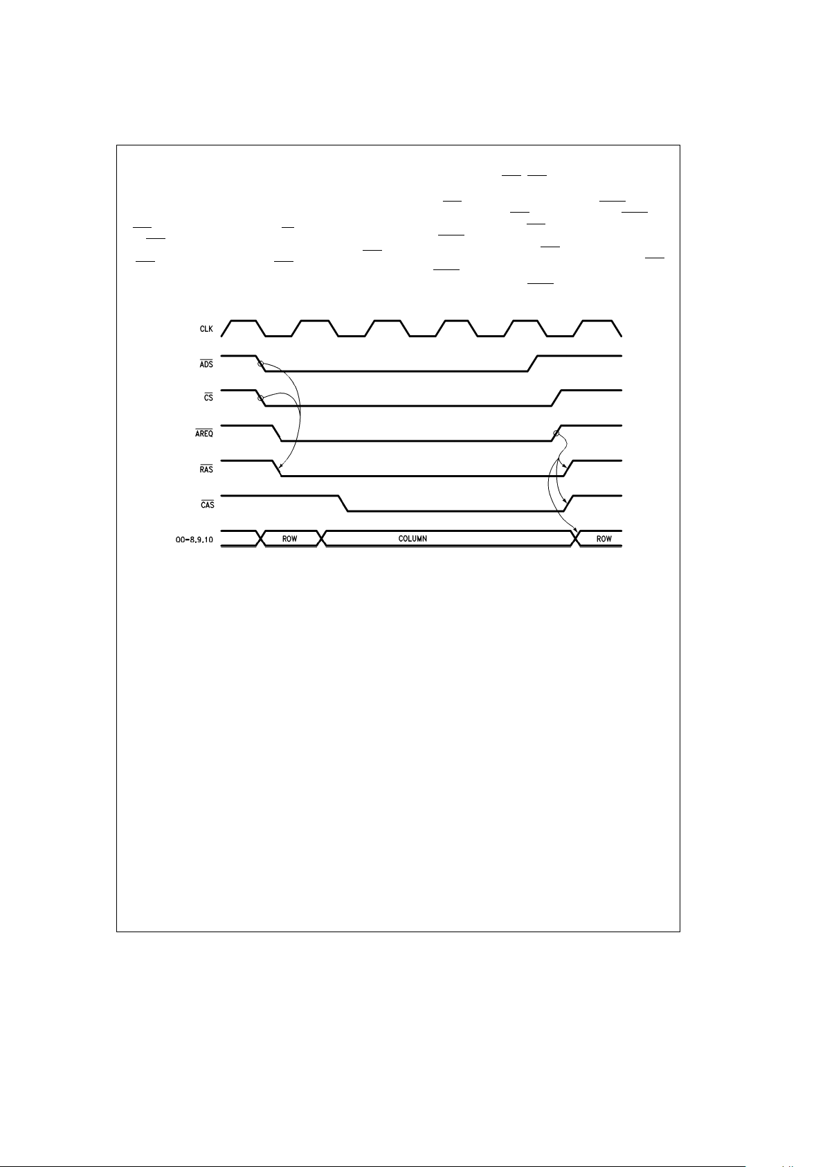
4.2 ACCESS MODE 1
Mode 1, asynchronous access, is selected by asserting the
input B1 during programming (B1
e
1). This mode allows accesses to start immediately from the access request input,
ADS
. To initiate a Mode 1 access, CS is asserted followed
by ADS
asserted. If precharge time was met, a refresh of
the DRAM or a Port B access was not in progress, the RAS
(RASs) would be asserted from ADS being asserted. If a
refresh or Port B access is in progress or precharge time is
required, the controller will wait until these events have tak-
en place and assert RAS
(RASs) from the next rising edge
of clock.
When ADS
is asserted or sometime after, AREQ must be
asserted. At this time, ADS
can be negated and AREQ will
continue the access. Also, ADS
can continue to be asserted
after AREQ
has been asserted and negated; however, a
new access will not start until ADS
is negated and asserted
again. When address pipelining is not implemented, ADS
and AREQ can be tied together.
The access will end when AREQ is negated.
TL/F/11118– 9
FIGURE 8b. Access Mode 1
13
4.0 Port A Access Modes (Continued)
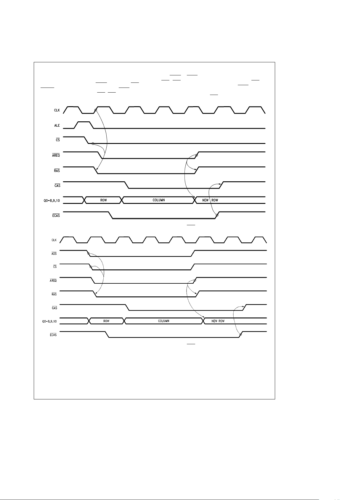
4.3 EXTENDING CAS WITH EITHER ACCESS MODE
In both access modes, once AREQ
is negated, RAS and
DTACK
if programmed will be negated. If ECAS0 was as-
serted (0) during programming, CAS
(CASs) will be negated
with AREQ
. If ECAS0 was negated (1) during programming,
CAS
(CASs) will continue to be asserted after RAS has
been negated, given that the appropriate ECAS
inputs are
asserted. This allows a DRAM to have data present on the
data out bus while gaining RAS
precharge time.
TL/F/11118– 10
FIGURE 9a. Access Mode 0 Extending CAS
TL/F/11118– 11
FIGURE 9b. Access Mode 1 Extending CAS
14
4.0 Port A Access Modes (Continued)
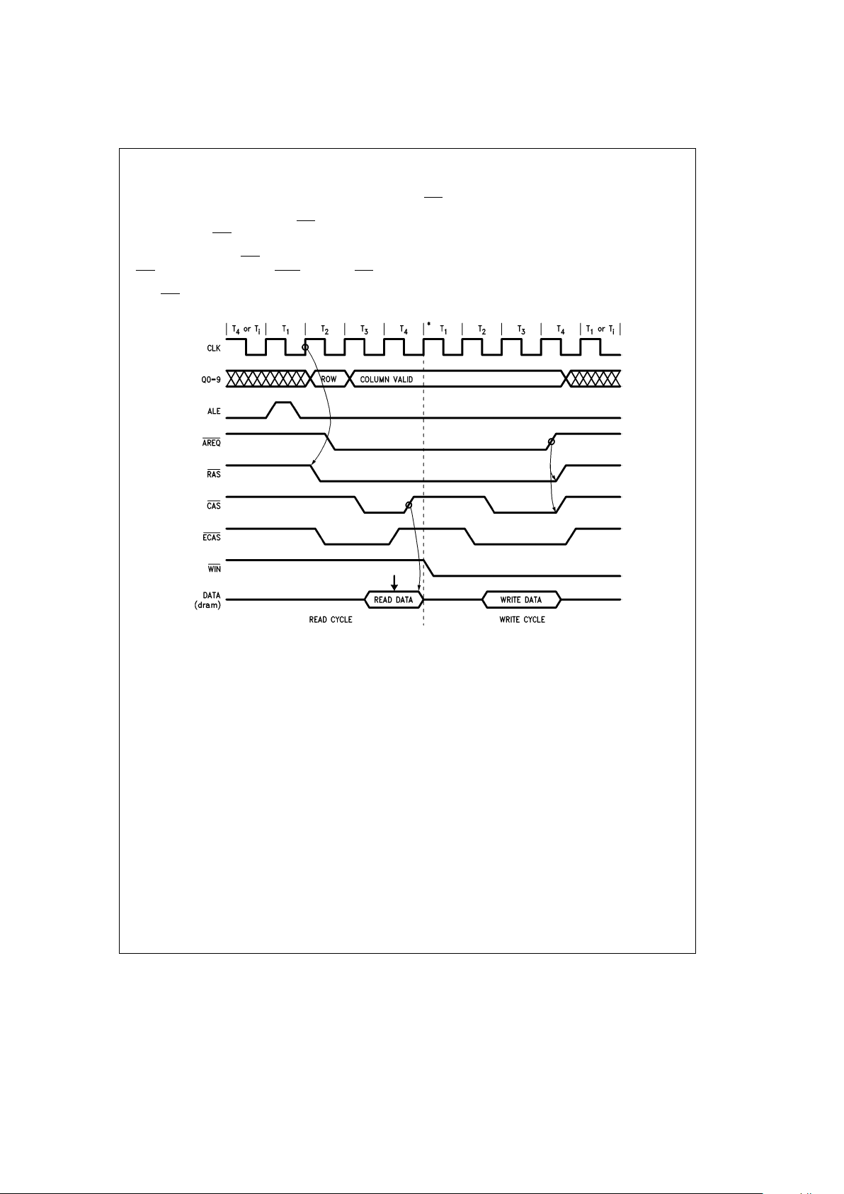
4.4 READ-MODIFY-WRITE CYCLES WITH EITHER ACCESS MODE
There are 2 methods by which this chip can be used to do
read-modify-write access cycles. The first method involves
doing a late write access where the WIN
input is asserted
some delay after CAS
is asserted. The second method involves doing a page mode read access followed by a page
mode write access with RAS
held low (see
Figure 9c
).
CASn must be toggled using the ECASn inputs and WIN has
to be changed from negated to asserted (read to write)
while CAS
is negated. This method is better than changing
WIN
from negated to asserted in a late write access because here a problem may arise with DATA IN and DATA
OUT being valid at the same time. This may result in a data
line trying to drive two different levels simultaneously. The
page mode method of a read-modify-write access allows
the user to have transceivers in the system because the
data in (read data) is guaranteed to be high impedance during the time the data out (write data) is valid.
TL/F/11118– 12
*There may be idle states inserted here by the CPU.
FIGURE 9c. Read-Modify-Write Access Cycle
15
4.0 Port A Access Modes (Continued)
4.5 ADDITIONAL ACCESS SUPPORT FEATURES
To support the different modes of accessing, the DP8430V/
31V/32V offer other access features. These additional features include: Address Latches and Column Increment (for
page/burst mode support), Address Pipelining, and Delay
CAS
(to allow the user with a multiplexed bus to ensure
valid data is present before CAS
is asserted).
4.5.1 Address Latches and Column Increment
The Address Latches can be programmed, through programming bit B0. They can be programmed to either latch
the address or remain in a fall-through mode. If the address
latches are used to latch the address, the controller will
function as follows:
In Mode 0, the rising edge of ALE places the latches in fallthrough, once ALE is negated, the address present in the
row, column and bank input is latched.
In Mode 1, the address latches are in fall through mode until
ADS
is asserted. ADS asserted latches the address.
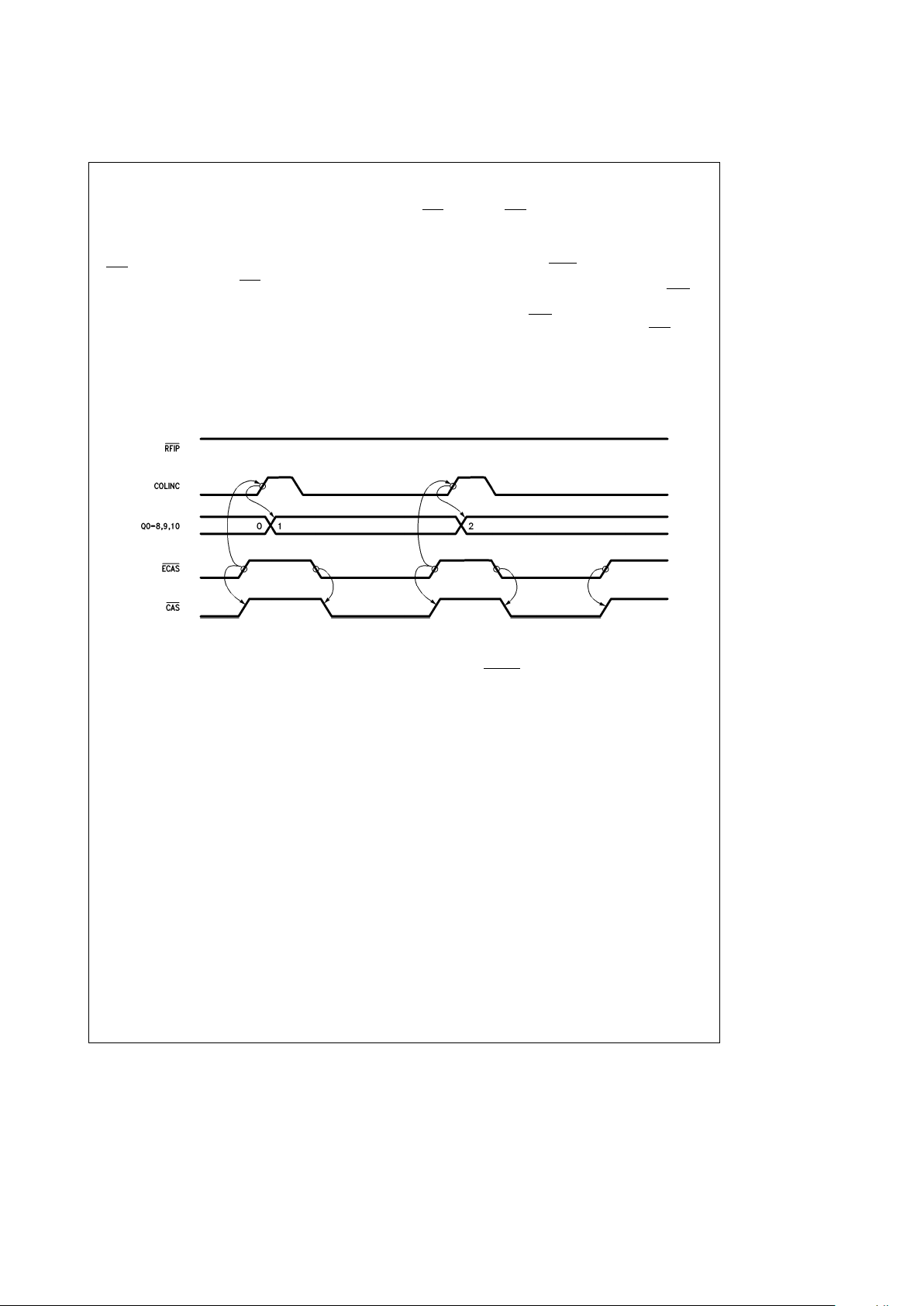
Once the address is latched, the column address can be
incremented with the input COLINC. COLINC can be used
for sequential accesses of static column DRAMs. COLINC
can also be used with the ECAS
inputs to support sequen-
tial accesses to page mode DRAMs as shown in
Figure 10
.
COLINC should only be asserted when the signal RFIP
is
negated during an access since this input functions as extended refresh when RFIP
is asserted. COLINC must be
negated (0) when the address is being latched (ADS
falling
edge in Mode 1). If COLINC is asserted with all of the bits of
the column address asserted (ones), the column address
will return to zero.
TL/F/11118– 13
FIGURE 10. Column Increment
The address latches function differently with the DP8432V.
The DP8432V will latch the address of the currently granted
port. If Port A is currently granted, the address will be
latched as described in Section 4.5.1. If Port A is not granted, and requests an access, the address will be latched on
the first or second positive edge of CLK after GRANTB has
been negated depending on the programming bits R0, R1.
For Port B, if GRANTB is asserted, the address will be
latched with AREQB
asserted. If GRANTB is negated, the
address will latch on the first or second positive edge of
CLK after GRANTB is asserted depending on the programming bits R0, R1.
16
4.0 Port A Access Modes (Continued)
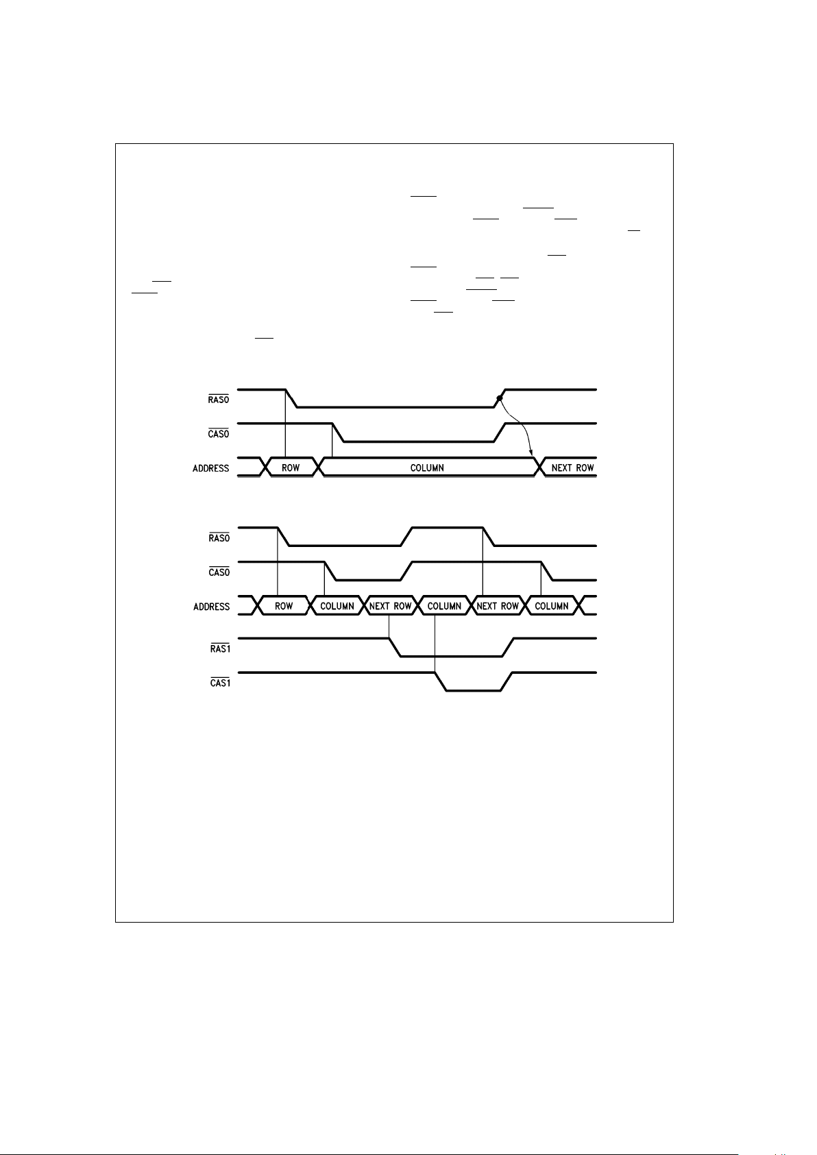
4.5.2 Address Pipelining
Address pipelining is the overlapping of accesses to different banks of DRAM. If the majority of successive accesses
are to a different bank, the accesses can be overlapped.
Because of this overlapping, the cycle time of the DRAM
accesses are greatly reduced. The DP8430V/31V/32V can
be programmed to allow a new row address to be placed on
the DRAM address bus after the column address hold time
has been met. At this time, a new access can be initiated
with ADS
or ALE, depending on the access mode, while
AREQ
is used to sustain the current access. The DP8432V
supports address pipelining for Port A only. This mode cannot be used with page, static column or nibble modes of
operations because the DRAM column address is switched
back to the row address after CAS
is asserted. This mode is
programmed through address bit R8 (see
Figures 11a
and
11b
).
During address pipelining in Mode 0, shown in
Figure 11c
,
ALE cannot be pulsed high to start another access until
AREQ
has been asserted for the previous access for at
least one period of CLK. DTACK
, if programmed, will be
negated once AREQ
is negated. WAIT, if programmed to
insert wait states, will be asserted once ALE and CS
are
asserted.
In Mode 1, shown in
Figure 11d
, ADS can be negated once
AREQ
is asserted. After meeting the minimum negated
pulse width for ADS
, ADS can again be asserted to start a
new access. DTACK
, if programmed, will be negated once
AREQ
is negated. WAIT, if programmed, will be asserted
once ADS
is asserted.
In either mode with either type of wait programmed, the
DP8430V/31V/32V will still delay the access for precharge
if sequential accesses are to the same bank or if a refresh
takes place.
TL/F/11118– 14
FIGURE 11a. Non-Address Pipelined Mode
TL/F/11118– 15
FIGURE 11b. Address Pipelined Mode
17
 Loading...