NSC DAC14135MT, DAC14135MTX Datasheet

N
DAC14135
14-bit, 135MSPS D/A Converter
November 1999
DAC14135
14-bit, 135MSPS D/A Converter
General Description
The DAC14135 is a monolithic 14-bit, 135MSPS digital-to-analog
converter. The device has been optimized for use in cellular base
stations and other applications where high resolution, high
sampling rate, wide dynamic range, and compact size are
required. The DAC14135 has many integrated features including
a proprietary segmented DAC core, differential current outputs, a
band-gap voltage reference, and TTL/CMOS compatible inputs.
The converter features an 85dBc spurious free dynamic range
(SFDR) at low frequencies and a 70dBc SFDR with 20MHz
output signals. The 48-pin TSSOP package provides an extremely
small footprint for applications where space is a critical consideration. The DAC14135 operates from a single +5V power supply.
The digital power supply can also operate from +3.3V for lower
power consumption and compatibility with +3.3V data inputs. The
DAC14135 is fabricated in a 0.5µm CMOS process and is specified over the industrial temperature range of -40°C to +85°C.
National Semiconductor thoroughly tests each part to verify full
compliance with the guaranteed specifications.
Features
• 135 MSPS
• Wide dynamic range
SFDR @ 1MHz f
SFDR @ 5MHz f
SFDR @ 20MHz f
: 85dBc
out
: 79dBc
out
out
: 70dBc
• Differential Current Outputs
• Low power consumption: 185mW
• Very small package: 48-pin TSSOP
• TTL/CMOS (+3.3V or +5V) inputs
Applications
• Cellular Basestations:
GSM, WCDMA, DAMPS, etc.
• Multi-carrier Basestations
• Multi-standard Basestations
• Direct digital synthesis (DDS)
• ADSL modems
• HFC modems
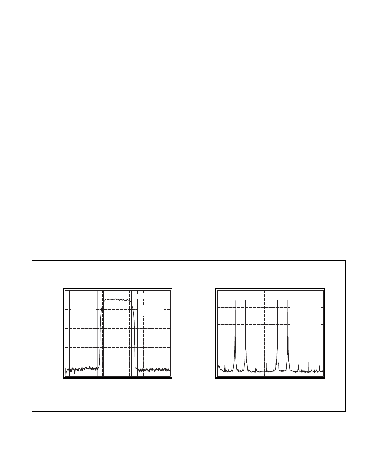
W-CDMA ACPR
-30
-40
-50
-60
-70
-80
Power (dB)
-90
-100
-110
-120
ACPR Lower
246810121416
72.1dB
Frequency (MHz)
Fs = 32.768MSPS
ACPR Upper
73dB
Four-Tone SFDR
0
SFDR > 70dBc
-20
-40
-60
Power (dB)
-80
-100
Fs = 135MSPS
F
= 6.2MHz
out1
F
= 9.31MHz
out2
= 18.8MHz
F
out3
F
= 21.95MHz
out4
Ampl. = 0dBFS
51015202530
Frequency (MHz)
© 1999 National Semiconductor Corporation http://www.national.com
Printed in the U.S.A.

µ
µ
DAC14135
Electrical Characteristics
(sample rate = 135MSPS, T
full scale current = 20mA,
= -40°C, T
min
differential 50 Ω doubly terminated output, unless specified otherwise)
= +85°C, AV
max
= +5V, DV
DD
= +5V, CV
DD
= +5V,
DD
PARAMETERS CONDITIONS TEMP RATINGS UNITS NOTES
MIN TYP MAX
RESOLUTION
FULL SCALE CURRENT
MAXIMUM CONVERSION RATE
SFDR (1
SFDR (1
SFDR (1
ST
Nyquist band)
ST
Nyquist band)
ST
Nyquist band)
NOISE FLOOR
DYNAMIC LINEARITY @ DV
= +5V sample rate = 135MSPS
DD
spurious-free dynamic range 1
= 1MHz 0dBFS Full 75 85 dBc 2
f
out
f
= 5MHz 0dBFS Full 70 79 dBc 2
out
f
= 20MHz 0dBFS Full 64 70 dBc 1 , 2
out
SFDR within a band f
f
= 1MHz, 0dBFS Full 75 85 dBc 2
out
f
= 5MHz, 0dBFS Full 70 79 dBc 2
out
f
= 20MHz, 0dBFS Full 64 70 dBc 1 , 2
out
f
= 5MHz, 0dBFS +25°C -146 dBFS/Hz
out
ST
Nyquist band
= 20MHz, 4MHz band +25°C 90 dBc
out
Full 14 Bits 1
Full 20 mA
Full 135 150 MSPS 1 , 2
four-tone SFDR 6.2, 9.31, 18.8, 21.95 MHz +25°C 72 dBc
DYNAMIC LINEARITY @ DV
spurious-free dynamic range 1
= 1MHz 0dBFS, DV
f
out
f
= 5MHz 0dBFS, DV
out
f
= 20MHz 0dBFS, DV
out
= +3.3V sample rate = 100MSPS
DD
ST
Nyquist band
= +3.3V +25°C 83 dBc
DD
= +3.3V +25°C 77 dBc
DD
= +3.3V +25°C 70 dBc
DD
DYNAMIC CHARACTERISTICS
glitch impulse +25°C 1 pV-s 3
settling time to 0.1% step size = I
/2 +25°C 30 ns
fullscale
rise time +25°C 0.4 ns
fall time +25°C 0.4 ns
DC ACCURACY AND PERFORMANCE
differential non-linearity +25°C ±1.0 LSB
integral non-linearity +25°C ±1.5 LSB
gain error +25°C ±5.0 % of FS
gain drift 20mA output current Full ±75 ppm/°C
offset error +25°C 10 nA
reference voltage +25°C 1.111 1.235 1.358 V
ANALOG OUTPUT PERFORMANCE
full scale current +25°C 20 mA
compliance voltage (high) +25°C 1.25 V
compliance voltage (low) +25°C -0.5 V
output resistance at mid-scale +25°C 150 k Ω
output capacitance at mid-scale +25°C 8.5 pF
DATA INPUTS
input logic low voltage, V
input logic high voltage, V
input logic low voltage, V
input logic high voltage, V
input logic low current, I
input logic high current, I
IL
IH
IL
IH
IL
IH
DV
= +3.3V Full 0.9 V 1
DD
DV
= +3.3V Full 2.4 V 1
DD
Full 1.3 V 1
Full 3.5 V 1
Full -10 10
Full -10 10
A1
A1
TIMING
maximum conversion rate Full 135 150 MSPS 1, 2
setup time (T
hold time (T
propagation delay (T
latency +25°C 1
) +25°C 0.5 ns
S
) +25°C 4.5 ns
H
) +25°C 2 ns
PD
clk cycles
CLOCK INPUTS
clock inputs internal self bias +25°C 1.5 V
differential clock input swing Full 1.5 Vpp
differential clock input slew rate Full 1 V/ns
clock input impedance (single-ended) +25°C 1.2 k Ω
Min/max ratings are based on product characterization and simulation. Individual parameters are tested as noted. Outgoing quality levels are
determined from tested parameters.
http://www.national.com
2

DAC14135
Electrical Characteristics
(sample rate = 135MSPS, T
full scale current = 20mA,
= -40°C, T
min
differential 50 Ω doubly terminated output, unless specified otherwise)
= +85°C, AV
max
= +5V, DV
DD
= +5V, CV
DD
= +5V,
DD
PARAMETERS CONDITIONS TEMP RATINGS UNITS NOTES
MIN TYP MAX
POWER REQUIREMENTS
analog supply current +25°C 28 35 mA 1
digital supply current 135MSPS, DV
digital supply current 100MSPS, DV
power consumption 135MSPS, DV
power consumption 100MSPS, DV
AV
power supply rejection ratio at mid-scale +25°C 1.0 %FS/V
DD
Min/max ratings are based on product characterization and simulation. Individual parameters are tested as noted. Outgoing quality levels are
determined from tested parameters.
1) These parameters are 100% tested at 25°C.
2) These parameters are sample tested at -40°C, +25°C and +85°C.
Absolute Maximum Ratings
positive supply voltage (V
analog output voltage range -0.7V to +V
digital input voltage range -0.5V to +V
output short circuit duration infinite
junction temperature 175°C
storage temperature range -65°C to 150°C
lead solder duration (+300°C) 10sec
Note: Absolute maximum ratings are limiting values , to be applied individually, and
beyond which the serviceability of the circuit may be impaired. Functional
operability under any of these conditions is not necessarily implied. Exposure to
maximum ratings for extended periods may affect device reliability.
) -0.5V to +6V
DD
= +5V +25°C 9 15 mA 1
DD
= +3.3V +25°C 4.5 mA
DD
= +5V +25°C 185 mW
DD
= +3.3V +25°C 150 mW
DD
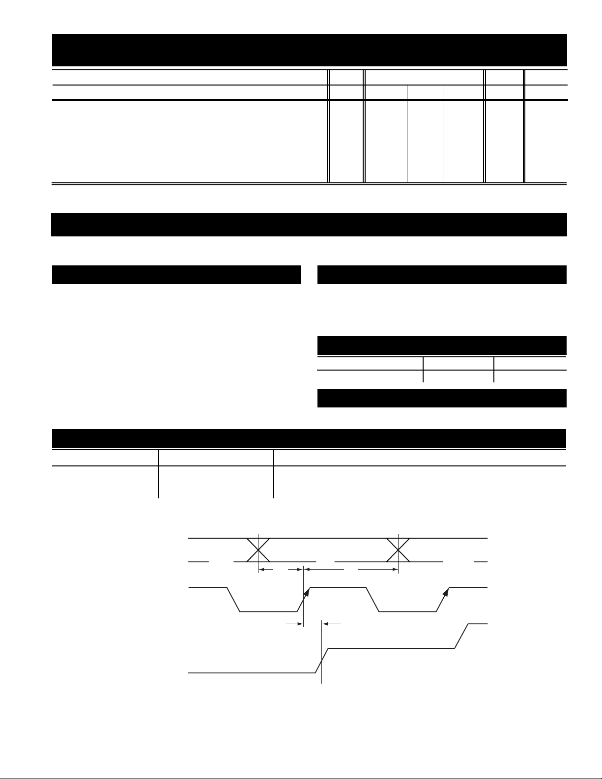
CLC5958 Timing Diagram
Notes
3) Defined as the net area of undesired output transients in pV-s
at a major transition.
Recommended Operating Conditions
positive analog supply voltage +5V ±5%
positive digital supply voltage +3.3V or +5V ±5%
DD
positive clock supply voltage +5V ±5%
DD
operating temperature range -40°C to +85°C
Pac kage Thermal Resistance
Package
48-pin TSSOP 56°C/W 16°C/W
θ
JA
Pac kage Transistor Count
Transistor count 8,600
θ
JC
Ordering Information
Model Temperature Range Description
DAC14135MT -40°C to +85°C 48-pin TSSOP (industrial temperature range)
DAC14135MTX -40°C to +85°C 48-pin TSSOP (TNR 1000 pc reel)
DAC14135PCASM Fully loaded evaluation board with DAC14135 … ready for test.
D0 – D13
CLOCK T
IoutT or
IoutF
N-1
N N+1
T
S
T
H
T
PD
N-2
DA C14135 Timing Diagram
N
N-1
NOTE: 1 clock cycle latency
3
http://www.national.com

DAC14135 Pin Definitions
(MSB)
(LSB)
1DGND 48 DGND
2DGND 47 DGND
3DGND 46 DGND
4DV
DD
5DV
DD
6 D13 43 CV
7D12 42 Clock T
DAC14135
8D11 41 Clock F
9D10 40 CGND
10D9 39 NC
11D8 38 AGND
12D7 37 I
13D6 36 I
14D5 35 AGND
15D4 34 AV
16D3 33 AV
17D2 32 AGND
18D1 31 REFCOMP
19D0 30 FSADJ
20DS 29 REFIO
21NC 28 REFLO
22AGND 27 AGND
23AGND 26 AGND
24AGND 25 AGND
45 DV
44 DV
OUTT
OUTF
DD
DD
DD
DD
DD
I
OUTT
I
OUTF
Clock T
(Pins 37, 36) Differential current outputs. Output compliance
range is -0.5V to +1.25V.
(Pins 42, 41) Differential clock inputs. Bypass CLOCKF with
Clock F a 0.1 µ F capacitor to CGND if using single-ended clock on
CLOCKT. Both inputs have internal self-bias at
approximately 1.5V.
D0 - D13 (Pins 6 - 19) Digital data inputs. CMOS (+3.3V and +5V) and
TTL (with +3.3V DVDD) compatible. D13 is the MSB.
DS (Pin 20) Data scramble input. If not used, either connect to
ground or leave unconnected.
AGND (Pins 22 - 27, 32, 35, 38) Analog ground.
DGND (Pins 1 - 3, 46 - 48) Digital ground.
CGND (Pin 40) Clock ground. Connect to AGND.
AV
DD
(Pins 33, 34) +5V power supply for the analog section.
Bypass to analog ground with a 0.1µF capacitor.
DV
DD
(Pins 4, 5, 44, 45) +5V or +3.3V power supply for the digital
section. Bypass to digital ground with a 0.1µF capacitor.
CV
DD
(Pin 43) Internal clock buffer power supply. Bypass to clock
ground with 0.1µF capacitor.
REFIO (Pin 29) Internal voltage reference output (Vref) or voltage
reference input. Nominally +1.235V. Can be overdriven with
an external reference. Bypass to A GND with 0.1µF capacitor.
REFLO (Pin 28) Ground for reference circuitry. Should be connected
to AGND.
FSADJ (Pin 30) Full scale current adjust. Must be connected with an
external resistor (Rset) or an external current source (Iref) to
analog ground.
Ifullscale (mA) = 42.67 x Iref = 42.67 x REFIO/Rset
REFCOMP (Pin 31) Compensation pin for the internal reference
circuitry. Bypass to analog ground with a 0.1µF capacitor.
NC (Pins 21, 39) No connect.
http://www.national.com
4
 Loading...