

TL/H/5587
ADC0811 8-Bit Serial I/O A/D Converter With 11-Channel Multiplexer
December 1994
ADC0811 8-Bit Serial I/O A/D Converter
With 11-Channel Multiplexer
General Description
The ADC0811 is an 8-Bit successive approximation A/D
converter with simultaneous serial I/O. The serial input controls an analog multiplexer which selects from 11 input
channels or an internal half scale test voltage.
An input sample-and-hold is implemented by a capacitive
reference ladder and sampled data comparator. This allows
the input signal to vary during the conversion cycle.
Separate serial I/O and conversion clock inputs are provided to facilitate the interface to various microprocessors.
Features
Y
Separate asynchronous converter clock and serial data
I/O clock.
Y
11-Channel multiplexer with 4-Bit serial address logic.
Y
Built-in sample and hold function.
Y
Ratiometric or absolute voltage referencing.
Y
No zero or full-scale adjust required.
Y
Internally addressable test voltage.
Y
0V to 5V input range with single 5V power supply.
Y
TTL/MOS input/output compatible.
Y
0.3×standard width 20-pin dip or 20-pin molded chip
carrier
Key Specifications
Y
Resolution 8-Bits
Y
Total unadjusted error
g
(/2LSB andg1LSB
Y
Single supply 5V
DC
Y
Low Power 15 mW
Y
Conversion Time 32 mS
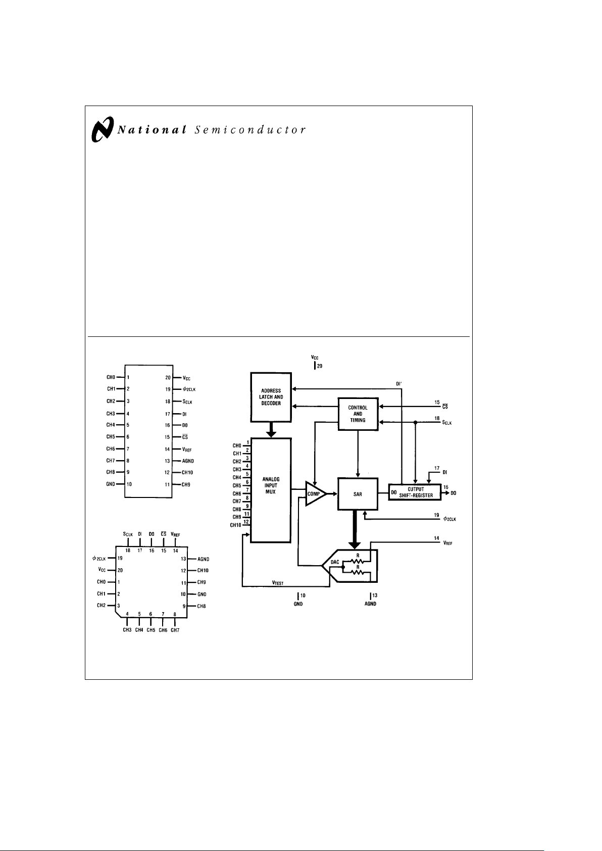
Connection Diagrams
Dual-In-Line Package
TL/H/5587– 1
Top View
Molded Chip Carrier (PCC) Package
TL/H/5587– 2
Top View
Order Number ADC0811J,N,V
See NS Packages J20A, N20A, V20A
Use Ordering Information
Functional Diagram
TL/H/5587– 3
C
1995 National Semiconductor Corporation RRD-B30M115/Printed in U. S. A.
Absolute Maximum Ratings (Notes1&2)
If Military/Aerospace specified devices are required,
please contact the National Semiconductor Sales
Office/Distributors for availability and specifications.
Supply Voltage (V
CC
) 6.5V
Voltage
Inputs and Outputs
b
0.3V to V
CC
a
0.3V
Input Current Per Pin (Note 3)
g
5mA
Total Package Input Current (Note 3)
g
20mA
Storage Temperature
b
65§Ctoa150§C
Package Dissipation at T
A
e
25§C 875 mW
Lead Temp. (Soldering, 10 seconds)
Dual-In-Line Package (plastic) 260
§
C
Dual-In-Line Package (ceramic) 300
§
C
Molded Chip Carrier Package
Vapor Phase (60 seconds) 215
§
C
Infrared (15 seconds) 220
§
C
ESD Susceptibility (Note 11) 2000V
Operating Ratings (Notes1&2)
Supply Voltage (V
CC
) 4.5 VDCto 6.0 V
DC
Temperature Range T
MIN
s
T
A
s
T
MAX
ADC0811BCN, ADC0811CCN 0§CsT
A
s
70§C
ADC0811BCV
b
40§CsT
A
s
85§C
ADC0811CCJ, ADC0811CCV
b
40§CsT
A
s
85§C
Electrical Characteristics
The following specifications apply for V
CC
e
4.75V to 5.25V, V
REF
ea
4.6V to (V
CC
a
0.1V), w
2 CLK
e
2.097 MHz unless
otherwise specified. Boldface limits apply from T
MIN
to T
MAX
; all other limits T
A
e
T
J
e
25§C.
Parameter Conditions
ADC0811CCJ
ADC0811BCN, ADC0811BCV
Units
ADC0811CCN, ADC0811CCV
Typical
Tested Design
Typical
Tested Design
(Note 6)
Limit Limit
(Note 6)
Limit Limit
(Note 7) (Note 8) (Note 7) (Note 8)
CONVERTER AND MULTIPLEXER CHARACTERISTICS
Maximum Total V
REF
e
5.00 V
DC
Unadjusted Error (Note 4)
ADC0811BCN, ADC0811BCV
g
(/2
g
(/2 LSB
ADC0811CCN, ADC0811CCV
g
1
g
1 LSB
ADC0811CCJ
g
1 LSB
Minimum Reference
8 5 8 5 kX
Input Resistance
Maximum Reference
8 11 811 11 kX
Input Resistance
Maximum Analog Input Range (Note 5) V
CC
a
0.05 V
CC
a
0.05 V
CC
a
0.05 V
Minimum Analog Input Range GNDb0.05 GNDb0.05 GNDb0.05 V
On Channel Leakage Current
ADC0811BCJ, CCJ, BCN, CCN, On Channel
e
5V 1000 400 1000 nA
BCV, CCV Off Channel
e
0V
ADC0811CJ, BJ 1000 nA
ADC0811BCJ, CCJ, BCN, CCN, On Channele0V
b
1000
b
400
b
1000 nA
BCV, CCV Off Channel
e
5V
ADC0811BJ, CJ (Note 9)
b
1000 nA
Off Channel Leakage Current
ADC0811BCJ, CCJ, BCN, CCN, On Channel
e
5V
b
1000
b
400 1000 nA
BCV, CCV Off Channel
e
0V
ADC0811CJ, BJ
b
1000 nA
ADC0811BCJ, CCJ, BCN, CCN, On Channele0V 1000 400 1000 nA
BCV, CCV Off Channel
e
5V
ADC0811BJ, CJ (Note 9) 1000 nA
Minimum V
TEST
V
REF
e
VCC, (Note 10)
Internal Test Voltage CH 11 Selected 125 125 125 Counts
Maximum V
TEST
V
REF
e
VCC, (Note 10)
Internal Test Voltage CH 11 Selected 130 130 130 Counts
2
Electrical Characteristics
The following specifications apply for V
CC
e
4.75V to 5.25V, V
REF
ea
4.6V to (V
CC
a
0.1V), w
2 CLK
e
2.097 MHz unless
otherwise specified. Boldface limits apply from T
MIN
to T
MAX
; all other limits T
A
e
T
J
e
25§C. (Continued)
Parameter Conditions
ADC0811CCJ
ADC0811BCN, ADC0811BCV
Units
ADC0811CCN, ADC0811CCV
Typical
Tested Design
Typical
Tested Design
(Note 6)
Limit Limit
(Note 6)
Limit Limit
(Note 7) (Note 8) (Note 7) (Note 8)
DIGITAL AND DC CHARACTERISTICS
V
IN(1)
, Logical ‘‘1’’ Input V
CC
e
5.25V 2.0 2.0 2.0 V
Voltage (Min)
V
IN(0)
, Logical ‘‘0’’ Input V
CC
e
4.75V 0.8 0.8 0.8 V
Voltage (Max)
I
IN(1)
, Logical ‘‘1’’ Input V
IN
e
5.0V 0.005 2.5 0.005 2.5 2.5 mA
Current (Max)
I
IN(0)
, Logical ‘‘0’’ Input V
IN
e
0V
b
0.005
b
2.5
b
0.005 2.5
b
2.5 mA
Current (Max)
V
OUT(1)
, Logical ‘‘1’’ V
CC
e
4.75V
Output Voltage (Min) I
OUT
eb
360 mA 2.4 2.4 2.4 V
I
OUT
eb
10 mA 4.5 4.5 4.5 V
V
OUT(0)
, Logical ‘‘0’’ V
CC
e
5.25V 0.4 0.4 0.4 V
Output Voltage (Max) I
OUT
e
1.6 mA
I
OUT
, TRI-STATE Output V
OUT
e
0V
b
0.01
b
3
b
0.01
b
3
b
3 mA
Current (Max) V
OUT
e
5V 0.01 3 0.01 3 3 mA
I
SOURCE
, Output Source V
OUT
e
0V
b
12
b
6.5
b
14
b
6.5
b
6.5 mA
Current (Min)
I
SINK
, Output Sink Current (Min) V
OUT
e
V
CC
18 8.0 16 8.0 8.0 mA
ICC, Supply Current (Max) CSe1, V
REF
Open 1 2.5 1 2.5 2.5 mA
I
REF
(Max) V
REF
e
5V 0.7 1 0.7 1 1 mA
AC CHARACTERISTICS
Tested Design
Parameter Conditions Typical Limit Limit Units
(Note 6) (Note 7) (Note 8)
w
2 CLK
, w2Clock Frequency MIN 0.70 1.0
MHz
MAX 3.0 2.0 2.1
S
CLK
, Serial Data Clock MIN 5.0
KHz
Frequency
MAX 700 525 525
TC, Conversion Process Time MIN Not Including MUX 48 48 w2cycles
Addressing and
MAX
Analog Input
64 64
Sampling Times
t
ACC
, Access Time Delay From CS MIN 1 w2cycles
Falling Edge to DO Data Valid MAX 3
t
SET-UP
, Minimum Set-up Time of CS Falling
4/w
2CLK
a
1
2S
CLK
sec
Edge to S
CLK
Rising Edge
t
HCS
,CSHold Time After the Falling
0 ns
Edge of S
CLK
tCS, Total CS Low Time MIN t
set-up
a
8/S
CLK
sec
MAX tCS(min)a48/w
2CLK
sec
t
HDI
, Minimum DI Hold Time from
0 0 ns
S
CLK
Rising Edge
t
HDO
, Minimum DO Hold Time from S
CLK
R
L
e
30k,
10 ns
Falling Edge C
L
e
100 pF
3
Electrical Characteristics
The following specifications apply for V
CC
e
4.75V to 5.25V, V
REF
ea
4.6V to (V
CC
a
0.1V), w
2 CLK
e
2.097 MHz unless
otherwise specified. Boldface limits apply from T
MIN
to T
MAX
; all other limits T
A
e
T
J
e
25§C. (Continued)
Typical
Tested Design
Parameter Conditions
(Note 6)
Limit Limit Units
(Note 7) (Note 8)
AC CHARACTERISTICS (Continued)
t
SDI
, Minimum DI Set-up Time to S
CLK
200 400 ns
Rising Edge
t
DDO
, Maximum Delay From S
CLK
R
L
e
30k,
180 400 400 ns
Falling Edge to DO Data Valid C
L
e
100 pF
t
TRI
, Maximum DO Hold Time, R
L
e
3k,
(CS
Rising edge to DO C
L
e
100 pF 90 150 150 ns
TRI-STATE)
tCA, Analog After Address Is Latched
4/S
CLK
a
1 ms sec
Sampling Time CS
e
Low
t
RDO
, Maximum DO R
L
e
30 kX, ‘‘TRI-STATE’’ to ‘‘HIGH’’ State 75 150 150
ns
Rise Time C
L
e
100 pf ‘‘LOW’’ to ‘‘HIGH’’ State 150 300 300
t
FDO
, Maximum DO R
L
e
30 kX, ‘‘TRI-STATE’’ to ‘‘LOW’’ State 75 150 150
ns
Fall Time C
L
e
100 pf ‘‘HIGH’’ to ‘‘LOW’’ State 150 300 300
CIN, Maximum Input Analog Inputs, ANO– AN10 and V
REF
11 55
pF
Capacitance All Others 5 15
Note 1: Absolute Maximum Ratings indicate limits beyond which damage to the device may occur. DC and AC electrical specifications do not apply when operating
the device beyond its specified operating conditions.
Note 2: All voltages are measured with respect to ground.
Note 3: Under over voltage conditions (V
IN
k
0V and V
IN
l
VCC) the maximum input current at any one pin isg5 mA. If the voltage at more than one pin exceeds
V
CC
a
.3V the total package current must be limited to 20 mA. For example the maximum number of pins that can be over driven at the maximum current level of
g
5 mA is four.
Note 4: Total unadjusted error includes offset, full-scale, linearity, multiplexer, and hold step errors.
Note 5: Two on-chip diodes are tied to each analog input, which will forward-conduct for analog input voltages one diode drop below ground or one diode drop
greater than V
CC
supply. Be careful during testing at low VCClevels (4.5V), as high level analog inputs (5V) can cause this input diode to conduct, especially at
elevated temperatures, and cause errors for analog inputs near full-scale. The spec allows 50 mV forward bias of either diode. This means that as long as the
analog V
IN
does not exceed the supply voltage by more than 50 mV, the output code will be correct. To achieve an absolute 0 VDCto5VDCinput voltage range will
therefore require a minimum supply voltage of 4.950 V
DC
over temperature variations, initial tolerance and loading.
Note 6: Typicals are at 25
§
C and represent most likely parametric norm.
Note 7: Guaranteed and 100% production tested under worst case condition.
Note 8: Guaranteed, but not 100% production tested. These limits are not used to calculate outgoing quality levels.
Note 9: Channel leakage current is measured after the channel selection.
Note 10: 1 count
e
V
REF
/256.
Note 11: Human body model, 100 pF discharged through a 1.5 kX resistor.
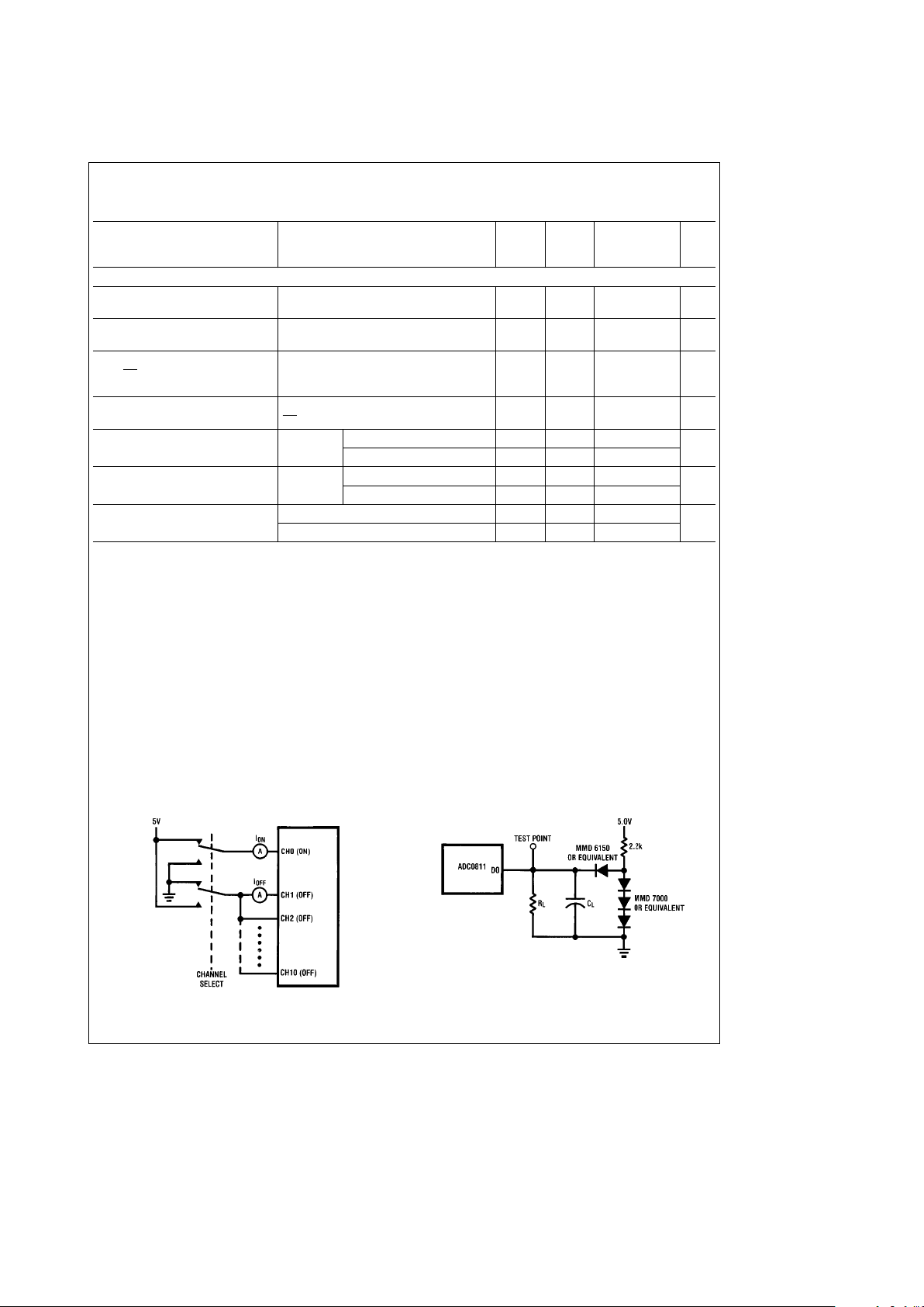
Test Circuits
Leakage Current
TL/H/5587– 17
D0 Except ‘‘TRI-STATE’’
TL/H/5587– 6
4
Test Circuits (Continued)
t
TRI
‘‘TRI-STATE’’
TL/H/5587– 22
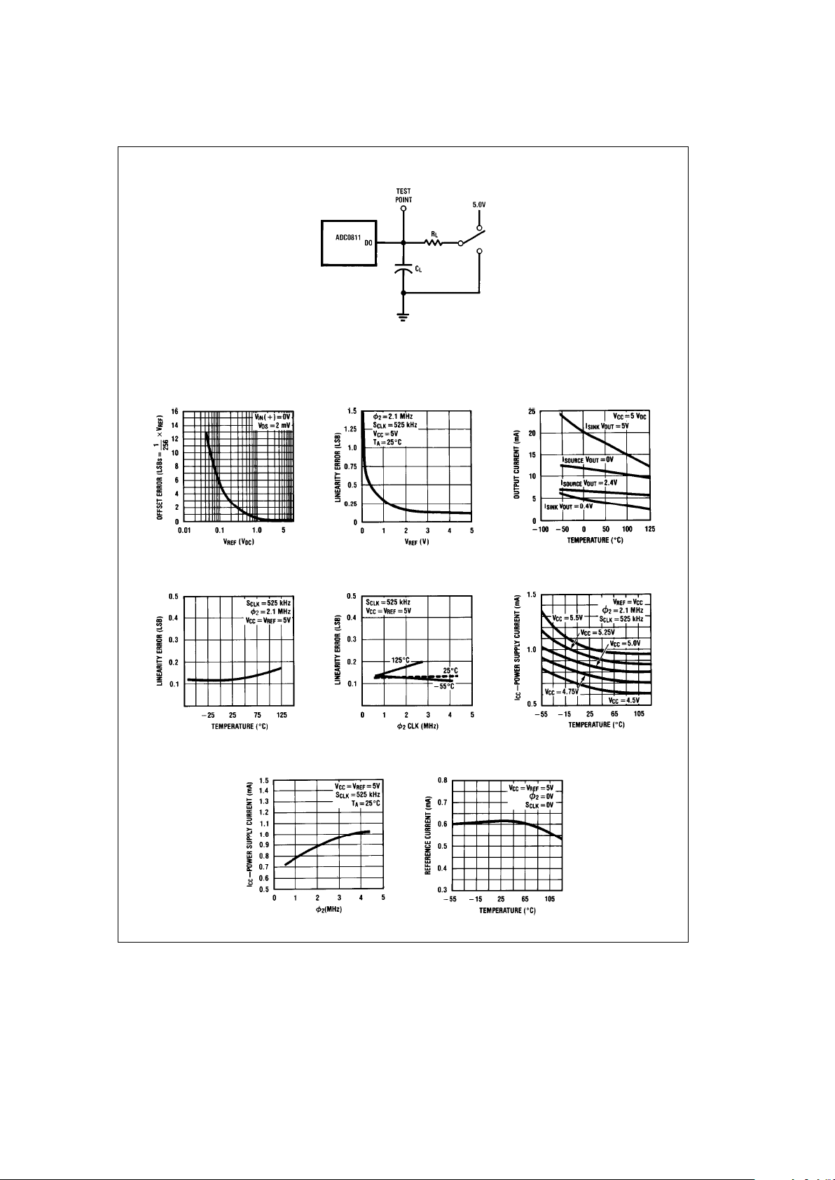
Typical Performance Characteristics
Unadjusted Offset Error vs
V
REF
Voltage
Linearity Error vs V
REF
Voltage
Output Current vs
Temperature
Linearity vs Temperature
Linearity vs w
2
Clock
Frequency
Power Supply Current
vs Temperature
Power Supply Current vs
w
2
Clock Frequency
Resistive Ladder Reference
Current vs Temperature
TL/H/5587– 16
5

Timing Diagrams
D0 ‘‘TRI-STATE’’ Rise & Fall Times
TL/H/5587– 13
D0 Low to High State
TL/H/5587– 14
D0 High to Low State
TL/H/5587– 15
Timing with a continuous S
CLK
TL/H/5587– 11
*Strobing CS High and Low will abort the present conversion and initiate a new serial I/O exchange.
Timing with a gated S
CLK
and CS Continuously Low
TL/H/5587– 9
Using CS To TRI-STATE D0
TL/H/5587– 10
Note: Strobing CS Low during this time interval will abort the conversion in process.
6

Timing Diagrams (Continued)
CS
High During Conversion
TL/H/5587– 4
CS Low During Conversion
TL/H/5587– 5
Note: DO and DI lines share the 8-bit I/O shift register(see Functional Block Diagram). Since the MUX address bits are shifted in on S
CLK
rising edges while S
CLK
falling edges shift out conversion data on DO, the eighth falling edge of S
CLK
will shift out the MSB MUX address bit (A7) on DO. Thus, if addressing channels
CH8– CH10, a high DO will occur momentarily (one w
2
clock period) until the 8-bit I/O shift register is cleared by the internal EOC signal.
Channel Addressing Table
TABLE I. ADC 0811 Channel Addressing
MUX ADDRESS ANALOG CHANNEL
A7A6A5A4A3A2A1A
0
SELECTED
00 00XXXX CH0
00 01XXXX CH1
00 10XXXX CH2
00 11XXXX CH3
01 00XXXX CH4
01 01XXXX CH5
01 10XXXX CH6
01 11XXXX CH7
10 00XXXX CH8
10 01XXXX CH9
10 10XXXX CH10
10 11XXXX V
TEST
11XXXXXXLOGIC TEST MODE*
* Analog channel inputs CH0 thru CH3 are logic outputs
7

Functional Block Diagram
TL/H/5587– 8
8

Functional Description
1.0 DIGITAL INTERFACE
The ADC0811 uses five input/output pins to implement the
serial interface. Taking chip select (CS
) low enables the I/O
data lines (DO and DI) and the serial clock input (S
CLK
). The
result of the last conversion is transmitted by the A/D on the
DO line, while simultaneously the DI line receives the address data that selects the mux channel for the next conversion. The mux address is shifted in on the rising edge of
S
CLK
and the conversion data is shifted out on the falling
edge. It takes eight S
CLK
cycles to complete the serial I/O.
A second clock (w
2
) controls the SAR during the conversion
process and must be continuously enabled.
1.1 CONTINUOUS S
CLK
With a continuous S
CLK
input CS must be used to synchro-
nize the serial data exchange (see
Figure 1
). The ADC0811
recognizes a valid CS
one to three w2clock periods after
the actual falling edge of CS
. This is implemented to ensure
noise immunity of the CS
signal. Any spikes on CS less than
one w
2
clock period will be ignored. CS must remain low
during the complete I/O exchange which takes eight S
CLK
cycles. Although CS is not immediately acknowledged for
the purpose of starting a new conversion, the falling edge of
CS
immediately enables DO to output the MSB (D7) of the
previous conversion.
The first S
CLK
rising edge will be acknowledged after a set-
up time (t
set-up
) has elapsed from the falling edge of CS.
This and the following seven S
CLK
rising edges will shift in
thechanneladdress for the analog multiplexer.Sincethere are
12 channels only four address bits are utilized. The first four
S
CLK
cycles clock in the mux address, during the next four
S
CLK
cycles the analog input is selected and sampled. During
this mux address/sample cycle, data from the last conversion is also clocked out on DO. Since D7 was clocked out
on the falling edge of CS
only data bits D6 – D0 remain to be
received. The following seven falling edges of S
CLK
shift out
this data on DO.
The 8th S
CLK
falling edge initiates the beginning of the A/D’s
actual conversion process which takes between 48 to 64 w
2
cycles (TC). During this time CS can go high to TRI-STATE
DO and disable the S
CLK
input or it can remain low. If CS is
held low a new I/O exchange will not start until the conversion sequence has been completed, however once the conversion ends serial I/O will immediately begin. Since there is
an ambiguity in the conversion time (T
C
) synchronizing the
data exchange is impossible. Therefore CS
should go high
before the 48th w
2
clock has elasped and return low after
the 64th w
2
to synchronize serial communication.
A conversion or I/O operation can be aborted at any time by
strobing CS
.IfCSis high or low less than one w2clock it will
be ignored by the A/D. If the CS
is strobed high or low
between 1 to 3 w
2
clocks the A/D may or may not respond.
Therefore CS
must be strobed high or low greater than 3 w
2
clocks to ensure recognition. If a conversion or I/O exchange is aborted while in process the consequent data
output will be erroneous until a complete conversion sequence has been implemented.
1.2 DISCONTINUOUS S
CLK
Another way to accomplish synchronous serial communication is to tie CS
low continuously and disable S
CLK
after its
8th falling edge (see
Figure 2
). S
CLK
must remain low for
TL/H/5587– 18
FIGURE 1
TL/H/5587– 19
FIGURE 2
9

Functional Description (Continued)
at least 64 w
2
clocks to insure that the A/D has completed
its conversion. If S
CLK
is enabled sooner, synchronizing to
the data output on DO is not possible since an end of conversion signal from the A/D is not available and the actual
conversion time is not known. With CS
low during the con-
version time (64 w
2
max) DO will go low after the eighth
falling edge of S
CLK
and remain low until the conversion is
completed. Once the conversion is through DO will transmit
the MSB. The rest of the data will be shifted out once S
CLK
is enabled as discussed previously.
If CS
goes high during the conversion sequence DO is tri-
stated, and the result is not affected so long as CS
remains
high until the end of the conversion.
1.2 MULTIPLEXER ADDRESSING
The four bit mux address is shifted, MSB first, into DI. Input
data corresponds to the channel selected as shown in table
1. Care should be taken not to send an address greater than
or equal to twelve (11XX) as this puts the A/D in a digital
testing mode. In this mode the analog inputs CH0 thru CH3
become digital outputs, for our use in production testing.
2.0 ANALOG INPUT
2.1 THE INPUT SAMPLE AND HOLD
The ADC0811’s sample/hold capacitor is implemented in its
capacitive ladder structure. After the channel address is received, the ladder is switched to sample the proper analog
input. This sampling mode is maintained for 1 msec after the
eighth S
CLK
falling edge. The hold mode is initiated with the
start of the conversion process. An acquisition window of
4t
S
CLK
a
1 msec is therefore available to allow the ladder
capacitance to settle to the analog input voltage. Any
change in the analog voltage before or after the acquisition
window will not effect the A/D conversion result.
In the most simple case, the ladder’s acquisition time is determined by the R
on
(3K) of the multiplexer switches and the
total ladder capacitance (90pf). These values yield an acquisition time of about 2 msec for a full scale reading. Therefore the analog input must be stable for at least 2 msec
before and 1 msec after the eighth S
CLK
falling edge to
ensure a proper conversion. External input source resistance and capacitance will lengthen the acquisition time and
should be accounted for.
Other conventional sample and hold error specifications are
included in the error and timing specs of the A/D. The hold
step and gain error sample/hold specs are taken into account in the ADC0811’s total unadjusted error, while the
hold settling time is included in the A/D’s max conversion
time of 64 w
2
clock periods. The hold droop rate can be
thought of as being zero since an unlimited amount of time
can pass between a conversion and the reading of data.
However, once the data is read it is lost and another conversion is started.
Typical Applications
ADC0811-INS8048 INTERFACE
TL/H/5587– 21
10

ADC0811 FUNCTIONAL CIRCUIT
TL/H/5587– 20
Ordering Information
Temperature Range 0§Cto70§C
b
40§Ctoa85§C
Total Unadjusted
g
(/2 LSB ADC0811BCN ADC0811BCV
Error
g
1 LSB ADC0811CCN ADC0811CCJ
ADC0811CCV
Package Outline N20A J20A, V20A
11

12

Physical Dimensions inches (millimeters)
Ceramic Dual-In-Line Package (J)
Order Number ADC0811CCJ
NS Package J20A
Molded Dual-In-Line Package (N)
Order Number ADC0811BCN, CCN
NS Package N20A
13

ADC0811 8-Bit Serial I/O A/D Converter With 11-Channel Multiplexer
Physical Dimensions inches (millimeters) (Continued)
Molded Chip Carrier (V)
Order Number ADC0811BCV, CCV
NS Package V20A
LIFE SUPPORT POLICY
NATIONAL’S PRODUCTS ARE NOT AUTHORIZED FOR USE AS CRITICAL COMPONENTS IN LIFE SUPPORT
DEVICES OR SYSTEMS WITHOUT THE EXPRESS WRITTEN APPROVAL OF THE PRESIDENT OF NATIONAL
SEMICONDUCTOR CORPORATION. As used herein:
1. Life support devices or systems are devices or 2. A critical component is any component of a life
systems which, (a) are intended for surgical implant support device or system whose failure to perform can
into the body, or (b) support or sustain life, and whose be reasonably expected to cause the failure of the life
failure to perform, when properly used in accordance support device or system, or to affect its safety or
with instructions for use provided in the labeling, can effectiveness.
be reasonably expected to result in a significant injury
to the user.
National Semiconductor National Semiconductor National Semiconductor National Semiconductor
Corporation Europe Hong Kong Ltd. Japan Ltd.
1111 West Bardin Road Fax: (
a
49) 0-180-530 85 86 13th Floor, Straight Block, Tel: 81-043-299-2309
Arlington, TX 76017 Email: cnjwge@tevm2.nsc.com Ocean Centre, 5 Canton Rd. Fax: 81-043-299-2408
Tel: 1(800) 272-9959 Deutsch Tel: (
a
49) 0-180-530 85 85 Tsimshatsui, Kowloon
Fax: 1(800) 737-7018 English Tel: (
a
49) 0-180-532 78 32 Hong Kong
Fran3ais Tel: (
a
49) 0-180-532 93 58 Tel: (852) 2737-1600
Italiano Tel: (
a
49) 0-180-534 16 80 Fax: (852) 2736-9960
National does not assume any responsibility for use of any circuitry described, no circuit patent licenses are implied and National reserves the right at any time without notice to change said circuitry and specifications.
 Loading...