

NSC 5962-9325001MSA, 5962-9325001MRA, 54F2244LMQB Datasheet
TL/F/9499
54F/74F2244 Octal Buffer/Line Driver with 25X Series Resistors in Outputs
August 1995
54F/74F2244
Octal Buffer/Line Driver with 25X Series
Resistors in Outputs
General Description
The ’F2244 is an octal buffer/line driver designed to drive
the capacitive inputs of MOS memory drivers, address drivers, clock drivers and bus-oriented transmitters/receivers.
The 25X series resistors in the outputs reduce ringing and
eliminate the need for external resistors.
Features
Y
TRI-STATEÉoutputs drive bus lines or buffer memory
address registers
Y
12 mA source current
Y
25X series resistors in outputs eliminate the need for
external resistors.
Y
Designed to drive the capacitive inputs of MOS devices
Y
Guaranteed 4000V minimum ESD protection
Commercial Military
Package
Package Description
Number
74F2244PC N20B 20-Lead (0.300×Wide) Molded Dual-In-Line
54F2244DM (Note 2) J20A 20-Lead Ceramic Dual-In-Line
74F2244SC (Note 1) M20B 20-Lead (0.300×Wide) Molded Small Outline JEDEC
74F2244MSA (Note 1) MSA20 20-Lead Molded Shrink Small Outline EIAJ Type II
54F2244FM (Note 2) W20A 20-Lead Cerpak
54F2244LM (Note 2) E20A 20-Lead Ceramic Leadless Chip Carier, Type C
Note 1: Devices also available in 13×reel. Use suffixeSCX and MSAX.
Note 2: Military grade device with environmental and burn-in processing. Use suffix
e
DMQB, FMQB and LMQB.
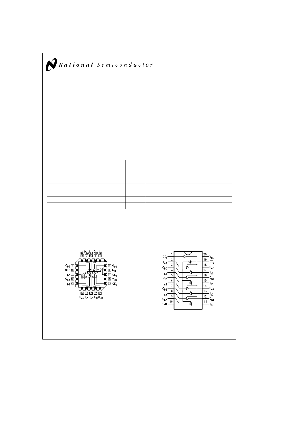
Connection Diagrams
Pin Assignment for LCC
’F2244
TL/F/9499– 3
Pin Assignment for DIP, SOIC and SSOP
’F2244
TL/F/9499– 4
TRI-STATEÉis a registered trademark of National Semiconductor Corporation.
C
1995 National Semiconductor Corporation RRD-B30M105/Printed in U. S. A.

Logic Symbol
IEEE/IEC
’F2244
TL/F/9499– 6
Unit Loading/Fan Out
54F/74F
Pin Names Description
U.L. Input I
IH/IIL
HIGH/LOW Output IOH/I
OL
OE1,OE
2
TRI-STATE Output Enable Input (Active LOW) 1.0/1.667 20 mA/b1mA
OE
2
TRI-STATE Output Enable Input (Active HIGH) 1.0/1.667 20 mA/b1mA
I
an,Ibn
Inputs 1.0/2.667* 20 mA/b1.6 mA
Oan,O
bn
Outputs 750/20
b
15 mA/12 mA
*Worst-case ’F2244 disabled
Truth Table
’F2244
OE
1
I
an
O
an
OE
2
I
bn
O
bn
HXZ HXZ
LHH LHH
LLL LLL
H
e
HIGH Voltage Level
L
e
LOW Voltage Level
X
e
Immaterial
Z
e
High Impedance
2
Absolute Maximum Ratings (Note 1)
If Military/Aerospace specified devices are required,
please contact the National Semiconductor Sales
Office/Distributors for availability and specifications.
Storage Temperature
b
65§Ctoa150§C
Ambient Temperature under Bias
b
55§Ctoa125§C
Junction Temperature under Bias
b
55§Ctoa175§C
Plastic
b
55§Ctoa150§C
V
CC
Pin Potential to
Ground Pin
b
0.5V toa7.0V
Input Voltage (Note 2)
b
0.5V toa7.0V
Input Current (Note 2)
b
30 mA toa5.0 mA
Voltage Applied to Output
in HIGH State (with V
CC
e
0V)
Standard Output
b
0.5V to V
CC
TRI-STATE Output
b
0.5V toa5.5V
Current Applied to Output
in LOW State (Max) twice the rated I
OL
(mA)
ESD Last Passing Voltage (Min) 4000V
Note 1: Absolute maximum ratings are values beyond which the device may
be damaged or have its useful life impaired. Functional operation under
these conditions is not implied.
Note 2: Either voltage limit or current limit is sufficient to protect inputs.
Recommended Operating
Conditions
Free Air Ambient Temperature
Military
b
55§Ctoa125§C
Commercial 0
§
Ctoa70§C
Supply Voltage
Military
a
4.5V toa5.5V
Commercial
a
4.5V toa5.5V
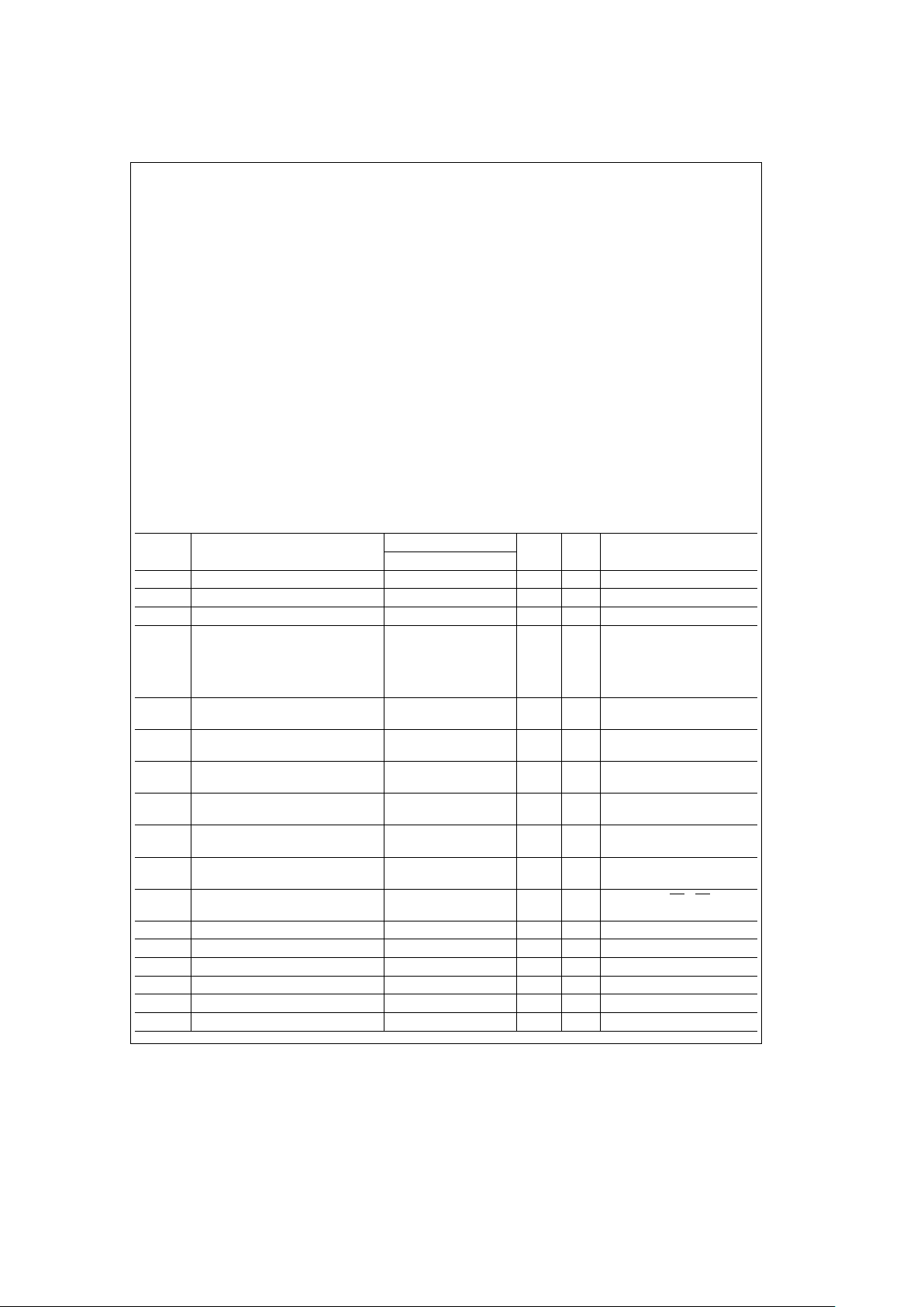
DC Electrical Characteristics
Symbol Parameter
54F/74F
Units V
CC
Conditions
Min Typ Max
V
IH
Input HIGH Voltage 2.0 V Recognized as a HIGH Signal
V
IL
Input LOW Voltage 0.8 V Recognized as a LOW Signal
V
CD
Input Clamp Diode Voltage
b
1.2 V Min I
IN
eb
18 mA
V
OH
Output HIGH 54F 10% V
CC
2.4 I
OH
eb
3mA
Voltage 54F 10% V
CC
2.0 I
OH
eb
12 mA
74F 10% V
CC
2.4
V Min
I
OH
eb
3mA
74F 10% V
CC
2.0 I
OH
eb
15 mA
74F 5% V
CC
2.7 I
OH
eb
3mA
V
OL
Output LOW 0.50
V Min
I
OL
e
1mA
Voltage 0.75 I
OL
e
12 mA
I
IH
Input HIGH 54F 20.0
mA Max V
IN
e
2.7V
Current 74F 5.0
I
BVI
Input HIGH Current 54F 100
mA Max V
IN
e
7.0V
Breakdown Test 74F 7.0
I
CEX
Output HIGH 54F 250
mA Max V
OUT
e
V
CC
Leakage Current 74F 50
V
ID
Input Leakage
74F 4.75 V 0.0
I
ID
e
1.9 mA
Test All other pins grounded
I
OD
Output Leakage
74F 3.75 mA 0.0
V
IOD
e
150 mV
Circuit Current All other pins grounded
I
IL
Input LOW Current
b
1.0
mA Max
V
IN
e
0.5V (OE1,OE2,OE2)
b
1.6 V
IN
e
0.5V (In)
I
OZH
Output Leakage Current 50 mA Max V
OUT
e
2.7V
I
OZL
Output Leakage Current
b
50 mA Max V
OUT
e
0.5V
I
OS
Output Short-Circuit Current
b
100
b
225 mA Max V
OUT
e
0V
I
CCH
Power Supply Current 40 60 mA Max V
O
e
HIGH
I
CCL
Power Supply Current 60 90 mA Max V
O
e
LOW
I
CCZ
Power Supply Current 60 90 mA Max V
O
e
HIGH Z
3
 Loading...