54ABT16374
16-Bit D Flip-Flop with TRI-STATE
®
Outputs
General Description
The ABT16374 contains sixteen non-inverting D flip-flops
with TRI-STATE outputs and is intended for bus oriented applications. The device is byte controlled. A buffered clock
(CP) and Output Enable (OE) are common to each byte and
can be shorted together for full 16-bit operation.
Features
n Separate control logic for each byte
n 16-bit version of the ABT374
n Edge-triggered D-type inputs
n Buffered Positive edge-triggered clock
n High impedance glitch free bus loading during entire
power up and power down cycle
n Non-destructive hot insertion capability
n Guaranteed latch-up protection
n Standard Microcircuit Drawing (SMD) 5962-9320101
Ordering Code:
Commercial Package Package Description
Number
54ABT16374W-QML WA48A 48-Lead Cerpack
Connection Diagram Logic Symbol
Pin Description
Pin Description
Names
OE
n
TRI-STATE Output Enable Input (Active Low)
CP
n
Clock Pulse Input (Active Rising Edge)
D
0–D15
Data Inputs
O
0–O15
TRI-STATE Outputs
TRI-STATE®is a registeredtrademark of National Semiconductor Corporation.
Pin Assignment for Cerpack
DS100224-2
DS100224-1
July 1998
54ABT16374 16-Bit D Flip-Flop with TRI-STATE Outputs
54ABT16374
© 1998 National Semiconductor Corporation DS100224 www.national.com
1
PrintDate=1998/07/14 PrintTime=11:05:34 43604 ds100224 Rev. No. 1 cmserv
Proof 1

Functional Description
The ABT16374 consists of sixteen edge-triggered flip-flops
with individual D-type inputs and TRI-STATE true outputs.
The device is byte controlled with each byte functioningidentically, but independent of the other. The control pins can be
shorted together to obtain full 16-bit operation. Each byte
has a buffered clock and buffered Output Enable common to
all flip-flops within that byte. The description which follows
applies to each byte. Each flip-flop will store the state of their
individual D inputs that meet the setup and hold time requirements on the LOW-to-HIGH Clock (CP
n
) transition. With the
Output Enable (OE
n
) LOW, the contents of the flip-flops are
available at the outputs. When OEnis HIGH, the outputs go
to the high impedance state. Operation of the OEninput
does not affect the state of the flip-flops.
Truth Tables
Inputs Outputs
CP
1
OE
1
D0–D
7
O0–O
7
NL H H
NL L L
L L X (Previous)
XH X Z
Inputs Outputs
CP
2
OE
2
D8–D
15
O8–O
15
NL H H
NL L L
L L X (Previous)
XH X Z
H
=
High Voltage Level
L=Low Voltage Level
X=Immaterial
Z=High Impedance
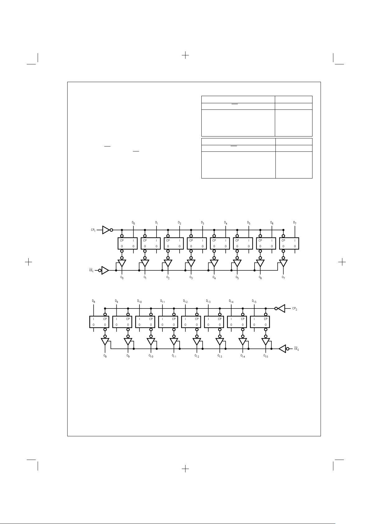
Logic Diagrams
Byte 1 (0:7)
DS100224-3
Byte 2 (8:15)
DS100224-4
PrintDate=1998/07/14 PrintTime=11:05:34 43604 ds100224 Rev. No. 1 cmserv Proof 2
www.national.com 2
 Loading...