NSC 5962-9317502QXA Datasheet

54ABT16245
16-Bit Transceiver with TRI-STATE
®
Outputs
General Description
The ’ABT16245 contains sixteen non-inverting bidirectional
buffers with TRI-STATE outputs and is intended for bus oriented applications. The device is byte controlled. Each byte
has separate control inputs which can be shorted together
for full 16-bit operation. The T/R inputs determine the direction of data flow through the device. The OE inputs disable
both the A and B ports by placing them in a high impedance
state.
Features
n Bidirectional non-inverting buffers
n Separate control logic for each byte
n 16-bit version of the ’ABT245
n A and B output sink capability of 48 mA, source
capability of 24 mA
n Guaranteed latchup protection
n High impedance glitch free bus loading during entire
power up and power down cycle
n Non-destructive hot insertion capability
n Standard Microcircuit Drawing (SMD) 5962-9317501
Military
Package
Number
Package Description
54ABT16245W-QML WA48A 48-Lead Cerpack
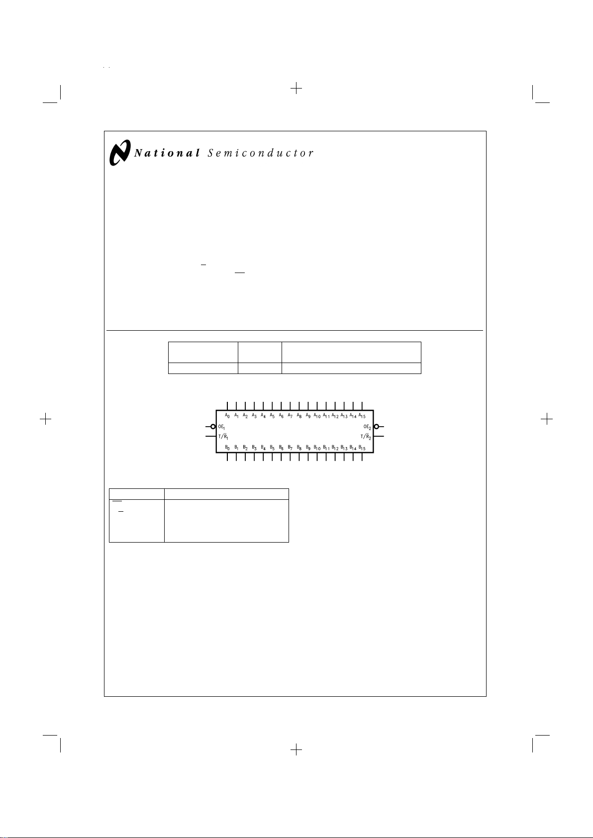
Logic Symbol
Pin Description
Pin Names Description
OE
n
Output Enable Input (Active Low)
T/R
n
Transmit/Receive Input
A
0–A15
Side A Inputs/Outputs
B
0–B15
Side B Inputs/Outputs
TRI-STATE®is a registeredtrademark of National Semiconductor Corporation.
DS100200-1
August 1998
54ABT16245 16-Bit Transceiver with TRI-STATE Outputs
54ABT16245
© 1998 National Semiconductor Corporation DS100200 www.national.com
1
PrintDate=1998/08/27 PrintTime=14:50:42 44961 ds100200 Rev. No. 1 cmserv
Proof 1

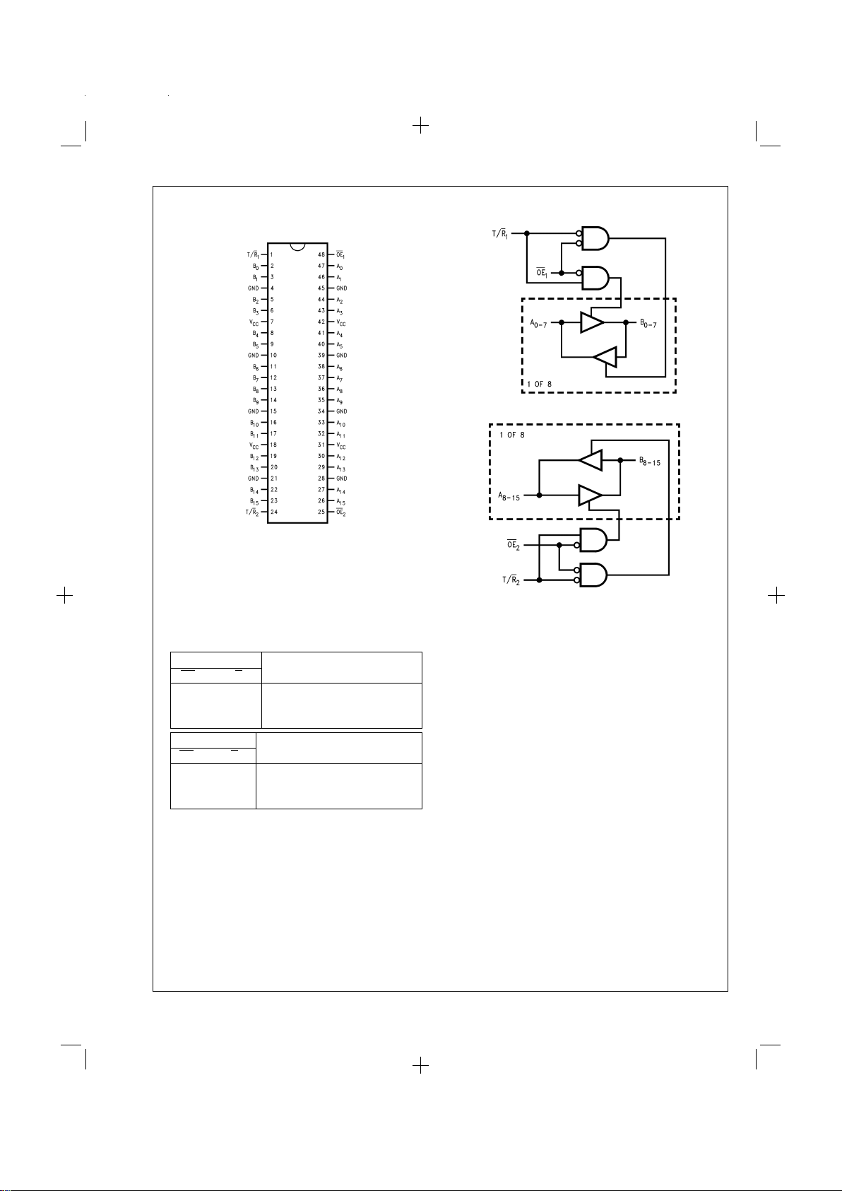
Connection Diagram
Functional Description
The ’ABT16245 contains sixteen non-inverting bidirectional
buffers with TRI-STATE outputs. The device is byte controlled with each byte functioning identically, but independent
of the other. The control pins can be shorted together to obtain full 16-bit operation.
Truth Table
Inputs Outputs
OE
1
T/R
1
L L Bus B0–B7Data to Bus A0–A
7
L H Bus A0–A7Data to Bus B0–B
7
H X HIGH-Z State on A0–A7,B0–B
7
Inputs Outputs
OE
2
T/R
2
L L Bus B8–B15Data to Bus A8–A
15
L H Bus A8–A15Data to Bus B8–B
15
H X HIGH-Z State on A8–A15,B8–B
15
H = High Voltage Level
L = Low Voltage Level
X = Immaterial
Z = High Impedance
Logic Diagrams
Pin Assignment for Cerpack
DS100200-2
DS100200-3
DS100200-4
www.national.com 2
PrintDate=1998/08/27 PrintTime=14:50:42 44961 ds100200 Rev. No. 1 cmserv Proof 2

Absolute Maximum Ratings (Note 1)
If Military/Aerospace specified devices are required,
please contact the National Semiconductor Sales Office/
Distributors for availability and specifications.
Storage Temperature −65˚C to +150˚C
Ambient Temperature under Bias −55˚C to +125˚C
Junction Temperature under Bias
Ceramic −55˚C to +175˚C
V
CC
Pin Potential to
Ground Pin −0.5V to +7.0V
Input Voltage (Note 2) −0.5V to +7.0V
Input Current (Note 2) −30 mA to +5.0 mA
Voltage Applied to Any Output
in the Disabled or
Power-off State −0.5V to 5.5V
in the HIGH State −0.5V to V
CC
Current Applied to Output
in LOW State (Max) twice the rated I
OL
(mA)
DC Latchup Source Current −500 mA
Over Voltage Latchup (I/O) 10V
Recommended Operating
Conditions
Free Air Ambient Temperature
Military −55˚C to +125˚C
Supply Voltage
Military +4.5V to +5.5V
Minimum Input Edge Rate (∆V/∆t)
Data Input 50 mV/ns
Enable Input 20 mV/ns
Note 1: Absolute maximum ratings are valuesbeyond which the device may
be damaged or have its useful life impaired. Functional operation under these
conditions is not implied.
Note 2: Either voltage limit or current limit is sufficient to protect inputs.
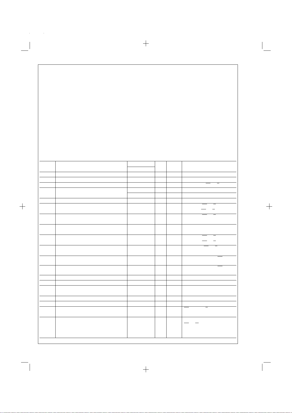
DC Electrical Characteristics
Symbol Parameter ABT16245 Units V
CC
Conditions
Min Typ Max
V
IH
Input HIGH Voltage 2.0 V Recognized HIGH Signal
V
IL
Input LOW Voltage 0.8 V Recognized LOW Signal
V
CD
Input Clamp Diode Voltage −1.2 V Min IIN= −18 mA (OEn, T/Rn)
V
OH
Output HIGH Voltage 54ABT 2.5 V Min IOH=−3mA(An,Bn)
54ABT 2.0 V Min I
OH
= −24 mA (An,Bn)
V
OL
Output LOW Voltage 54ABT 0.55 V Min IOL=48mA(An,Bn)
I
IH
Input HIGH Current 5 µA Max VIN= 2.7V (OEn, T/Rn) (Note 3)
5V
IN=VCC
(OEn, T/Rn)
I
BVI
Input HIGH Current 7 µA Max VIN= 7.0V (OEn, T/Rn)
Breakdown Test
I
BVIT
Input HIGH Current 100 µA Max VIN= 5.5V (An,Bn)
Breakdown Test (I/O)
I
IL
Input LOW Current −5 µA Max VIN= 0.5V (OEn, T/Rn) (Note 3)
−5 VIN= 0.0V (OEn, T/Rn)
V
ID
Input Leakage Test 4.75 V 0.0 IID= 1.9 µA (OEn, T/Rn)
All Other Pins Grounded
I
IH
+I
OZH
Output Leakage Current 50 µA 0 −
5.5V
V
OUT
= 2.7V (An,Bn); OE = 2.0V
IIL+I
OZL
Output Leakage Current −50 µA 0 −
5.5V
V
OUT
= 0.5V (An,Bn); OE = 2.0V
I
OS
Output Short-Circuit Current −100 −275 mA Max V
OUT
= 0.0V (An,Bn)
I
CEX
Output High Leakage Current 50 µA Max V
OUT=VCC(An,Bn
)
I
ZZ
Bus Drainage Test 100 µA 0.0 V
OUT
= 5.50V (An,Bn);
All Others GND
I
CCH
Power Supply Current 100 µA Max All Outputs HIGH
I
CCL
Power Supply Current 60 mA Max All Outputs LOW
I
CCZ
Power Supply Current 100 µA Max OEn=VCC, T/Rn= GND or V
CC
All others at VCCor GND
I
CCT
Additional ICC/Input Outputs Enabled 2.5 mA VI=VCC− 2.1V
Outputs TRI-STATE 2.5 mA Max OE
n
,T/RnVI=VCC− 2.1V
Outputs TRI-STATE 50 µA Data Input VI=VCC− 2.1V
All others at V
CC
or GND
www.national.com3
PrintDate=1998/08/27 PrintTime=14:50:43 44961 ds100200 Rev. No. 1 cmserv Proof 3
 Loading...