

NSC 5962-9314901QSA, 5962-9314901QRA, 5962-9314901Q2A Datasheet
54ABT374
Octal D-Type Flip-Flop with TRI-STATE
®
Outputs
General Description
The ’ABT374 is an octal D-type flip-flop featuring separate
D-type inputs for each flip-flop and TRI-STATE outputs for
bus-oriented applications. Abuffered Clock (CP) and Output
Enable (OE) are common to all flip-flops.
Features
n Edge-triggered D-type inputs
n Buffered positive edge-triggered clock
n TRI-STATE outputs for bus-oriented applications
n Output sink capability of 48 mA, source capability of
24 mA
n Guaranteed multiple output switching specifications
n Output switching specified for both 50 pF and 250 pF
loads
n Guaranteed simultaneous switching, noise level and
dynamic threshold performance
n Guaranteed latchup protection
n High impedance glitch free bus loading during entire
power up and power down cycle
n Non-destructive hot insertion capability
n Standard Microcircuit Drawing (SMD) 5962-9314901
Ordering Code
Military Package Package Description
Number
54ABT374J/883 J20A 20-Lead Ceramic Dual-In-Line
54ABT374W/883 W20A 20-Lead Cerpack
54ABT374E/883 E20A 20-Lead Ceramic Leadless Chip Carrier, Type C
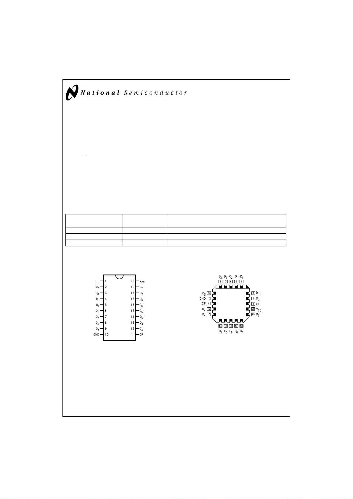
Connection Diagrams
TRI-STATE®is a registered trademark of National Semiconductor Corporation.
Pin Assignment for DIP
and Flatpak
DS100207-1
Pin Assignment
for LCC
DS100207-2
July 1998
54ABT374 Octal D-Type Flip-Flop with TRI-STATE Outputs
© 1998 National Semiconductor Corporation DS100207 www.national.com
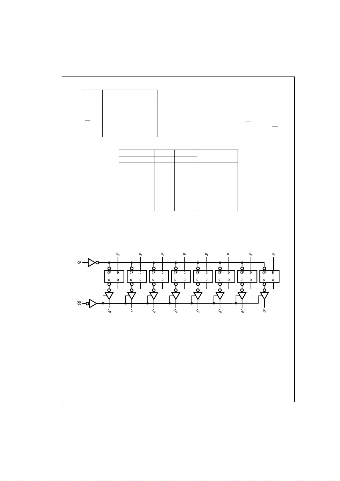
Pin Descriptions
Pin Description
Names
D
0–D7
Data Inputs
CP Clock Pulse Input (Active
Rising Edge)
OE
TRI-STATE Output Enable
Input (Active LOW)
O
0–O7
TRI-STATE Outputs
Functional Description
The ’ABT374 consists of eight edge-triggered flip-flops with
individual D-type inputs and TRI-STATE true outputs. The
buffered clock and buffered Output Enable are common to all
flip-flops. The eight flip-flops will store the state of their individual D inputs that meet the setup and hold time requirements on the LOW-to-HIGH Clock (CP) transition. With the
Output Enable (OE) LOW, the contents of the eight flip-flops
are available at the outputs. When OE is HIGH, the outputs
are in a high impedance state. Operation of the OE input
does not affect the state of the flip-flops.
Function Table
Inputs Internal Outputs Function
OE
CP D Q O
H H L NC Z Hold
H H H NC Z Hold
H
N
L L Z Load
H
N
H H Z Load
L
N
L L L Data Available
L
N
H H H Data Available
L H L NC NC No Change in Data
L H H NC NC No Change in Data
H=HIGH Voltage Level
L=LOW Voltage Level
X=Immaterial
Z=High Impedance
N
=
LOW-to-HIGH Transition
NC=No Change
Logic Diagram
DS100207-3
Please note that this diagram is provided only for the understanding of logic operations and should not be used to estimate propagation delays.
www.national.com 2
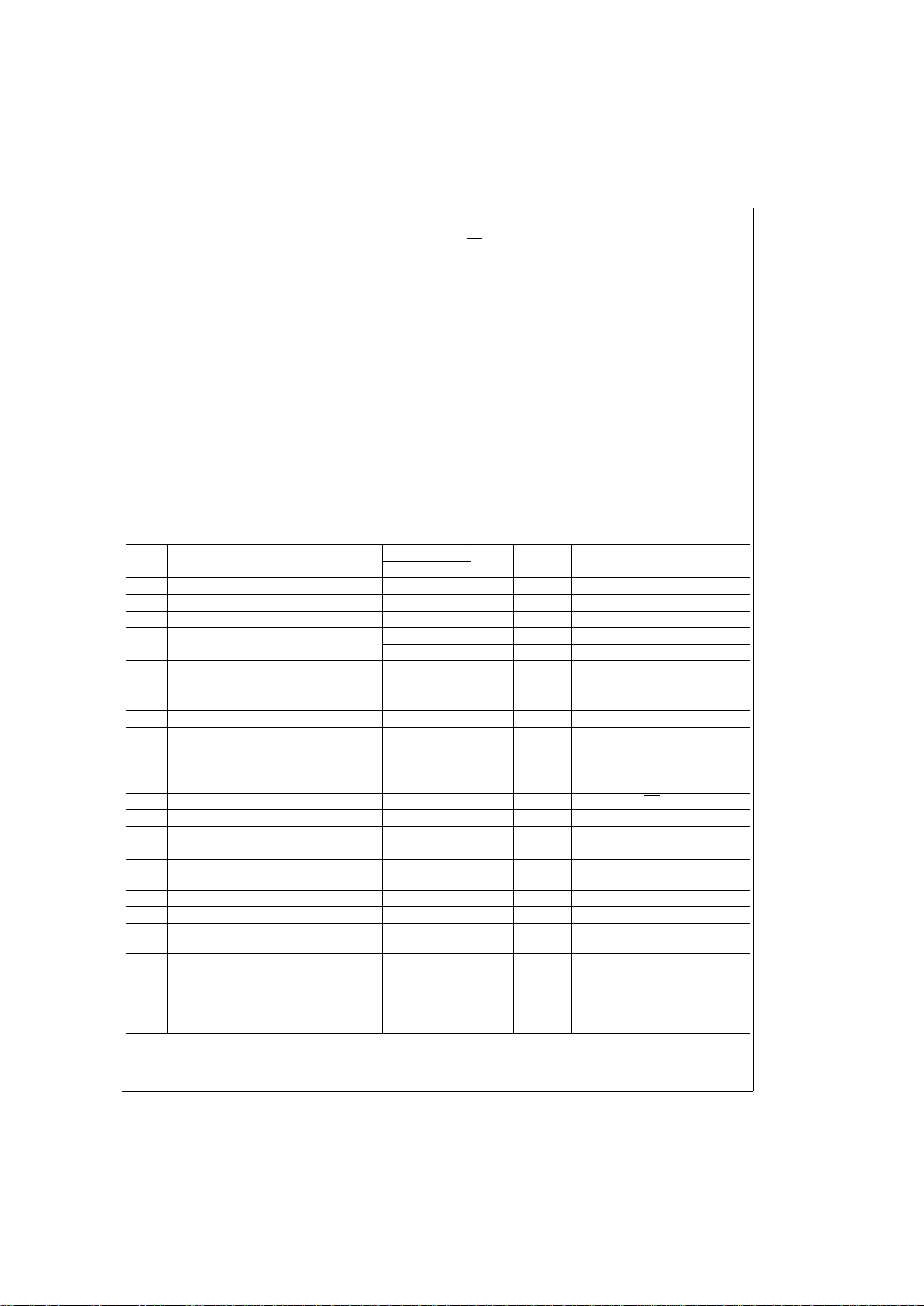
Absolute Maximum Ratings (Note 1)
If Military/Aerospace specified devices are required,
please contact the National Semiconductor Sales Office/
Distributors for availability and specifications.
Storage Temperature −65˚C to +150˚C
Ambient Temperature under Bias −55˚C to +125˚C
Junction Temperature under Bias
Ceramic −55˚C to +175˚C
V
CC
Pin Potential to
Ground Pin −0.5V to +7.0V
Input Voltage (Note 2) −0.5V to +7.0V
Input Current (Note 2) −30 mA to +5.0 mA
Voltage Applied to Any Output
in the Disabled or
Power-Off State −0.5V to 5.5V
in the HIGH State −0.5V to V
CC
Current Applied to Output
in LOW State (Max) twice the rated I
OL
(mA)
DC Latchup Source Current:
OE Pin
−150 mA
(Across Comm Operating Range)
Other Pins −500 mA
Over Voltage Latchup (I/O) 10V
Recommended Operating
Conditions
Free Air Ambient Temperature
Military −55˚C to +125˚C
Supply Voltage
Military +4.5V to +5.5V
Minimum Input Edge Rate (∆V/∆t)
Data Input 50 mV/ns
Enable Input 20 mV/ns
Clock Input 100mV/ns
Note 1: Absolute maximum ratings are values beyond which the device may
be damaged or have its useful life impaired. Functional operation under these
conditions is not implied.
Note 2: Either voltage limit or current limit is sufficient to protect inputs.
DC Electrical Characteristics
Symbol Parameter ABT374 Units V
CC
Conditions
Min Typ Max
V
IH
Input HIGH Voltage 2.0 V Recognized HIGH Signal
V
IL
Input LOW Voltage 0.8 V Recognized LOW Signal
V
CD
Input Clamp Diode Voltage −1.2 V Min I
IN
=
−18 mA
V
OH
Output HIGH 54ABT 2.5 V Min I
OH
=
−3 mA
Voltage 54ABT 2.0 V Min I
OH
=
−24 mA
V
OL
Output LOW Voltage 54ABT 0.55 V Min I
OL
=
48 mA
I
IH
Input HIGH Current 5 µA Max V
IN
=
2.7V (Note 4)
5V
IN
=
V
CC
I
BVI
Input HIGH Current Breakdown Test 7 µA Max V
IN
=
7.0V
I
IL
Input LOW Current −5 µA Max V
IN
=
0.5V (Note 4)
−5 V
IN
=
0.0V
V
ID
Input Leakage Test 4.75 V 0.0 I
ID
=
1.9 µA
All Other Pins Grounded
I
OZH
Output Leakage Current 50 µA 0 − 5.5V V
OUT
=
2.7V; OE=2.0V
I
OZL
Output Leakage Current −50 µA 0 − 5.5V V
OUT
=
0.5V; OE=2.0V
I
OS
Output Short-Circuit Current −100 −275 mA Max V
OUT
=
0.0V
I
CEX
Output High Leakage Current 50 µA Max V
OUT
=
V
CC
I
ZZ
Bus Drainage Test 100 µA 0.0 V
OUT
=
5.5V; All Others V
CC
or
GND
I
CCH
Power Supply Current 50 µA Max All Outputs HIGH
I
CCL
Power Supply Current 30 mA Max All Outputs LOW
I
CCZ
Power Supply Current 50 µA Max OE=VCC; All Others at VCCor
GND
I
CCT
Additional
I
CC
/Input
Outputs Enabled 2.5 mA V
I
=
V
CC
− 2.1V
Outputs TRI-STATE 2.5 mA Max Enable Input V
I
=
V
CC
− 2.1V
Outputs TRI-STATE 2.5 mA Data Input V
I
=
V
CC
− 2.1V
All Others at V
CC
or GND
3 www.national.com
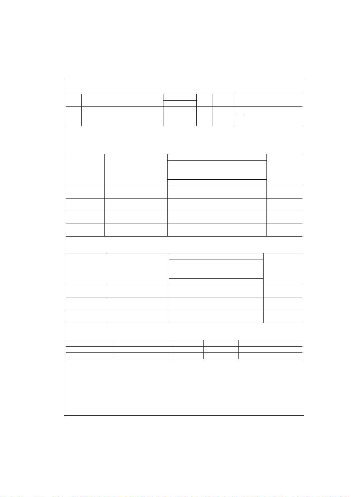
DC Electrical Characteristics (Continued)
Symbol Parameter ABT374 Units V
CC
Conditions
Min Typ Max
I
CCD
Dynamic I
CC
No Load mA/ Max Outputs Open
(Note 4) 0.30 MHz OE=GND, (Note 3)
One Bit Toggling, 50%Duty Cycle
Note 3: For 8-bit toggling, I
CCD
<
0.8 mA/MHz.
Note 4: Guaranteed, but not tested.
AC Electrical Characteristics
Symbol Parameter 54ABT Units
T
A
=
−55˚C to +125˚C
V
CC
=
4.5V to 5.5V
C
L
=
50 pF
Min Max
f
max
Max Clock 150 MHz
Frequency
t
PLH
Propagation Delay 1.4 6.6 ns
t
PHL
CP to O
n
2.0 7.6
t
PZH
Output Enable Time 0.8 5.7 ns
t
PZL
1.5 7.2
t
PHZ
Output Disable Time 1.3 7.2 ns
t
PLZ
1.0 7.0
AC Operating Requirements
54ABT
T
A
=
−55˚C to +125˚C
Symbol Parameter V
CC
=
4.5V to 5.5V Units
C
L
=
50 pF
Min Max
t
s
(H) Setup Time, HIGH 2.5 ns
t
s
(L) or LOW Dnto CP 2.5
t
h
(H) Hold Time, HIGH 2.5 ns
t
h
(L) or LOW Dnto CP 2.5
t
w
(H) Pulse Width, CP 3.3 ns
t
w
(L) HIGH or LOW 3.3
Capacitance
Symbol Parameter Typ Units Conditions (T
A
=
25˚C)
C
IN
Input Capacitance 5.0 pF V
CC
=
0V
C
OUT
(Note 5) Output Capacitance 9.0 pF V
CC
=
5.0V
Note 5: C
OUT
is measured at frequency f=1 MHz, per MIL-STD-883B, Method 3012.
www.national.com 4
 Loading...