

NSC 5962-9232501MXA, 5962-9232501VXA Datasheet
LMD18200
3A, 55V H-Bridge
General Description
The LMD18200 is a 3AH-Bridgedesignedformotioncontrol
applications. Thedeviceis built using a multi-technology process which combines bipolar and CMOS control circuitry
with DMOS power devices on the same monolithic structure.
Ideal for driving DC and stepper motors; the LMD18200 accommodates peak output currents up to 6A. An innovative
circuit which facilitates low-loss sensing of the output current
has been implemented.
Features
n Delivers up to 3A continuous output
n Operates at supply voltages up to 55V
n Low R
DS
(ON) typically 0.3Ω per switch
n TTL and CMOS compatible inputs
n No “shoot-through” current
n Thermal warning flag output at 145˚C
n Thermal shutdown (outputs off) at 170˚C
n Internal clamp diodes
n Shorted load protection
n Internal charge pump with external bootstrap capability
Applications
n DC and stepper motor drives
n Position and velocity servomechanisms
n Factory automation robots
n Numerically controlled machinery
n Computer printers and plotters
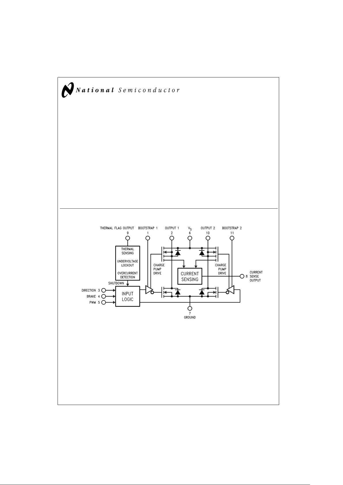
Functional Diagram
DS010568-1
FIGURE 1. Functional Block Diagram of LMD18200
December 1999
LMD18200 3A, 55V H-Bridge
© 1999 National Semiconductor Corporation DS010568 www.national.com
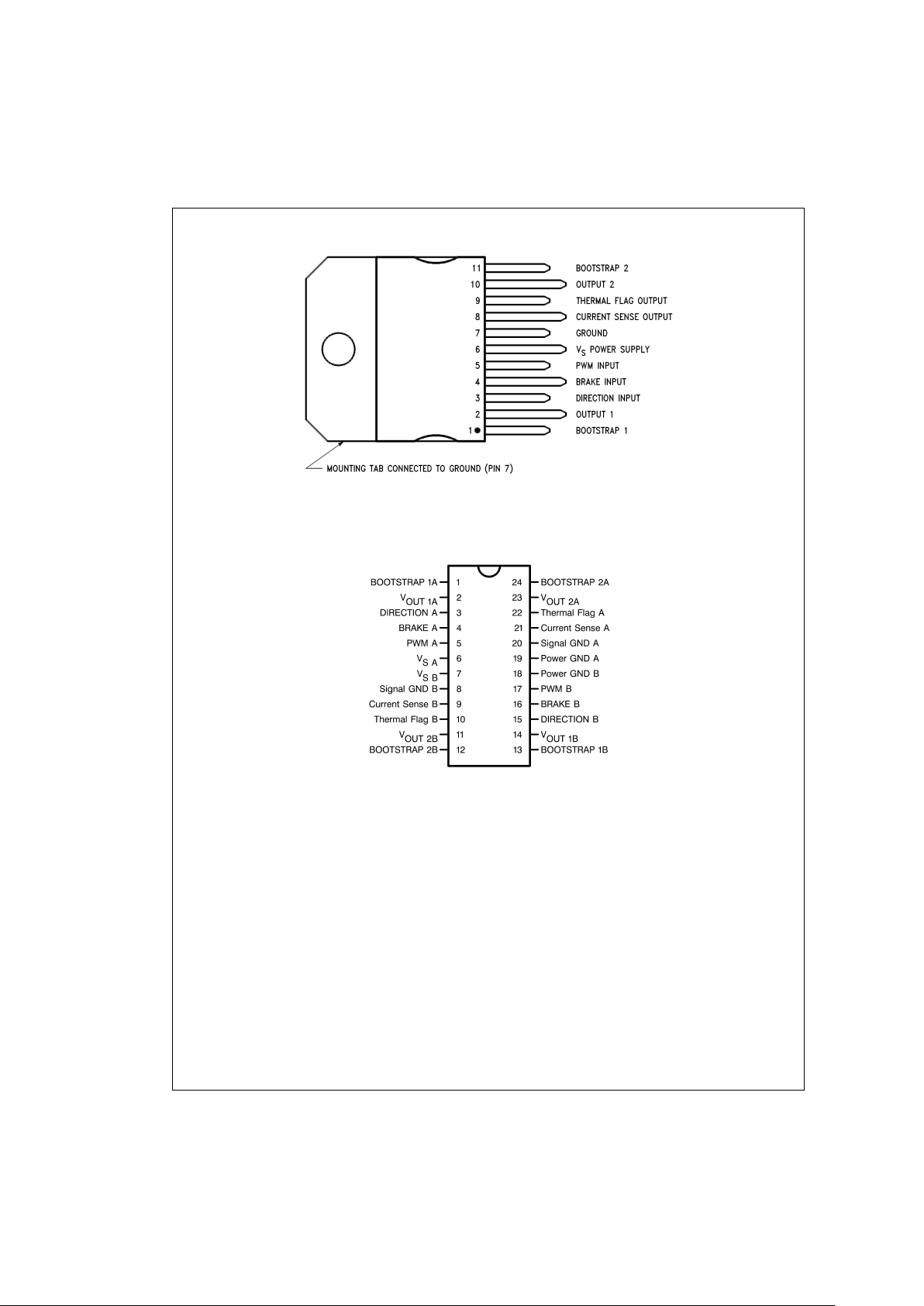
Connection Diagrams and Ordering Information
DS010568-2
11-Lead TO-220 Package
Top View
Order Number LMD18200T
See NS Package TA11B
DS010568-25
24-Lead Dual-in-Line Package
Top View
Order Number LMD18200-2D-QV
5962-9232501VXA
LMD18200-2D/883
5962-9232501MXA
See NS Package DA24B
LMD18200
www.national.com 2

Absolute Maximum Ratings (Note 1)
If Military/Aerospace specified devices are required,
please contact the National Semiconductor Sales Office/
Distributors for availability and specifications.
Total Supply Voltage (V
S
, Pin 6) 60V
Voltage at Pins 3, 4, 5, 8 and 9 12V
Voltage at Bootstrap Pins
(Pins 1 and 11) V
OUT
+16V
Peak Output Current (200 ms) 6A
Continuous Output Current (Note 2) 3A
Power Dissipation (Note 3) 25W
Power Dissipation (T
A
=
25˚C, Free Air) 3W
Junction Temperature, T
J(max)
150˚C
ESD Susceptibility (Note 4) 1500V
Storage Temperature, T
STG
−40˚C to +150˚C
Lead Temperature (Soldering, 10 sec.) 300˚C
Operating Ratings(Note 1)
Junction Temperature, T
J
−40˚C to +125˚C
V
S
Supply Voltage +12V to +55V
Electrical Characteristics (Note 5)
The following specifications apply for V
S
=
42V, unless otherwise specified. Boldface limits apply over the entire operating
temperature range, −40˚C ≤ T
J
≤ +125˚C, all other limits are for T
A
=
T
J
=
25˚C.
Symbol Parameter Conditions Typ Limit Units
R
DS
(ON) Switch ON Resistance Output Current=3A (Note 6) 0.33 0.4/0.6 Ω (max)
R
DS
(ON) Switch ON Resistance Output Current=6A (Note 6) 0.33 0.4/0.6 Ω (max)
V
CLAMP
Clamp Diode Forward Drop Clamp Current=3A (Note 6) 1.2 1.5 V (max)
V
IL
Logic Low Input Voltage Pins 3, 4, 5 −0.1 V (min)
0.8 V (max)
I
IL
Logic Low Input Current V
IN
=
−0.1V, Pins=3, 4, 5 −10 µA (max)
V
IH
Logic High Input Voltage Pins 3, 4, 5 2 V (min)
12 V (max)
I
IH
Logic High Input Current V
IN
=
12V, Pins=3, 4, 5 10 µA (max)
Current Sense Output I
OUT
=
1A (Note 8) 377 325/300 µA (min)
425/450 µA (max)
Current Sense Linearity 1A ≤ I
OUT
≤ 3A (Note 7)
±
6
±
9
%
Undervoltage Lockout Outputs turn OFF 9 V (min)
11 V (max)
T
JW
Warning Flag Temperature Pin 9 ≤ 0.8V, I
L
=
2 mA 145 ˚C
V
F
(ON) Flag Output Saturation Voltage T
J
=
T
JW,IL
=
2 mA 0.15 V
I
F
(OFF) Flag Output Leakage V
F
=
12V 0.2 10 µA (max)
T
JSD
Shutdown Temperature Outputs Turn OFF 170 ˚C
I
S
Quiescent Supply Current All Logic Inputs Low 13 25 mA (max)
t
Don
Output Turn-On Delay Time Sourcing Outputs, I
OUT
=
3A 300 ns
Sinking Outputs, I
OUT
=
3A 300 ns
t
on
Output Turn-On Switching Time Bootstrap Capacitor=10 nF
Sourcing Outputs, I
OUT
=
3A 100 ns
Sinking Outputs, I
OUT
=
3A 80 ns
t
Doff
Output Turn-Off Delay Times Sourcing Outputs, I
OUT
=
3A 200 ns
Sinking Outputs, I
OUT
=
3A 200 ns
t
off
Output Turn-Off Switching Times Bootstrap Capacitor=10 nF
Sourcing Outputs, I
OUT
=
3A 75 ns
Sinking Outputs, I
OUT
=
3A 70 ns
t
pw
Minimum Input Pulse Width Pins 3, 4 and 5 1 µs
t
cpr
Charge Pump Rise Time No Bootstrap Capacitor 20 µs
LMD18200
www.national.com3
Electrical Characteristics Notes
Note 1: Absolute Maximum Ratings indicate limits beyond which damage to the device may occur. DC and AC electrical specifications do not apply when op-
erating the device beyond its rated operating conditions.
Note 2: See Application Information for details regarding current limiting.
Note 3: The maximum power dissipation must be derated at elevated temperatures and is a function of T
J(max)
, θJA, and TA. The maximum allowable power dis-
sipation at any temperature is P
D(max)
=
(T
J(max)−TA
)/θJA, or the number given in the Absolute Ratings, whichever is lower. The typical thermal resistance from junc-
tion to case (θ
JC
) is 1.0˚C/W and from junction to ambient (θJA) is 30˚C/W. For guaranteed operation T
J(max)
=
125˚C.
Note 4: Human-body model, 100 pF discharged through a 1.5 kΩ resistor. Except Bootstrap pins (pins 1 and 11) which are protected to 1000V of ESD.
Note 5: All limits are 100%production tested at 25˚C. Temperature extreme limits are guaranteed via correlation using accepted SQC (Statistical Quality Control)
methods. All limits are used to calculate AOQL, (Average Outgoing Quality Level).
Note 6: Output currents are pulsed (t
W
<
2 ms, Duty Cycle<5%).
Note 7: Regulation is calculated relative to the current sense output value with a 1A load.
Note 8: Selections for tighter tolerance are available. Contact factory.
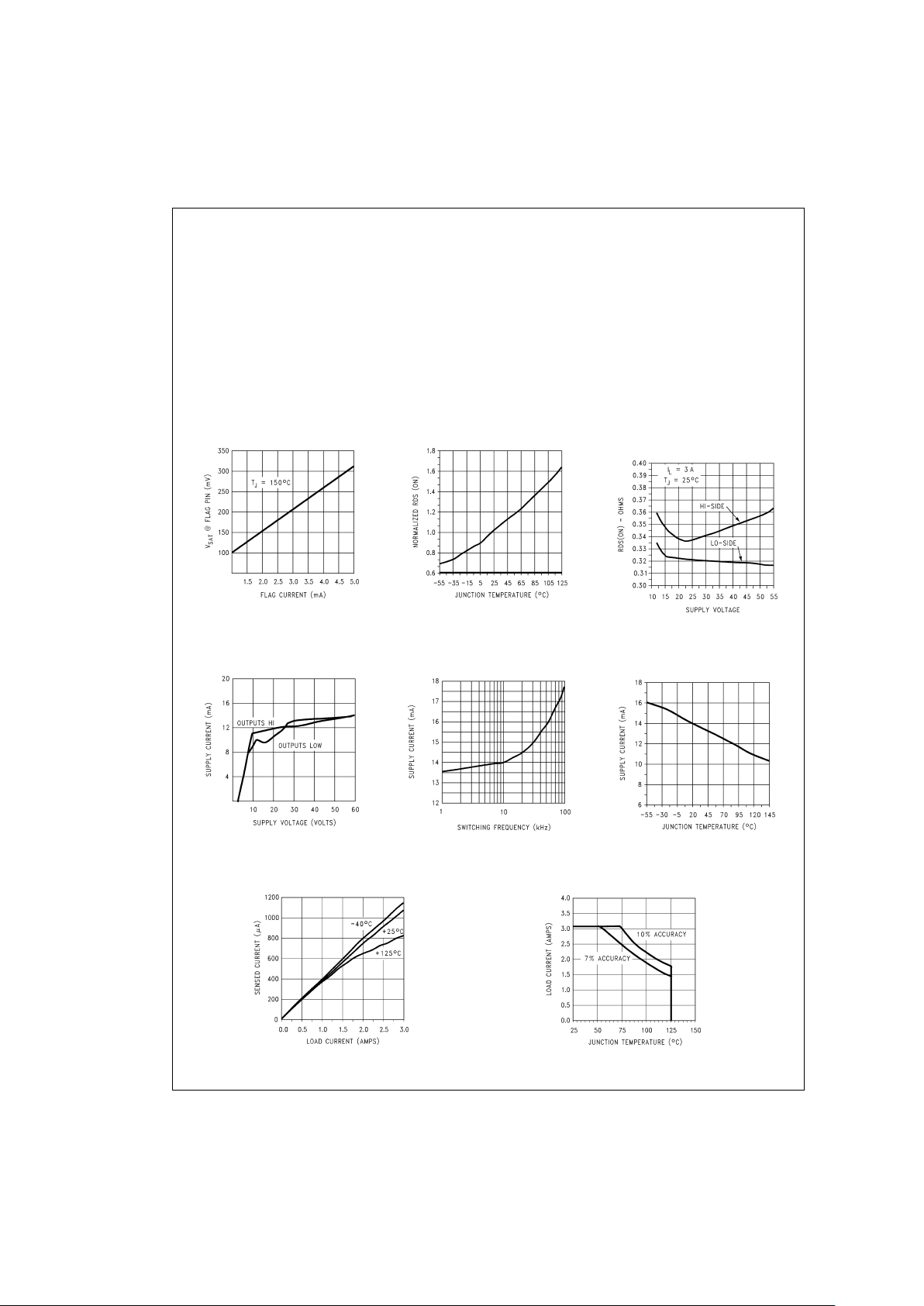
Typical Performance Characteristics
V
SAT
vs Flag Current
DS010568-16
RDS(ON) vs Temperature
DS010568-17
RDS(ON) vs
Supply Voltage
DS010568-18
Supply Current vs
Supply Voltage
DS010568-19
Supply Current vs
Frequency (V
S
=
42V)
DS010568-20
Supply Current vs
Temperature (V
S
=
42V)
DS010568-21
Current Sense Output
vs Load Current
DS010568-22
Current Sense
Operating Region
DS010568-23
LMD18200
www.national.com 4
 Loading...