NSC 5962-9153101VYA, 5962-9153101VXA, 5962-9153101MYA, 5962-9153101MXA, 100325MW8 Datasheet

100325
Low Power Hex ECL-to-TTL Translator
General Description
The 100325 is a hex translator for converting F100K logic
levels to TTLlogiclevels.Differentialinputsalloweachcircuit
to be used as an inverting, non-inverting or differential receiver.An internal reference voltage generator provides V
BB
for single-ended operation, or for use in Schmitt trigger applications. All inputs have 50 kΩ pull-down resistors.When the
inputs are either unconnected or at the same potential the
outputs will go low.
When used in single-ended operation the apparent input
threshold of the true inputs is 20 mV to 40 mV higher (positive) than the threshold of the complementary inputs. The
V
EE
and V
TTL
power may be applied in either order.
Features
n Pin/function compatible with 100125
n Meets 100125 AC specifications
n 50%power reduction of the 100125
n Differential inputs with built in offset
n Standard FAST
®
outputs
n 2000V ESD protection
n −4.2V to −5.7V operating range
n Available to Microcircuit Drawing
(SMD) 5962-9153101
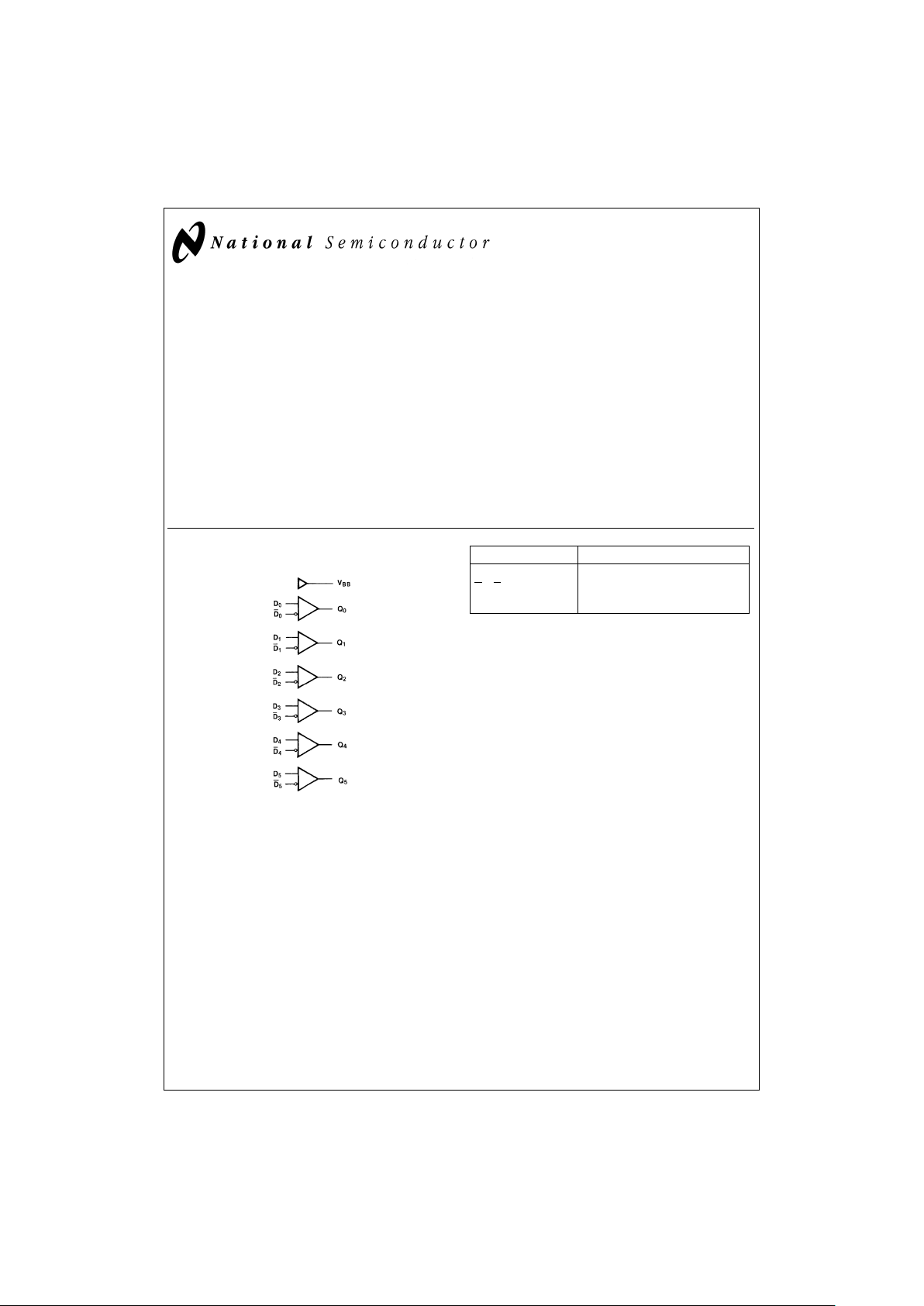
Logic Diagram
Pin Names Description
D
0–D5
Data Inputs
D
0–D5
Inverting Data Inputs
Q
0–Q5
Data Outputs
FAST®is a registered trademark of FairchildSemiconductor.
DS100314-4
August 1998
100325 Low Power Hex ECL-to-TTL Translator
© 1998 National Semiconductor Corporation DS100314 www.national.com

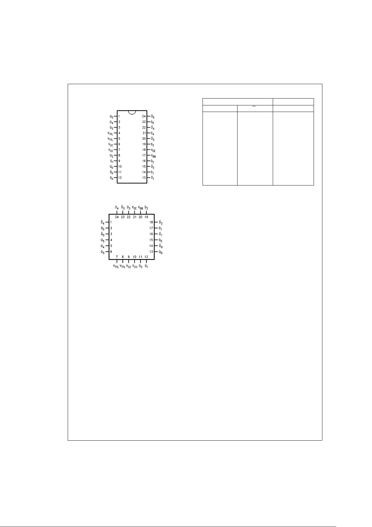
Connection Diagrams Truth Table
Inputs Outputs
D
n
D
n
Q
n
LH L
HL H
LL L
HH L
Open Open L
V
EE
V
EE
L
LV
BB
L
HV
BB
H
V
BB
LH
V
BB
HL
H
=
HIGH Voltage Level
L=LOW Voltage Level
24-Pin DIP
DS100314-1
24-Pin Quad Cerpak
DS100314-2
www.national.com 2

Absolute Maximum Ratings (Note 1)
If Military/Aerospace specified devices are required,
please contact the National Semiconductor Sales Office/
Distributors for availability and specifications.
Above which the useful life may be impaired.
Storage Temperature (T
STG
) −65˚C to +150˚C
Maximum Junction Temperature (T
J
)
Ceramic +175˚C
V
EE
Pin Potential to Ground Pin −7.0V to +0.5V
V
TTL
Pin Potential to Ground Pin −0.5V to +6.0V
Input Voltage (DC) V
EE
to +0.5V
Voltage Applied to Output
in HIGH State (with V
CC
=
0V) −0.5V to V
CC
Current Applied to Output
in LOW State (Max) twice the rated I
OL
(mA)
ESD (Note 2) ≥2000V
Recommended Operating
Conditions
Case Temperature (TC)
Military −55˚C to +125˚C
Supply Voltage (V
EE
) −5.7V to −4.2V
Note 1: Absolute maximum ratings are those values beyond which the device may be damaged or have its useful life impaired. Functional operation
under these conditions is not implied.
Note 2: ESD testing conforms to MIL-STD-883, Method 3015.
Military Version
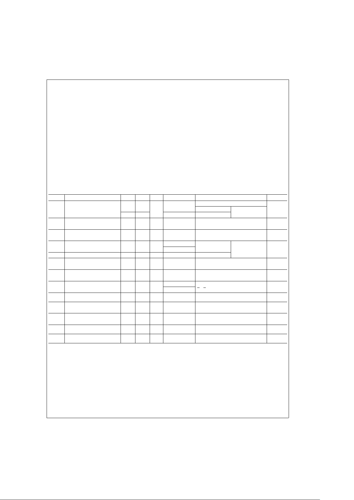
DC Electrical Characteristics
V
EE
=
−4.2V to −5.7V, V
CC
=
V
CCA
=
GND, T
C
=
−55˚C to +125˚C, C
L
=
50 pF, V
TTL
=
+4.5V to +5.5V
Symbol Parameter Min Max Units T
C
Conditions Notes
V
BB
Output Reference Voltage −1380 −1260 0˚C to +125˚C I
VBB
=
−3 µA, V
EE
=
−4.2V
(Notes 3,
4, 5)
mV I
VBB
=
−2.1 mA V
EE
=
−5.7V
−1396 −1260 −55˚C I
VBB
=
−3 mA
V
IH
Input HIGH Voltage −1165 −870 mV −55˚C to +125˚C Guaranteed HIGH Signal for All Inputs
(Notes 3,
4, 5, 6)
(with One Input Tied to V
BB
)
V
IL
Input LOW Voltage −1830 −1475 mV −55˚C to +125˚C Guaranteed LOW Signal for All Inputs
(Notes 3,
4, 5, 6)
(with One Input Tied to V
BB
)
V
OH
Output HIGH Voltage 2.5 mV 0˚C to +125˚C I
OH
=
−2.0 mA V
IN
=
V
IH (Max)
(Notes 3,
4, 5)
2.4 −55˚C or V
IL (Min)
V
OL
Output LOW Voltage 0.5 mV −55˚C to +125˚C I
OL
=
20 mA
V
DIFF
Input Voltage Differential 150 mV −55˚C to +125˚C Required for Full Output Swing
(Notes 3,
4, 5)
V
CM
Common Mode Voltage −2000 −500 mV −55˚C to +125˚C
(Notes 3,
4, 5, 6)
I
IH
Input HIGH Current 350 µA 0˚C to +125˚C V
IN
=
V
IH (Max),D0–D5
=
V
BB
,
(Notes 3,
4, 5)
500 −55˚C D
0–D5
=
V
IL (Min)
I
IL
Input LOW Current 0.50 µA −55˚C to +125˚C V
IN
=
V
IL (Min),D0–D5
=
V
BB
(Notes 3,
4, 5)
I
OS
Output Short Circuit −150 −60 mA −55˚C to +125˚C V
OUT
=
GND
(Notes 3,
4, 5)
Current Test One Output at a Time
I
CEX
Output HIGH 250 µA −55˚C to +125˚C V
OUT
=
5.5V
(Notes 3,
4, 5)
Leakage Current
I
EE
VEEPower Supply Current −35 −12 mA −55˚C to +125˚C D0–D
5
=
V
BB
(Notes 3,
4, 5)
I
TTL
V
TTL
Power Supply Current 65 mA −55˚C to +125˚C D0–D
5
=
V
BB
(Notes 3,
4, 5)
Note 3: F100K 300 Series cold temperature testing is performed by temperature soaking (to guarantee junction temperature equals −55˚C), then testing immediately
without allowing for the junction temperature to stabilize due to heat dissipation after power-up. This provides “cold start” specs which can be considered a worst case
condition at cold temperatures.
Note 4: Screen tested 100%on each device at −55˚C, +25˚C, and +125˚C, Subgroups 1, 2, 3, 7, and 8.
Note 5: Sample tested (Method 5005, Table I) on each manufactured lot at −55˚C, + 25˚C, and +125˚C, SubgroupsA1, 2, 3, 7, and 8.
Note 6: Guaranteed by applying specified input condition and testing V
OH/VOL
.
3 www.national.com
 Loading...