

Page 1
Page 2

RM-84/99
Nokia Customer Care RF Troubleshooting and Manual Tuning Guide
(This page left intentionally blank.)
Page 1–2 Company Confidential Issue 1
Copyright ©2005 Nokia. All Rights Reserved.
Page 3
RM-84/99
RF Troubleshooting and Manual Tuning Guide Nokia Customer Care
Table of Contents
Introduction to RF troubleshooting..........................................................................................................................................1–5
RF key component placement.....................................................................................................................................................1–5
Troubleshooting test point locations.......................................................................................................................................1–7
Receiver troubleshooting...........................................................................................................................................................1–10
Introduction to Rx troubleshooting..................................................................................................................................1–10
GSM Rx chain activation for manual measurements / GSM RSSI measurement.................................................1–10
WCDMA Rx chain activation for manual measurement..............................................................................................1–11
WCDMA RSSI measurement..................................................................................................................................................1–12
Transmitter troubleshooting....................................................................................................................................................1–13
General instructions for Tx troubleshooting..................................................................................................................1–13
Checking antenna functionality.........................................................................................................................................1–16
RF tunings.......................................................................................................................................................................................1–17
Introduction to RF tunings...................................................................................................................................................1–17
RF autotuning..........................................................................................................................................................................1–18
RF autotuning....................................................................................................................................................................1–18
RF manual tuning guide.......................................................................................................................................................1–23
Required manual tunings after component changes...........................................................................................1–23
System mode independent manual tunings............................................................................................................1–24
RF channel filter calibration.....................................................................................................................................1–24
PA (power amplifier) detection..............................................................................................................................1–25
Temperature sensor calibration ............................................................................................................................1–25
GSM receiver tunings.......................................................................................................................................................1–26
Rx calibration (GSM)...................................................................................................................................................1–26
Rx band filter response compensation (GSM)....................................................................................................1–30
Rx AM suppression (GSM)..........................................................................................................................................1–36
GSM transmitter tunings.................................................................................................................................................1–39
Tx IQ tuning (GSM)......................................................................................................................................................1–39
Tx power level tuning (GSM)....................................................................................................................................1–42
RM-84 WCDMA receiver tunings....................................................................................................................................1–45
Rx AGC alignment (WCDMA).....................................................................................................................................1–45
Rx band response calibration (WCDMA)...............................................................................................................1–47
RM-84 WCDMA transmitter tunings.............................................................................................................................1–50
Tx AGC & power detector (WCDMA).......................................................................................................................1–50
Tx band response calibration (WCDMA)...............................................................................................................1–55
Tx LO leakage (WCDMA).............................................................................................................................................1–56
List of Tables
Table 1 RF channel filter calibration tuning limits.............................................................................................................1–24
Table 2 Temperature sensor calibration tuning limits.....................................................................................................1–26
Table 3 RF tuning limits in Rx calibration.............................................................................................................................1–28
Table 4 RSSI level values.............................................................................................................................................................1–38
List of Figures
Figure 1 RF key component placement....................................................................................................................................1–6
Figure 2 Test point locations for spectrum analyzer...........................................................................................................1–7
Figure 3 Test points for oscilloscope - bottom......................................................................................................................1–8
Figure 4 Test points for oscilloscope - top..............................................................................................................................1–9
Figure 5 RSSI Reading window.................................................................................................................................................1–11
Issue 1 Company Confidential Page 1–3
Copyright ©2005 Nokia. All Rights Reserved.
Page 4
RM-84/99
Nokia Customer Care RF Troubleshooting and Manual Tuning Guide
Figure 6 Activating Rx Control window in Phoenix...........................................................................................................1–11
Figure 7 Rx Control window......................................................................................................................................................1–12
Figure 8 RF Controls window....................................................................................................................................................1–15
Figure 9 Tx Control window......................................................................................................................................................1–16
Figure 10 Feed and GND spots of the main antenna.........................................................................................................1–17
Figure 11 BT antenna..................................................................................................................................................................1–17
Figure 12 RF channel filter calibration typical values.......................................................................................................1–25
Figure 13 High burst measurement........................................................................................................................................1–53
Page 1–4 Company Confidential Issue 1
Copyright ©2005 Nokia. All Rights Reserved.
Page 5
RM-84/99
RF Troubleshooting and Manual Tuning Guide Nokia Customer Care
Introduction to RF troubleshooting
All measurements should be done using:
• spectrum analyser with a high-frequency high-impedance passive probe (LO-/reference frequencies and RF
power levels)
• oscilloscope with a 10:1 probe (DC-voltages and low frequency signals)
Caution: A mobile phone WCDMA transmitter should never be tested with full Tx power, if there is no
possibility to perform the measurements in a good performance RF-shielded room. Even low power
WCDMA transmitters may disturb nearby WCDMA networks and cause problems to 3G cellular phone
communication in wide area. WCDMA Tx measurements should be performed at least in an RF-shielded
box and never with higher Tx power level than 0 dBm! Test full WCDMA Tx power only in RF-shielded
environment.
Also all measurements with an RF coupler should be performed in RF shielded environment because
nearby base stations can disturb sensitive receiver measurements. If there is no possibility to use RF
shielded environment, it should be checked that there are no transmissions on the same frequencies
as used in the tests.
The RF section of the phone is build around two RF ASICS: Rx ASIC N7500 and Tx ASIC N7501. There are also two
PA’s on board, one for GSM (N7502) and another for WCDMA (N7503).
The WCDMA PA needs variable supply voltage to work properly and therefore there is a switched mode power
supply component (N7504) added to the PWB.
Please note that the grounding of the PA module is directly below the PA module. Therefore, it is difficult to
check or change the module.
Most RF semiconductors are static discharge sensitive! ESD protection must be taken care of during repair
(ground straps and ESD soldering irons). N7501, N7500, both PAs and SMPS are moisture sensitive, so parts must
be pre-baked prior to soldering.
In addition to key components, there are lot of discrete components (resistors, inductors and capacitors) which
troubleshooting is done mainly by checking if the soldering of the component is done properly.
Capacitor can be checked for shorts and resistors for value by means of an ohmmeter, but be aware in-circuit
measurements should be evaluated carefully.
Keep in mind that all measured voltages or RF levels depicted in the service manual are rough figures. Especially
RF levels vary because of different measuring equipment or different grounding of the probe used. All spectrum
analyser measurements in this manual are made with a Fluke PM9639/011 10:1 (500 ohm) probe. It is
recommended that a similar kind of probe is used for all troubleshooting measurements.
When using an RF probe, use a pair of metallic tweezers to connect the probe ground to the PWB ground as
close to the measurement point as possible. If measurements are performed in a product specific module jig,
then “GND” pads should be used for the probe ground.
For additional RF troubleshooting instructions, see Appendix A. These instructions include descriptions/
instructions for RF self-tests as well as troubleshooting instructions for various fault cases.
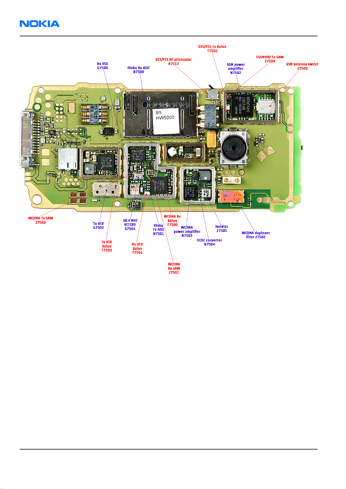
RF key component placement
The RF section of the phone is build around two RF ASICs: Rx ASIC N7500 and Tx ASIC N7501.
There are also two PAs on the board, one for GSM (N7502) and one for WCDMA (N7503). The WCDMA PA needs
variable supply voltage to work power efficiently and therefore there is a Switched Mode Power Supply (SMPS)
component (N7504) added to the PWB.
Issue 1 Company Confidential Page 1–5
Copyright ©2005 Nokia. All Rights Reserved.
Page 6
RM-84/99
Nokia Customer Care RF Troubleshooting and Manual Tuning Guide
Figure 1 RF key component placement
Page 1–6 Company Confidential Issue 1
Copyright ©2005 Nokia. All Rights Reserved.
Page 7
RM-84/99
RF Troubleshooting and Manual Tuning Guide Nokia Customer Care
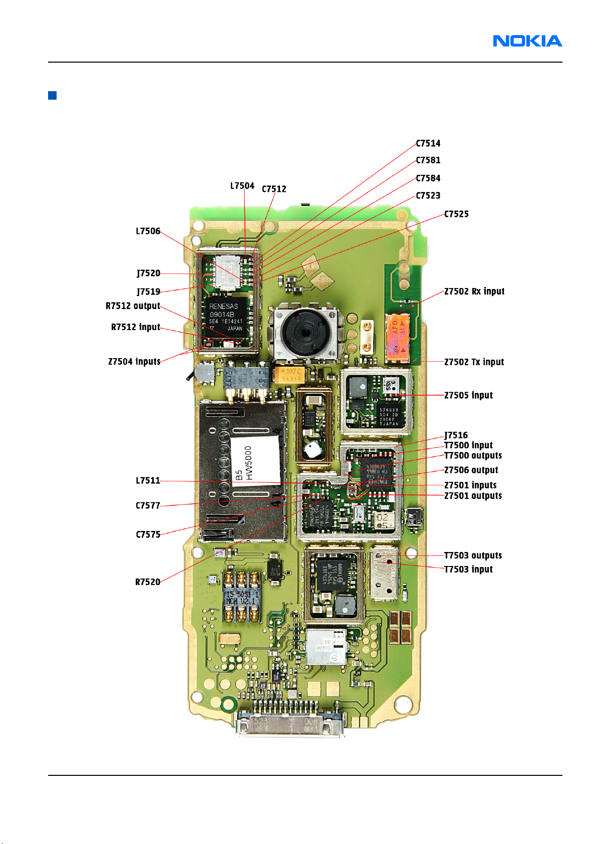
Troubleshooting test point locations
Test points for spectrum analyzer
Figure 2 Test point locations for spectrum analyzer
Issue 1 Company Confidential Page 1–7
Copyright ©2005 Nokia. All Rights Reserved.
Page 8
RM-84/99
Nokia Customer Care RF Troubleshooting and Manual Tuning Guide
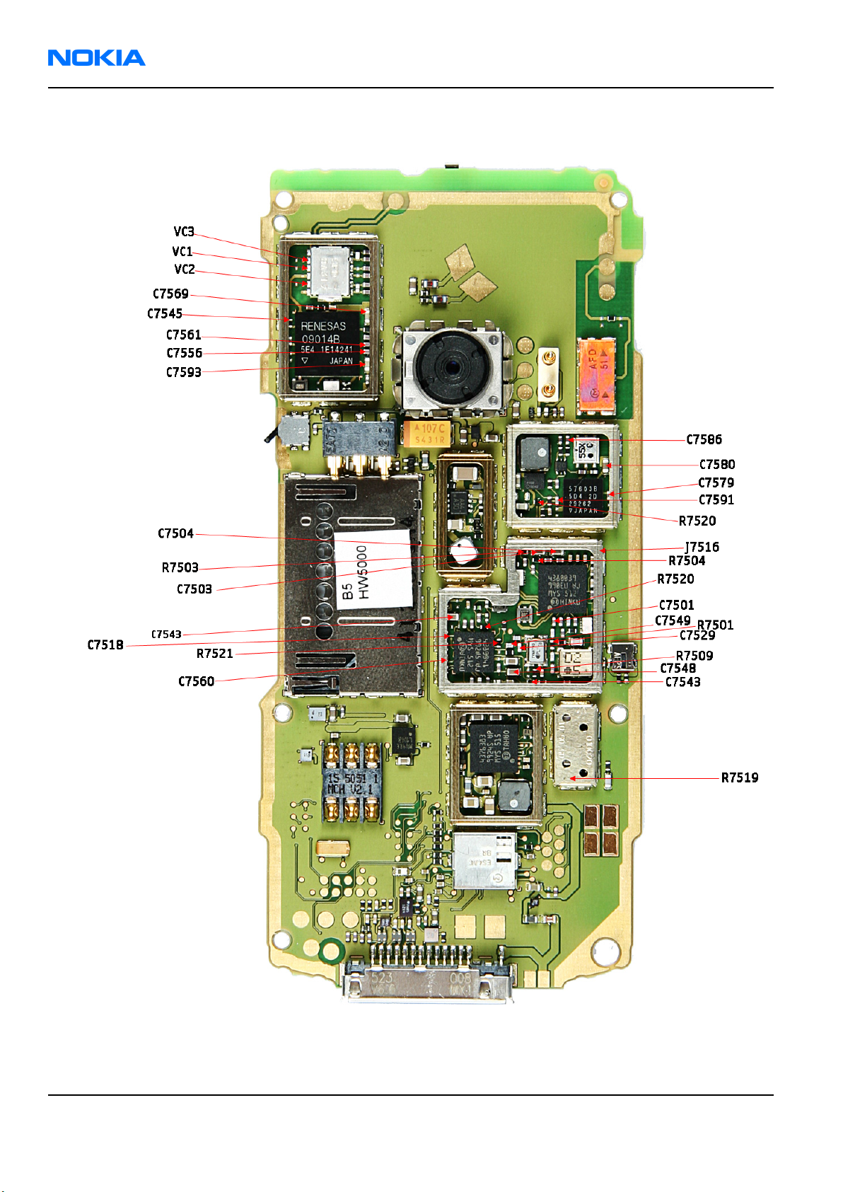
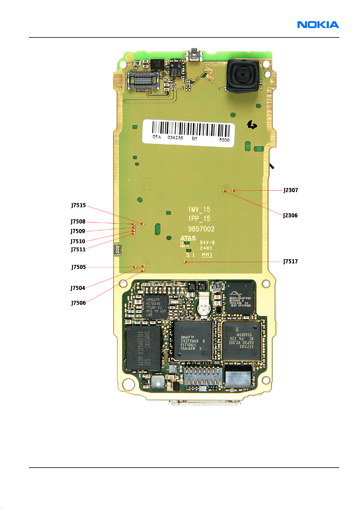
Test points for oscilloscope
Figure 3 Test points for oscilloscope - bottom
Page 1–8 Company Confidential Issue 1
Copyright ©2005 Nokia. All Rights Reserved.
Page 9
RM-84/99
RF Troubleshooting and Manual Tuning Guide Nokia Customer Care
Figure 4 Test points for oscilloscope - top
Issue 1 Company Confidential Page 1–9
Copyright ©2005 Nokia. All Rights Reserved.
Page 10
RM-84/99
Nokia Customer Care RF Troubleshooting and Manual Tuning Guide
Receiver troubleshooting
Introduction to Rx troubleshooting
Rx can be tested by making a phone call or in the local mode. For the local mode testing, use Phoenix service
software.
The main Rx troubleshooting measurement is RSSI measurement. This test measures the signal strength of the
received signal. I and Q branches can be measured separately. For GSM RSSI measurement, see GSM Rx chain
activation for manual measurements / GSM RSSI measurement (Page 1–10), and for the same measurement
in WCDMA, see WCDMA RSSI measurement (Page 1–12).
In GSM, the input signal can be either a real GSM signal or a CW signal that is 67.771kHz up from the carrier
frequency.
For service tool usage instructions, refer to section Service Tools and Service Concepts.
See Also
• WCDMA Rx chain activation for manual measurement (Page 1–11)
GSM Rx chain activation for manual measurements / GSM RSSI measurement
Context
RSSI signal measurement is the main Rx troubleshooting measurement. The test measures the strength of the
received signal.
I and Q branches can be measured separately. In GSM, the input signal can be either real GSM signal or CW signal
that is 67.771kHz up from the carrier frequency.
Steps
1. Start Phoenix service software.
2. From the Testing menu, choose GSM and RSSI Reading.
3. Set the RF signal generator for channel frequency +67.771kHz CW mode with –80dBm signal.
Alternatively set cellular tester downlink channel to the appropriate channel.
Page 1–10 Company Confidential Issue 1
Copyright ©2005 Nokia. All Rights Reserved.
Page 11
RM-84/99
RF Troubleshooting and Manual Tuning Guide Nokia Customer Care
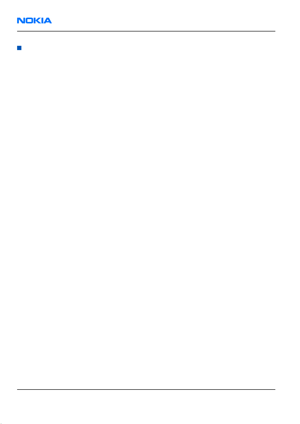
4. In the RSSI Reading window, select the appropriate band and channel.
Figure 5 RSSI Reading window
5. To start measurement/activate GSM Rx chain, click the Start button.
Results
RSSI reading values of the selected band and channel are displayed.
WCDMA Rx chain activation for manual measurement
Steps
1. Start Phoenix service software.
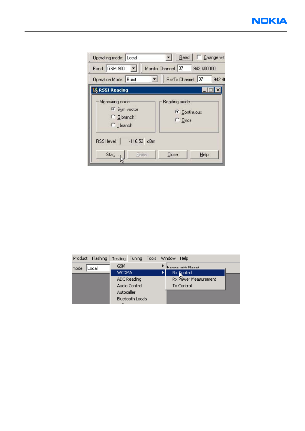
2. From the Testing menu, choose WCDMA and Rx Control.
Figure 6 Activating Rx Control window in Phoenix
3. In the Rx Control window:
Issue 1 Company Confidential Page 1–11
Copyright ©2005 Nokia. All Rights Reserved.
Page 12
RM-84/99
Nokia Customer Care RF Troubleshooting and Manual Tuning Guide
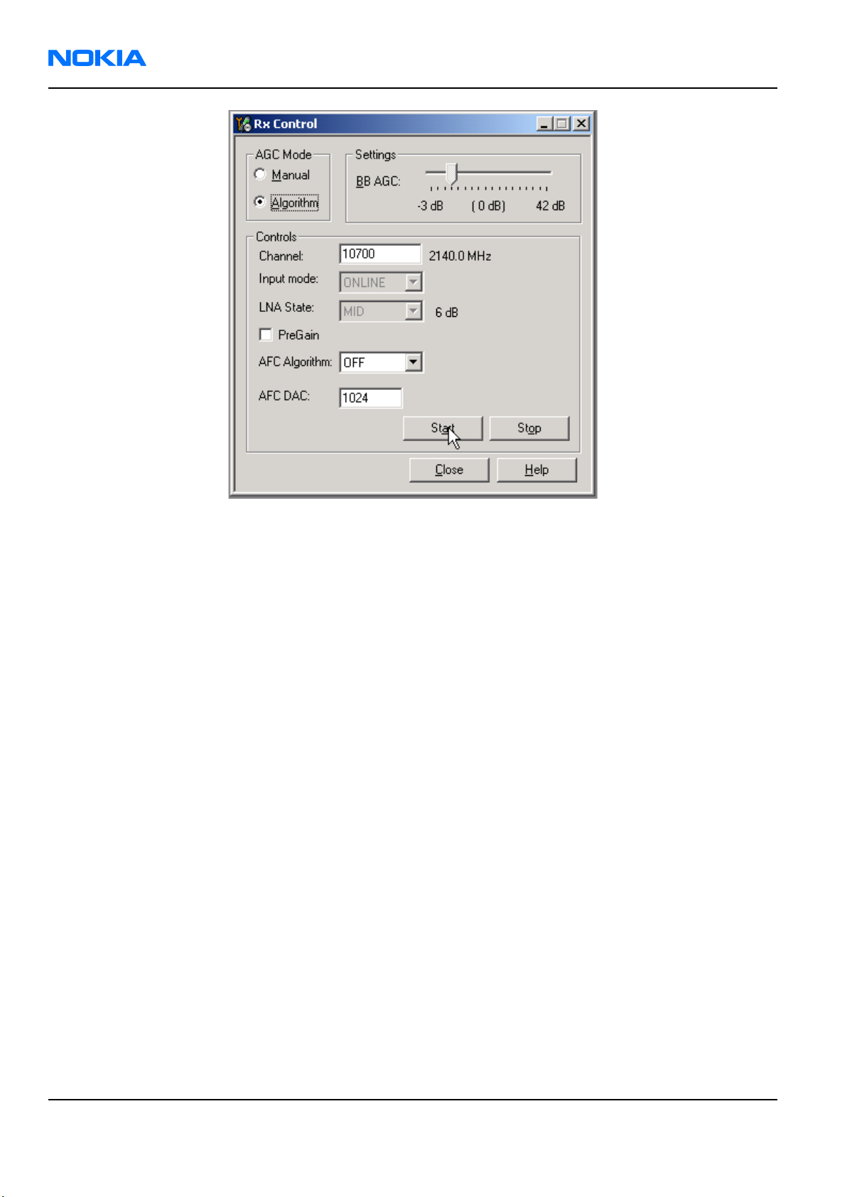
Figure 7 Rx Control window
• From the AGC Mode pane, select Algorithm.
• Set Channel to 10700.
• Set AFC Algorithm to OFF (Default = OFF).
Next action
When settings are ready, click Start to activate them.
If settings are changed later on (for example, you give a new channel number), you will need to click Stop and
Start again.
Note: Clicking Stop also disables Tx Control if that was active!
WCDMA RSSI measurement
Before you begin
WCDMA Rx must be activated before RSSI can be measured. See WCDMA Rx chain activation for manual
measurement (Page 1–11).
Steps
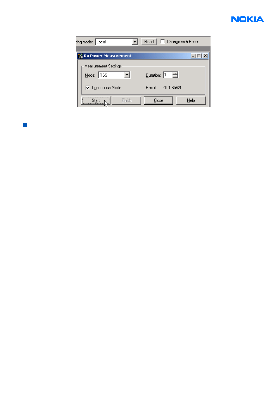
1. From the Testing menu in Phoenix, choose WCDMA -> Rx Power Measurement.
2. In the Rx Power Measurement window, choose the following settings:
• Mode: RSSI
• Continuous Mode
Page 1–12 Company Confidential Issue 1
Copyright ©2005 Nokia. All Rights Reserved.
Page 13
RM-84/99
RF Troubleshooting and Manual Tuning Guide Nokia Customer Care
3. To perform the measurement, click Start.
Transmitter troubleshooting
General instructions for Tx troubleshooting
Context
• Tx troubleshooting requires Tx operation.
• Do not transmit on frequencies that are in use!
• Transmitter can be controlled in the local mode for diagnostic purposes.
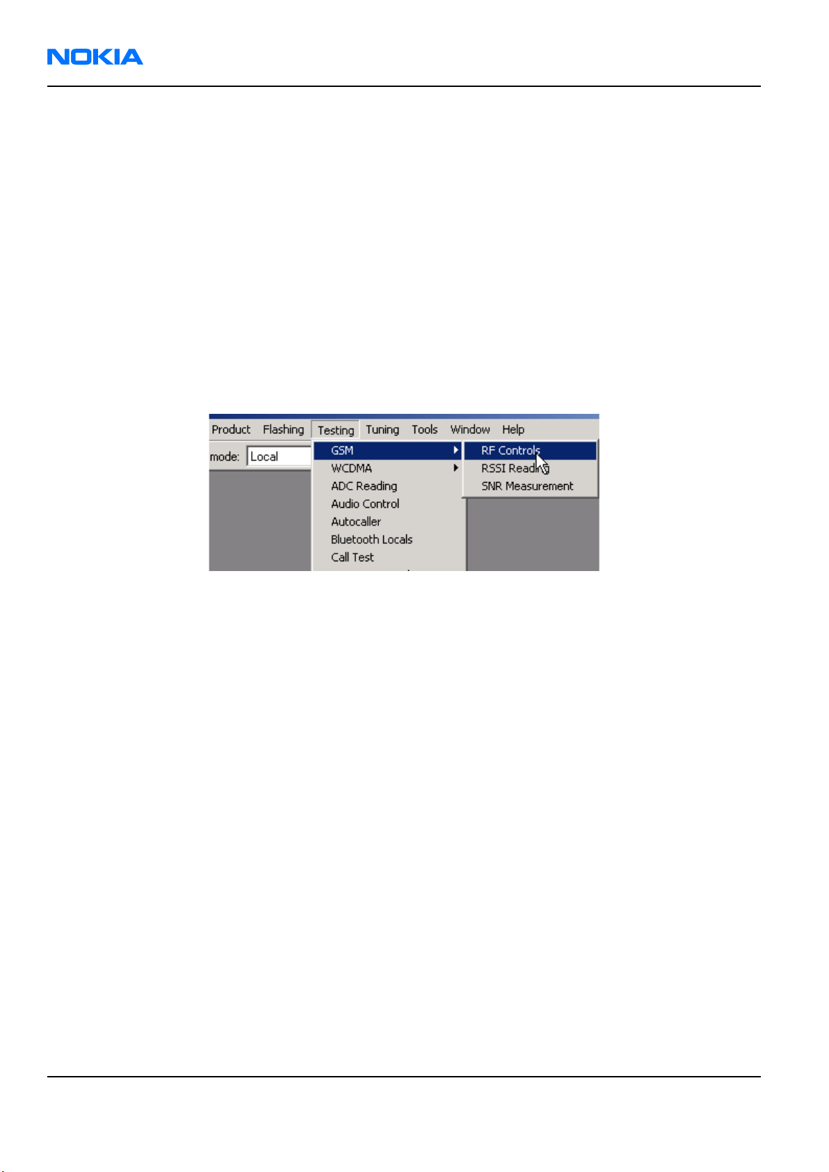
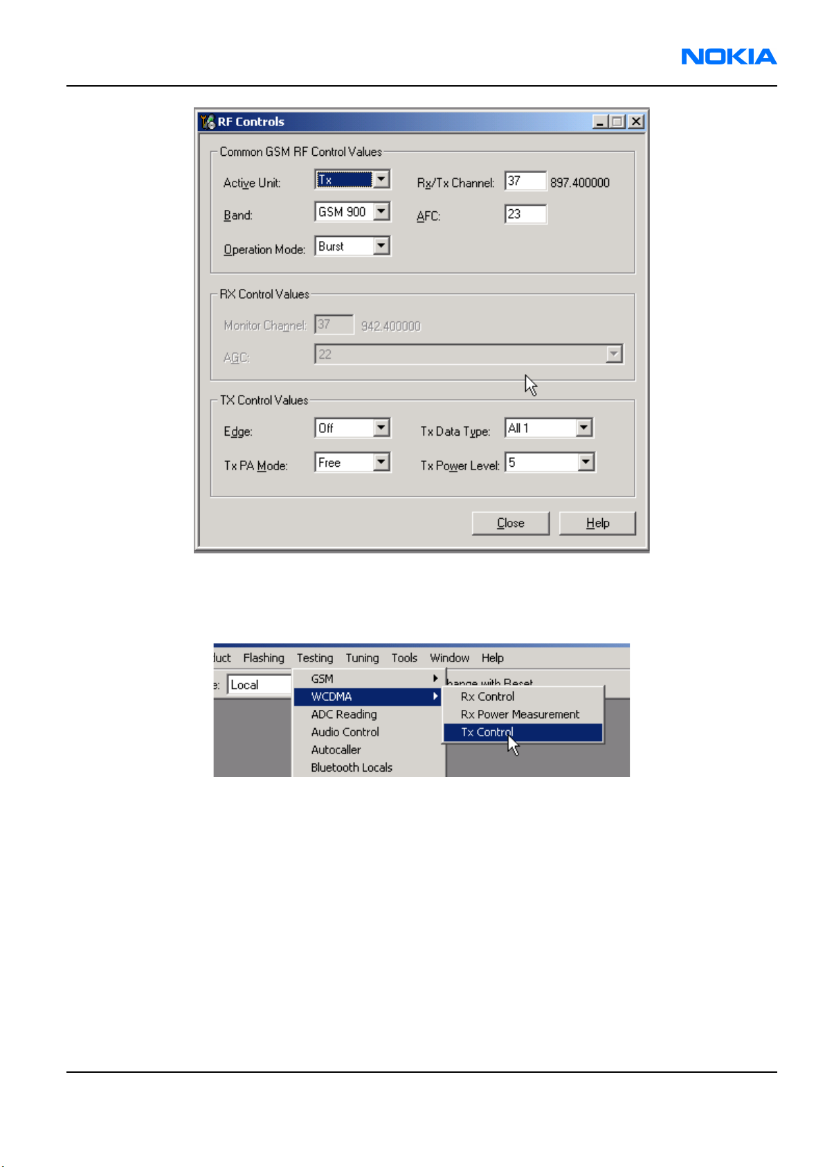
• The most useful Phoenix tool for GSM transmitter testing is "RF Controls"; in WCDMA transmitter testing the
best tool is "Tx Control".
• Tx IQ tuning and Tx power tuning can be also used in some cases.
• Remember that retuning is not a fix! Phones are tuned correctly in production.
The first set of steps instructs how to assemble the test setup. This setup is general for all Tx troubleshooting
tasks.
Alternative steps provide specific troubleshooting instructions for Phoenix service software. The first section is
for the EGSM900/GSM1800/GSM1900 bands and the latter for WCDMA.
Caution: Never activate the GSM or WCDMA transmitter without a proper antenna load. There should
be always 50 ohm load connected to the RF connector (antenna, RF-measurement equipment or at
least 2 watts dummy load), otherwise GSM or WCDMA PA may be damaged.
Steps
1. Connect a test jig to a computer with a DAU-9S cable or to a FPS-8 flash prommer with a modular cable.
Make sure that you have a PKD-1 dongle connected to the computer's parallel port.
2. Connect a DC power supply to a product-specific module jig.
Note: When repairing or tuning a transmitter, use an external DC supply with at least 3 A current
capability.
Set the DC supply voltage to 3.9 V and set the jumper connector on the test jig's reg.pass switch to
“ON” position.
3. Connect an RF cable between the RF connector of the product-specific module test jig and measurement
equipment or alternatively use a 50 ohms (at least 2 W) dummy load in the module test jig RF connector,
otherwise GSM or WCDMA PA may be damaged.
Note: There are three antenna connectors in the module jig:
• one for GSM
• one for WCDMA
• one for Bluetooth
Issue 1 Company Confidential Page 1–13
Copyright ©2005 Nokia. All Rights Reserved.
Page 14
RM-84/99
Nokia Customer Care RF Troubleshooting and Manual Tuning Guide
Make sure that all connections are made to the correct RF connector.
Normally a spectrum analyser is used as measurement equipment.
Note: The maximum input power of a spectrum analyser is +30 dBm.
To prevent any damage, it is recommended to use 10 dB attenuator on the spectrum analyzer input.
4. Set Tx on.
i Set the phone module to the test jig and start Phoenix service software.
ii Initialize connection to the phone. (With FPS-8 use FBUS driver when using DAU-9S and COMBOX driver).
iii From the File menu, choose product: File -> Choose Product -> xx-x* (* = type designator of the phone).
iv From the toolbar, set Operating mode to “Local”.
Alternative steps
• EGSM900/GSM1800/GSM1900 troubleshooting
i From the Testing menu, activate the RF Controls window: Testing -> GSM -> RF Controls .
ii In the RF Controls window:
• Select band “GSM900” or “GSM1800” or “GSM1900” (Default = “GSM900”).
• Set Active unit to “Tx” (Default = “Rx”).
• Set Operation mode to “Burst” (Default = “Burst”).
• Set Tx data type to “All1” (Default = “All1”).
• Set Rx/Tx channel to 37 on GSM900 band or 700 on GSM1800 band or 661 on GSM1900 (Defaults).
• Set Edge to “Off” (Default).
• Set Tx PA mode to “Free” (Default).
• Set power level to 5 (Default = 19) on GSM900 or to 0 (Default = 15) on GSM1800 or GSM1900.
Page 1–14 Company Confidential Issue 1
Copyright ©2005 Nokia. All Rights Reserved.
Page 15
RM-84/99
RF Troubleshooting and Manual Tuning Guide Nokia Customer Care
Figure 8 RF Controls window
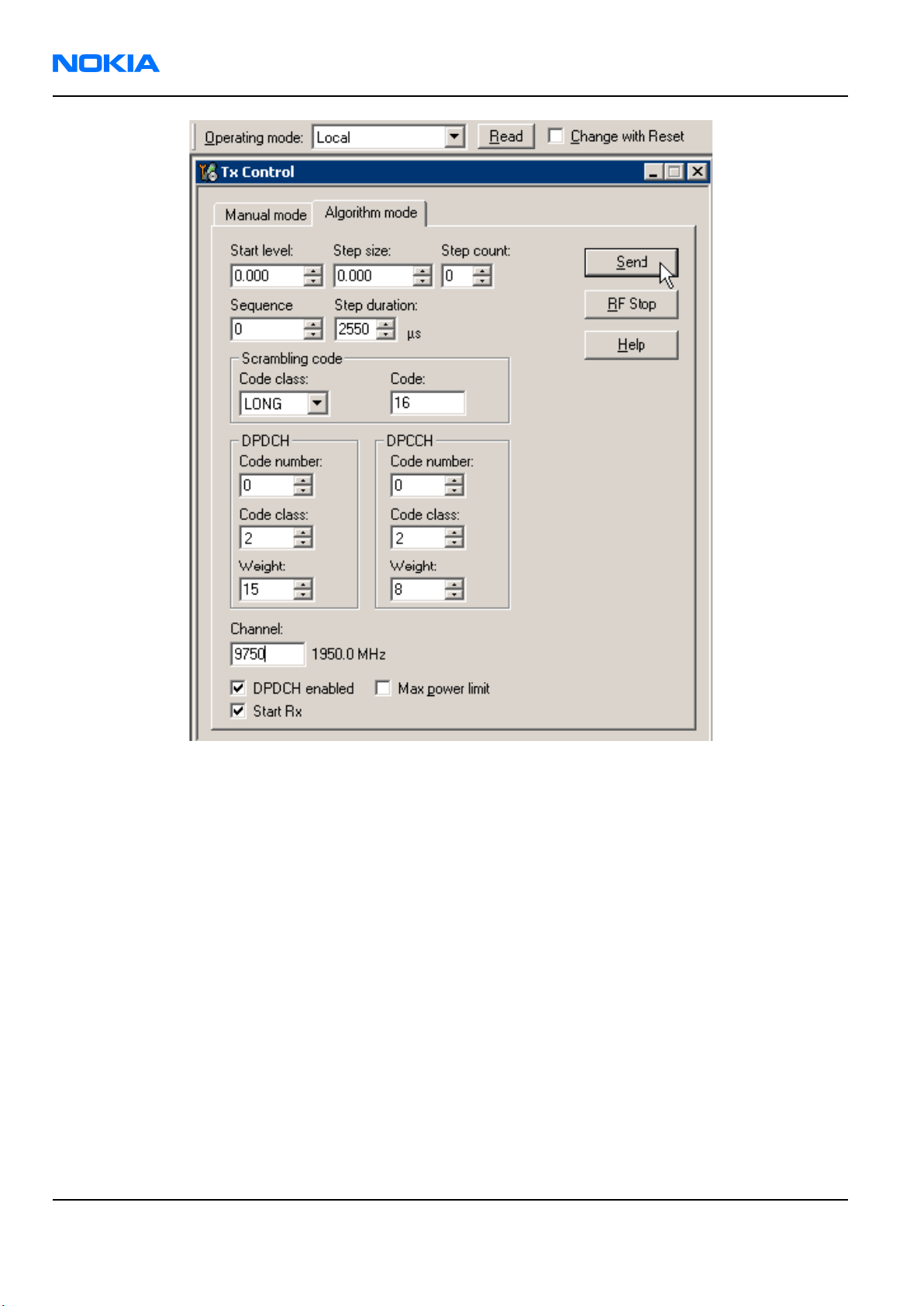
• WCDMA troubleshooting
i From the Testing menu, activate the Tx Control window:Testing -> WCDMA -> Tx Control .
ii In the Tx Control window:
• Select the Algorithm mode tab.
• Set Start level to “0” dBm (Default = “0”).
• Set Step size, Step count and Sequence to “0” (Default = “0”).
• Set Scrambling code class to “LONG” (Default = “LONG”).
• Set Scrambling code to “16” (Default = “16”).
• Set DPDCH Code number to “0”, Code class to “2” and Weight to “15” (Defaults).
• Set DPCCH Code number to “0”, Code class to "2" and Weight to “8” (Defaults).
• Set Channel to 9750.
• Check the "DPDCH enabled" checkbox (Default).
Issue 1 Company Confidential Page 1–15
Copyright ©2005 Nokia. All Rights Reserved.
Page 16
RM-84/99
Nokia Customer Care RF Troubleshooting and Manual Tuning Guide
Figure 9 Tx Control window
Next action
When settings are done, click “Send” to enable them.
If you change the settings (e.g. give a new channel number), you need to click “Stop” and “Send” again.
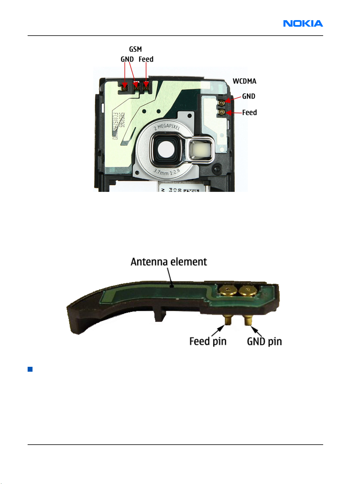
Checking antenna functionality
The main antenna has two separate antenna elements: GSM and WCDMA.
Note: RM-99 only has the GSM antenna element.
In the GSM antenna, there is one Feed and two GND contacts.
In the WCDMA antenna, there is one Feed and one GND contact.
The contacts of the GSM antenna are separated in the (RDC = 0 ohm) short-circuit. The contacts of the WCDMA
antenna are in the (RDC = 0 ohm) short-circuit.
Page 1–16 Company Confidential Issue 1
Copyright ©2005 Nokia. All Rights Reserved.
Page 17
RM-84/99
RF Troubleshooting and Manual Tuning Guide Nokia Customer Care
Figure 10 Feed and GND spots of the main antenna
The antenna is functioning normally when the contacts function (RDC = 0 ohm) and the antenna is visually intact.
BT antenna
BT antenna has one Feed and two GND contacts. The antenna is functioning normally when the contacts function
(RDC = 0 ohm) and the antenna is visually intact.
Figure 11 BT antenna
RF tunings
Introduction to RF tunings
Phone RF is tuned in production. There is no reason to do the re-calibration unless:
• One or more of the RF components is changed
• FLASH memory chip (D3000) is changed or otherwise corrupted.
Issue 1 Company Confidential Page 1–17
Copyright ©2005 Nokia. All Rights Reserved.
Page 18
RM-84/99
Nokia Customer Care RF Troubleshooting and Manual Tuning Guide
Note: RF calibration is always performed with the help of a product-specific module jig, never with
an RF coupler. Using an RF coupler in the calibration phase will cause a complete mistuning of the RF
side.
Important: After RF component changes, always use autotuning. Manual tunings are only required
in rare cases.
Cable and adapter losses
RF cables and adapters have some losses. They have to be taken into account when the phone is tuned. As all
the RF losses are frequency dependent, the user have to be very careful and understand the measurement setup.
The following table presents the RF attenuations of the product-specific module jig:
Band Attenuation
GSM900 0.3 dB
GSM1800 0.4 dB
GSM1900 0.5 dB
WCDMA 2100 0.8 dB
RF autotuning
RF autotuning
Before you begin
For information on the recommended test set-up, refer to the corresponding information on PWS/NOL.
Before you can use the auto-tune feature, the GPIB driver from the GPIB card vendor must be installed and
running.
The autotune .ini file must be in a correct place: C:\Program Files\Nokia\Phoenix\products\xx-x*
\autotune_xx-x*.ini (*= indicates the type designator of the phone, e.g. RM-1)
Context
RF autotuning is performed with the aid of Digital Radio Communication Tester. Autotuning covers all RF tunings
that are needed to perform after RF component repairs.
Note: Do not perform RF autotuning without a proper reason. Phones are tuned in production and an
RF tuning may be performed only after component repairs or if the RF tuning information is lost.
Steps
1. Connect the communication tester to the GPIB bus.
2. Start Phoenix service software.
Page 1–18 Company Confidential Issue 1
Copyright ©2005 Nokia. All Rights Reserved.
Page 19
RM-84/99
RF Troubleshooting and Manual Tuning Guide Nokia Customer Care
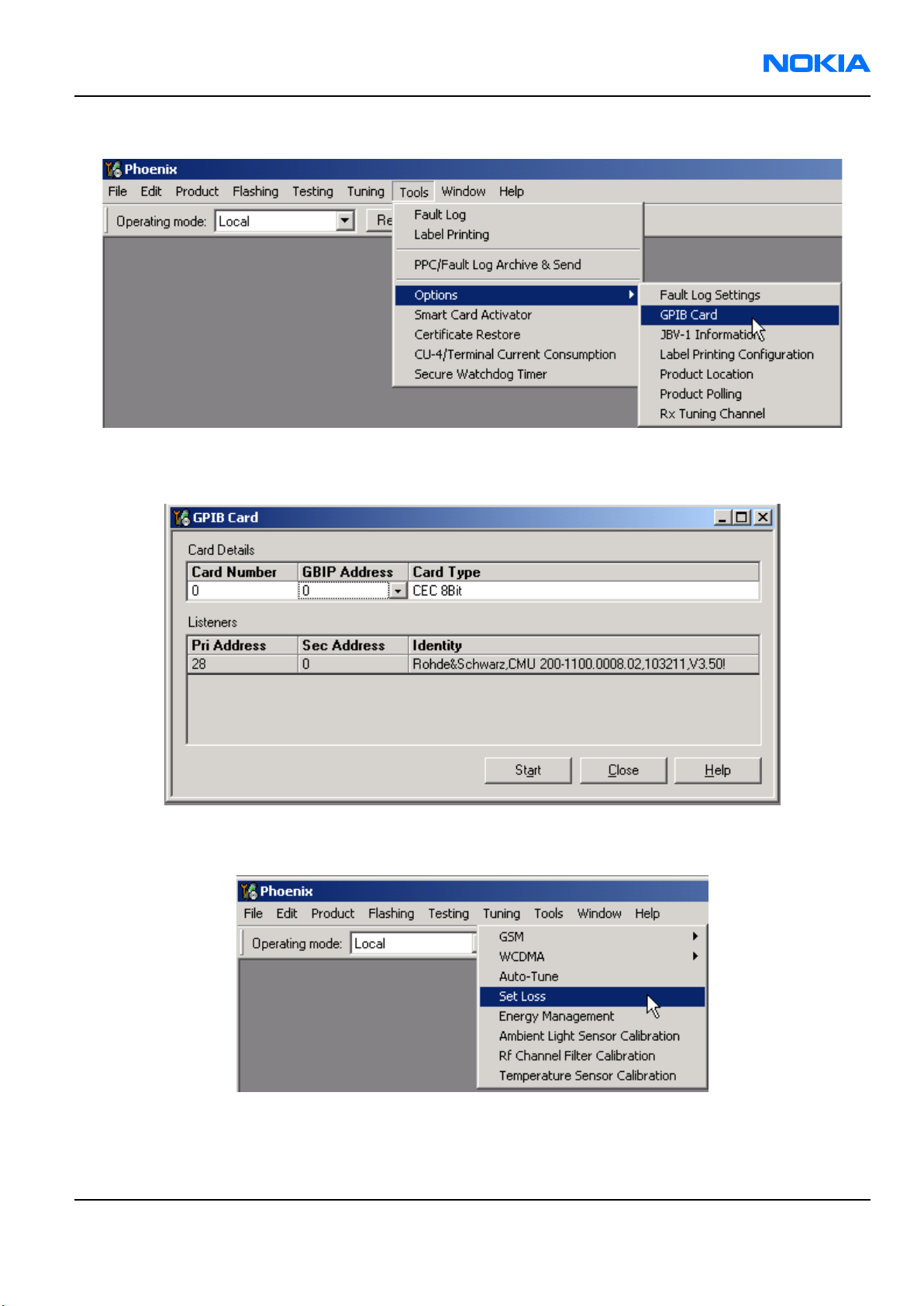
3. From the Tools menu, choose Options -> GPIB Card.
4. In the Card Type line, select CEC8Bit, then click Start.
After clicking Start, the name of the communication tester appears in the list of found Listeners.
5. To specify the cable loss from module jig to the communication tester, choose "Set Loss" from the Tuning
menu.
Issue 1 Company Confidential Page 1–19
Copyright ©2005 Nokia. All Rights Reserved.
Page 20
RM-84/99
Nokia Customer Care RF Troubleshooting and Manual Tuning Guide
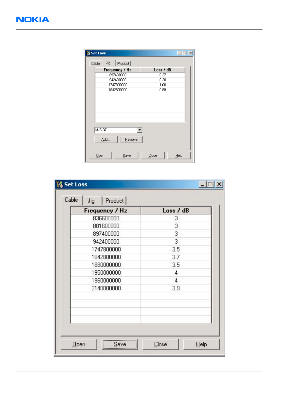
6. In the Set Loss window, click the Jig tab and select the right jig for the phone.
7. Click the Cable tab and add the extra cable attenuation.
Page 1–20 Company Confidential Issue 1
Copyright ©2005 Nokia. All Rights Reserved.
Page 21

RM-84/99
RF Troubleshooting and Manual Tuning Guide Nokia Customer Care
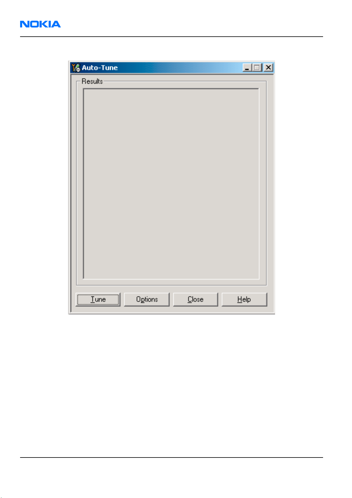
8. To start autotuning, choose Auto-Tune from the Tuning menu.
9. In the Auto-Tune window, click Options.
10. In the Auto-Tune options window, see that the "Enable showing of messages" check box is checked, then
click OK.
Issue 1 Company Confidential Page 1–21
Copyright ©2005 Nokia. All Rights Reserved.
Page 22
RM-84/99
Nokia Customer Care RF Troubleshooting and Manual Tuning Guide
11. Connect the phone's WCDMA RF port to the communication tester, and click Tune.
Page 1–22 Company Confidential Issue 1
Copyright ©2005 Nokia. All Rights Reserved.
Page 23
RM-84/99
RF Troubleshooting and Manual Tuning Guide Nokia Customer Care
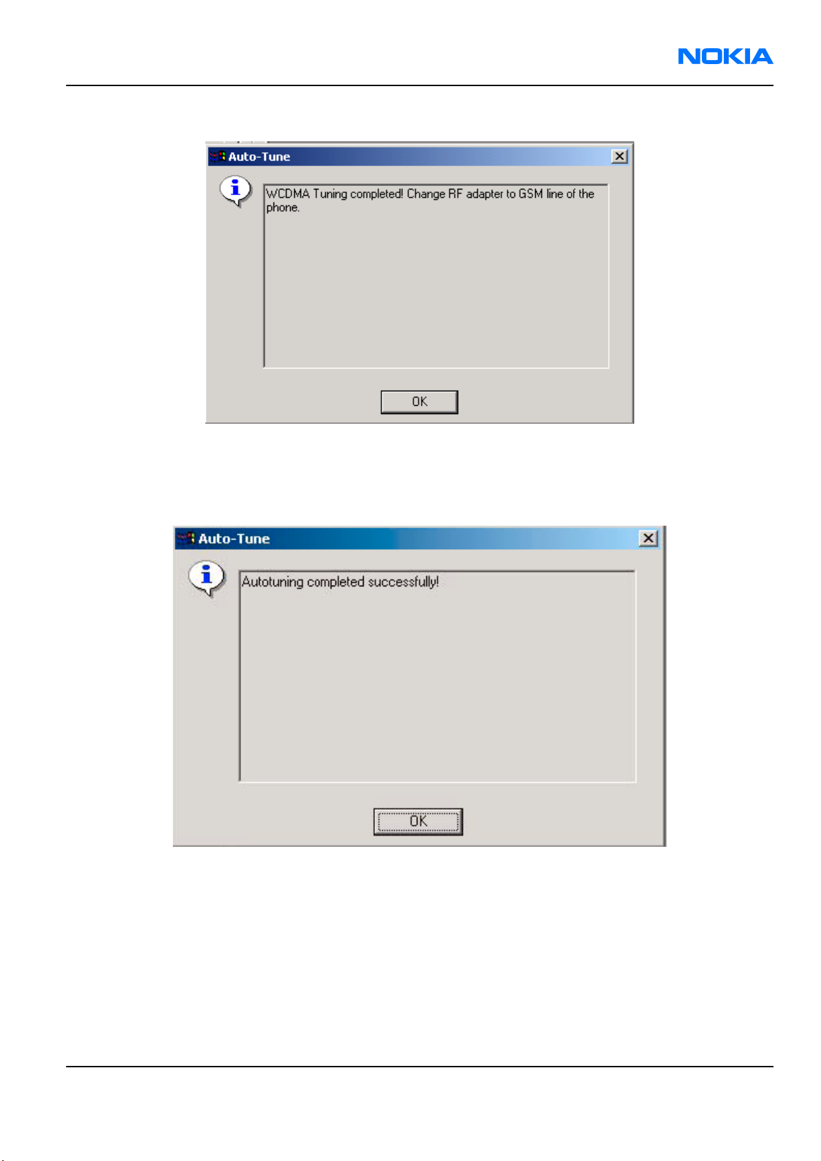
12. Change the phone's RF adapter from WCDMA port to GSM port.
13. To complete the RF autotuning, click OK.
Results
"Autotuning completed successfully" message appears.
RF manual tuning guide
Required manual tunings after component changes
Important: After RF component changes, always use autotuning. Manual tunings are only required
in rare cases.
If, however, manual tuning is used, only relevant tunings should be performed. Refer to the following table:
Issue 1 Company Confidential Page 1–23
Copyright ©2005 Nokia. All Rights Reserved.
Page 24
RM-84/99
Nokia Customer Care RF Troubleshooting and Manual Tuning Guide
Changed component Perform the following tunings
Tx RF ASIC Vinku (N7501) RF Channel Filter Calibration, Tx IQ Tuning, Tx Power
Level Tuning, Temperature Sensor Calibration, TX AGC
& Power Detector, Tx Band Response Calibration, Tx
LO Leakage
RX RF ASIC Hinku (N7500) RF Channel Filter Calibration, Rx Calibration, Rx Band
Filter Response Compensation, Rx AM Suppression, Rx
AGC Alignment, Rx Band Response Calibration
Any component in the GSM TX RF chain before the PA Tx IQ Tuning, Tx Power Level Tuning
Any component in the GSM TX RF chain after the PA
or PA
Any component in the WCDMA TX RF chain before thePATx AGC & Power Detector, Tx Band Response
Any component in the WCDMA TX RX chain after the
PA, PA, power detector or PA switch mode power
supply
Any component in the GSM RX chain Rx Calibration, RX Band Filter Response
Any component in the WCDMA RX chain Rx AGC Alignment, RX Band Response Calibration
VCTCXO (G7501) Rx Calibration (GSM900 band)
Tx Power Level Tuning
Calibration, Tx LO Leakage
Tx AGC & Power Detector, Tx Band Response
Calibration, PA Detection
Compensation, RX AM Suppression
System mode independent manual tunings
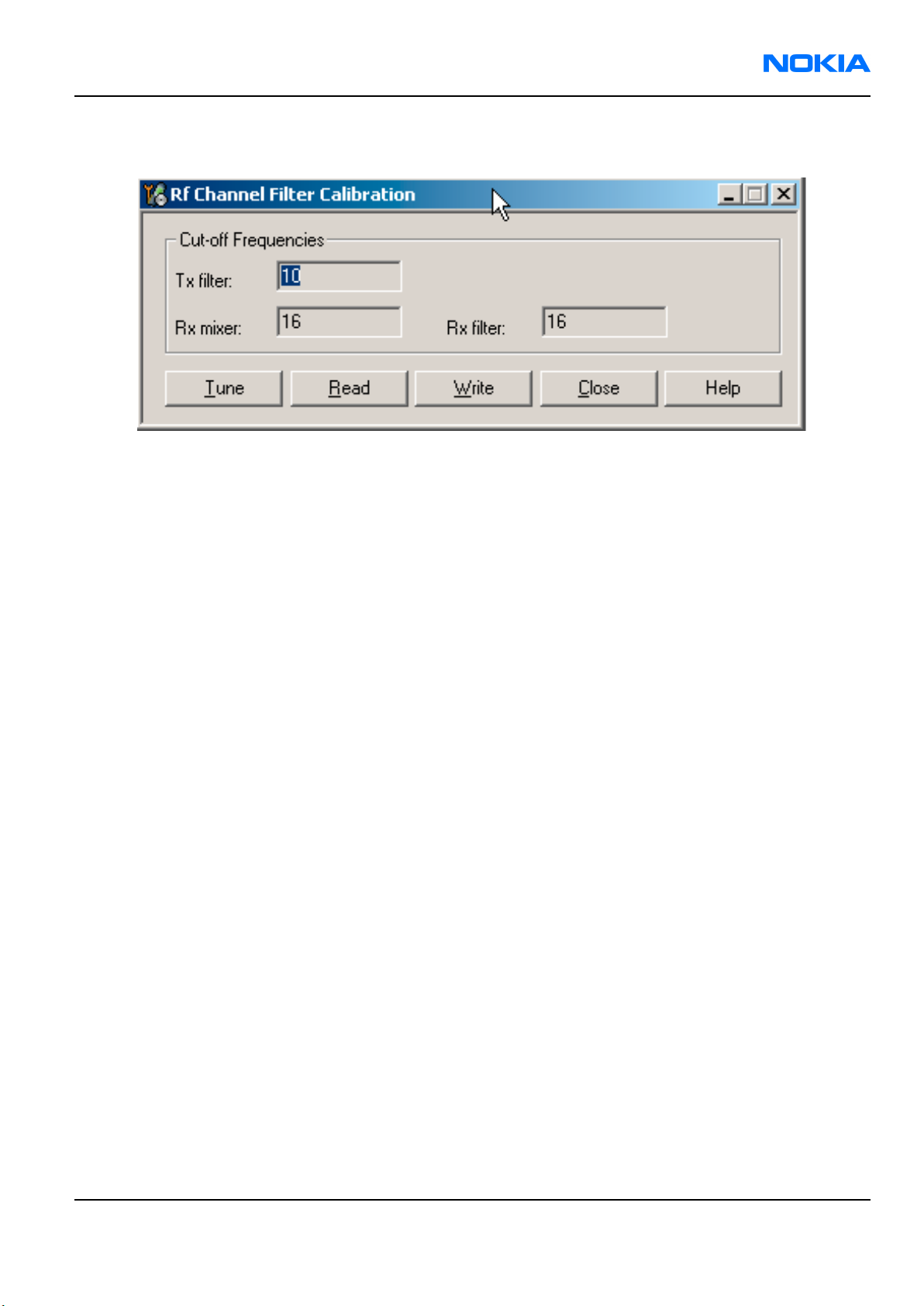
RF channel filter calibration
Context
Rx channel filter calibration tunes Rx and Tx ASICs' internal low pass filters that limit the bandwidth of BB IQ
signals.
One common calibration is made for GSM and WCDMA.
Table 1 RF channel filter calibration tuning limits
Min Typ Max
Tx filter 0 10 31
Rx filter 0 16 31
Steps
1. From the "Operating mode" dropdown menu, set mode to "Local".
2. From the Tuning menu, choose "RF Channel Filter Calibration".
3. Click Tune.
4. To save the values to the PMM (Permanent Memory) area, click Write.
5. To close the tuning window, click Close.
Page 1–24 Company Confidential Issue 1
Copyright ©2005 Nokia. All Rights Reserved.
Page 25
RM-84/99
RF Troubleshooting and Manual Tuning Guide Nokia Customer Care
Results
Figure 12 RF channel filter calibration typical values
PA (power amplifier) detection
Context
PA detection procedure detects which PA manufacturer is used for GSM and WCDMA PAs.
If PA is changed or if the permanent memory (PMM) data is corrupted, PA detection has to be performed before
Tx tunings.
Steps
1. From the "Operating mode" dropdown menu, set mode to "Local".
2. From the Tuning menu, choose "PA Detection".
3. Click Tune.
4. Check that the detected PA manufacturers are corresponding to the actual chips on the board.
5. To end the procedure, click Close.
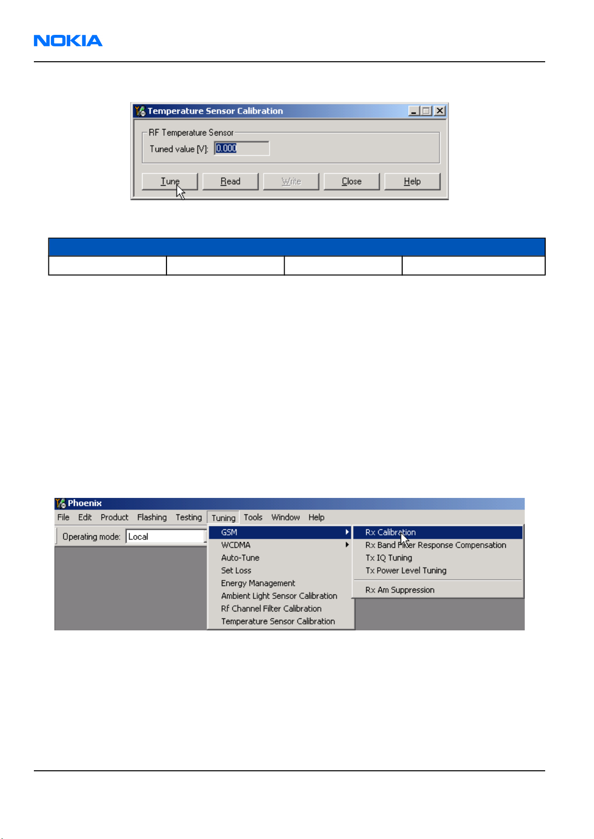
Temperature sensor calibration
Context
There is a temperature sensor integrated into VINKU ASIC. VINKU provides DC-voltage, which is temperature
dependent.
Temperature sensor calibration is done in room temperature, in which offset caused by VINKU variation and
AD-converter inside RETU are nullified.
The module is able to do this calibration by itself, no external equipment is needed.
The temperature of the module and components must be 23 +/-2 degrees.
Steps
1. From the "Operating mode" dropdown menu, set mode to "Local".
2. From the Tuning menu, choose "Temperature Sensor Calibration".
Issue 1 Company Confidential Page 1–25
Copyright ©2005 Nokia. All Rights Reserved.
Page 26
RM-84/99
Nokia Customer Care RF Troubleshooting and Manual Tuning Guide
3. Click "Tune".
Table 2 Temperature sensor calibration tuning limits
Min Typ Max Unit
-20 -4 20 V
4. To save the calibration values, click "Write".
5. To finish the calibration, click "Close".
GSM receiver tunings
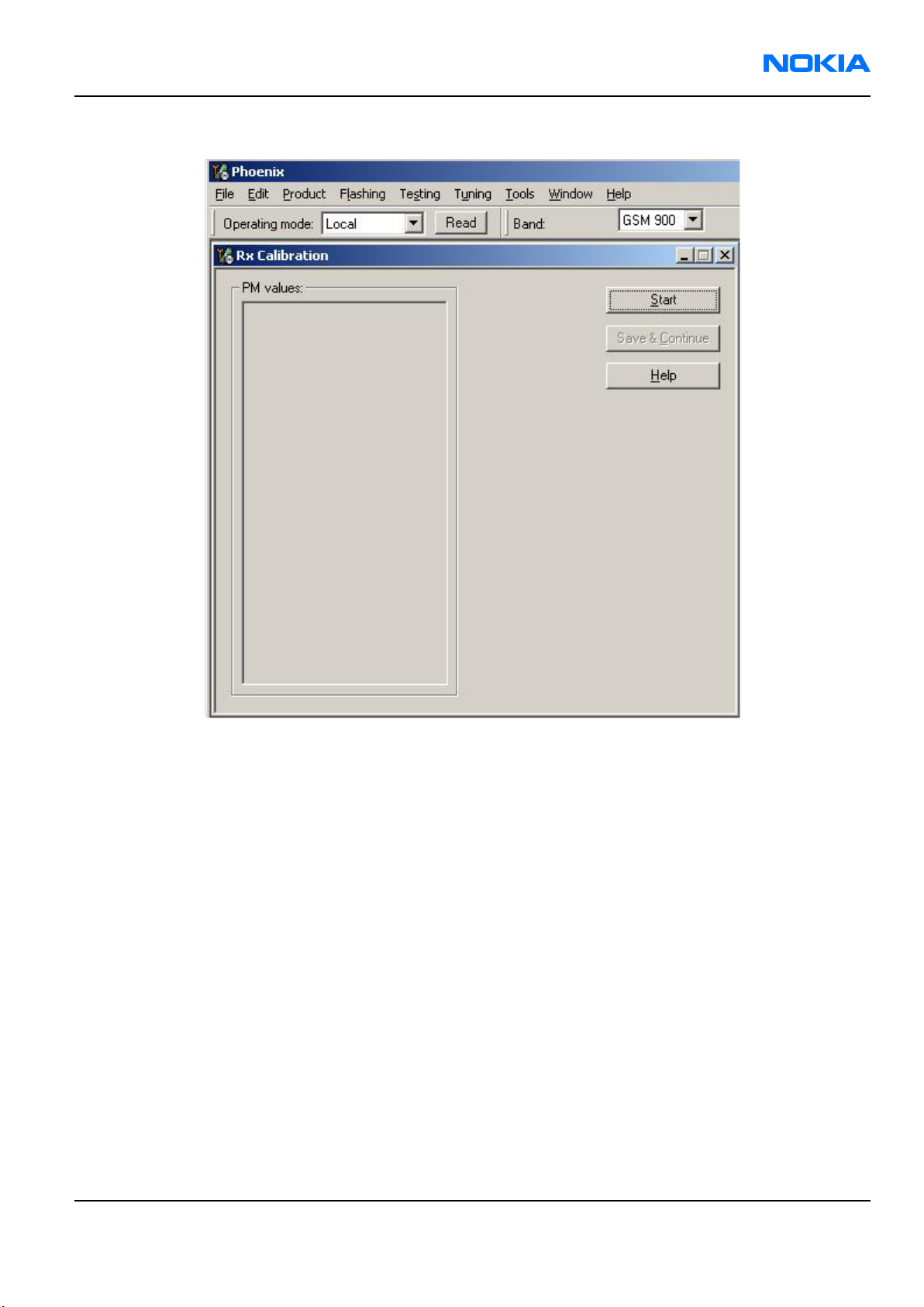
Rx calibration (GSM)
Context
Rx Calibration is used to find out the real gain values of the GSM Rx AGC system and tuning response of the AFC
system (AFC D/A init value and AFC slope)
Steps
1. Connect the module jig’s GSM connector to signal generator.
2. From the "Operating mode" dropdown menu, set mode to "Local".
3. From the Tuning menu, choose GSM -> Rx Calibration.
4. Check the “Load from Phone” check box and clear the “Save to Phone” check box.
5. From the Band dropdown menu, choose GSM900.
Page 1–26 Company Confidential Issue 1
Copyright ©2005 Nokia. All Rights Reserved.
Page 27
RM-84/99
RF Troubleshooting and Manual Tuning Guide Nokia Customer Care
6. Click Start (if not active already).
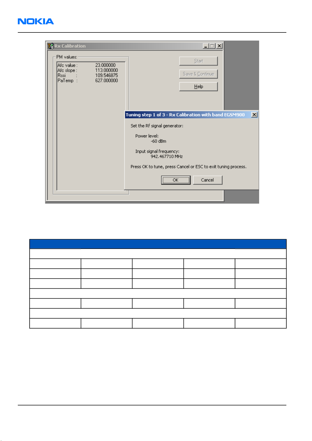
7. Click Calibrate.
8. Connect signal generator to the phone and set frequency and amplitude as instructed in the "Rx Calibration
with band EGSM900" popup window.
The calibration uses a non-modulated CW signal. Increase the signal generator level by cable attenuation
and module jig probe attenuation!
Issue 1 Company Confidential Page 1–27
Copyright ©2005 Nokia. All Rights Reserved.
Page 28
RM-84/99
Nokia Customer Care RF Troubleshooting and Manual Tuning Guide
9. To perform tuning, click OK.
10. Check that the tuning values are within the limits specified in this table:
Table 3 RF tuning limits in Rx calibration
Min Typ Max Unit
GSM900
AFC Value -200 -105...62 200
AFC slope 0 122 200
RSSI0 106 107...110 114 dB
GSM1800
RSSI0 104 104...109 114 dB
GSM1900
RSSI0 104 104...109 114 dB
Page 1–28 Company Confidential Issue 1
Copyright ©2005 Nokia. All Rights Reserved.
Page 29
RM-84/99
RF Troubleshooting and Manual Tuning Guide Nokia Customer Care
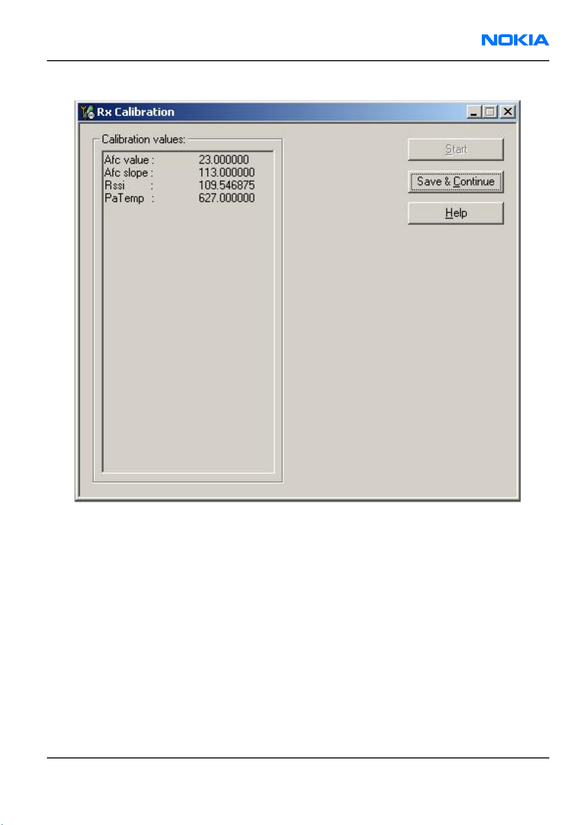
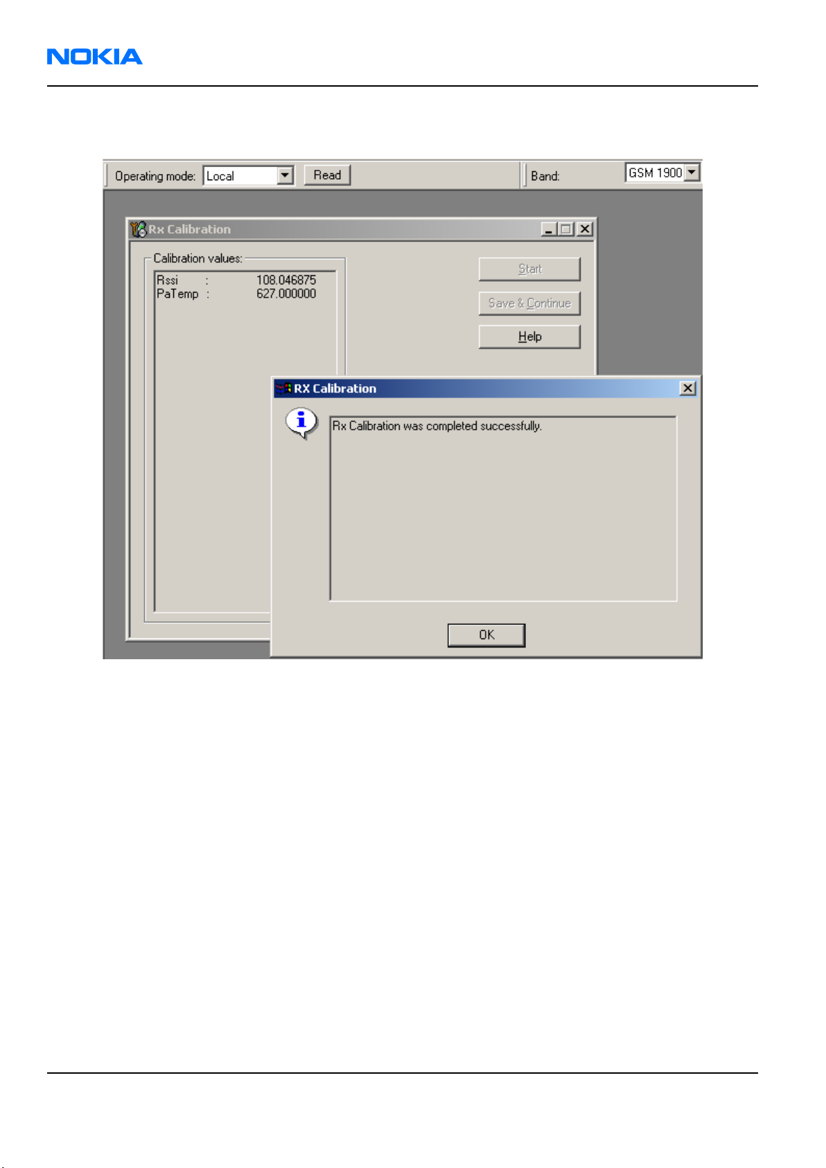
11. To save values to the phone, click "Save & Continue".
12. Repeat steps 3 to 8 for GSM1800 and GSM1900.
Issue 1 Company Confidential Page 1–29
Copyright ©2005 Nokia. All Rights Reserved.
Page 30
RM-84/99
Nokia Customer Care RF Troubleshooting and Manual Tuning Guide
Results
Rx band filter response compensation (GSM)
Before you begin
Rx Calibration must be performed before the Rx Band Filter Response Compensation.
Context
On each GSM Rx band, there is a band rejecting filter in front of the HINKU front end. The amplitude ripple caused
by these filters causes ripple to the RSSI measurement and therefore calibration is needed.
The calibration has to be repeated for each GSM band.
Steps
1. Connect the module jig’s GSM connector to the signal generator.
2. From the "Operating mode" dropdown menu, set mode to "Local".
3. Select GSM900 band.
Page 1–30 Company Confidential Issue 1
Copyright ©2005 Nokia. All Rights Reserved.
Page 31

RM-84/99
RF Troubleshooting and Manual Tuning Guide Nokia Customer Care
4. From the Tuning menu, choose GSM -> Rx Band Filter Response Compensation.
5. In the Tuning mode pane, select Manual.
6. Click Start.
Issue 1 Company Confidential Page 1–31
Copyright ©2005 Nokia. All Rights Reserved.
Page 32

RM-84/99
Nokia Customer Care RF Troubleshooting and Manual Tuning Guide
7. Click Save & Continue.
Page 1–32 Company Confidential Issue 1
Copyright ©2005 Nokia. All Rights Reserved.
Page 33

RM-84/99
RF Troubleshooting and Manual Tuning Guide Nokia Customer Care
8. Connect the signal generator to the phone and set frequency and amplitude as instructed in the "Rx Band
Filter Response Compensation for EGSM900" popup window.
9. To perform tuning, click OK.
10. Go through all 9 frequencies.
11. Check that the tuning values are within the limits specified in the following table:
Min Typ Max Unit
GSM900
Ch. 965 /
923.26771 MHz
Ch. 975 /
925.26771 MHz
Ch. 987 /
927.66771 MHz
Ch. 1009 /
932.06771 MHz
Ch. 37 / 942.46771
MHz
Issue 1 Company Confidential Page 1–33
-10 -1 5 dB
-3 0 5 dB
-3 0 5 dB
-3 0 5 dB
-3 0 5 dB
Copyright ©2005 Nokia. All Rights Reserved.
Page 34

RM-84/99
Nokia Customer Care RF Troubleshooting and Manual Tuning Guide
Min Typ Max Unit
Ch. 90 / 953.06771
MHz
Ch. 114 /
957.86771 MHz
Ch. 124 /
959.86771 MHz
Ch. 136 /
962.26771 MHz
GSM1800
Ch. 497 /
1802.26771 MHz
Ch. 512 /
1805.26771 MHz
Ch. 535 /
1809.86771 MHz
Ch. 606 /
1824.06771 MHz
Ch. 700 /
1842.86771 MHz
-3 0 5 dB
-3 0 5 dB
-3 0 5 dB
-10 -1 5 dB
-10 -1 5 dB
-3 0 5 dB
-3 0 5 dB
-3 0 5 dB
-3 0 5 dB
Ch. 791 /
1861.06771 MHz
Ch. 870 /
1876.86771 MHz
Ch. 885 /
1879.86771 MHz
Ch. 908 /
1884.46771 MHz
GSM1900
Ch. 496 /
1927.06771 MHz
Ch. 512 /
1930.26771 MHz
Ch. 537 /
1935.26771 MHz
Ch. 586 /
1945.06771 MHz
Ch. 661 /
1960.06771 MHz
-3 0 5 dB
-3 0 5 dB
-3 0 5 dB
-10 -1 5 dB
-10 -1 5 dB
-3 0 5 dB
-3 0 5 dB
-3 0 5 dB
-3 0 5 dB
Ch. 736 /
1975.06771 MHz
Page 1–34 Company Confidential Issue 1
-3 0 5 dB
Copyright ©2005 Nokia. All Rights Reserved.
Page 35

RM-84/99
RF Troubleshooting and Manual Tuning Guide Nokia Customer Care
Min Typ Max Unit
Ch. 794 /
1986.66771 MHz
Ch. 810 /
1989.86771 MHz
Ch. 835 /
1994.86771 MHz
12. If the values are within the limits, click "Save & Continue".
-3 0 5 dB
-3 0 5 dB
-10 -1 5 dB
13. Repeat the steps 4 to 10 for GSM1800 and GSM1900.
Issue 1 Company Confidential Page 1–35
Copyright ©2005 Nokia. All Rights Reserved.
Page 36

RM-84/99
Nokia Customer Care RF Troubleshooting and Manual Tuning Guide
Results
Rx AM suppression (GSM)
Context
Rx AM suppression is used to tune the AM suppression capabilities of the GSM receiver.
AM suppression is related to ability of the receiver to operate when there is a disturbing AM modulated signal
near the received channel signal frequency.
RFIC has tunable compensation circuit which has an effect on the AM suppression ability.
In Rx AM suppression, a continuous useful signal accompanied with an AM modulated signal 10MHz above the
current channel is fed to the antenna. RFIC control word values are iterated until a minimum RSSI signal is found.
Steps
1. Connect the module jig’s GSM connector to the signal generator.
2. From the "Operating mode" dropdown menu, set mode to "Local".
3. From the Tuning menu, choose GSM -> Rx AM Suppression.
Page 1–36 Company Confidential Issue 1
Copyright ©2005 Nokia. All Rights Reserved.
Page 37

RM-84/99
RF Troubleshooting and Manual Tuning Guide Nokia Customer Care
4. Select GSM900 band.
5. Click Start.
6. Connect the signal generator to the phone according to the frequency and modulation parameters
displayed in the pop-up window:
Frequency 952.46771MHz / 1852.86771MHz / 1970.06771
MHz (depending on the band used)
Power level -25 dBm / -26 dBm / -29 dBm (increase by cable
and jig attenuations)
Modulation AM
AM modulation depth 90%
Modulation signal 50 kHz sinewave (or 15 kHz if 50 kHz is not
available)
Issue 1 Company Confidential Page 1–37
Copyright ©2005 Nokia. All Rights Reserved.
Page 38

RM-84/99
Nokia Customer Care RF Troubleshooting and Manual Tuning Guide
7. Click OK.
8. Check that RSSI level value is between the limits presented in the following table.
Table 4 RSSI level values
Band Min Max Unit
GSM900 -115 -90 dB
GSM1800 -115 -85 dB
GSM1900 -115 -100 dB
9. To proceed to the next band, click "Next".
Page 1–38 Company Confidential Issue 1
Copyright ©2005 Nokia. All Rights Reserved.
Page 39

RM-84/99
RF Troubleshooting and Manual Tuning Guide Nokia Customer Care
10. To end the tuning, click "Finish" and "Close".
GSM transmitter tunings
Tx IQ tuning (GSM)
Context
• The Tx path branches to I and Q signals at RF I/Q modulator. Modulator and analog hardware located after
it cause unequal amplitude and phase disturbance to I and Q signal paths. Tx IQ tuning balances the I and Q
branches.
• Tx IQ tuning must be performed on all GSM bands.
Steps
1. From the dropdown menus, set "Operating mode" to Local, "System mode" to GSM, and "Band" to GSM900.
Issue 1 Company Confidential Page 1–39
Copyright ©2005 Nokia. All Rights Reserved.
Page 40

RM-84/99
Nokia Customer Care RF Troubleshooting and Manual Tuning Guide
2. From the Tuning menu, choose GSM -> Tx IQ Tuning.
3. Set "Mode" to Automatic and "Edge" to Off.
4. Click Start.
Wait until automatic tuning has finished and moved the sliders.
Values are written to the phone memory automatically.
Page 1–40 Company Confidential Issue 1
Copyright ©2005 Nokia. All Rights Reserved.
Page 41

RM-84/99
RF Troubleshooting and Manual Tuning Guide Nokia Customer Care
5. When the values have been written to the phone memory, click Next to change to the next band.
6. When all bands have been tuned, click Finish and Close to end the tuning procedure.
Next action
Tuning sliders should be close to the center of the scale after the tuning and within the limits specified in the
following table. If they are not within the limits, check Tx IQ quality manually.
Min Typ Max Unit
GSM900
I DC offset / Q DC
offset
Ampl -1 0 1 dB
Phase 85 90 95 dB
GSM1800/GSM1900
I/Q DC -6 0.5 6 dB
Ampl -1 0 1 dB
Phase 95 100 110 dB
Issue 1 Company Confidential Page 1–41
-6 -4 4 6 dB
Copyright ©2005 Nokia. All Rights Reserved.
Page 42

RM-84/99
Nokia Customer Care RF Troubleshooting and Manual Tuning Guide
Tx power level tuning (GSM)
Context
Because of variations at IC process and discrete component values, the actual transmitter RF gain of each phone
is different. Tx power level tuning is used to find out mapping factors called 'power coefficients’. These adjust
the GSM transmitter output power to fulfill the specifications.
In dual or triple band phones, the power level tuning is made for both high and low PA Modes (Power Amplifier
Mode) in the GSM900 band but only for high PA mode in GSM1800/GSM1900 bands
For EDGE transmission the bias settings of the GSM PA are adjusted in order to improve linearity. This affects
the PA gain and hence the power levels have to be aligned separately for EDGE transmission.
Tx power level tuning has to be performed on all GSM bands.
Steps
1. Connect the phone to a spectrum analyzer.
2. Start Phoenix service software.
3. From the "Operating mode" dropdown menu, set mode to "Local".
4. From the Tuning menu, choose GSM -> Tx Power Level Tuning.
5. Set the spectrum analyzer for power level tuning:
Frequency channel frequency (897.4MHz GSM900, 1747.8MHz
GSM1800, 1880MHz GSM1900)
Span 200 kHz
Sweep time 3s
Trigger Video triggering: Free run
Resolution BW 3 kHz
Video BW 3 kHz
Reference level offset sum cable attenuation with module jig
attenuation
Reference level 33dBm
A power meter with a peak power detector can be also used. Remember to take the attenuations in the
account!
Page 1–42 Company Confidential Issue 1
Copyright ©2005 Nokia. All Rights Reserved.
Page 43

RM-84/99
RF Troubleshooting and Manual Tuning Guide Nokia Customer Care
6. Click Start.
Issue 1 Company Confidential Page 1–43
Copyright ©2005 Nokia. All Rights Reserved.
Page 44

RM-84/99
Nokia Customer Care RF Troubleshooting and Manual Tuning Guide
7. Adjust power levels 5, 15 and 19 to correspond the "Target dBm" column by pressing + or – keys.
Check that the coeffiecient values are within the limits specified in the following table.
Min Typ Max
GSM900 EDGE off
PL5 coefficient 0.45 0.626 0.73
PL15 coefficient 0.234
PL19 coefficient 0.12 0.195 0.3
GSM900 EDGE on
PL8 coefficient 0.35 0.419 0.6
PL15 coefficient 0.247
PL19 coefficient 0.12 0.204 0.3
GSM1800 EDGE off
PL0 coefficient 0.45 0.51 0.7
PL11 coefficient 0.219
PL15 coefficient 0.12 0.185 0.3
GSM1800 EDGE on
PL2 coefficient 0.35 0.394 0.6
Page 1–44 Company Confidential Issue 1
Copyright ©2005 Nokia. All Rights Reserved.
Page 45

RM-84/99
RF Troubleshooting and Manual Tuning Guide Nokia Customer Care
Min Typ Max
PL11 coefficient 0.23
PL15 coefficient 0.12 0.194 0.3
GSM1900 EDGE off
PL0 coefficient 0.45 0.482 0.7
PL11 coefficient 0.218
PL15 coefficient 0.12 0.184 0.3
GSM1900 EDGE on
PL2 coefficient 0.35 0.377 0.6
PL11 coefficient 0.23
PL15 coefficient 0.12 0.193 0.3
8. If the values are within the limits, click "Save & Continue" to proceed to the next band and click Start.
9. Set Edge mode on and start tuning again. Change video averaging to 50.
10. Tune EDGE power levels to the corresponding target power levels.
Only power levels 8, 15 and 19 are tuned in GSM900 and 2, 10 and 15 in GSM1800/1900.
11. When the tuning is completed, close the Tx Power Level Tuning window.
RM-84 WCDMA receiver tunings
Rx AGC alignment (WCDMA)
Context
Rx AGC alignment tuning is used to find out the real gain values of the WCDMA Rx AGC system and converters.
Steps
1. From the "Operating mode" dropdown menu, set mode to "Local".
2. From the Tuning menu, choose WCDMA -> Rx AGC Alignment.
Issue 1 Company Confidential Page 1–45
Copyright ©2005 Nokia. All Rights Reserved.
Page 46

RM-84/99
Nokia Customer Care RF Troubleshooting and Manual Tuning Guide
3. Click Start and Tune.
4. Setup the signal generator to correspond the values in the "RX AGC Calibration" pop-up window and click OK:
Frequency: 2141MHz
Level: –51 dBm + cable and adapter attenuations
Modulation: FM
Deviation: 500 kHz
Modulation frequency: 50 kHz
5. Check that the “Rx Chain” value in “Tuning Results” is within the limits presented in the following table.
Min Typ Max Unit
RX chain -6 1.5 3.5 6 dB
Low freq -5 -0.7 4.0 5
Page 1–46 Company Confidential Issue 1
Copyright ©2005 Nokia. All Rights Reserved.
Page 47

RM-84/99
RF Troubleshooting and Manual Tuning Guide Nokia Customer Care
Min Typ Max Unit
High freq -5 -0.7 4.0 5
i If the Rx gain is acceptable, click Yes to save the results to the phone.
6. To close the tuning window, click Close.
Rx band response calibration (WCDMA)
Context
There is a band rejecting filter for each WCDMA Rx band between the front end LNA and the mixer of HINKU. The
amplitude ripple caused by this filter causes ripple to the RSSI measurement and therefore Rx band response
calibration is needed.
Rx band response calibration can be done in two different ways. If the signal generator in use supports frequency
sweep table, the calibration can be done as a part of Rx calibration. If not, it is possible to calibrate all the
necessary frequencies one by one.
The first set of steps shows how to perform the calibration without the signal generator sweep feature and the
alternative steps give instructions how to perform the calibration if the signal generator supports frequency
sweeps and the calibration can be performed within Rx AGC calibration.
Steps
1. From the "Operating mode" dropdown menu, set mode to "Local".
2. From the Tuning menu choose WCDMA -> Rx Band Response Calibration.
Issue 1 Company Confidential Page 1–47
Copyright ©2005 Nokia. All Rights Reserved.
Page 48

RM-84/99
Nokia Customer Care RF Troubleshooting and Manual Tuning Guide
3. Click Start and Tune.
4. Setup the signal generator to correspond the values in the pop-up window:
Frequency: 2113.4MHz
Level: –48 dBm + cable and adapter attenuations
Modulation: FM
Deviation: 500 kHz
Modulation frequency: 50 kHz
5. Click OK.
6. Change frequency to 2166.6 MHz and click OK.
7. Check that the tuned values are within the limits specified in the table below:
Min Max
Frequency compensation low -5 +5
Frequency compensation high -5 +5
Page 1–48 Company Confidential Issue 1
Copyright ©2005 Nokia. All Rights Reserved.
Page 49

RM-84/99
RF Troubleshooting and Manual Tuning Guide Nokia Customer Care
i If the values are OK, click Yes to save the values.
8. Close the tuning window.
Alternative steps
• From the "Operating mode" dropdown menu, set mode to "Local".
• From the Tuning menu, choose WCDMA -> Rx AGC Alignment.
• Click Start.
• Check the “Tune Rx Band Response” checkbox and click Tune.
• Setup the signal generator according to the values in the pop-up window:
Frequency list: 2113.4 MHz, 2141 MHz and 2166.6 MHz
Dwell time: 2 ms
Sweep control: Automatic continuous sweep
Level: –48 dBm + cable and adapter attenuations
Modulation: FM
Deviation: 500 kHz
Modulation frequency: 50 kHz
• Click OK.
• Check that the “Rx chain” , “Low freq.” and “High freq.” values in the Tuning Results window are within the
limits presented in the following table.
Issue 1 Company Confidential Page 1–49
Copyright ©2005 Nokia. All Rights Reserved.
Page 50

RM-84/99
Nokia Customer Care RF Troubleshooting and Manual Tuning Guide
Min Typ Max Unit
Rx chain -6 1.5... 3.5 6 dB
Low freq -5 -0.7...4.0 5
High freq -5 -0.7...4.0 5
• If the Rx gain is acceptable, click Yes to save the results to the phone.
• To end the calibration, click Close.
RM-84 WCDMA transmitter tunings
Tx AGC & power detector (WCDMA)
Context
Tx AGC & power detector tuning has two purposes:
• to enable the phone to select the correct TxC value accurately in order to produce the required RF level
• to enable the phone to measure its own transmitter power accurately
There are two ways to perform the tuning. For an alternative method, see Alternative steps.
Steps
1. From the "Operating mode" dropdown menu, set mode to "Local".
2. From the Tuning menu, choose WCDMA -> Tx AGC & Power Detector.
3. Click Start.
4. In the "Wide Range" pane, click Tune (the leftmost Tune button).
5. Setup the spectrum analyzer in the following way:
Page 1–50 Company Confidential Issue 1
Copyright ©2005 Nokia. All Rights Reserved.
Page 51

RM-84/99
RF Troubleshooting and Manual Tuning Guide Nokia Customer Care
6. After setting the spectrum analyzer, click OK.
7. Measure the power levels with a marker.
Take the first measurement from 250 us after the trigger, the second from 750 us, the third on 1225 us
and so on in every 500 us until the table is filled.
Note: It must be possible to measure power levels down to –68 dBm. The measured power levels must
be monotonously decreasing.
Make sure that the marker is not measuring the level of noise spike on lower levels.
Issue 1 Company Confidential Page 1–51
Copyright ©2005 Nokia. All Rights Reserved.
Page 52

RM-84/99
Nokia Customer Care RF Troubleshooting and Manual Tuning Guide
8. Fill in the power level values (in dBm) to the Wide Range table.
9. In the "Wide Range pane", click Calculate.
10. In the "High Burst" pane, click Tune.
11. Adjust the spectrum analyzer according to the following settings:
12. Measure the power levels with a marker.
Take the first measurement from 250 us after the trigger, the second from 750 us, third on 1225 us and
so on in every 500 us until the table is filled.
Page 1–52 Company Confidential Issue 1
Copyright ©2005 Nokia. All Rights Reserved.
Page 53

RM-84/99
RF Troubleshooting and Manual Tuning Guide Nokia Customer Care
Figure 13 High burst measurement
13. In the "High Burst" pane, click Calculate.
14. Check that the calculated values are within the limits specified in the following table:
Min Max
C0-high -0.5 5
C1-high -50 50
C2-high 400 900
C0-mid -0.7 0.7
C1-mid 0 50
C2-mid 400 900
C0-low -4 4
C1-low -400 440
C2-low -10000 15000
Det-k 0 800
Det-b -1000 1000
15. To save the coefficients to the phone, click Write.
16. To close the tuning window, click Close.
17. From the Testing menu, choose WCDMA -> Tx Control.
Issue 1 Company Confidential Page 1–53
Copyright ©2005 Nokia. All Rights Reserved.
Page 54

RM-84/99
Nokia Customer Care RF Troubleshooting and Manual Tuning Guide
18. Select the Algorithm mode tab.
19. Write the target power level 25 dBm to the "Start level" line and check the "Max power limit" check box
(detector calibration check).
20. Setup the spectrum analyzer with the following settings:
Center frequency: 1950.0 MHz
Span: 0 Hz
Reference level offset: Cable attenuations + adapter attenuation
Reference level: 24 dBm or -20 dBm depending on the level
measured
Input attenuation: Automatic
Resolution bandwidth: 5 MHz
Video bandwidth: 5 MHz
Sweep time: 20 ms
Detector: RMS detector
Average: No
Trigger: Free run
21. Click Send.
Page 1–54 Company Confidential Issue 1
Copyright ©2005 Nokia. All Rights Reserved.
Page 55

RM-84/99
RF Troubleshooting and Manual Tuning Guide Nokia Customer Care
22. Measure the WCDMA output power.
It should be around 21 dBm.
23. Click RF Stop and uncheck the "Max power limit" check box.
24. Repeat steps 19 to 23 for levels +19, +7, 0, -20 and –40 dBm levels.
The measured output power may not differ more than +-2 dB from the requested value at level +19dBm
and no more than +-4dB on lower levels.
Remember to stop the RF before sending new data.
Alternative steps
• Measure the wide range levels normally and write down the levels that are possible to measure.
• Click Finish.
• Click Options.
• Change the first wide range DAC value to 573 and change the number of tuning steps to 21.
• Change the spectrum analyzer reference level to –20 dBm and adjust the input attenuator to the lowest
value possible.
• In the "Wide Range" pane, click Tune and fill in the rest of values starting from the 19th level.
Tx band response calibration (WCDMA)
Context
Tx band response calibration is required to get compensation parameters for DSP algorithm in order for it to
handle frequency response variations (caused by SAW filter, PA and duplexer unidealities) in open loop power
control and maximum power limitation situations.
Steps
1. From the "Operating mode" dropdown menu, set mode to "Local".
2. From the Tuning menu, choose WCDMA -> Tx Band Response Calibration.
3. Setup the spectrum analyzer according to the following settings:
Frequency: 1950.3 MHz
Span: 100 MHz
Reference level offset: Cable attenuations + adapter attenuation
Reference level: 30 dBm
Input attenuation: Default
Resolution bandwidth: more than 4.7 MHz (i.e. 5MHz)
Issue 1 Company Confidential Page 1–55
Copyright ©2005 Nokia. All Rights Reserved.
Page 56

RM-84/99
Nokia Customer Care RF Troubleshooting and Manual Tuning Guide
Video bandwidth: more than 4.7 MHz (i.e. 5MHz)
Trigger: Free run
Markers: 1922.4 MHz, 1950.0 MHz and 1977.6 MHz
4. Click Start and OK.
5. Adjust the "Mid Channel Power Level" to 21.0 dBm.
6. Click Accept and OK.
7. Read the marker power level on the low channel and fill it in to the “Low Power Level” line.
8. Click Accept and OK.
9. Read the marker power level on the high channel and fill it in to the “High Power Level” line.
10. Click Accept.
11. Check that the tuned values are within the limits presented in the following table. If they are OK, click Yes.
Min Max
Tx Freq Comp (the first and last
value)
12. Close the tuning window.
-4 +4
Tx LO leakage (WCDMA)
Context
The purpose of Tx LO leakage tuning is to minimize the carrier leakage of the IQ-modulator which is caused by
the DC offset voltages in the Tx IQ-signal lines and in the actual IQ-modulator.
The tuning improves WCDMA Tx AGC dynamics at low power levels. A self-calibration routine selects the best
combination for internal control words in order to produce minimum LO leakage.
Page 1–56 Company Confidential Issue 1
Copyright ©2005 Nokia. All Rights Reserved.
Page 57

RM-84/99
RF Troubleshooting and Manual Tuning Guide Nokia Customer Care
Steps
1. From the "Operating mode" dropdown menu, set mode to "Local".
2. From the Tuning menu, choose WCDMA -> Tx LO Leakage.
3. Click Tune.
4. To end the tuning, click Close.
Issue 1 Company Confidential Page 1–57
Copyright ©2005 Nokia. All Rights Reserved.
Page 58

RM-84/99
Nokia Customer Care RF Troubleshooting and Manual Tuning Guide
(This page left intentionally blank.)
Page 1–58 Company Confidential Issue 1
Copyright ©2005 Nokia. All Rights Reserved.
Page 59

Nokia Customer Care
Appendix A: Additional RF
Troubleshooting Instructions
Company Confidential
Copyright © 2005 Nokia. All rights reserved
Page 60

Nokia Customer Care
Appendix A: RF Troubleshooting
Table of Contents
1. Using these instructions...................................................................................................................4
2. RF Self tests ..................................................................................................................................... 5
2.1 RF-BB interface (ST_CDSP_RF_BB_IF_TEST) ....................................................................................7
2.2 Supply test for Hinku and Vinku (ST_CDSP_RF_SUPPLY_TEST) ........................................................9
2.3 TX IQ self test (ST_CDSP_TX_IQ_TEST) .........................................................................................13
2.4 TXC Data test (ST_TXC_DATA_TEST) ............................................................................................14
2.5 WCDMA power detector biasing self test (ST_CDSP_PWR_DETECTOR_BIAS_TEST) ..........................15
2.5.1 WCDMA power detector ok?..............................................................................................15
2.6 RX PLL phase lock self test (ST_CDSP_RX_PLL_PHASE_LOCK_TEST) .................................................17
2.7 TX PLL phase lock self test (ST_CDSP_TX_PLL_PHASE_LOCK_TEST) .................................................18
2.8 WCDMA transmitter self test (ST_CDSP_WCDMA_TX_POWER_TEST)...............................................19
2.9 RX IQ loop back self test (ST_CDSP_RX_IQ_LOOP_BACK_TEST) .......................................................20
2.10 GSM transmitter self test (ST_CDSP_GSM_TX_POWER_TEST)......................................................21
2.11 Error Code Interpretation Examples......................................................................................22
2.11.1 Example 1 ........................................................................................................................ 22
2.11.2 Example 2 ........................................................................................................................ 22
2.11.3 Example 3 ........................................................................................................................ 22
3. Does the phone register to the network and make a call (GSM)? .....................................................24
3.1 GSM transmitter power levels and transmit frequency ok? .......................................................24
3.1.1 Does GSM TX transmit RF-power at all? .............................................................................24
3.1.2 Does GSM TX transmit enough RF-power and power levels otherwise ok? .........................35
3.1.3 GSM transmitter frequency correct?..................................................................................44
3.2 Does the phone give realistic RSSI-values? ...............................................................................48
3.2.1 Is Hinku (N7500) ASIC receiving RF-power correctly from the GSM-antenna connector?......49
3.2.2 Are RX-IQ signal waveforms and levels correct? ................................................................51
3.2.3 Is RAP3G ASIC getting ok VREFCM-signal from Hinku (N7500)? Signal level ok? ...................62
3.2.4 RAP3G faulty?...................................................................................................................63
3.3 GSM Transmitter phase error ok? .............................................................................................63
3.3.1 Are capacitors in Vinku REG1 and REG2 lines in place? .......................................................64
3.3.2 Are capacitors in GSM PA power supply line in place? ........................................................64
3.3.3 Are TX-IQ signals ok? ........................................................................................................64
3.3.4 Is TX VCO signal level in the T7503 output high enough?...................................................64
3.3.5 VCTCXO frequency and output level correct?......................................................................65
3.4 GSM (GMSK) modulation spectrum ok? .....................................................................................66
3.4.1 Are components in GSM power control loop in place and working ok? ..............................67
3.4.2 Does GSM PA (N7502) get correct bias currents? Is the level of bias currents ok?................67
3.4.3 Are TX-IQ signals ok? ........................................................................................................68
3.4.4 Is TX VCO signal level in the T7503 output high enough?...................................................68
3.4.5 Replace Vinku (N7501) or GSM PA (N7502) or both ............................................................69
3.5 TX power vs. time ok?..............................................................................................................69
3.5.1 Is the TXC-signal coming to Vinku ASIC (N7501) OK? ..........................................................69
3.5.2 Does GSM PA (N7502) get correct bias currents? Is the level of bias currents ok?................70
3.5.3 Does GSM PA (N7502) get correct DET_SW_G -voltage from Vinku ASIC (N7501)? ................. 71
3.5.4 Are components in GSM power control loop in place and working ok? ..............................71
4. Does the phone register to the network and make a call (WCDMA)? ................................................72
4.1 WCDMA TX power and transmit frequency ok? .........................................................................72
4.1.1 Does the WCDMA TX transmit RF-power at all? ..................................................................72
A-2
Company Confidential
Copyright © 2005 Nokia. All rights reserved
Page 61

A
Appendix A: RF Troubleshooting
Nokia Customer Care
4.1.2 Does WCDMA TX transmit enough RF-power and power levels otherwise ok? ....................85
4.1.3 WCDMA transmitter frequency correct?.............................................................................94
4.2 Does the phone give realistic RSSI-values? ...............................................................................99
4.2.1 Is Hinku ASIC (N7500) receiving RF-power correctly from the WCDMA-antenna connector? 99
4.2.2 Hinku WCDMA LNA output ok? ........................................................................................100
4.2.3 WCDMA SAW Z7501 in place and working correctly?........................................................100
4.2.4 Are RX-IQ signal waveforms and levels correct? ..............................................................101
4.2.5 Does RAP3G ASIC get ok VREFCM-signal from Hinku (N7500)? Signal level ok? ..................109
4.2.6 RAP3G faulty?.................................................................................................................109
4.3 WCDMA modulation spectrum and ACLR ok?...........................................................................109
4.3.1 Does N7504 give correct voltage level (Vcc11) to the WCDMA PA (N7503)?.......................109
4.3.2 Does WCDMA PA (N7503) get correct bias currents Icont11 and Icont12? .........................111
4.3.3 Are TX-IQ signals ok? ......................................................................................................113
4.3.4 Is TX VCO signal level in the T7503 output high enough?.................................................113
4.3.5 Replace Vinku (N7501) or WCDMA PA (N7503) or both.....................................................114
5. Does the phone have a reliable connection to the network (GSM)?................................................115
5.1 GSM receiver Bit Error Rate (BER) ok?......................................................................................115
5.1.1 Does the phone give realistic RSSI-values?......................................................................115
5.1.2 Hinku (N7500) or RAP3G (D2800) faulty?.........................................................................115
5.2 GSM transmitter power levels and transmit frequency ok? .....................................................115
5.3 GSM Transmitter phase error ok? ...........................................................................................115
5.4 GSM (GMSK) modulation spectrum ok? ...................................................................................115
5.5 TX power vs. time ok?............................................................................................................115
6. Does the phone have a reliable connection to the network (WCDMA)? ..........................................115
6.1 WCDMA receiver Bit Error Rate (BER) ok? ................................................................................116
6.1.1 Does the phone give realistic RSSI-values?......................................................................116
6.1.2 Hinku (N7500) or RAP3G (D2800) faulty?.........................................................................116
6.2 WCDMA TX power and transmit frequency ok? .......................................................................116
6.3 WCDMA Transmitter error vector magnitude ok? ....................................................................116
6.3.1 Is capacitor C7579 in WCDMA PA (N7503) bias line in place? ............................................117
6.3.2 Are capacitors in Vinku REG1 and REG2 lines in place? .....................................................117
6.3.3 Are capacitors in WCDMA PA power supply lines in place? ...............................................117
6.3.4 Are TX-IQ signals ok? ......................................................................................................117
6.3.5 Is TX VCO signal level in the T7503 output high enough?.................................................117
6.3.6 VCTCXO frequency and output level correct?....................................................................118
6.4 WCDMA modulation spectrum and ACLR ok?...........................................................................118
6.5 Troubleshooting pictures ......................................................................................................119
6.5.1 VCTCXO Output (DC Offset 1.24 V) ....................................................................................119
6.5.2 TXC in GSM mode (DC Offset 0 V)......................................................................................119
6.5.3 TX VC in GSM mode (DC Offset 1.8 V) ................................................................................120
6.5.4 Icont_21/Icont_22 (DC Offset 1.2 V) .................................................................................120
6.5.5 Icont_31/Icont_32 (DC Offset 1.2 V) .................................................................................121
6.5.6 GSM RX IQ (DC Offset 0.4 V)..............................................................................................122
6.5.7 RX VC in GSM mode (DC Offset 1.5 V) ................................................................................123
6.5.8 TX Modulation spectrum (GSM) .......................................................................................124
6.5.9 RFBUS ............................................................................................................................125
-3
Company Confidential
Copyright © 2005 Nokia. All rights reserved
Page 62

Nokia Customer Care
Appendix A: RF Troubleshooting
1. USING THESE INSTRUCTIONS
The following sections include lots of headings and subheadings that are asking simple positive style questions.
For example heading 4.2 asks if the phone does measure RSSI-values correctly in GSM-bands. If the answer is “Yes”
then user should go to the next heading on the same level (heading number that has as many decimal numbers as
the heading 4.2) In our example case moving to the section 4.3. If the answer is “No” then user should go to one
heading level deeper in hierarchical system meaning the section 4.2.1 in our example case.
Figure 1 Use of this troubleshooting manual presented with an example. Notice that real section numbers are not used.
A-4
Company Confidential
Copyright © 2005 Nokia. All rights reserved
Page 63

A
Appendix A: RF Troubleshooting
2. RF SELF TESTS
The RF part of the device is equipped with self test functionality which tests most of RF-BB interface
signals and some parts of RF circuitry. Self tests are designed to detect faults on some critical parts,
but they can not prove that everything is OK even if all the self tests are passed.
Self-tests can be run with Phoenix service software. Tests can return pass/fail result and detailed
measurement data and error codes in fail case. Select “Testing” -> “Self Tests” from the Phoenix menu.
Select appropriate RF self tests and run them with “Start”-button. Notice that self tests should be run
in “Local”-mode (change “Operating Mode” to “Local” in Phoenix before running self tests). For service
tool usage instructions refer to the “Service Software” and “Service Tools and Service Concepts”
sections.
Nokia Customer Care
NOTICE! Perform WCDMA transmitter self test (
ST_CDSP_WCDMA_TX_POWER_TEST) always in an RF
shielded environment (for example in an RF-shield box).
-5
Company Confidential
Copyright © 2005 Nokia. All rights reserved
Page 64
Nokia Customer Care
If one or more self tests show fail results (for example: “minor” or “fatal”) more detailed error codes
can be read from the phone with “Details” button. Error codes are shown in hexadecimal format, but
notice that all returned hexadecimal values are not necessarily useful in RF troubleshooting because
some of the self tests return also different kind of measurement information together with “real”
error codes. If self tests are not passed, please refer to following subchapters for detailed
troubleshooting information.
IMPORTANT!
In order to use these self-tests most efficiently, it is very important that the tests are performed in
certain order (or at least the error data is analyzed in this order). The tests are designed so that by
performing them in this order it is easy to find the problematic component without any redundant
checks. The following flowchart is based on that idea (i.e. if RFBUS fails, there is no need to spend time
wondering why there is no power at TX).
RF SELFTEST FAILS
YES
(86) ST_CDSP_RF_BB_IF_TEST FAILS
YES
ST_CDSP_RF_BB_IF_TEST
Go to
Appendix A: RF Troubleshooting
NO NO
It’s not possible to
get here…
NO
(83) ST_CDSP_RF_SUPPLY_IF_TEST
FAILS FOR VINKU
YES
Go to ST_CDSP_RF_SUPPLY_TEST
VINKU ERRORS
NO
(83) ST_CDSP_RF_SUPPLY_IF_TEST FAILS
FOR HINKU
YES
Go to ST_CDSP_RF_SUPPLY_TEST
HINKU ERRORS
NO
(85) ST_CDSP_TXIQ_TEST FAILS
YES
Go to ST_CDSP_TXIQ_TEST
ERRORS
(79) ST_CDSP_RX_PLL_LOCK_TEST
FAILS
YES
S _CDSP_RX_PLL_LOCK_TEST
Go to
T
ERRORS
(81) ST_CDSP_RX_IQ_LOOP_BACK_TEST
FAILS
YES
Go o ST_CDSP_RX_IQ LOOP_BACK
t
ERRORS
NO
(74) ST_CDSP_TXC_DATA_TEST FAILS
YES
Go to
ST DSP_TXC_DATA_TEST
_C
ERRORS
(80) ST_CDSP_TX_PLL_LOCK_TEST FAILS
YES
ST_CDSP_TX_PLL_LOCK_TEST
Go to
ERRORS
(77) ST_CDSP_GSM_POWER_TEST
FAILS
YES
ST_CDSP_GSM_POWER_TEST
Go to
ERRORS
NO
(82) ST_CDSP_POWER_DETECTOR
_BIAS_TEST FAILS
YES
Go to
ST DSP_POWER_DETECTOR_
_C
BIAS_TEST ERRORS
NO
(75) ST_CDSP_WCDMA_TX POWER_TEST
FAILS
YES
ST DSP_WCDMA_TX_POWER_
NO
Go to
_C
TEST ERRORS
It’s not possible to get
here…
NO
NO
A-6
Company Confidential
Copyright © 2005 Nokia. All rights reserved
Page 65

A
:
:
:
:
:
:
s
:
:
(
)
Appendix A: RF Troubleshooting
2.1 RF-BB interface (ST_CDSP_RF_BB_IF_TEST)
RF_BB_IF test (86) tests the functionality of the RAP3G/HINKU/VINKU serial interface & reset lines. If this
test fails, it means that there’s a problem programming Hinku and or Vinku and all of the following
tests cannot give correct data.
Tested signals: VBAT_ASIC, VDIG, VREFRF01, VXO, RFBUSDAT, RFBUSCLK, RFBUSENA, RXRESETX, TXRESETX
Error code for this self test is given in format:
• 0xyy, 0xzz
,where 0xyy, 0xzz part is the total error code: 0xyyzz
ST_CDSP_RF_BB_IF_TEST
ST_CDSP_RF_BB_IF_TEST
ST_CDSP_RF_BB_IF_TEST
Nokia Customer Care
Incorrect version number
Incorrect version number
Incorrect version number
read from the RX_IC
read from the RX_IC
read from the RX_IC
(0x0001)
(0x0001)
0x0001
YES
YES
YES YES
Incorrect version number
Incorrect version number
Incorrect version
read from the TX_IC
read from the TX_IC
number read from the
(0x0008)
(0x0008)
TX_IC (0x0008)
YES
YES
YES YES
VXO (VDIG) voltage OK?
VXO (VDIG) voltage OK?
O (VDIG) voltage OK?
VX
YES
YES
YES YES
Propable cause:
Propable cause:
Propable cause:
Solder problem/faulty RAP
Solder problem/faulty RAP
Solder problem/faulty RAP
Other possible reasons
Other possible reasons
- Solder problem/faulty
- Solder problem/faulty
Other possible reasons:
Hinku AND Vinku
Hinku AND Vinku
-Solder problem/faulty
- Problem with RXRESETX
- Problem with RXRESETX
Hinku AND Vinku
AND TXRESETX
AND TXRESETX
-Problem with RXRESETX
and TXRESETX
Propable cause:
Solder problem/faulty
NO
NO
NO NO
Other possible reasons:
-Problem in VDIG between
RETU & HINKU
-Problem with RXRESETX
NO
NO
NO NO
Propable cause:
Propable cause:
Propable cause:
Problem in RETU or in
Problem in RETU or in
Problem in RETU or in
VDIG between route
VDIG between route
VDIG between route
RETU & HINKU & VINKU
RETU & HINKU & VINKU
RETU & HINKU & VINKU
NO
NO
NO
HINKU
Continue to
Continue to
NO
NO
RX_IC is not reset correctly
RX_IC is not reset correctly
RX_IC is not reset
(0x0002)
(0x0002)
correctly (0x0002)
YES
YES
YESYES
TX_IC is not reset correctly
TX_IC is not reset correctly
TX_IC is not reset correctly
(0x0010)
(0x0010)
(0x0010)
YES
YES
YESYES
NO
NO
NO
VXO (VDIG) voltage OK?
VXO (VDIG) voltage OK?
VXO (VDIG) voltage OK?
Solder problem/faulty RAP
Solder problem/faulty RAP
Solder problem/faulty RAP
Other possible reasons
Other possible reasons
Other possible reasons:
Solder problem/faulty
Solder problem/faulty
-Solder problem/faulty
YES
YES
YESYES
Propable cause:
Propable cause:
Propable cause:
Hinku AND Vinku
Hinku AND Vinku
Hinku AND Vinku
NO
NO
NO
NONO
Is RXRESETX signal OK?
Is RXRESETX signal OK?
Is RXRESETX signal OK?
YES
YES
YESYES
Propable cause:
Propable cause:
Propable cause:
Solder problem/faulty
Solder problem/faulty
Solder problem/faulty
HINKU
HINKU
HINKU
Other possible reasons
Other possible reason
Other possible reasons:
Problem in VDIG between
Problem in VDIG between
Problem in VDIG between
RETU & HINKU
RETU & HINKU
RETU & HINKU
Continue to
_CDSP_RF_BB_IF_TEST
ST
_CDSP_RF_BB_IF_TEST
ST
T_CDSP_RF_BB_IF_TESTS
LURE PAGE_2
FAI
LURE PAGE_2
FAI
Solder problem/faulty RAP
Solder problem/faulty RAP
Solder problem/faulty RAP
Other possible reasons
Other possible reasons
Other possible reasons:
Short circuit under HINKU/
Short circuit under HINKU/
FAILURE PAGE 2
Propable cause:
Propable cause:
Propable cause:
-Short circuit under
Faulty HINKU
Faulty HINKU
HINKU/Faulty HINKU
NO
NO
NO
-7
Company Confidential
Copyright © 2005 Nokia. All rights reserved
Page 66

:
:
(
)
(
(
)
Nokia Customer Care
ST_CDSP_RF_BB_IF_TEST FAILURE PAGE_2
ST_CDSP_RF_BB_IF_TEST FAILURE PAGE_2
Appendix A: RF Troubleshooting
Incorrect version
number read from the
TX_IC
0x0008)
YES
YES YES
Propable cause:
Propable cause:
Poor solder/Faulty VINKU
Poor solder/faulty Vinku
Other possible reasons
Other possible reasons:
VDIG connection between
VDIG connection between
RETU & VINKU
RETU & VINKU
NO
NO
Please, refer to chapter
interpretation is needed.
Register write - read cycle
Register write-read cycle
(RX)
failed
failed (RX)
(0x0004)
0x0004
Propable cause:
Propable cause:
Faulty HINKU
Faulty HINKU
NO
NO
TX_IC is not reset correctly
TX_IC is not reset correctly
(0x0010)
(0x0010)
Is TXRESETX signal OK?
Is XRESETX signal OK?T
Register write - read cycle
Register write-read cycle
NO
NONO
failed (TX)
(0x0012)
YES
YESYES
NO
NO
YES
YESYES
failed (TX)
0x0012
YES
YES
Propable cause:
Propable cause:
Faulty VINKU
Faulty VINKU
NO
NO
Propable cause:
Propablecause:
Faulty VINKU
Faulty VINKU
Propable cause:
Propablecause:
Solder problem/faulty RAP
Solder problem/faulty RAP
Other possible reasons
Other possible reasons:
Short circuit under VINKU/
Short circuit under
Faulty VINKU
VINKU/Faulty VINKU
It’s not possibleto
It’s not possible to
get here…
get here…
Error Code Interpretation Examples if more information about error code
A-8
Company Confidential
Copyright © 2005 Nokia. All rights reserved
Page 67

A
_
Appendix A: RF Troubleshooting
2.2 Supply test for Hinku and Vinku (ST_CDSP_RF_SUPPLY_TEST)
This self test includes two different RF-supply self tests…one for Vinku and one for Hinku:
RF_SUPPLY_TEST (VINKU) (83) tests the functionality of Vinku’s bias block, regulators, reference voltage
line and, supply connections.
If these fail, all other Vinku tests can/will fail. Also many Hinku tests can be affected and can’t be
trusted.
RF_SUPPLY_TEST (HINKU) (83) tests the functionality of Hinku’s bias block, regulators, reference voltage
line and, supply connections.
If these fail, all other Hinku tests can/will fail and can’t be trusted.
Error code for this self test is given in format:
• 0xyy, 0xyy, 0xzz, 0xzz, MeasResult1, MeasResult2, …
Nokia Customer Care
,where 0xyy, 0xyy part is the main part of the error code for Vinku TX ASIC: 0xyyyy
and 0xzz, 0xzz is the main part of the error code for Hinku TX ASIC: 0xzzzz
ST_CDSP_RF_SUPPLY_TEST
ST_CDSP_RF_SUPPLY_T
VINKU
VINKU
ALL ERRORS
simultaneously (0x0FFF)
Does also Hinku’s ALL
supply tests fail?
(0x0FFF)
Propable cause:
Propable cause:
Poor soldering/faulty RETU
Poor soldering/faulty RETU
Poor soldering/faulty VINKU
Poor soldering/faulty VINKU
Go
NO
NO
ST_CDSP_RF_SUPPLY
T ST VINKU ERRORSE
PAGE 2
YES
YES
Propable cause:
Propable cause:
NO
NO
YES
YES
Poor soldering/faulty VINKU
Poor soldering/faulty VINKU
-9
Company Confidential
Copyright © 2005 Nokia. All rights reserved
Page 68

:
:
:
_
Nokia Customer Care
VB_EXT line fail
Does also Hinku’s VB_EXT
line fail (0x0001)
Propable cause:
Propable cause:
Poor soldering/faulty RETU
Poor soldering/faulty RETU
Other possible reasons:
Other possible reasons
-Problem in VB_EXT connection
- Problem in VB_ext connection
between RF & BB
between RF & BB
- Poor soldering/faulty
- Poor soldering/ faulty HINKU an d
HINKU AND VINKU
(0x0001)
YES
YES
VINKU
YES
YES
Appendix A: RF Troubleshooting
ST_CDSP_RF_SUPPLY_TEST,
ST_CDSP_RF_SUPPLY_TEST,
VINKU ERRORS, PAGE2
VINKU ERRORS, PAGE2
NO
NO
NO
NO
NO
VXO supply fail
Propable cause:
Faulty Vinku /Test error
Faulty Vinku/Test error
(BB/IF tests have bee n
(BB/IF tests have b een passed so
passed so VDIG has to be OK!
VDIG has to be OK! So the
So the problem is in the testmux )
problem is in the test mux)
Poor solder/fau lty VINKU
Poor solder/Faulty VINKU
(0x0002)
YES
YES
Propable ca use:
Propable cause:
Propable cause:
NO
VBAT1 (VBAT_ASIC)
OK?
VR1 (VREG1) OK? VR2 (VREG2) OK?
VBAT1 OR VR1
(0x0004)
YES
YES
YES
YES
YES
YES
Propable cause:
Propable cause:
Test error
Test error
NO
NO
NO
NO
VBAT2 OR VR2
(0x0008)
YES
YES
VBAT2 (VBAT_ASIC)
OK?
YES
YES
YES
YES
Propable cause:
Propable cause:
Test error
Test error
Go to
Go to
NO
NO
ST_CDSP_RF_SUPP
ST_CDSP_RF_SUPPLY
TEST VINKU ERRORS
LY
PAGE 3
_TEST VINKU
ERRORS PAGE 3
NO
NO
Propable cause:
Propable cause:
Poor solder/Fa ulty VINKU
Poor soldering/faulty RETU
Other possible reasons
Other possible reasons:
Faulty capacito r connected
Faulty capacito r connected
to VR1
to VR1
Propable cause:
Propable cause:
Poor solder/faulty VINKU
Poor solder/Fault y VINKU
Other possible reasons:
Other possible reasons
Faulty capacitor connected
Faulty capacitor connected
to VR2
to VR2
A-10
Company Confidential
Copyright © 2005 Nokia. All rights reserved
Page 69

A
:
:
:
:
:
:
:
Appendix A: RF Troubleshooting
VRFTX fail
VRFTX Fail
(0x0010)
Faulty capacitor at VRXTX pin
(0x0010)
YES
YES
Propable cause:
Propable cause:
Poor solder
Poor solder
Other possible reasons:
Other possible reasons
Faulty capacitor at VRXTX pin
NO
NO
VVGA Fail
(0x0020)
Propable cause:
Propable cause:
Other possible reasons:
Other possible reasons
Faulty capacitor at VVGA pin
Faulty capacitor at VVGA pin
VVGA fail
(0x0020)
YES
YES
Poor solder
Poor solder
ST_CDSP_RF_SUPPLY_TEST,
ST_CDSP_RF_SUPPLY_TES
VINKU ERRORS, PAGE 3
VINKU ERRORS, PAGE
NO
NO
VVCO Fail
(0x0040)
Propable cause:
Propable cause:
Other possible reasons:
Other possible reasons
Faulty capacitor at VVCO pin
Faulty capacitor at VVCO pin
VVCO fail
(0x0040)
YES
YES
Poor solder
Poor solder
Nokia Customer Care
NO
NO
VLO Fail
(0x0080)
Other possible reasons
Faulty capacitor at VLO pin
VLO fail
Propable cause:
Propable cause:
Poor solder
Other possible reasons:
Faulty capacitor at VLO pin
(0x0080)
YES
YES
Poor solder
NO
NO
VPRE Fail
VPRE fail
(0x0100)
Propable cause:
Propable cause:
Poor solder
Poor solder
Other possible reasons:
Other possible reasons
Faulty capacitor at VPRE pin
Faulty capacitor at VPRE pin
(0x0100)
YES
YES
RBE_EXT or internal
RB_EXT or internal
NO
NO
Wrong or missing resistor at
bias block
bias block
(0x0200)
(0x0200)
YES
YES
Propable cause:
Propable cause:
Poor solder/Faulty VINKU
Poor solder/Faulty Vinku
Other possible reasons:
Other possible reasons
Wrong or missing resistor at
RB_ext pin
NO
NO
Temperature sensor
Temperature sensor
(0x0800)
Propable cause:
Propable cause:
Faulty VINKU
Faulty Vinku
Other possible reasons:
Other possible reasons
Too hot or cold
environment…
(0x0800)
YES
YES
NO
NO
It’s not possible to
It’s not possible to get
get here …
here…
-11
Company Confidential
Copyright © 2005 Nokia. All rights reserved
Page 70
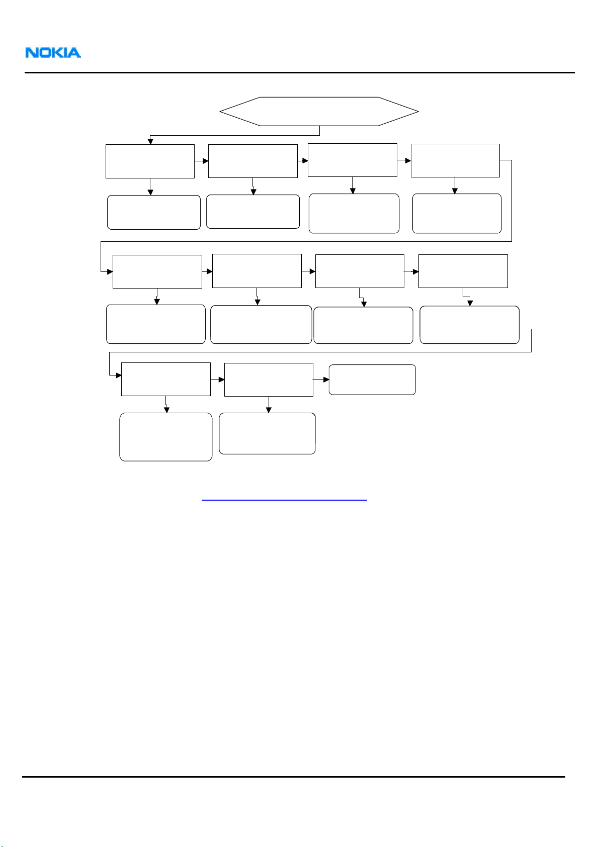
:
:
:
:
:
:
k
:
:
Nokia Customer Care
ST_CDSP_RF_SUPPLY_TEST
ST_CDSP_RF_SUPPLY_TES
HINKU ERRORS
HINKU ERRORS
Appendix A: RF Troubleshooting
VB_EXT Fail
VB_EXT fail
(0x0001)
Faulty capacitor at VDDLNA1 pin
(0x0001)
YES
YES
Propable cause:
Propable cause:
Poor soldering in HINKU
Poor soldering in
VDDLNA1 Fail
(0x0010)
Propable cause:
Propable cause:
Poor solder in
Poor solder in HINKU
Other possible reasons
Other possible reasons:
RB_EXT or internal
RB_EXT or internal block
bias bloc
(0x0100)
Propable cause:
Propable cause:
Poor solder/Faulty Hinku
Poor solder/Faulty HINKU
Other possible reasons
Other possible reasons:
Wrong or missing resistor at
Hinku
VDDLNA1 Fail
(0x0010)
YES
YES
Hinku
(0x0100)
YES
YES
RB_ext pin
RB_ext pin
NO
NO
NO
NO
VDIG Fail
VDIG Fail
(0x0002)
Propable cause:
Propablecause:
Poor soldering in HINKU
Poor soldering inHinku
VDDLNA2 Fail
(0x0020)
Poor solder inHinku
Other possible reasons
Other possible reasons:
Faulty capacitor at VDDLNA2 pin
Faulty capacitor at VDDLNA2 pin
NO
NO
Temperature sensor
(0x0800)
Other possible reasons
Too hot or cold environment…
(0x0002)
YES
YES
VDDLNA2 Fail
(0x0020)
YES
YES
Propablecause:
Propable cause:
Poor solder in HINKU
Temperature sensor
(0x0800)
Propablecause:
Propable cause:
Faulty Hinku
Faulty HINKU
Other possible reasons:
VBAT1 or VR1 Fail
NO
NO
VBAT1or VR1 Fail
(0x0004)
Propablecause:
Propable cause:
Poor solder/FaultyHinku
Poor solder/Faulty HINKU
Other possible reasons
Other possible reasons:
Faulty capacitor at VR1
Faulty capacitor at VR1
NO
NO
VLO Fail
(0x0040)
Poor Solder in Hinku
Other possible reasons
Other possible reasons:
Faulty capacitor at VDDLNA2 pin
Faulty capacitor at VDDLNA1 pin
NO
NO
YES
YES
(0x0004)
YES
YES
VLO Fail
(0x0040)
YES
YES
Propable cause:
Propablecause:
Poor solder in HINKU
It’s not possible to get
here…
NO
NO
NO
NO
VMIX Fail
(0x0008)
YES
YES
VPRE Fail
(0x0080)
YES
YES
Hinku
Propable cause:
Propable cause:
Poor solder in Hinku
Poor solder in HINKU
Other possible reasons
Other possible reasons:
Faulty capacitor at VMIX pin
VPRE Fail
(0x0080)
Propable cause:
Propable cause:
Poor Solder in
Poor solder in HINKU
Other possible reasons
Other possible reasons:
Faulty capacitor at VLO pin
Faulty capacitor at VLO pin
NO
NO
Please, refer to chapter
Error Code Interpretation Examples if more information about error code
interpretation is needed.
A-12
Company Confidential
Copyright © 2005 Nokia. All rights reserved
Page 71

A
Appendix A: RF Troubleshooting
2.3 TX IQ self test (ST_CDSP_TX_IQ_TEST)
TX_IQ_TEST (85) checks that the TXIQ lines between RAP & Vinku are properly connected. If this fails
also power tests and RXIQ loopback will fail.
Tested signals: VBAT_ASIC, TXIP, TXIQ, TXQP, TXQN, DAC_REF1, RFBUS
Error code for this self test is given in format:
• 0xyy, 0xzz, MeasResult1, MeasResult2, …
,where 0xyy, 0xzz is the main part of the error code: 0xyyzz
Nokia Customer Care
ST_CDSP_TX_IQ_TEST
ERRORS
ALL or ANY ERROR
(0x00xx)
YES
Propable cause:
Poor soldering/faulty
VINKU
Poor soldering/faulty RAP
Other possible reasons:
RETU, but since we’ve
gotten this far
without fails it should be
OK
-13
Company Confidential
Copyright © 2005 Nokia. All rights reserved
Page 72

Nokia Customer Care
2.4 TXC Data test (ST_TXC_DATA_TEST)
TXC_DATA_TEST (74) tests that the TXC line between RETU & VINKU is properly connected. If this fails
also TX power tests will fail.
Test covers: TxC power control signal, Retu (N2200), RFBUS, Vinku (N7501), VBAT_ASIC
Error code for this self test is given in format:
• 0xyy, 0xzz, MeasResult1, MeasResult2, …
,where 0xyy, 0xzz part is the main part of the error code: 0xyyzz
ST_CDSP_TXC_DATA_TEST
ERRORS
Appendix A: RF Troubleshooting
TXC too high at min
input (0x0001)
Propable cause:
Faulty RETU
Other possible reasons:
Vinku, but it only routes the
voltage back to RETU so in this
test, so it’s very unlikely.
YES
NO
TXC too low at max
input (0x0002)
Propable cause:
Poor soldering/Faulty VINKU
Poor soldering/Faulty RETU
YES
NO
It’s not possible to
get here…
A-14
Company Confidential
Copyright © 2005 Nokia. All rights reserved
Page 73

A
)
Appendix A: RF Troubleshooting
2.5 WCDMA power detector biasing self test (ST_CDSP_PWR_DETECTOR_BIAS_TEST)
POWER_DETECTOR_BIAS_TEST (82) tests the biasing of the power detector.
If this fails, also the power tests will fail/can’t be trusted.
Test covers: Vinku (N7501) WCDMA power detector biasing circuit functionality, Retu (N2200) WTXDET
input. RFBUS, VBAT_ASIC
Error code for this self test is given in format:
• 0xyy, 0xzz, MeasResult1, MeasResult2
,where 0xyy, 0xzz part is the main part of the error code: 0xyyzz
Nokia Customer Care
ST_CDSP_WCDMA_POWER_DET
EC TOR_BIAS_TEST ERRORS
Test error (0x0001,
0x0002, 0x0008,
0x0010
YES
Propable cause:
?
Other possible reasons:
RFBUS, but shouldn’t be
since we’ve gotten this
far.
Please, refer to chapter
interpretation is needed.
Error Code Interpretation Examples if more information about error code
NO
Detector reading outside
limits (0x0004)
YES
Propable cause:
Problem in detector circuitry
see “WCDMA power detector
ok?” for debugging details.
Other possible reasons:
Poor solder/faulty Retu
NO
It’s not possible to
get here…
2.5.1 WCDMA power detector ok?
Follow these instructions if it’s needed to check WCDMA power detector functionality. Please notice
that WCDMA power detector is used only in maximum TX power limiting and WCDMA PA supply
voltage controlling purposes.
• WCDMA transmitter has to be active before measurements. Procedure is explained in chapter
“Transmitter troubleshooting”.
-15
Company Confidential
Copyright © 2005 Nokia. All rights reserved
Page 74

Nokia Customer Care
• Measurement can be done with an oscilloscope and a probe.
• Connect the probe to R7531.
• WTXDET signal should be constant DC-voltage. Voltage level should change if TX power is changed.
Vcontrol is lower on lower power levels and higher if higher power levels are used.
• WTXDET should be about 325 mV with power level +10 dBm, about 1.03 V with power level
+21 dBm and about 150 mV when power levels below 0 dBm are used.
• NOTICE: Perform WCDMA transmitter tests with > 0 dBm power only in RF shielded environment.
Appendix A: RF Troubleshooting
• If WTXDET –signal is not as expected follow the same troubleshooting instructions as in:
SMPS get correct control voltage from the WCDMA power detector (signal Vcontrol)?
Does
A-16
Company Confidential
Copyright © 2005 Nokia. All rights reserved
Page 75

A
:
g
Appendix A: RF Troubleshooting
2.6 RX PLL phase lock self test (ST_CDSP_RX_PLL_PHASE_LOCK_TEST)
RX_PLL_LOCK_TEST (79) tests the functionality of RX PLL. If this fails, none of the RX related
measurements cannot be trusted.
Tested signals: VBAT_ASIC, VDIG, VR1, VR1RX, VCP1, RFBUSDAT, RFBUSCLK, RFBUSENA, RXRESETX
Error code for this self test is given in format:
• 0xyy, 0xzz
,where 0xyy, 0xzz part is the total error code: 0xyyzz
Nokia Customer Care
Is t ere RF power at
h
Is there RF power at VCO
VCO output?
output?
YES
YES
Is RF power at Hinku
there
there RF power at
Is
in ut?
p
Hinku input?
YES
YES
there ENOUGH RF
Is
Is ere ENOUGH RF power
th
power at Hinku input?
at Hinku input?
I he RX VCO frequency
s t
Is t e Frequency correct ?
h
YES
YES
correct?
YES
YES
Hinku PLL not locked
Hinku PLL not locked
(0x0004)
(0x0004)
YES
YES
NO
NO
there supply voltage for VCO?
Is
If VR1RX is OK then the problem is
VCO, otherwise Hinku is faulty. (VR1
is routed through Hinku to VCO)
NO
NO
Propable cause:
Propable cause:
Poor solder/Faulty balun
Poor solder/Faulty balun
NO
NO
NO
NO
correct freq and
not locked then
Propable cause:
Balun or VCO
Propable cause:
Propable cause:
Correct frequency and Hinku
says it’s not locked then
change Hinku
ST_CDSP_RX_PLL_PHASE_LOCK_TE
ST_CDSP_RX_PLL_PHASE_LOCK_TE
NO
NO
YES
YES
Hinku says it’s
change Hinku
Propable cause:
Propable cause:
Poor solder/Faulty VCO
Poor solder/Faulty VCO
ERRORS
ST
Any other code It’s not possible to get
Any other code
YES
YES
NO
NO
Is CP1 voltage ok?
the V
Is the VCP voltage ok?
NO
NO
It’s not possible to
get here …
here…
Propable cause:
Propable cause:
Test problem
Test problem
RFBUS failure (but this
RFBUS failure (but this should
should be ok if we’ve
be ok if we’ve gotten this far)
otten this far)
Propable cause:
Propable cause:
Poor solder/ Faulty Hinku
Poor solder/Faulty Hinku
Other possible reasons
Other possible reasons:
VCP line shorted to ground
VCP line shorted to ground
YES
YES
Poor solder/Faulty RETU
Poor solder/Faulty RETU
NO
NO
Go through this and this link
c
not working change VCO
c ntrol voltage VC ok?” link
o
Hinku, if still not working
Hinku , if still
Propable cause:
Propable cause:
Propable cause:
Propable cause:
Go through “Are
if no help then
omponents near the RX
change
VCO ok?” and “RX VCO
f no help then change
i
change VCO.
-17
Company Confidential
Copyright © 2005 Nokia. All rights reserved
Page 76

:
g
g
Nokia Customer Care
2.7 TX PLL phase lock self test (ST_CDSP_TX_PLL_PHASE_LOCK_TEST)
TX_PLL_LOCK_TEST (80) tests the functionality of RX PLL. If this fails also the TX power tests will fail.
Tested signals: VBAT_ASIC, VDIG, VR1, VCP2, RFBUSDAT, RFBUSCLK, RFBUSENA, TXRESETX
Error code for this self test is given in format:
• 0xyy, 0xzz
,where 0xyy, 0xzz part is the total error code: 0xyyzz
Appendix A: RF Troubleshooting
I there RF power at
s
Is there RF power at VCO
VCO output?
output?
YES
YES
I there RF power at
s
Is ere RF power at Vinku
th
Vinku input?
input?
YES
YES
Is there ENOUGH RF
Is there ENOUGH RF power
power at Vinku input?
at
Vinku input?
he TX VCO frequency
Is t
Is the Frequency correct ?
YES
YES
correct?
YES
YES
Vinku PLL not locked
Vinku PLL not locked
(0x0004)
(0x0004)
YES
YES
NO
NO
there supply
Is
Is there supply
voltage for VCO?
voltage
(VINKU VREG2)
NO
NO
Propable cause:
Propable cause:
Poor solder/Faulty balun
Poor solder/Faulty balun
NO
NO
NO
NO
correct freq and
Correct frequency and Hinku
Propable cause:
Propable cause:
Balun
Balun or VCO
Propable cause:
Propable cause:
not locked
then change Hinku
says it’s not locked then
change Hinku
ST_CDSP_TX_PLL_PHASE_LOCK_TE
ST_CDSP_TX_PLL_PHASE_LOCK
ST
NO
NO
for VCO?
YES
YES
Poor solder/Faulty VCO
Poor solder/Faulty VCO
ERROR
Any other code
Any other code
YES
YES
Propable cause:
Poor solder/Faulty Vinku
Propable cause:
Other possible reasons:
Poor solder/ Faulty Vinku
(This should have already
(This should have already
failed in earlier tests)
failed in earlier tests)
Propable cause:
Propable cause:
NO
NO
or VCO
Hinku says it’s
Is the VCP2 voltage ok?
Is the VCP voltage ok?
It’s not possible to get
NO
NO
It’s not possible to
here…
get here …
Propable cause:
Test problem
RFBUS failure (but this
should be ok if we’ve
otten this far)
round
TX VCO
VCO.
Propable cause:
Propable cause:
Poor solder/Faulty RETU
Poor solder/Faulty RETU
Other possible reasons
Other possible reasons:
VCP line shorted to ground
VCP line shorted to
NO
NO
Propable cause:
Propable cause:
Check the loop components/
Check the loop
YES
YES
solder joints, if no help, change
components/solder joints, if
Vinku
. If still not working, change
no help, change Vinku. If
still not working, change TX
A-18
Company Confidential
Copyright © 2005 Nokia. All rights reserved
Page 77

A
g
)
Appendix A: RF Troubleshooting
2.8 WCDMA transmitter self test (ST_CDSP_WCDMA_TX_POWER_TEST)
TX_WCDMA_POWER_TEST (75) checks the output power of the WCDMA transmitter.
Test covers: Modulator, Vinku (N7501) IC gain stages, IC output supply components, TX filter, WCDMA
PA (N7503), DCDC-converter (N7504), RFBUS, VBAT_ASIC, VBAT_PA
Nokia Customer Care
Test does not cover: Circulator (Z7505), duplexer (Z7502), and antenna
To prevent network interference, the phone must be in an RF shield box, when this test is run!
Error code for this self test is given in format:
• 0xyy, 0xzz, MeasResult1, MeasResult2
,where 0xyy, 0xzz part is the main part of the error code: 0xyyzz
ST_CDSP_WCDMA_TX_POWER_TEST
ST_CDSP_WCDMA_TX_POWER_TEST
Too low output power
Too low output power
(0x0010)
(0x0010)
YES
YES
NO
NO
Any other code
Any other code
YES
YES
It’s not possible to
NO
NO
It’s not possibleto
get here…
get here
…
ny power at Vinku
A
Any power at Vinku output
output at all?
at all ?
YES
YES
Propable cause:
Propable cause:
Plenty of components
Plenty of components involved. Go
involved. Go through the whole
thro
ugh the whole “WCDMA TX
“WCDMA TX power and transmit
o
p wer and transmit frequency
Frequency ok?”
to find reason.
ok?” to find reason.
NO
NO
Propable cause:
Propablecause:
Poor solder/Faulty Vinku
Poor solder/FaultyVinku
Propablecause:
Propable cause:
Test problem
Test problem
RFBUS failure (but this should
RFBUS failure (but this
be ok if we’ve gotten this far)
should be ok if we’ve
otten this far
-19
Company Confidential
Copyright © 2005 Nokia. All rights reserved
Page 78
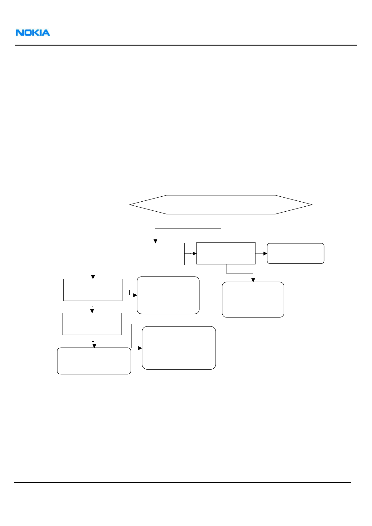
:
:
Nokia Customer Care
2.9 RX IQ loop back self test (ST_CDSP_RX_IQ_LOOP_BACK_TEST)
RX_IQ_LOOPBACK (81) tests that the RXI lines & VREFCM line between RAP & HINKU are connected.
Tested signals: VBAT_ASIC, RXQP, RXQN, RXIP, RXIN, VREFCM, TXIP, TXIN, RFBUS
Error code for this self test is given in format:
• 0xyy, 0xzz, MeasResult1, MeasResult2
,where 0xyy, 0xzz part is the main part of the error code: 0xyyzz
ST_CDSP_RX_IQ_LOOP_BACK_TEST
ST_CDSP_RX_IQ_LOOP_BACK_TEST
Appendix A: RF Troubleshooting
A IQ signals OK?
re RX
Are RXIQ signals OK?
VREFCM OK?
VREFCM OK?
Propable cause:
Propable cause:
Poor solder/Faulty RAP
Poor solder/Faulty RAP
Measured IQ power
Measured IQ power
under limit
(0x0010)
NO
NO
YES
YES
NO
YES
YES
NO
under limit
(0x0010)
YES
YES
Propable cause:
Propable cause:
Poor solder/Faulty Hinku
Poor solder/Faulty Hinku
Other possible reasons:
Other possible reasons
Vinku, but it should have
Vinku, but it should have
failed already in earlier
failed already in earlier
Retu/VB_ext line, but these should
tests
Propable cause:
Propable cause:
Poor solder/Faulty Hinku
Poor solder/Faulty Hinku
Other possible reasons:
Other possible reasons
Retu/VB_ext line, but these
should have failed already in
have failed already
earlier tests.
in earlier tests
NO
NO
Any other code
Any other code
YES
YES
Propable cause:
Propable cause:
Test problem
RFBUS failure (but this
RFBUS failure (but this should
should be ok if we’ve
be ok if we’ve gotten this
gotten this far)
NO
NO
Test problem
It’s not possible to get
It’s not possible to
get here
here…
…
A-20
Company Confidential
Copyright © 2005 Nokia. All rights reserved
Page 79

A
Appendix A: RF Troubleshooting
2.10 GSM transmitter self test (ST_CDSP_GSM_TX_POWER_TEST)
Nokia Customer Care
TX_GSM_POWER_TEST (77) checks the output power of the GSM transmitter.
Test covers: RFIC Vinku (N7501), modulator, IC gain control stages, filter/balun solder joints, GSM PA
(N7502), PA bias lines & DACs, RFBUS, TX power detector functionality, VBAT_ASIC, VBAT_PA.
Test does not cover: Antenna functionality, RX/TX-switch functionality, and TX signal quality
Error code for this self test is given in format:
• 0xyy, 0xzz, MeasResult1, MeasResult2, …
,where 0xyy, 0xzz part is the main part of the error code: 0xyyzz
-21
Company Confidential
Copyright © 2005 Nokia. All rights reserved
Page 80
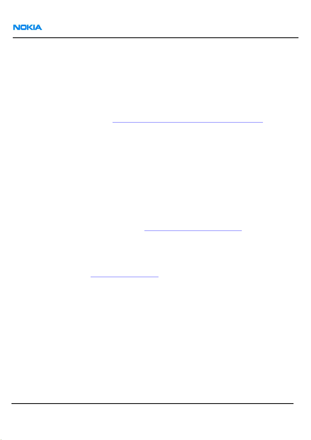
Nokia Customer Care
2.11 Error Code Interpretation Examples
This section presents three different examples of RF error code interpretation.
2.11.1 Example 1
ST_CDSP_RX_PLL_PHASE_LOCK self test gives “Fatal” result with error code: 0x00, 0x04
This means that the total error code is “0x004” (“0000 0000 0000 0100” in binary format) and if we
look a flowchart in section
for the code is “Hinku PLL is not locked”.
2.11.2 Example 2
Some of the self-tests can return multiple errors at the same time.
For example: RF-BB interface (ST_CDSP_RF_BB_IF_TEST) self test gives “Fatal” result with
error code: 0x00, 0x09, …
Appendix A: RF Troubleshooting
RX PLL phase lock self test (ST_CDSP_RX_PLL_PHASE_LOCK_TEST) the meaning
This means that the total error code without measurement values is “0x0009” and this is the same as
“0000 0000 0000 1001” in binary format. If we look closer there are multiple errors (2) found:
Bit mask “---- ---- ---- ---1” = “0x0001”
Bit mask “---- ---- ---- 1---“ = “0x0008”
Troubleshooting can be continued with
there are errors with two error codes: 0x0001 and 0x0008.
2.11.3 Example 3
Supply test for Hinku and Vinku (ST_CDSP_RF_SUPPLY_TEST) is slightly different self test from others
because there are both Vinku and Hinku errors shown in the same error code (
explained in section
For example: ST_CDSP_RF_SUPPLY_TEST gives “Fatal” result with error code: 0x0B, 0xBC, 0x00, 0x00, …
This error code means that there are probably no errors in Hinku RX ASIC supply voltages because the
main part of the error code for Hinku is 0x00, 0x00 (=0x0000) and means the same as “no errors”.
Anyway, there are many errors with Vinku TX ASIC supply voltages. The main part of the error code for
Vinku is 0x0B, 0xBC and that’s the same as “101110111100” in binary format. If we look closer there
are multiple (8) errors found:
RF-BB interface (ST_CDSP_RF_BB_IF_TEST) flowchart because
The format for error code is
Supply test for Hinku and Vinku).
A-22
Bit mask “---- ---- ---- -1--“ = “0x0004”
Bit mask “---- ---- ---- 1---“ = “0x0008”
Bit mask “---- ---- ---1 ----“ = “0x0010”
Bit mask “---- ---- --1- ----“ = “0x0020”
Company Confidential
Copyright © 2005 Nokia. All rights reserved
Page 81

A
Appendix A: RF Troubleshooting
Bit mask “---- ---- 1--- ----“ = ”0x0080”
Bit mask “---- ---1 ---- ----“ = “0x0100”
Bit mask “---- --1- ---- ----“ = ”0x0200”
Bit mask “---- 1--- ---- ----“ = ”0x0800”
Nokia Customer Care
Troubleshooting can be continued with
ST_CDSP_RF_SUPPLY_TEST VINKU flowchart because there are
errors with eight VINKU error codes.
Typically this kind of error occurs if there is no VBAT_ASIC voltage coming to the Vinku TX ASIC at all or
the ASIC is poorly soldered to the PWB (All voltages that are somehow related to VBAT_ASIC are
causing errors).
-23
Company Confidential
Copyright © 2005 Nokia. All rights reserved
Page 82

Nokia Customer Care
3. DOES THE PHONE REGISTER TO THE NETWORK AND MAKE A CALL (GSM)?
• Test against a GSM communication tester or real GSM network with a proper SIM.
3.1 GSM transmitter power levels and transmit frequency ok?
• Attach the phone to the product specific test jig and a spectrum analyser to the RF-coupler.
Coupler attenuation should be also taken into account during measurements.
• Set GSM Tx ON. Procedure is explained in section “Transmitter troubleshooting”.
• Spectrum analyser centre frequency should be set according the used TX channel (See section
“Frequency mappings”).
• Spectrum analyser RBW = VBW = 1 MHz, Span 0 MHz, sweep time 1 ms. Notice that GSM
transmission has pulsed nature and power should be measured during TX burst (triggering
needed). Another possibility is to use following settings: RBW = VBW = 1 MHz, Span 200 kHz and
sweep time at least 2.5 seconds.
Appendix A: RF Troubleshooting
• Test at least the maximum and minimum power levels:
- EGSM900: The maximum power level is “5” (31 – 34 dBm, typ. value +33 dBm)
The minimum power level is “19” (3 – 7 dBm, typ. value +5 dBm)
- GSM1800: The maximum power level is “0” (28 – 32 dBm, typ. value +30 dBm)
The minimum power level is “15” (-2 - +2 dBm, typ. value +0 dBm)
- GSM1900: The maximum power level is “0” (28 – 32 dBm, typ. value +30 dBm)
The minimum power level is “15” (-2 - +2 dBm, typ. value +0 dBm)
• If power is not as expected separate the phone into parts and place to the module jig. Connect the
spectrum analyser to the module jig GSM RF connector and measure power levels again (Notice
that there are three antenna connectors in the module jig, one for GSM, one for WCDMA and one for
Bluetooth. Make sure that all connections are made to the correct RF-connector).
- Power levels ok in the module jig: Antenna or antenna connection bad. Replace the antenna
- Power levels still wrong or no TX signal found at all: Continue troubleshooting
• If TX signal is not found at all use wider span setting and check if the transmitter is transmitting
on wrong frequency. If the signal is found to be on wrong frequency or frequency is not stabile,
see section
3.1.3. "GSM transmitter frequency correct".
3.1.1 Does GSM TX transmit RF-power at all?
A-24
Copyright © 2005 Nokia. All rights reserved
Company Confidential
Page 83

A
Appendix A: RF Troubleshooting
• If TX signal is not found at all use wider span setting and check if the transmitter is transmitting
on wrong frequency. If signal is found to be on wrong frequency or frequency is not stabile, see
section,
3.1.3. "GSM transmitter frequency correct".
3.1.1.1 Is Vinku (N7501) transmitting RF-power at all?
• GSM transmitter has to be active before Vinku’s output level can be measured. Procedure is
explained in section “Transmitter troubleshooting”.
• Measurements can be done with a spectrum analyser and an RF probe. RBW and VBW = 1 MHz,
Span = 0, sweep time 1 ms. Spectrum analyser centre frequency should be set according the used
TX channel (see section “Frequency mappings”). Notice that GSM transmission has pulsed nature
and power should be measured during TX burst (triggering needed). Another possibility is to use
following settings: RBW = VBW = 1 MHz, Span 200 kHz and sweep time at least 2.5 seconds.
• EGSM900:
- Connect the RF probe to Z7504 input. The level should be about the same on both input pins.
Check output level with at least the maximum (5) and the minimum (19) power levels.
Nokia Customer Care
- Maximum power level – Output level should be about -15…-25 dBm
- Minimum power level – Output level should be about -45…-55 dBm
• GSM1800/GSM1900:
- Connect the RF probe to C7577 or C7575. The level should be about the same on both capacitors.
Check output level with at least the maximum (0) and the minimum (15) power levels.
- Maximum power level – Output level should be about -25…-35 dBm
- Minimum power level – Output level should be about -55…-65 dBm
• Check if output levels of Vinku are as expected.
• NOTE! If VINKU output RF-power is totally missing just in one or two GSM-bands, typically this
means that Vinku ASIC (N7501) is faulty or the ASIC is badly soldered. For example: VINKU is not
transmitting at all in EGSM900-band but TX-power is ok in other GSM-bands. Then it’s quite clear
that VINKU (N7501) is faulty or badly soldered and the component should be replaced.
3.1.1.1.1 RF operating voltage VBAT_ASIC?
• Measurement can be done with an oscilloscope and a probe.
• Connect the probe to C7503 (or C7501, C7541)
• VBAT_ASIC voltage level should be 3.05 – 5.4 V. Typical value is 4.0 V.
3.1.1.1.1.1 Ferrite inductor L7503 ok?
• Check that component is in place and solder joints are ok
• Measure voltage from the both ends of L7503. Is it faulty or is there short circuit in RF end?
-25
Company Confidential
Copyright © 2005 Nokia. All rights reserved
Page 84
Nokia Customer Care
• Disconnect the power supply from the phone and use an ohmmeter to check that inductor is
conducting DC.
3.1.1.1.2 RFBUS signals ok?
• GSM receiver has to be active before RFBUS signals can be measured. Procedure is explained in
section “GSM RX chain activation for manual measurements”. Also WCDMA/GSM transmitter and
WCDMA receiver activation can be used for the measurement but then RFBUS -signals don’t
necessarily look like in figures mentioned below.
• Measurements can be performed with an oscilloscope and a probe. Check all five RF BUS signals:
- RFBUSDAT: Connect the probe to J7504. Typical RFBUSDAT -signal is shown in section 6.5.9.3
RFBUSDAT (GSM RX)”
“
- RFBUSCLK: Connect the probe to J7505. Typical RFBUSCLK -signal is shown in sections 6.5.9.1
RFUSCLK (GSM RX)” and 6.5.9.2 “RFBUSCLK and RFBUSENA (GSM RX)”
“
- RFBUSENA: Connect the probe to J7506. Typical RFBUSENA -signal is shown in section 6.5.9.2
RFBUSCLK and RFBUSENA (GSM RX)”
“
Appendix A: RF Troubleshooting
- RXRESETX: Connect the probe to J7515. RXRESETX -signal is a constant 2 V DC-signal after GSM or
WCDMA transceiver has been activated the first time after phone boot up. The level of this signal
should be about 0 V before transceiver activation.
- TXRESETX: Connect the probe to J7517. TXRESETX -signal is a constant 2 V DC-signal after GSM or
WCDMA transceiver has been activated the first time after phone boot up. The level of this signal
should be about 0 V before transceiver activation.
3.1.1.1.2.1 RAP3G (or Vinku or Hinku) faulty?
• RAP3G (D2800) cannot be replaced.
3.1.1.1.3 Vinku (N7501) regulator voltages VREG1, VREG2 ok?
• GSM transmitter has to be active before VREG1 and VREG2 voltages can be measured. Procedure is
explained in section “Transmitter troubleshooting.”
• Measurements can be done with an oscilloscope and a probe.
• VREG1: Connect the probe to C7543
• VREG2: Connect the probe to C7548 (or C7547)
• VREG1 and VREG2 voltage levels should be 2.65 – 2.86 V. Typical value is 2.7 V.
3.1.1.1.3.1 Vinku (N7501) RB_EXT voltage ok?
• GSM transmitter has to be active before Vinku’s RB_EXT voltage can be measured. Procedure is
explained in section “Transmitter troubleshooting”.
A-26
Copyright © 2005 Nokia. All rights reserved
Company Confidential
Page 85

A
Appendix A: RF Troubleshooting
• Measurement can be done with an oscilloscope and a probe.
• Connect the probe to R7521.
• RB_EXT voltage should be 1.325 – 1.375 V.
3.1.1.1.3.1.1 VREFRF01-voltage ok?
• Measurement can be done with an oscilloscope and a probe.
• Connect the probe to R7503.
• VREFRF01 voltage should be 1.325 – 1.375 V. Typical value is 1.35 V.
3.1.1.1.3.1.1.1 Desolder R7503. Is VREFRF01 voltage still wrong?
• Remember to solder a new component to R7503 pads after the measurement.
3.1.1.1.3.1.1.1.1 Capacitors C7518, C7520 and C7570 working correctly?
Nokia Customer Care
• Check that components are in place and solder joints are ok
• Disconnect the power supply from the phone and use an ohmmeter to check that capacitors are
not short-circuited. If short-circuit is found replace capacitors mentioned above. If this does not
help go to the next step.
3.1.1.1.3.1.1.1.2 Replace Vinku (N7501) or Hinku (N7500) or both
3.1.1.1.3.1.2 R7521 and R7504 in place and working correctly?
• Check that components are in place and solder joints are ok
• Disconnect the power supply from the phone and check R7521 and R7504 resistance values with
an ohmmeter.
3.1.1.1.3.1.3 VB_EXT voltage ok?
• Measurement can be done with an oscilloscope and a probe.
• Connect the probe to C7518.
• VB_EXT voltage should be 1.325 – 1.375 V. Typical value is 1.35 V.
3.1.1.1.3.1.3.1 Is R7503 in place and working correctly?
• Check that the component is in place and solder joints are ok
• Disconnect the power supply from the phone and check R7503 resistance value with an ohmmeter
3.1.1.1.3.1.3.2 Capacitors C7518, C7520 and C7570 working correctly?
• Check that components are in place and solder joints are ok
• Disconnect the power supply from the phone and use an ohmmeter to check that capacitors are
not short-circuited. If short-circuit is found replace capacitors mentioned above. If this does not
Company Confidential
Copyright © 2005 Nokia. All rights reserved
-27
Page 86

Nokia Customer Care
Appendix A: RF Troubleshooting
help go to the next step.
3.1.1.1.3.1.3.3 Replace Vinku (N7501) or Hinku (N7500) or both
3.1.1.1.3.1.4 Replace Vinku (N7501)
3.1.1.1.3.2 Are capacitors in Vinku (N7501) regulator lines working correctly?
VREG1: C7543
VREG2: C7547, C7548, C7554, C7555, C7553, C7552, C7558 and C7567
• Check that components are in place and solder joints are ok
• Disconnect the power supply from the phone and use an ohmmeter to check that regulator lines
are not short-circuited to the ground. If short-circuit is found replace capacitors mentioned above.
If this does not help go to the next step.
3.1.1.1.3.3 TX VCO (G7502) ok?
3.1.1.1.3.4 Replace Vinku (N7501)
3.1.1.1.4 VXO-voltage ok? (=Vdig).
• Measurement can be done with an oscilloscope and a probe
• Connect the probe to C7560 (or C7526, C7513) Notice: C7526 is a non-assembled component so the
probe should be connected to the pad that can still be found from the PWB.
• VXO-voltage should be about 2.5 V
3.1.1.1.4.1 C7560, C7513, C7526 and C2214 ok?
• Check that components are in place and solder joints are ok
• Notice: C7526 is a non-assembled component so the probe should be connected to the pad that
can still be found from the PWB.
• Disconnect the power supply from the phone and use an ohmmeter to find out if the VXO-line is
short-circuited to the ground. If short-circuit is found replace C7560, C7513, C7526 and C2214. If
replacing does not help then go to the next steps.
3.1.1.1.4.2 Replace Retu
3.1.1.1.4.3 Replace Hinku (N7500) or Vinku (N7501) or VCTCXO (G7501) or all three components
3.1.1.1.5 VCP2-voltage ok?
• GSM transmitter has to be active before VCP2 voltage can be measured. Procedure is explained in
section “Transmitter troubleshooting”.
• Measurement can be done with an oscilloscope and a probe.
A-28
Company Confidential
Copyright © 2005 Nokia. All rights reserved
Page 87

A
Appendix A: RF Troubleshooting
• Connect the probe to C2221 (or C7550).
• VCP2 voltage should be about 4.75 V.
3.1.1.1.5.1 C7550 and C2221 working correctly?
• Check that components are in place and solder joints are ok
• Disconnect the power supply from the phone and use an ohmmeter to find out if the VCP2-line is
short-circuited to the ground. If short-circuit is found replace C7550 and C2221. If this does not
help go to the next steps.
3.1.1.1.5.2 Retu ok?
3.1.1.1.5.3 Vinku (N7501) ok?
3.1.1.1.6 Is there RF power in the TX VCO output at all?
• GSM transmitter has to be active before TX VCO’s output frequency and output level can be
measured. Procedure is explained in section “Transmitter troubleshooting”.
Nokia Customer Care
• Measurements can be done with a spectrum analyser and an RF probe. Spectrum analyser centre
frequency should be set according the used TX channel (see section “Frequency mappings”).
• Spectrum analyser RBW and VBW = 1 MHz, Span = 0, sweep time 1 ms. Notice that GSM
transmission has pulsed nature and VCO output power should be measured during TX burst
(triggering needed). Another possibility is to use following settings: RBW = VBW = 1 MHz, Span
200 kHz and sweep time at least 2.5 seconds.
• Connect the RF probe to the T7503 input. VCO shield has to be removed before measurement.
Remember to solder the shield back after the phone repairing. Quick VCO alive check can be done
also without removing the RF shield. The RF probe should be placed as near the TX VCO output as
possible (Put the head of the probe carefully inside the VCO can through the holes of the shield).
Remember to use low RF Attenuator value in the spectrum analyser with this method.
• Check if the frequency of the TX VCO is as expected. If the VCO signal is not found try to use wider
span setting. The correct VCO frequency can be found in section “Frequency mappings”. The
output level of the VCO should be about -25 dBm during GSM TX burst.
3.1.1.1.6.1 TX VCO operating voltage VREG2 (VR2) ok?
• See section
"Vinku (N7501) regulator voltages VREG1, VREG2 ok?"
3.1.1.1.6.2 Replace TX VCO (G7502)
3.1.1.1.7 Is TX VCO RF-signal coming to the Vinku at all?
• GSM transmitter has to be active before TX VCO’s output level can be measured. Procedure is
explained in section “Transmitter troubleshooting”.
• Measurements can be done with a spectrum analyser and an RF probe. Spectrum analyser centre
frequency should be set according the used TX channel (see section “Frequency mappings”).
• Spectrum analyser RBW and VBW = 1 MHz, Span = 0, sweep time 1 ms. Notice that GSM
Copyright © 2005 Nokia. All rights reserved
-29
Company Confidential
Page 88
Nokia Customer Care
transmission has pulsed nature and VCO output power should be measured during TX burst
(triggering needed). Another possibility is to use following settings: RBW = VBW = 1 MHz, Span
200 kHz and sweep time at least 2.5 seconds.
• Check the level of the TX VCO frequency in T7503 outputs. The level should be about -30…-35 dBm
in both output lines. If the signal level is correct in the input (about -25 dBm) but output level is
not as expected then replace T7503. VCO shield has to be removed before measurement.
Remember to solder the shield back after the phone repairing.
3.1.1.1.7.1 Replace balun T7503
3.1.1.1.8 Are TX-IQ signals ok?
• These current mode signals are not possible to measure, but are tested with self-tests. So if there
is no fail in 2.3. “
ST_CDSP_TX_IQ_TEST” these signals should be ok. Otherwise Vinku (N7501) or
RAP3G (D2800) is faulty. Notice that it is not possible to replace RAP3G ASIC.
3.1.1.1.9 Is there TXC-signal coming to Vinku ASIC (N7501)?
Appendix A: RF Troubleshooting
• GSM transmitter has to be active before TX control voltage TXC can be measured. Procedure is
explained in section “Transmitter troubleshooting”.
• Set TX power level first to the maximum (“5” in EGSM900 and “0” in GSM1800/GSM1900)
• Measurement can be done with an oscilloscope and a probe.
• Connect the probe to C7549
• Typical TX control voltage TXC timing should look somehow similar to figure
6.5.2 "TXC in GSM
mode (DC Offset 0 V)" (EGSM900 TX power level 5) and voltage levels should be roughly:
- EGSM900: 1.8 V while TX burst and 0 V otherwise.
- GSM1800/GSM1900: 1.8 V while TX burst and 0 V otherwise.
• Change the TX to the minimum power level (“19” in EGSM and “15” in GSM1800/GSM1900)
• Typical TX control voltage TXC levels should be now about:
- EGSM900: 1.0 V while TX burst and 0 V otherwise.
- GSM1800/GSM1900: 0.7 V while TX burst and 0 V otherwise.
3.1.1.1.9.1 R7514 in place?
• Check that the component is in place and solder joints are ok
• Disconnect the power supply from the phone and check R7514 resistance value with an ohmmeter
3.1.1.1.9.2 C7549 working correctly?
• Check that the component is in place and solder joints are ok
• Disconnect the power supply from the phone and use an ohmmeter to check that C7549is not
A-30
Copyright © 2005 Nokia. All rights reserved
Company Confidential
Page 89

A
Appendix A: RF Troubleshooting
short-circuited. If short-circuit is found replace the capacitor.
3.1.1.1.9.3 Retu ok?
3.1.1.1.10 VCTCXO frequency and output level correct?
• Measurement can be done with an oscilloscope and a probe.
• Connect the probe to C7529 (or C7582)
• The frequency of the VCTCXO should be quite exactly 38.4 MHz and level about 0.5 - 0.9 Vpp.
Example of the correct VCTCXO output signal is presented in figure
1.24 V)"..
3.1.1.1.10.1 VXO-voltage ok? (=Vdig).
• Measurement can be done with an oscilloscope and a probe
• Connect the probe to C7560 (or C7526, C7513) Notice: C7526 is a non-assembled component so the
probe should be connected to the pad that can still be found from the PWB.
Nokia Customer Care
6.5.1. "VCTCXO Output (DC Offset
• VXO-voltage should be about 2.5 V
3.1.1.1.10.1.1 C7560, C7513, C7526 and C2214 ok?
• Check that components are in place and solder joints are ok
• Notice: C7526 is a non-assembled component so the probe should be connected to the pad that
can still be found from the PWB.
• Disconnect the power supply from the phone and use an ohmmeter to find out if the VXO-line is
short-circuited to the ground. If short-circuit is found replace C7560, C7513, C7526 and C2214. If
replacing does not help then go to the next steps.
3.1.1.1.10.1.2 Replace Retu
3.1.1.1.10.1.3 Replace Hinku (N7500) or Vinku (N7501) or VCTCXO (G7501) or all three components
3.1.1.1.10.2 BB AFC-voltage ok?
• See section
"BB AFC-voltage ok?"
3.1.1.1.10.3 Replace VCTCXO G7501
3.1.1.1.11 Replace Vinku (N7501)
3.1.1.2 Is there RF-power in the GSM PA (N7502) input at all?
• GSM transmitter has to be active before measurements. Procedure is explained in section
“Transmitter troubleshooting”.
• Set TX power level to the maximum (“5” in EGSM900 and “0” in GSM1800/GSM1900)
• Measurements can be done with a spectrum analyser and an RF probe. Remember to make correct
Company Confidential
Copyright © 2005 Nokia. All rights reserved
-31
Page 90
Nokia Customer Care
Appendix A: RF Troubleshooting
frequency settings to the spectrum analyser. Spectrum analyser centre frequency should be set
according the used TX channel (see section “Frequency mappings”).
• Spectrum analyser RBW and VBW = 1 MHz, Span = 0, sweep time 1 ms. Notice that GSM
transmission has pulsed nature and power should be measured during TX burst (triggering
needed). Another possibility is to use following settings: RBW = VBW = 1 MHz, Span 200 kHz and
sweep time at least 2.5 seconds.
• EGSM900: Connect the probe to J7521 (test point). The RF level should be roughly -15…-20 dBm.
• GSM1800 or GSM1900: Connect the probe to R7512 output. The RF level should be roughly -20…-
30 dBm.
3.1.1.2.1 EGSM900: Replace SAW Z7504
3.1.1.2.2 GSM1800/GSM1900: Is Vinku (N7501) output RF-signal coming to the T7502 (Balun)?
• GSM transmitter has to be active before measurements. Procedure is explained in section
“Transmitter troubleshooting”. Set TX power level to the maximum (“0” in GSM1800/GSM1900)
• Measurements can be done with a spectrum analyser and an RF probe. Spectrum analyser centre
frequency should be set according the used TX channel (see section “Frequency mappings”).
• Spectrum analyser RBW and VBW = 1 MHz, Span = 0, sweep time 1 ms. Notice that GSM
transmission has pulsed nature and power should be measured during TX burst (triggering
needed). Another possibility is to use following settings: RBW = VBW = 1 MHz, Span 200 kHz and
sweep time at least 2.5 seconds.
• GSM1800 or GSM1900: Connect the probe to T7502 input. There are two input ports in T7502
because the input port is balanced. The RF level should be roughly -25 dBm in both inputs.
3.1.1.2.2.1 Matching components ok?
GSM1800/GSM1900: C7575 and C7577
• Check that components are in place and solder joints are ok
• GSM1800 and GSM1900: Disconnect the power supply from the phone and use an ohmmeter to
check that capacitors C7575 and C7577 are not short-circuited. If short-circuit is found replace the
faulty capacitor.
3.1.1.2.3 GSM1800/GSM1900: Is there RF power in the balun (T7502) output at all?
A-32
• GSM transmitter has to be active before measurements. Procedure is explained in section
“Transmitter troubleshooting”. Set TX power level to the maximum (“0” in GSM1800/GSM1900)
• Measurements can be done with a spectrum analyser and an RF probe. Remember to make correct
frequency settings to the spectrum analyser. Spectrum analyser centre frequency should be set
according the used TX channel (see section “Frequency mappings”).
• Spectrum analyser RBW and VBW = 1 MHz, Span = 0, sweep time 1 ms. Notice that GSM
transmission has pulsed nature and power should be measured during TX burst (triggering
Company Confidential
Copyright © 2005 Nokia. All rights reserved
Page 91

A
Appendix A: RF Troubleshooting
needed). Another possibility is to use following settings: RBW = VBW = 1 MHz, Span 200 kHz and
sweep time at least 2.5 seconds.
• GSM1800 or GSM1900: Connect the probe to R7512 input. The RF level should be roughly -20…30 dBm.
3.1.1.2.3.1 Replace balun T7502
3.1.1.2.4 GSM1800/GSM1900: Replace attenuator R7512
3.1.1.3 Does GSM PA (N7502) transmit RF-power at all?
• GSM transmitter has to be active before measurements. Procedure is explained in section
“Transmitter troubleshooting”.
• Set TX power level to the minimum (“19” in EGSM900 and “15” in GSM1800/GSM1900)
• Measurements can be done with a spectrum analyser and an RF probe. Spectrum analyser centre
frequency should be set according the used TX channel (see section “Frequency mappings”).
Nokia Customer Care
• Spectrum analyser RBW and VBW = 1 MHz, Span = 0, sweep time 1 ms. Notice that GSM
transmission has pulsed nature and power should be measured during TX burst (triggering
needed). Another possibility is to use following settings: RBW = VBW = 1 MHz, Span 200 kHz and
sweep time at least 2.5 seconds.
• EGSM900: Connect the probe to J7520 (test point). The RF level should be about -16…-17 dBm.
• GSM1800 or GSM1900: Connect the probe to J7519 (test point). The RF level should be roughly
-29…-30 dBm in both bands.
3.1.1.3.1 GSM PA (N7502) operating voltage ok?
• Measurement can be done with an oscilloscope and a probe.
• Connect the probe to C7593
• Voltage level should be 3.05 – 5.4 V. Typical value is 4.0 V
3.1.1.3.1.1 PA operating voltage VBAT_PA ok?
• Measurement can be done with an oscilloscope and a probe.
• Connect the probe to C7569 (or C7564, C7583)
• Voltage level should be 3.05 – 5.4 V. Typical value is 4.0 V.
3.1.1.3.1.1.1 Ferrite Z7500 ok?
• Check that component is in place and solder joints are ok
• Disconnect the power supply from the phone and use an ohmmeter to check that inductor is
conducting DC.
3.1.1.3.1.2 C7593 ok?
-33
Company Confidential
Copyright © 2005 Nokia. All rights reserved
Page 92

Nokia Customer Care
• Check that the component is in place and solder joints are ok
• Disconnect the power supply from the phone and use an ohmmeter to check that the capacitor is
not short-circuited. If short-circuit is found replace the capacitor.
3.1.1.3.1.3 Replace inductor L7516
• If replacing does not help, replace GSM PA (N7502)
3.1.1.3.2 Are bias currents coming correctly to the GSM PA (N7502)?
EGSM: Icont_21 and Icont_22
GSM1800/GSM1900: Icont_31 and Icont_32
• GSM transmitter has to be active before measurements. Procedure is explained in section
“Transmitter troubleshooting”.
• Set TX power level to the maximum (“5” in EGSM900 and “0” in GSM1800/GSM1900)
Appendix A: RF Troubleshooting
• Measurements can be done with an oscilloscope and a VOLTAGE probe.
• EGSM900:
- Connect the probe to C7545 or C7544. Notice: C7544 is a non-assembled component so the probe
should be connected to the pad that can be still found from the PWB.
- Typical full TX power bias currents (Icont_21 and Icont_22) should look somehow similar to figure
6.5.4 "lcont_21/lcont_22 (DC offset 1.2V)" when measured with an oscilloscope and a probe. Check
both currents.
• GSM1800 or GSM1900:
- Connect the probe to C7561 or C7556.
- Typical full TX power bias currents (Icont_31 and Icont_32) should look somehow similar to figure
6.5.5 when measured with an oscilloscope and a probe. Check both currents.
3.1.1.3.2.1 Vinku (N7501) RB_EXT voltage ok?
• See section
"Vinku (N7501) RB_EXT voltage ok?"
3.1.1.3.2.2 Are capacitors in GSM PA (N7502) bias lines working correctly?
EGSM: Icont_21 missing – Replace Vinku
Icont_22 missing – C7545 short-circuited?
GSM1800/GSM1900: Icont_31 missing – C7556 short-circuited?
Icont_32 missing – C7561 short-circuited?
• Check that components are in place and solder joints are ok
• Disconnect the power supply from the phone and use an ohmmeter to check that capacitors are
not short-circuited. If short-circuit is found replace capacitors mentioned above. If this does not
A-34
Company Confidential
Copyright © 2005 Nokia. All rights reserved
Page 93

A
Appendix A: RF Troubleshooting
help go to the next step.
3.1.1.3.2.3 Replace Vinku (N7501)
3.1.1.3.3 Replace PA (N7502)
3.1.1.4 Are control voltages VC1, VC2 and VC3 coming correctly to the antenna switch (Z7503)?
• Use “RF Controls” window in Phoenix test software to activate the GSM transmitter and to select
the wanted GSM band. Procedure is explained in section “Transmitter troubleshooting”. GSM RX
activation is described in section “GSM RX chain activation for manual measurements”.
• Use an oscilloscope and probe to find out if antenna switch control lines are working according to
table shown below. “Hi” means that there is 2.4 – 2.8 V control voltage level in the corresponding
control line. “Lo” means levels 0 – 0.2 V. Remember to trigger the oscilloscope because control
voltages VC1, VC2 and VC3 are pulsed
• Connect the probe to correct test points to measure VC1, VC2 and VC3 voltages (check test point
locations from section “Test point locations”). Notice: these test points are PWB pads for three
non-assembled capacitors.
Nokia Customer Care
3.1.1.4.1 Replace Hinku (N7500)
3.1.1.5 Replace antenna Switch Z7503
3.1.2 Does GSM TX transmit enough RF-power and power levels otherwise ok?
3.1.2.1 Is Vinku ASIC (N7501) transmitting correct RF-power?
• GSM transmitter has to be active before Vinku’s output level can be measured. Procedure is
explained in section “Transmitter troubleshooting”.
• Measurements can be done with a spectrum analyser and an RF probe. RBW and VBW = 1 MHz,
Span = 0, sweep time 1 ms. Spectrum analyser centre frequency should be set according the used
TX channel (see section “Frequency mappings”). Notice that GSM transmission has pulsed nature
and power should be measured during TX burst (triggering needed). Another possibility is to use
following settings: RBW = VBW = 1 MHz, Span 200 kHz and sweep time at least 2.5 seconds.
• EGSM900:
- Connect the RF probe to Z7504 input. The level should be about the same on both input pins.
Check output level with at least the maximum (5) and the minimum (19) power levels.
-35
Company Confidential
Copyright © 2005 Nokia. All rights reserved
Page 94
Nokia Customer Care
- Maximum power level – Output level should be about -15…-25 dBm
- Minimum power level – Output level should be about -45…-55 dBm
• GSM1800/GSM1900:
- Connect the RF probe to C7577 or C7575. The level should be about the same on both capacitors.
Check output level with at least the maximum (0) and the minimum (15) power levels.
- Maximum power level – Output level should be about -25…-35 dBm
- Minimum power level – Output level should be about -55…-65 dBm
• Check if output levels of Vinku are as expected.
• NOTE! If VINKU ASIC is transmitting wrong TX power just in one or two GSM-bands, typically
this means that Vinku ASIC (N7501) is faulty or the ASIC is badly soldered. Of course SAW-filter
Z7504 or balun T7502 can be also faulty/badly soldered and causing short-circuit, but probability
to this is quite low. For example: VINKU is transmitting too low power in EGSM900-band but TXpower is ok in other GSM-bands. Then it’s almost clear that VINKU (N7501) is faulty or badly
soldered and the component should be replaced.
Appendix A: RF Troubleshooting
3.1.2.1.1 RF operating voltage VBAT_ASIC ok?
• See section
“RF operating voltage VBAT_ASIC ok?”
3.1.2.1.2 Are Vinku (N7501) regulator voltages VREG1, VREG2 ok?
• GSM transmitter has to be active before VREG1 and VREG2 voltages can be measured. Procedure is
explained in section “Transmitter troubleshooting”.
• Measurements can be done with an oscilloscope and a probe.
• VREG1: Connect the probe to C7543
• VREG2: Connect the probe to C7548 (or C7547)
• VREG1 and VREG2 voltage levels should be 2.65 – 2.86 V. Typical value is 2.7 V.
3.1.2.1.2.1 Vinku (N7501) RB_EXT voltage ok?
• GSM transmitter has to be active before Vinku’s RB_EXT voltage can be measured. Procedure is
explained in section “Transmitter troubleshooting”.
• Measurement can be done with an oscilloscope and a probe.
• Connect the probe to R7521.
• RB_EXT voltage should be 1.325 – 1.375 V.
3.1.2.1.2.1.1 VREFRF01-voltage ok?
• Measurement can be done with an oscilloscope and a probe.
A-36
Company Confidential
Copyright © 2005 Nokia. All rights reserved
Page 95

A
Appendix A: RF Troubleshooting
• Connect the probe to R7503.
• VREFRF01 voltage should be 1.325 – 1.375 V. Typical value is 1.35 V.
3.1.2.1.2.1.1.1 Desolder R7503. Is VREFRF01 voltage still wrong?
• Remember to solder a new component to R7503 pads after the measurement.
3.1.2.1.2.1.1.1.1 Capacitors C7518, C7520 and C7570 working correctly?
• Check that components are in place and solder joints are ok
• Disconnect the power supply from the phone and use an ohmmeter to check that capacitors are
not short-circuited. If short-circuit is found replace capacitors mentioned above. If this does not
help go to the next step.
3.1.2.1.2.1.1.1.2 Replace Vinku (N7501) or Hinku (N7500) or both
3.1.2.1.2.1.2 R7521 and R7504 in place and working correctly?
Nokia Customer Care
• Check that components are in place and solder joints are ok
• Disconnect the power supply from the phone and check R7521 and R7504 resistance values with
an ohmmeter.
3.1.2.1.2.1.3 VB_EXT voltage ok?
• Measurement can be done with an oscilloscope and a probe.
• Connect the probe to C7518.
• VB_EXT voltage should be 1.325 – 1.375 V. Typical value is 1.35 V.
3.1.2.1.2.1.3.1 Is R7503 in place and working correctly?
• Check that the component is in place and solder joints are ok
• Disconnect the power supply from the phone and check R7503 resistance value with an ohmmeter
3.1.2.1.2.1.3.2 Capacitors C7518, C7520 and C7570 working correctly?
• Check that components are in place and solder joints are ok
• Disconnect the power supply from the phone and use an ohmmeter to check that capacitors are
not short-circuited. If short-circuit is found replace capacitors mentioned above. If this does not
help go to the next step.
3.1.2.1.2.1.3.3 Replace Vinku (N7501) or Hinku (N7500) or both
3.1.2.1.2.2 Replace Vinku (N7501)
3.1.2.1.3 Are TX-IQ signal waveforms looking correct?
• These current mode signals are not possible to measure, but are tested with self-tests. So if there
is no fail in 2.3
ST_CDSP_TX_IQ_TEST these signals should be ok. Otherwise Vinku (N7501) or RAP3G
Company Confidential
Copyright © 2005 Nokia. All rights reserved
-37
Page 96

Nokia Customer Care
Appendix A: RF Troubleshooting
(D2800) is faulty. Notice that it is not possible to replace RAP3G ASIC.
3.1.2.1.4 Is the TXC-signal coming to Vinku ASIC (N7501) OK? Is signal level correct?
• GSM transmitter has to be active before TX control voltage TXC can be measured. Procedure is
explained in section “Transmitter troubleshooting”.
• Set TX power level first to the maximum (“5” in EGSM900 and “0” in GSM1800/GSM1900)
• Measurement can be done with an oscilloscope and a probe.
• Connect the probe to C7549
• Typical TX control voltage TXC timing should look somehow similar to figure 6.5.2 “
mode (DC offset 0 V)” (EGSM900 TX power level 5) and voltage levels should be roughly:
- EGSM900: 1.8 V while TX burst and 0 V otherwise.
- GSM1800/GSM1900: 1.8 V while TX burst and 0 V otherwise.
• Change the TX to the minimum power level (“19” in EGSM and “15” in GSM1800/GSM1900)
• Typical TX control voltage TXC levels should be now about:
- EGSM900: 1.0 V while TX burst and 0 V otherwise.
• GSM1800/GSM1900: 0.7 V while TX burst and 0 V otherwise.
3.1.2.1.4.1 R7514 in place and working correctly?
• Check that the component is in place and solder joints are ok
• Disconnect the power supply from the phone and check R514 resistance value with an ohmmeter
3.1.2.1.4.2 C7549 working correctly?
• Check that the component is in place and solder joints are ok
TXC in GSM
• Disconnect the power supply from the phone and check with an ohmmeter that C7549 is not
short-circuited.
3.1.2.1.4.3 Retu ok?
3.1.2.1.5 Does GSM PA (N7502) get correct DET_SW_G -voltage from Vinku ASIC (N7501)?
• GSM transmitter has to be active before DET_SW_G voltage can be measured. Procedure is
explained in section “Transmitter troubleshooting”.
• Measurement can be done with an oscilloscope and a probe.
• Connect the probe to C7595 pad. Notice: C7595 is a non-assembled component so the probe
should be connected to the pad that can be still found from the PWB.
A-38
Company Confidential
Copyright © 2005 Nokia. All rights reserved
Page 97

A
Appendix A: RF Troubleshooting
• DET_SW_G voltage should be about 2.8 V while TX burst and 0 V otherwise.
3.1.2.1.5.1 C7595 working correctly?
• Check that the component is in place and solder joints are ok
• Disconnect the power supply from the phone and check with an ohmmeter that C7595 is not
short-circuited.
3.1.2.1.5.2 Replace Vinku (N7501)
3.1.2.1.6 Are components in GSM power control loop in place and working ok?
R7516 and C7559
• Disconnect the power supply from the phone and use an ohmmeter to check that C7559 is not
short-circuited. If short-circuit is found replace the capacitor.
Nokia Customer Care
• Check R7516 resistance value with an ohmmeter and replace resistor if needed.
3.1.2.1.7 Is TX VCO signal level in the T7503 output high enough?
• GSM transmitter has to be active before TX VCO’s output level can be measured. Procedure is
explained in section “Transmitter troubleshooting”.
• Measurements can be done with a spectrum analyser and an RF probe. RBW and VBW = 1 MHz,
Span = 0, sweep time 1 ms. Spectrum analyser centre frequency should be set according the used
TX channel (see section “Frequency mappings”). Notice that GSM transmission has pulsed nature
and VCO output power should be measured during TX burst (triggering needed). Another
possibility is to use following settings: RBW = VBW = 1 MHz, Span 200 kHz and sweep time at
least 2.5 seconds.
• Check the level of the VCO frequency in T7503 outputs. The level should be about -30…-35 dBm in
both output lines during GSM TX burst. If the signal level is correct in the input (about -25 dBm)
but output level is not as expected then replace T7503. VCO shield has to be removed before
measurement. Remember to solder the shield back after the phone repairing.
3.1.2.1.7.1 TX VCO G7502 output level high enough?
• GSM transmitter has to be active before TX VCO’s output frequency and output level can be
measured. Procedure is explained in section “Transmitter troubleshooting”.
• Measurements can be done with a spectrum analyser and an RF probe. Spectrum analyser centre
frequency should be set according the used TX channel (see section “Frequency mappings”).
• Spectrum analyser RBW and VBW = 1 MHz, Span = 0, sweep time 1 ms. Notice that GSM
transmission has pulsed nature and VCO output power should be measured during TX burst
(triggering needed). Another possibility is to use following settings: RBW = VBW = 1 MHz, Span
200 kHz and sweep time at least 2.5 seconds.
• Connect the RF probe to the T7503 input. VCO shield has to be removed before measurement.
Remember to solder the shield back after the phone repairing.
-39
Company Confidential
Copyright © 2005 Nokia. All rights reserved
Page 98

Nokia Customer Care
• Check if the frequency of the TX VCO is as expected. If the VCO signal is not found try to use wider
span setting. The output level of the VCO should be about -25 dBm during GSM TX burst.
3.1.2.1.7.1.1 Replace TX VCO G7502
3.1.2.1.7.2 Replace balun T7503
3.1.2.1.8 Replace Vinku (N7501) or GSM PA (N7502)
• If the output level of Vinku is higher than wanted then replace GSM PA (N7502). Otherwise replace
TX ASIC Vinku (N7501).
3.1.2.2 Does GSM PA (N7502) have enough RF-power in its input?
• GSM transmitter has to be active before measurements. Procedure is explained in section
“Transmitter troubleshooting”.
• Set TX power level to the maximum (“5” in EGSM900 and “0” in GSM1800/GSM1900)
Appendix A: RF Troubleshooting
• Measurements can be done with a spectrum analyser and an RF probe. Remember to make correct
frequency settings to the spectrum analyser. Spectrum analyser centre frequency should be set
according the used TX channel (see section “Frequency mappings”).
• Spectrum analyser RBW and VBW = 1 MHz, Span = 0, sweep time 1 ms. Notice that GSM
transmission has pulsed nature and power should be measured during TX burst (triggering
needed). Another possibility is to use following settings: RBW = VBW = 1 MHz, Span 200 kHz and
sweep time at least 2.5 seconds.
• EGSM900: Connect the probe to J7521 (test point). The RF level should be roughly -15…-20 dBm.
• GSM1800 or GSM1900: Connect the probe to R7512 output. The RF level should be roughly -20…-
30 dBm.
3.1.2.2.1 EGSM900: Replace SAW Z7504
3.1.2.2.2 GSM1800/GSM1900: Is Vinku (N7501) output RF-signal coming correctly to the T7502 (Balun)?
• GSM transmitter has to be active before measurements Procedure is explained in section
“Transmitter troubleshooting”.
• Set TX power level to the maximum (“0” in GSM1800/GSM1900)
A-40
• Measurements can be done with a spectrum analyser and an RF probe. Spectrum analyser centre
frequency should be set according the used TX channel (see section “Frequency mappings”).
• Spectrum analyser RBW and VBW = 1 MHz, Span = 0, sweep time 1 ms. Notice that GSM
transmission has pulsed nature and power should be measured during TX burst (triggering
needed). Another possibility is to use following settings: RBW = VBW = 1 MHz, Span 200 kHz and
sweep time at least 2.5 seconds.
• GSM1800 or GSM1900: Connect the probe to T7502 input. There are two input ports in T7502
because the input port is balanced. The RF level should be roughly -25 dBm in both inputs.
Company Confidential
Copyright © 2005 Nokia. All rights reserved
Page 99
A
Appendix A: RF Troubleshooting
3.1.2.2.2.1 Matching components ok?
GSM1800/GSM1900: C7575 and C7577
• Check that components are in place and solder joints are ok
• GSM1800 and GSM1900: Disconnect the power supply from the phone and use an ohmmeter to
check that capacitors C7575 and C7577 are not short-circuited. If short-circuit is found replace the
faulty capacitor.
3.1.2.2.3 GSM1800/GSM1900: Is there correct RF power in the balun (T7502) output?
• GSM transmitter has to be active before measurements. Procedure is explained in section
“Transmitter troubleshooting”.
• Set TX power level to the maximum (“0” in GSM1800/GSM1900)
• Measurements can be done with a spectrum analyser and an RF probe. Remember to make correct
frequency settings to the spectrum analyser. Spectrum analyser centre frequency should be set
according the used TX channel (see section “Frequency mappings”).
Nokia Customer Care
• Spectrum analyser RBW and VBW = 1 MHz, Span = 0, sweep time 1 ms. Notice that GSM
transmission has pulsed nature and power should be measured during TX burst (triggering
needed). Another possibility is to use following settings: RBW = VBW = 1 MHz, Span 200 kHz and
sweep time at least 2.5 seconds.
• GSM1800 or GSM1900: Connect the probe to R7512 input. The RF level should be roughly -20…30 dBm.
3.1.2.2.3.1 Replace balun T7502
3.1.2.2.4 GSM1800/GSM1900: Replace attenuator R7512
3.1.2.3 GSM PA (N7502) transmitting correct RF-power?
• GSM transmitter has to be active before measurements. Procedure is explained in section
“Transmitter troubleshooting”.
• Set TX power level to the minimum (“19” in EGSM900 and “15” in GSM1800/GSM1900)
• Measurements can be done with a spectrum analyser and an RF probe. Spectrum analyser centre
frequency should be set according the used TX channel (see section “Frequency mappings”).
• Spectrum analyser RBW and VBW = 1 MHz, Span = 0, sweep time 1 ms. Notice that GSM
transmission has pulsed nature and power should be measured during TX burst (triggering
needed). Another possibility is to use following settings: RBW = VBW = 1 MHz, Span 200 kHz and
sweep time at least 2.5 seconds.
• EGSM900: Connect the probe to J7520 (test point). The RF level should be about -16…-17 dBm.
• GSM1800 or GSM1900: Connect the probe to J7519 (test point). The RF level should be roughly
-29…-30 dBm in both bands.
-41
Company Confidential
Copyright © 2005 Nokia. All rights reserved
Page 100

Nokia Customer Care
3.1.2.3.1 GSM PA (N7502) operating voltage ok?
• Measurement can be done with an oscilloscope and a probe.
• Connect the probe to C7593
• Voltage level should be 3.05 – 5.4 V. Typical value is 4.0 V.
3.1.2.3.1.1 PA operating voltage VBAT_PA ok?
• Measurement can be done with an oscilloscope and a probe.
• Connect the probe to C7569 (or C7564, C7583)
• Voltage level should be 3.05 – 5.4 V. Typical value is 4.0 V.
3.1.2.3.1.1.1 Ferrite Z7500 ok?
• Check that component is in place and solder joints are ok
Appendix A: RF Troubleshooting
• Disconnect the power supply from the phone and use an ohmmeter to check that inductor is
conducting DC.
3.1.2.3.1.2 C7593 ok?
• Check that the component is in place and solder joints are ok
• Disconnect the power supply from the phone and use an ohmmeter to check that the capacitor is
not short-circuited. If short-circuit is found replace the capacitor.
3.1.2.3.1.3 Replace inductor L7516
• If replacing doesn’t help then replace GSM PA (N7502)
3.1.2.3.2 Are bias currents coming correctly to the GSM PA (N7502)? Level ok?
EGSM: Icont_21 and Icont_22
GSM1800/GSM1900: Icont_31 and Icont_32
• GSM transmitter has to be active before measurements. Procedure is explained in section
“Transmitter troubleshooting”.
• Set TX power level to the maximum (“5” in EGSM900 and “0” in GSM1800/GSM1900)
A-42
• Measurements can be done with an oscilloscope and a VOLTAGE probe.
• EGSM900:
- Connect the probe to C7545 or C7544. Notice: C7544 is a non-assembled component so the probe
should be connected to the pad that can be still found from the PWB
- Typical full TX power bias currents (Icont_21 and Icont_22) should look somehow similar to figure
6.5.4 “Icont_21/Icont_22 (DC Offset 1.2 V)” when measured with an oscilloscope and a probe. Check
Company Confidential
Copyright © 2005 Nokia. All rights reserved
 Loading...