

Nokia 8550 Service manual

Programs After Market Services (PAMS)
Technical Documentation
[Issue 3: NMP Part No.0275426 ]
[Issue 4: NMP Part No.0275571]
NSM–3/3D
SERIES CELLULAR
PHONES
NSM–3 issue 4: 02/2002
Copyright 2000, 2002. Nokia Corporation. All Rights Reserved.
NSM–3/3D
Foreword
PAMS Technical Documentation
AMENDMENT RECORD SHEET
Amendment Date Inserted By Comments
Issue 1 12/1999 Jouni Rantala
Issue 2 07/2000 Jouni Rantala General Information
HHS–12 Swivel Mount added.
ACP–7P charger removed.
System Module
Parts List and Schematic Diagrams for
layout 16 added.
UI Module
IR Module text edited.
Product Variants
Exploded View and Item numbering
edited.
Service Software Instructions
Edited to correspond with changes
made in Service Software.
Issue 3 11/2000 Jouni Rantala
Issue 4 12/2001 O Juntunen
Non Serviceable Accessories
HHS–12 Swivel Mount added.
ACP–7P charger removed.
NSM–3DX phone added.
NSM–3 layout 18
Schematic Diagrams for layout version
16 can be used with layout 18 (top
and bottom layout pictures added for
version 18).
Note: Issue 3 replaces
issues 1 and 2.
Foreword pp.1 to 4 replaced
System Module
TOC updated
Parts List for NSM–3 layouts 19 and
21 added,
NSM 3D layout 05 added,
HW list added.
Schematic Diagrams for NSM–3
layout 19, 20, 21 added
Schematic Diagrams for NSM–3D
layout 05 added. Document
repaginated.
Page 2
2002. Nokia Corporation.
Issue 4 02/2002
PAMS Technical Documentation
NSM–3/3D
Foreword
Product Variants
Exploded View and Item numbering
updated
Replace pp 1 & 2, 5 to 8
Service Software Instructions
Edited to correspond with changes
made in Service Software. Tuning
Instructions pp. 83–100 to removed to
dedicated section.
Replaced pages: pp.1 to 6, 10, 14, 16,
27, 32, 39, 45, 48, 51 to 58, 64, 68, 71
to 82.
Tuning Instructions
Removed from Service SW section.
28 pages.
Service Tools
pp 1 to 3, p.11, p.25, p.27 edited.
p.13 JBA–6 replaced by BBF–1
p.14 ADS–3 removed
p.26 Modular Cable Jack removed
p.28 FLS–4s updated.
Issue 4 02/2002
Nokia Mobile Phones Ltd.
Page 3

NSM–3/3D
Foreword
PAMS Technical Documentation
NSM–3/3D
SERIES CELLULAR PHONES
SERVICE MANUAL
CONTENTS:
1. Foreword
2. General Information
3. System Module
4. UI Module
5. Product Variants
NSM–3NX
NSM–3DX
6. Service Software Instructions
6. Tuning Instructions
8. Service Tools
9. Disassembly/Troubleshooting Instructions
10. Non–serviceable Accessories
Page 4
2002. Nokia Corporation.
Issue 4 02/2002

PAMS Technical Documentation
This document is intended for use by qualified service personnel only.
Company Policy
Our policy is of continuous development; details of all technical modifications will
be included with service bulletins.
While every endeavour has been made to ensure the accuracy of this document,
some errors may exist. If any errors are found by the reader, NOKIA MOBILE
PHONES Ltd should be notified in writing.
Please state:
Title of the Document + Issue Number/Date of publication
Latest Amendment Number (if applicable)
Page(s) and/or Figure(s) in error
NSM–3/3D
Foreword
IMPORTANT
Please send to: Nokia Mobile Phones Ltd
PAMS Technical Documentation
PO Box 86
24101 SALO
Finland
Issue 4 02/2002
Nokia Mobile Phones Ltd.
Page 5

NSM–3/3D
Foreword
Warnings and Cautions
Please refer to the phone’s user guide for instructions relating to operation,
care and maintenance including important safety information. Note also the
following:
Warnings:
1. CARE MUST BE TAKEN ON INSTALLATION IN VEHICLES
FITTED WITH ELECTRONIC ENGINE MANAGEMENT
SYSTEMS AND ANTI–SKID BRAKING SYSTEMS. UNDER
CERTAIN FAULT CONDITIONS, EMITTED RF ENERGY CAN
AFFECT THEIR OPERATION. IF NECESSARY, CONSULT THE
VEHICLE DEALER/MANUFACTURER TO DETERMINE THE
IMMUNITY OF VEHICLE ELECTRONIC SYSTEMS TO RF
ENERGY.
2. THE HANDPORTABLE TELEPHONE MUST NOT BE OPERATED
IN AREAS LIKELY TO CONTAIN POTENTIALLY EXPLOSIVE
ATMOSPHERES EG PETROL STATIONS (SERVICE STATIONS),
BLASTING AREAS ETC.
PAMS Technical Documentation
3. OPERATION OF ANY RADIO TRANSMITTING EQUIPMENT,
4. CLASS 1 LASER PRODUCT. See IEC60825–1 specification:
Cautions:
1. Servicing and alignment must be undertaken by qualified
2. Ensure all work is carried out at an anti–static workstation and that
3. Ensure solder, wire, or foreign matter does not enter the telephone
4. Use only approved components as specified in the parts list.
5. Ensure all components, modules screws and insulators are
INCLUDING CELLULAR TELEPHONES, MAY INTERFERE WITH
THE FUNCTIONALITY OF INADEQUATELY PROTECTED
MEDICAL DEVICES. CONSULT A PHYSICIAN OR THE
MANUFACTURER OF THE MEDICAL DEVICE IF YOU HAVE
ANY QUESTIONS. OTHER ELECTRONIC EQUIPMENT MAY
ALSO BE SUBJECT TO INTERFERENCE.
825–1; 5: Labelling, 5.1: General, 5.2: Class 1
personnel only.
an anti–static wrist strap is worn.
as damage may result.
correctly re–fitted after servicing and alignment. Ensure all cables
and wires are repositioned correctly.
6. All PC’s used with NMP Service Software for this produce must be
bios and operating system ”Year 2000 Compliant”.
Page 6
2002. Nokia Corporation.
Issue 4 02/2002

PAMS Technical Documentation
NSM–3/3D Series Transceivers
General Information
Issue 3 11/2000 Nokia Mobile Phones Ltd.

NSM–3/3D
General Information
PAMS Technical Documentation
CONTENTS
Product Selection 3. . . . . . . . . . . . . . . . . . . . . . . . . . . . . . . . . . . . . . .
Handportables 3. . . . . . . . . . . . . . . . . . . . . . . . . . . . . . . . . . . . . . .
Desktop Option 4. . . . . . . . . . . . . . . . . . . . . . . . . . . . . . . . . . . . . .
Product and Module List 5. . . . . . . . . . . . . . . . . . . . . . . . . . . . . . . . .
Technical Specifications 6. . . . . . . . . . . . . . . . . . . . . . . . . . . . . . . . .
General Specifications of Transceiver NSM–3/3D 6. . . . . . . . .
Page 2
Nokia Mobile Phones Ltd.
Issue 3 11/2000
PAMS Technical Documentation
Product Selection
Handportables
The NSM–3 and NSM–3D are dual band handportable mobile telephones for the E–GSM 900 and GSM1800 networks.
NSM–3/3D
General Information
2.
NSM–3NX
1.
NSM–3DX
2.
3.
ACP–7E
7.
ACP–8E
ACP–8K
ACP–7C
ACP–7U
4.
8.
ACP–8X
5.
ACP–7H
ACP–7X
ACP–8U
ACP–8C
9.
ACP–8A
10.
6.
ACP–7A
Item Name: Type code: Material code:
1. Transceiver See Product Variants
2. Standard battery (Li–ion 650 mAh) BLB–2 0670246
3. AC Travel Charger (Euro plug) 207–253 Vac ACP–7E 0675144
4. AC Travel Charger (US plug) 108–132 Vac ACP–7U 0675143
AC Travel Charger
5. AC Travel Charger
(US plug) 198–242 Vac ACP–7C 0675158
(UK plug) 207–253 Vac ACP–7X 0675145
AC Travel Charger (UK plug) 180–220 Vac ACP–7H 0675146
6. AC Travel Charger (Australia) 216–264 Vac ACP–7A 0675148
7. Performance Travel Charger Euro plug 90–264 Vac ACP–8E 0675195
Performance Travel Charger
Korea plug 90–264 Vac ACP–8K 0675199
8. Performance Travel Charger UK plug 90–264 Vac ACP–8X 0675197
9. Performance Travel Charger US plug 90–264 Vac ACP–8U 0675196
Performance Travel Charger China plug 90–264 Vac ACP–8C 0675211
10. Performance Travel Charger
Issue 3 11/2000
Nokia Mobile Phones Ltd.
Australia plug 90–264 V ac ACP–8A 0675214
Page 3
NSM–3/3D
General Information
Desktop Option
The desktop option allows the user to charge the phone from the mains.
1.
7.
ACP–8E
ACP–8K
SUKO PINS
PAMS Technical Documentation
ACP–8X
8.
ACP–8U
ACP–8C
9.
ACP–8A
10.
2.
2.
NSM–3NX
NSM–3DX
3.
ACP–7E
4.
ACP–7C
ACP–7U
5.
ACP–7H
ACP–7X
6.
ACP–7A
2.
Item Name: Type code: Material code:
1. Transceiver See Product Variants
2. Desk Stand DVC–1B 0675220
3. AC Travel Charger (Euro plug) 207–253 Vac ACP–7E 0675144
4. AC Travel Charger (US plug) 108–132 Vac ACP–7U 0675143
AC Travel Charger
5. AC Travel Charger
(US plug) 198–242 Vac ACP–7C 0675158
(UK plug) 207–253 Vac ACP–7X 0675145
AC Travel Charger (UK plug) 180–220 Vac ACP–7H 0675146
6. AC Travel Charger (Australia) 216–264 Vac ACP–7A 0675148
7. Performance Travel Charger Euro plug 90–264 Vac ACP–8E 0675195
Performance Travel Charger
Korea plug 90–264 Vac ACP–8K 0675199
8. Performance Travel Charger UK plug 90–264 Vac ACP–8X 0675197
9. Performance Travel Charger US plug 90–264 Vac ACP–8U 0675196
Performance Travel Charger China plug 90–264 Vac ACP–8C 0675211
10. Performance Travel Charger
Australia plug 90–264 V ac ACP–8A 0675214
Page 4
Nokia Mobile Phones Ltd.
Issue 3 11/2000
PAMS Technical Documentation
Product and Module List
Unit/type: Product
Transceiver NSM–3/3D See Product
Standard Battery BLB–2 650 mAh Li–ion 0670246
AC Travel Charger ACP–7E (EUR) 207–253 Vac 0675144
AC Travel Charger ACP–7U (US) 108–132 Vac 0675143
AC Travel Charger ACP–7C (US) 198–242 Vac 0675158
AC Travel Charger ACP–7X (UK) 207–253 Vac 0675145
AC Travel Charger ACP–7H (UK) 180–220 Vac 0675146
AC Travel Charger ACP–7A (AUS) 216–264 Vac 0675148
NSM–3/3D
General Information
code:
Variants
Performance Travel Charger ACP–8E (EUR)
90–264 Vac
Performance Travel Charger ACP–8K (Korea)
90–264 Vac
Performance Travel Charger ACP–8X (UK)
90–264 Vac
Performance Travel Charger ACP–8U (US)
90–264 Vac
Performance Travel Charger ACP–8C (China)
90–264 Vac
Performance Travel Charger ACP–8A (Australia)
90–264 Vac
Headset HDC–5 0694059
Loopset LPS–3 0630244
Pocket Clip SKB–2 0720218
Swivel Mount HHS–12 0620054
Desk Stand DCV–1B 0675220
HF Microphone HFM–8 0690016
0675195
0675199
0675197
0675196
0675211
0675214
Plug&Play HF Cigarette Lighter Charger PPH–1 0675182
Cigarette Lighter Charger LCH–8 0675231
Cigarette Lighter Charger LCH–9 0675120
Issue 3 11/2000
Nokia Mobile Phones Ltd.
Page 5
NSM–3/3D
General Information
PAMS Technical Documentation
Technical Specifications
General Specifications of Transceiver NSM–3/3D
Parameter Unit
Cellular system GSM900 and GSM1800
RX frequency band EGSM: 925 ... 935 MHz
GSM900 935 ... 960 MHz
GSM1800 1805 ... 1880 MHz
TX frequency band EGSM 880 ... 890 MHz
GSM900 890 ... 915 MHz
GSM1800 1710 ... 1785 MHz
Output power GSM900 * +5 ...+33 dBm / 3.2 mW ... 2 W
GSM1800 +0 ...+30 dBm / 1.0 mW ... 1 W
Duplex spacing GSM900 * 45 MHzGSM1800 95 MHz
Number of RF channels EGSM 50
GSM900 124
GSM1800 374
Channel spacing 200 kHz
Number of TX power levels GSM900 * 15 GSM1800 16
Sensitivity, static channel GSM900: –102 dBm
GSM1800: –100 dBm
Frequency error, static channel < 0.1 ppm
RMS phase error < 5.0
Peak phase error < 20.0
*) applies also to EGSM
o
o
Page 6
Nokia Mobile Phones Ltd.
Issue 3 11/2000

PAMS Technical Documentation
NSM–3/3D Series Transceivers
System Module
Issue 4 02/2002 Nokia Corporation.

NSM–3/3D
System Module
PAMS Technical Documentation
CONTENTS
Transceiver NSM–3/3D 7. . . . . . . . . . . . . . . . . . . . . . . . . . . . . . . . . .
Differences between NSM–3 and NSM–3D 7. . . . . . . . . . . . . .
Introduction NSM–3 7. . . . . . . . . . . . . . . . . . . . . . . . . . . . . . . . . . .
Introduction NSM–3D 7. . . . . . . . . . . . . . . . . . . . . . . . . . . . . . . . .
Operation Modes 8. . . . . . . . . . . . . . . . . . . . . . . . . . . . . . . . . . .
Interconnection Diagram 9. . . . . . . . . . . . . . . . . . . . . . . . . . . . . .
System Module 10. . . . . . . . . . . . . . . . . . . . . . . . . . . . . . . . . . . . . . . . .
Baseband Module 10. . . . . . . . . . . . . . . . . . . . . . . . . . . . . . . . . . . .
Block Diagram 10. . . . . . . . . . . . . . . . . . . . . . . . . . . . . . . . . . . . .
Technical Summary 11. . . . . . . . . . . . . . . . . . . . . . . . . . . . . . . .
External and Internal Signals and Connections 12. . . . . . . . .
DC (charger) connector 12. . . . . . . . . . . . . . . . . . . . . . . . . . .
Service connector 12. . . . . . . . . . . . . . . . . . . . . . . . . . . . . . . .
Battery connector 12. . . . . . . . . . . . . . . . . . . . . . . . . . . . . . . .
SIM card connector 13. . . . . . . . . . . . . . . . . . . . . . . . . . . . . .
RTC backup battery 13. . . . . . . . . . . . . . . . . . . . . . . . . . . . . .
Power Distribution 14. . . . . . . . . . . . . . . . . . . . . . . . . . . . . . . . . .
Battery charging 14. . . . . . . . . . . . . . . . . . . . . . . . . . . . . . . . .
Startup Charging 15. . . . . . . . . . . . . . . . . . . . . . . . . . . . . . . .
Battery Overvoltage Protection 15. . . . . . . . . . . . . . . . . . . .
Battery Removal During Charging 17. . . . . . . . . . . . . . . . . .
PWM 18. . . . . . . . . . . . . . . . . . . . . . . . . . . . . . . . . . . . . . . . . . .
Battery Identification 18. . . . . . . . . . . . . . . . . . . . . . . . . . . . .
Battery Temperature 19. . . . . . . . . . . . . . . . . . . . . . . . . . . . .
Supply Voltage Regulators 20. . . . . . . . . . . . . . . . . . . . . . . .
Switched Mode Supply VSIM 21. . . . . . . . . . . . . . . . . . . . . .
Power Up and Power Down 21. . . . . . . . . . . . . . . . . . . . . . . . .
Power up with a charger 21. . . . . . . . . . . . . . . . . . . . . . . . . .
Power Up With The Power Switch (PWRONX) 22. . . . . . .
Power Up by RTC 23. . . . . . . . . . . . . . . . . . . . . . . . . . . . . . .
Power Up by IBI 23. . . . . . . . . . . . . . . . . . . . . . . . . . . . . . . . .
Power Down 23. . . . . . . . . . . . . . . . . . . . . . . . . . . . . . . . . . . .
Modes of Operation 24. . . . . . . . . . . . . . . . . . . . . . . . . . . . . . . .
Acting Dead 24. . . . . . . . . . . . . . . . . . . . . . . . . . . . . . . . . . . . .
Active Mode 24. . . . . . . . . . . . . . . . . . . . . . . . . . . . . . . . . . . . .
Sleep Mode 24. . . . . . . . . . . . . . . . . . . . . . . . . . . . . . . . . . . . .
Charging 25. . . . . . . . . . . . . . . . . . . . . . . . . . . . . . . . . . . . . . .
Watchdog 25. . . . . . . . . . . . . . . . . . . . . . . . . . . . . . . . . . . . . . .
Audio control 26. . . . . . . . . . . . . . . . . . . . . . . . . . . . . . . . . . . . . .
PCM serial interface 26. . . . . . . . . . . . . . . . . . . . . . . . . . . . . .
Digital Control 27. . . . . . . . . . . . . . . . . . . . . . . . . . . . . . . . . . . . .
MAD2 WD1 27. . . . . . . . . . . . . . . . . . . . . . . . . . . . . . . . . . . . .
Memories 35. . . . . . . . . . . . . . . . . . . . . . . . . . . . . . . . . . . . . . . . .
MAD memory configuration 35. . . . . . . . . . . . . . . . . . . . . . .
Page 2
Nokia Corporation
Issue 4 02/2002

PAMS Technical Documentation
Memory 35. . . . . . . . . . . . . . . . . . . . . . . . . . . . . . . . . . . . . . . .
Program and Data Memory 35. . . . . . . . . . . . . . . . . . . . . . .
Work Memory 35. . . . . . . . . . . . . . . . . . . . . . . . . . . . . . . . . . .
MCU Memory Requirements 35. . . . . . . . . . . . . . . . . . . . . .
MCU Memory Map 35. . . . . . . . . . . . . . . . . . . . . . . . . . . . . . .
Flash Programming 36. . . . . . . . . . . . . . . . . . . . . . . . . . . . . .
COBBA GJP 38. . . . . . . . . . . . . . . . . . . . . . . . . . . . . . . . . . . .
Real Time Clock 38. . . . . . . . . . . . . . . . . . . . . . . . . . . . . . . . .
RTC backup battery charging 38. . . . . . . . . . . . . . . . . . . . . .
RF Module 39. . . . . . . . . . . . . . . . . . . . . . . . . . . . . . . . . . . . . . . . . .
Maximum Ratings 39. . . . . . . . . . . . . . . . . . . . . . . . . . . . . . . . . .
RF Characteristics 39. . . . . . . . . . . . . . . . . . . . . . . . . . . . . . . . .
RF Frequency Plan 40. . . . . . . . . . . . . . . . . . . . . . . . . . . . . . . . .
DC characteristics 40. . . . . . . . . . . . . . . . . . . . . . . . . . . . . . . . . .
Regulators 40. . . . . . . . . . . . . . . . . . . . . . . . . . . . . . . . . . . . . .
Power Distribution Diagram 41. . . . . . . . . . . . . . . . . . . . . . . . . .
RF Functional Description 42. . . . . . . . . . . . . . . . . . . . . . . . . . .
Frequency synthesizer 43. . . . . . . . . . . . . . . . . . . . . . . . . . . . . .
Receiver 44. . . . . . . . . . . . . . . . . . . . . . . . . . . . . . . . . . . . . . . . . .
Transmitter 45. . . . . . . . . . . . . . . . . . . . . . . . . . . . . . . . . . . . . . . .
AGC strategy 46. . . . . . . . . . . . . . . . . . . . . . . . . . . . . . . . . . . . . .
AFC function 46. . . . . . . . . . . . . . . . . . . . . . . . . . . . . . . . . . . . . .
DC–compensation 47. . . . . . . . . . . . . . . . . . . . . . . . . . . . . . . . .
Receiver characteristics 47. . . . . . . . . . . . . . . . . . . . . . . . . . . . .
Transmitter characteristics 47. . . . . . . . . . . . . . . . . . . . . . . . . . .
NSM–3/3D
System Module
Parts list of RM7L (EDMS Issue 6.0) Layout 11 Code: 0201386 48
Parts list of RM7L (EDMS Issue 10.1) Layout 16 Code: 0201386 56. . . . . . . . .
Parts list of RM7L (EDMS Issue 11.2) Layout 18 Code: 0201386 64. . . . . . . . .
Parts list of RM7L (EDMS Issue 12.5) Layout 19 Code: 0201386 72. . . . . . . . .
Parts list of RM7L (EDMS Issue 13.5) Layout 21 Code: 0201386 80. . . . . . . . . .
Parts list of RM7LD (EDMS Issue 2.1) Layout 03 Code: 0201682 88. . . . . . . . .
Parts list of RM7LD (EDMS Issue 2.4) Layout 03 Code: 0201682 96. . . . . . . .
Parts list of RM7LD (EDMS Issue 3.2) Layout 05 Code: 0201682 104. . . . . . . .
Parts list of RM7LD (EDMS Issue 3.3) Layout 05 Code: 0201682 112. . . . . . . .
Hardware ID chart for NSM–3/3D System module 120. . . . . . . . . . .
Issue 4 02/2002
Nokia Corporation
Page 3

NSM–3/3D
System Module
Schematic Diagrams: RM7L layout 11 HW 1120(at the back of the binder)
Connection between RF and BB modules (Version 1110 Ed. 16) layout 11 A–1
Baseband Block Interconnections (Version 1110 Edition 11) for layout 11 A–2
Circuit Diagram of Power Supply (Version 1110 Edition 17) for layout 11 A–3
Circuit Diagram of CPU Block (Version 1110 Edition 12) for layout 11 A–4
Circuit Diagram of RF Block (Version 1110 Edition 28) for layout 11 A–5
Circuit Diagram of Audio and RFI (Version 1110 Edition 15) for layout 11 A–6
Circuit Diagram of IR Module (Version 1110 Edition 10) for layout 11 A–7
Circuit Diagram of UI (Version 1110 Edition 12) for layout version 11 A–8
Layout Diagram of RM7L – Top (Version 11) A–9. . . . . . . . . . . . . . . .
Layout Diagram of RM7L – Bottom (Version 11) A–9. . . . . . . . . . . . .
Testpoints of RM7L – Bottom (Version 11) A–10. . . . . . . . . . . . . . . . . .
PAMS Technical Documentation
Schematic Diagrams: RM7L layout 16 HW 1210–1621(at the back of the binder)
Connection between RF and BB modules (Version 1410 Ed. 20) layout 16 A–11
Baseband Block Interconnections (Version 1410 Edition 18) for layout 16 A–12
Circuit Diagram of Power Supply (Version 1510 Edition 26) for layout 16 A–13
Circuit Diagram of CPU Block (Version 1410 Edition 16) for layout 16 A–14
Circuit Diagram of RF Block (Version 1410 Edition 37) for layout 16 A–15
Circuit Diagram of Audio and RFI (Version 1410 Edition 20) for layout 16 A–16
Circuit Diagram of IR Module (Version 1410 Edition 13) for layout 16 A–17
Circuit Diagram of UI (Version 1410 Edition 14) for layout version 16 A–18
Layout Diagram of RM7L – Top (Version 16) A–19. . . . . . . . . . . . . . . .
Layout Diagram of RM7L – Bottom (Version 16) A–19. . . . . . . . . . . .
Testpoints of RM7L – Bottom (Version 16) A–20. . . . . . . . . . . . . . . . . .
Schematic Diagrams: RM7L layout 18 HW1800 (at the back of the binder)
Layout Diagram of RM7L – Top (Version 18) A–21. . . . . . . . . . . . . . . .
Layout Diagram of RM7L – Bottom (Version 18) A–21. . . . . . . . . . . .
Testpoints of RM7L – Bottom (Version 18) A–22. . . . . . . . . . . . . . . . . .
Schematic Diagrams: RM7L layout 19 HW1903–2000 (at the back of the binder)
Connection between RF and Baseband (HW1910 Edit 4) layout 19 A–23
Baseband Block Interconnections (HW1910 Edit 4) layout 19 A–24
Circuit Diagram of Power Supply (HW1910 Edit 4) layout 19 A–25.
Page 4
Nokia Corporation
Issue 4 02/2002

NSM–3/3D
PAMS Technical Documentation
Circuit Diagram of CPU Block (HW 1910 Edit 5) for layout 19 A–26
Circuit Diagram of RF Block (HW 1910 Edit 4) for layout 19 A–27. .
Circuit Diagram of Audio and RFI (HW1910 Edit 4) layout 19 A–28
Circuit Diagram of IR Module (HW 1910 Edit 4) for layout 19 A–29.
Circuit Diagram of UI (HW 1910 Edit 4) for layout version 19 A–30
Layout Diagram of RM7L – Top (Version 19) A–31. . . . . . . . . . . . . . . .
Layout Diagram of RM7L – Bottom (Version 19) A–31. . . . . . . . . . . .
Testpoints of RM7L – Bottom (Version 19) A–32. . . . . . . . . . . . . . . . . .
Schematic Diagrams: RM7L layout 21 HW2100–2103 (at the back of the binder)
Connection between RF and Baseband (HW2103 Ed2) layout 21 A–33. . . . . . .
Baseband Block Interconnections (HW2103 Edit 3) for layout 21 A–34. . . . . . .
Circuit Diagram of Power Supply (HW2103 Edit 5) for layout 21 A–35
System Module
Circuit Diagram of CPU Block (HW2103 Edit 3) for layout 21 A–36.
Circuit Diagram of RF Block (HW2103 Edit 5) for layout 21 A–37. . .
Circuit Diagram of Audio and RFI (HW2103 Edit 20) layout 21 A–38
Circuit Diagram of IR Module (HW2103 Edit 17) for layout 21 A–39
Circuit Diagram of UI (HW2103 Edit 3) for layout version 21 A–40.
Layout Diagram of RM7L – Top (Version 21) A–41. . . . . . . . . . . . . . . .
Layout Diagram of RM7L – Bottom (Version 21) A–41. . . . . . . . . . . .
Testpoints of RM7L (Version 21) A–42. . . . . . . . . . . . . . . . . . . . . . . . . .
Schematic Diagrams: RM7LD layout 03 HW3.01–3.02 (at the back of the binder)
Connection between RF and BB modules (Version 1410 Ed. 4) layout 03 A–D1
Baseband Block Interconnections (Version 1410 Edition 4) for layout 03 A–D2
Circuit Diagram of Power Supply (Version 1510 Edition 7) for layout 03 A–D3
Circuit Diagram of CPU Block (Version 1410 Edition 04) for layout 03 A–D4
Circuit Diagram of RF Block (Version 1410 Edition 3) for layout 03 A–D5
Circuit Diagram of Audio and RFI (Version 1410 Edition 4) for layout 03 A–D6
Circuit Diagram of IR Module (Version 1410 Edition 2) for layout 03 A–D7
Circuit Diagram of UI (Version 1410 Edition 4) for layout version 03 A–D8
Layout Diagram of RM7LD – Top (Version 03) A–D9. . . . . . . . . . . . . .
Layout Diagram of RM7LD – Bottom (Version 03) A–D9. . . . . . . . . . .
Testpoints of RM7LD – Bottom (Version 03) A–D10. . . . . . . . . . . . . . . .
Issue 4 02/2002
Nokia Corporation
Page 5

NSM–3/3D
System Module
Schematic Diagrams: RM7LD layout 05 HW5.01 (at the back of the binder) . . .
Connection between RF and BB (Version 1410 Edit 7) layout 05 A–D11. . . . . . .
Baseband Block Interconnections (Version 1410 Edit 6) layout 05 A–D12. . . .
Circuit Diagram of Power Supply (Version 1510 Edit 8) layout 05 A–D13. . . . . .
Circuit Diagram of CPU Block (Version 1410 Edit 7) layout 05 A–D14
Circuit Diagram of RF Block (Version 1410 Edit 13) layout 05 A–D15.
Circuit Diagram of Audio and RFI (Version 1410 Edit 4) layout 05 A–D16. . . . .
Circuit Diagram of IR Module (Version 1410 Edit 2) layout 05 A–D17
Circuit Diagram of UI (Version 1410 Edit 5) for layout 05 A–D18. . . .
Layout Diagram of RM7LD – Bottom (Version 05) A–D19. . . . . . . . . . .
Layout Diagram of RM7LD – Top (Version 05) A–D19. . . . . . . . . . . . . .
Testpoints of RM7LD (Version 05) A–D20. . . . . . . . . . . . . . . . . . . . . . . .
PAMS Technical Documentation
Schematic Diagrams: RM7LD layout 05 HW5.02 (at the back of the binder) . . .
Connection between RF and Baseband modules (Version 5.02 Edit 8) for layout
version 05 A–D21. . . . . . . . . . . . . . . . . . . . . . . . . . . . . . . . . . . . . . . . . . . . .
Baseband Block Interconnections (Version 5.02 Edit 7) layout 05 A–D22. . . . . .
Circuit Diagram of Power Supply (Version 5.02 Edit 9) layout 05 A–D23. . . . .
Circuit Diagram of CPU Block (Version 5.02 Edit 8) layout 05 A–D24. . . . . . . .
Circuit Diagram of RF Block (Version 5.02 Edit 14) layout 05 A–D25.
Circuit Diagram of Audio and RFI (Version 5.02 Edit 6) layout 05 A–D26. . . . . .
Circuit Diagram of IR Module (Version 5.02 Edit 3) layout 05 A–D27.
Circuit Diagram of UI (Version 5.02 Edit 6) layout 05 A–D28. . . . . . . .
Layout Diagram of RM7LD – Bottom (Version 05) A–D29. . . . . . . . . . .
Layout Diagram of RM7LD – Top (Version 05) A–D29. . . . . . . . . . . . . .
Testpoints of RM7LD (Version 05) A–D30. . . . . . . . . . . . . . . . . . . . . . . .
Page 6
Nokia Corporation
Issue 4 02/2002

PAMS Technical Documentation
Transceiver NSM–3/3D
Differences between NSM–3 and NSM–3D
The main differences are in A–cover and display module. NSM–3 and
NSM–3D share the same accessories. Other differences between the
phones are stated in the text. See also Product Variants –section in this
manual.
Introduction NSM–3
The NSM–3 is a dual band transceiver unit designed for the GSM900 (in-
cluding EGSM) and GSM1800 networks. It is both GSM900 phase 2 power
class 4 transceiver (2W) and GSM1800 power class 1 (1W) transceiver.
The transceiver consists of System/RF module (RM7L), Display module
(UX7) and assembly parts.
NSM–3/3D
System Module
The transceiver has a full graphic display and the user interface is based
on a Jack style UI with two soft keys.
An internal antenna is used, there is no connection to an external anten-
na.
The transceiver has a low leakage tolerant earpiece and an omnidirec-
tional microphone located in B–cover, providing an excellent audio quality.
The transceiver supports a full rate, an enhanced full rate and a half rate
speech decoding.
An integrated IR link provides a connection between two NSM–3 trans-
ceivers or a transceiver and a PC (internal data), or a transceiver and a
printer.
The small SIM ( Subscriber Identity Module ) card is located below the
back cover of the phone.
Introduction NSM–3D
The NSM–3DX is a dualband radio transceiver unit for the E–GSM900 and
GSM1800 networks. GSM power class is 4 and PCN power class is 1. It is
a true 3 V transceiver, with user changeable A–cover and internal vibra.
The transceiver consists of System/RF module (RM7LD), Display module
(UX7V) and assembly parts.
The transceiver has full graphic display and the user interface is based on
Jack style UI with two soft keys.
NSM–3D phone is equipped with an internal antenna and there isn’t any
external antenna connector.
The transceiver has leakage tolerant earpiece and omnidirectional micro-
phone, providing excellent audio quality. Transceiver supports full rate,
enhanced full rate and half rate speech decoding.
Issue 4 02/2002
Nokia Corporation
Page 7

NSM–3/3D
System Module
Integrated IR link provides for connection between two NSM–3DX trans-
ceivers or a transceiver and a PC (internal data), or a transceiver and a
printer.
The small SIM ( Subscriber Identity Module ) card is located below the
back cover of the phone.
Operation Modes
There are five different operation modes:
– power off mode
– idle mode
– active mode
– charge mode
– local mode
In the power off mode only the circuits needed for power up are supplied.
PAMS Technical Documentation
In the idle mode circuits are powered down and only sleep clock is run-
ning.
In the active mode all the circuits are supplied with power although some
parts might be in the idle state part of the time.
The charge mode is effective in parallel with all previous modes. The
charge mode itself consists of two different states, i.e. the fast charge and
the maintenance mode.
The local mode is used for alignment and testing.
Page 8
Nokia Corporation
Issue 4 02/2002
PAMS Technical Documentation
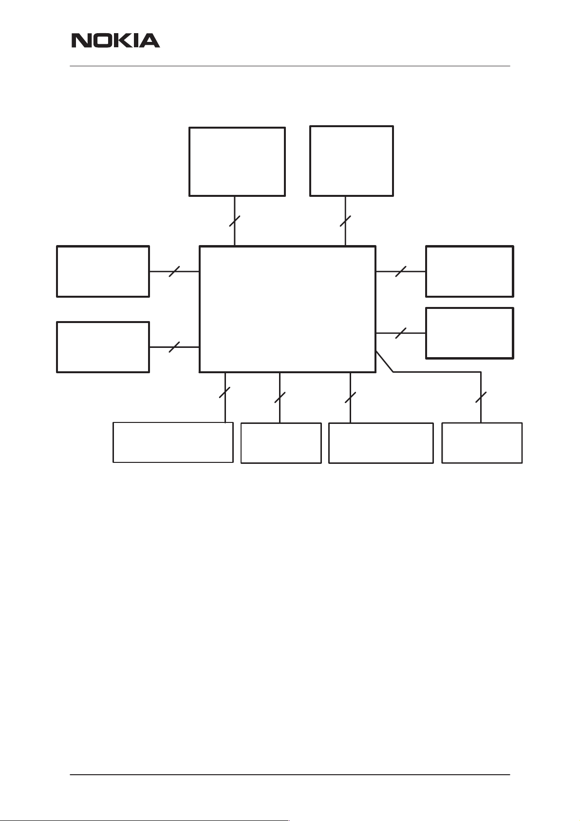
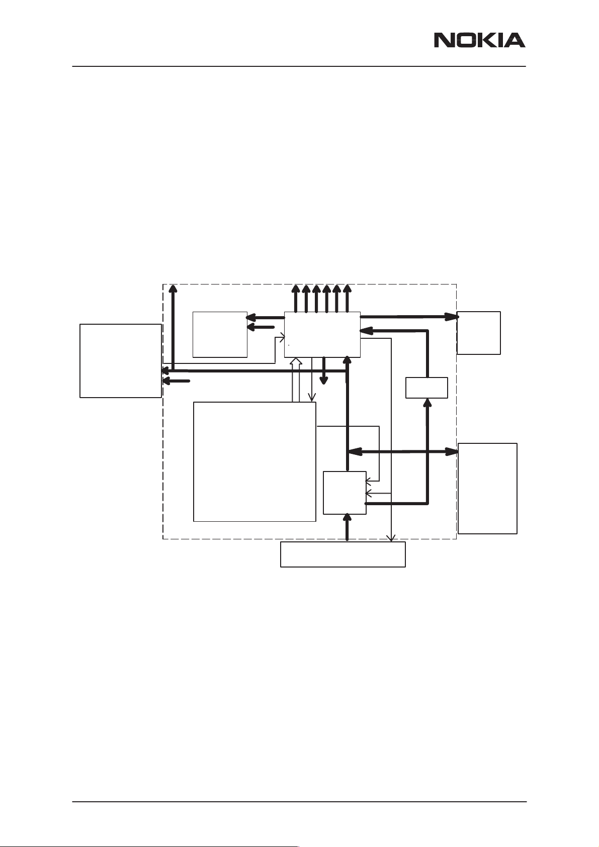
Interconnection Diagram
NSM–3/3D
System Module
Keyboard
module
14
LCD
module
9
64
SIM Battery
Radio
Module
2+2
2
RM7L, RM7LD
Charger
Antenna
2
8
2
4
Mic
IR Link
Earpiece
HF/HS
Issue 4 02/2002
Nokia Corporation
Page 9
NSM–3/3D
System Module
System Module
Baseband Module
The baseband architecture supports a power saving function called ”sleep
mode”. This sleep mode shuts off the VCTCXO, which is used as system
clock source for both RF and baseband. During the sleep mode the sys-
tem runs from a 32 kHz crystal. The phone is waken up by a timer run-
ning from this 32 kHz clock supply. The sleeping time is determined by
some network parameters. The sleep mode is entered when both the
MCU and the DSP are in standby mode and the normal VCTCXO clock
has been switched off.
The battery charging is controlled by a PWM signal from the CCONT. The
PWM duty cycle is determined by a charging software and is fed to the
CHAPS charging switch.
PAMS Technical Documentation
Standard chargers (two wires) provide coarse supply power, which is
switched by the CHAPS for suitable charging voltage and current. Ad-
vanced chargers (three wires) are equipped with a control input. Three
wire chargers are treated like two wire ones.
Block Diagram
TX/RX SIGNALS
UI
IR
COBBA SUPPLY
COBBA
MAD
+
MEMORIES
RF SUPPLIES
CCONT
BB SUPPLY
CHAPS
PA SUPPL Y
32kHz
CLK
SLEEP CLOCK
SIM
VBAT
13MHz
CLK
SYSTEM CLOCK
BATTERY
Page 10
BASEBAND
EXT. AUDIO
HS–connector
Nokia Corporation
Charger
connector
Issue 4 02/2002

PAMS Technical Documentation
Technical Summary
The baseband module consists four ASICs; CHAPS, CCONT, COBBA–
GJP and MAD2WD1, which take care of the baseband functions of the
engine.
The baseband is running from a 2.8V power rail, which is supplied by a
power controlling ASIC CCONT. In the CCONT there are 6 individually
controlled regulator outputs for RF–section and two outputs for the base-
band. In addition there is one +5V power supply output (V5V). The
CCONT contains also a SIM interface, which supports both 3V and 5V
SIM–cards. A real time clock function is integrated into the CCONT, which
utilizes the same 32kHz clock supply as the sleep clock. A backup power
supply is provided for the RTC, which keeps the real time clock running
when the main battery is removed. The backup power supply is a re-
chargable battery. The backup time with the battery is ten minutes mini-
mum.
The interface between the baseband and the RF section is mainly han-
dled by a COBBA ASIC. COBBA provides A/D and D/A conversion of the
in–phase and quadrature receive and transmit signal paths and also A/D
and D/A conversions of received and transmitted audio signals to and
from the user interface. The COBBA supplies the analog TXC and AFC
signals to RF section according to the MAD DSP digital control. Data
transmission between the COBBA and the MAD is implemented using se-
rial bus for high speed signalling and for PCM coded audio signals. Digital
speech processing is handled by the MAD ASIC. COBBA is a dual volt-
age circuit, the digital parts are running from the baseband supply VBB
and the analog parts are running from the analog supply VCOBBA.
NSM–3/3D
System Module
The baseband supports both internal and external microphone inputs and
speaker outputs. Input and output signal source selection and gain control
is done by the COBBA according to control messages from the MAD.
Keypad tones, DTMF, and other audio tones are generated and encoded
by the MAD and transmitted to the COBBA for decoding. A buzzer and an
external vibra alert control signals are generated by the MAD with sepa-
rate PWM outputs.
EMC shieding is implemented using a metallized plastic frame. On the
other side the engine is shielded with PCB grounding. Heat generated by
the circuitry will be conducted out via the PCB ground planes.
Issue 4 02/2002
Nokia Corporation
Page 11

NSM–3/3D
System Module
PAMS Technical Documentation
External and Internal Signals and Connections
This section describes the external electrical connection and interface lev-
els on the baseband. The electrical interface specifications are collected
into tables that covers a connector or a defined interface.
DC (charger) connector
DC (charger) connector is physically integrated in the same component
with the accessory interface connector. DC connector has both jack and
contact pads for desk stand.
Service connector
Name Parameter Min Typ Max Unit Remark
MBUS Serial clock
from the
Prommer
FBUS_RX Serial data
from the
Prommer
FBUS_TX Data ac-
knowledge to
the Prommer
GND GND 0 0 V Ground
0
2.0
0
2.0
0
2.0
logic low
logic low
logic low
logic high
logic low
logic high
0.8
2.85
0.8
2.85
0.5
2.85
V Prommer detection and Seri-
al Clock for synchronous
communication
V Receive Data from
Prommer to Baseband
V Transmit Data from Base-
band to Prommer
The service connector is used as a flash programming interface for updating (i.e. re–programming) the flash program memory and an electrical
access for services to the engine.
When the flash prommer is connected to the phone supply power is provided through the battery contacts and the phone is powered up with a
pulse given to the BTEMP line.
Battery connector
The BSI contact on the battery connector is used to detect when the battery is to be removed to be able to shut down the operations of the SIM
card before the power is lost if the battery is removed with power on. The
BSI contact disconnects earlier than the supply power contacts to give
enough time for the SIM and LCD shut down.
Name Min Typ Max Unit Notes
VBATT 3.0 3.9 4.2 V Battery voltage
BSI
Page 12
0 2.85 V Battery size indication
Phone has 100kohm pull up resistor.
SIM Card removal detection
(Treshold is 2.4V@VBB=2.8V)
67 68 69 kohm Battery indication resistor (BLB–2)
0 0 1 kohm Battery indication resistor (service battery)
Nokia Corporation
Issue 4 02/2002
PAMS Technical Documentation
NSM–3/3D
System Module
NotesUnitMaxTypMinName
BTEMP
BGND 0 0 V Battery ground
0 1.4 V Battery temperature indication
Phone has a 100k (+–5%) pullup resistor,
Battery package has a NTC pulldown resistor:
47k+–5%@+25C , B=4050+–3%
2.1
5 10
1.9
90 100
0 1 kohm Local mode initialization (in production)
3
20
2.85
200
V
ms
V
ms
Phone power up by battery (input)
Power up pulse width
Battery power up by phone (output)
Power up pulse width
SIM card connector
The SIM card connector is located on the engine board beside the battery
pack.
Pin Name Parameter Min Typ Max Unit Notes
4 GND GND 0 0 V Ground
3, 5 VSIM 5V SIM Card
3V SIM Card
6 DATA 5V Vin/Vout
3V Vin/Vout
2 SIMRST 5V SIM Card
3V SIM Card
4.8
2.8
4.0
0
2.8
0
4.0
2.8
5.0
3.0
”1”
”0”
”1”
”0”
”1”
”1”
5.2
3.2
VSIM
0.5
VSIM
0.5
VSIM
VSIM
V Supply voltage
V SIM data
Trise/Tfall max 1us
V SIM reset
1 SIMCLK Frequency
Trise/Tfall
3.25
25
MHz
ns
SIM clock
RTC backup battery
The RTC block in CCONT needs a power backup to keep the clock running when the phone battery is disconnected. The backup power is supplied from a rechargable polyacene battery that can keep the clock running ten minutes minimum. The backup battery is charged from the main
battery through CHAPS.
Signal Parameter Min Typ Max Unit Notes
VBACK
VBACK
Backup battery charging from CHAPS
Backup battery charging from CHAPS
Backup battery supply
to CCONT
Backup battery supply
to CCONT
3.02 3.15 3.28 V
100 200 500 uA Vout@VBAT–0.2V
2 3.28 V
80 uA
Issue 4 02/2002
Nokia Corporation
Page 13
NSM–3/3D
System Module
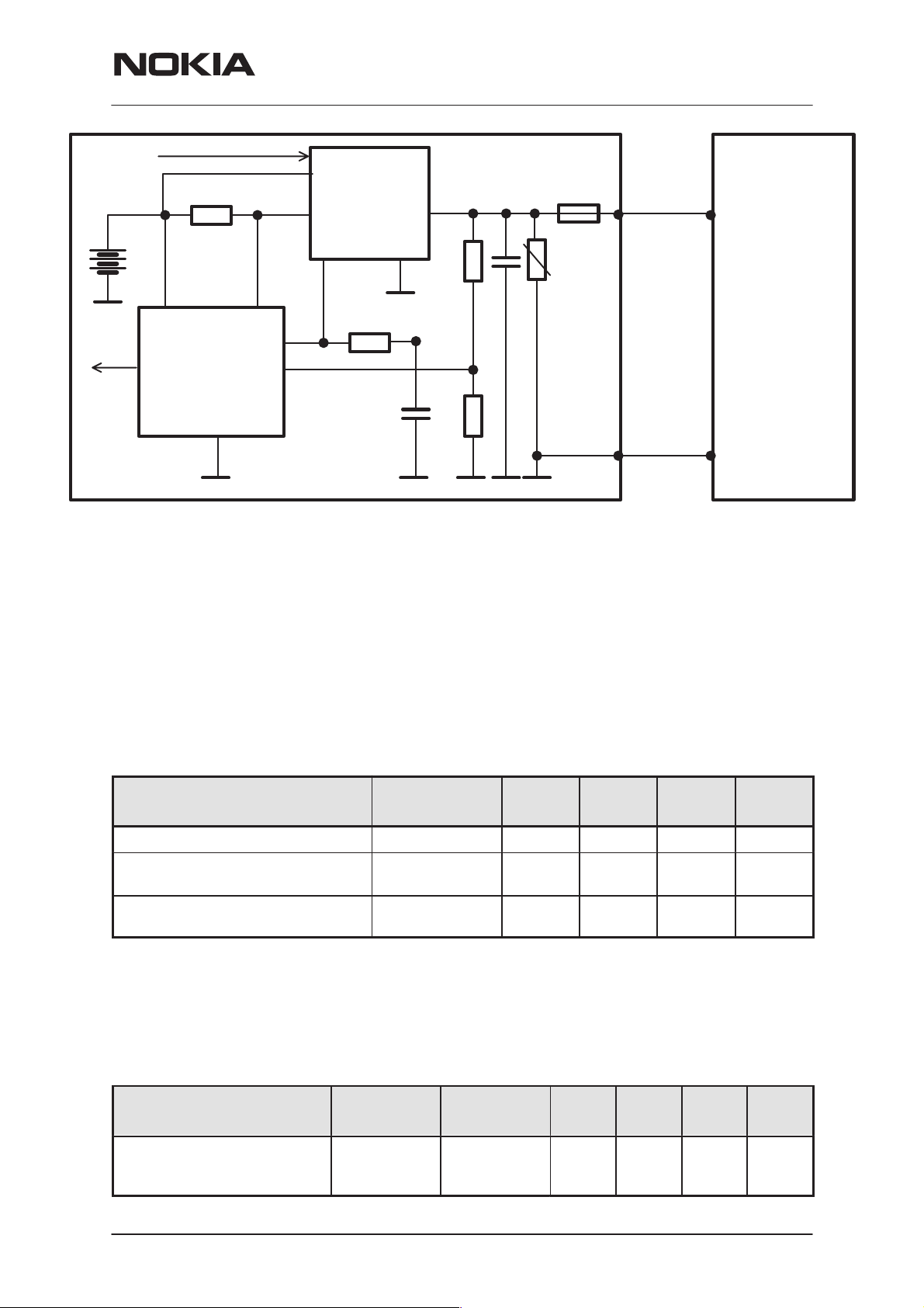
Power Distribution
In normal operation the baseband is powered from the phone‘s battery.
The battery consists of one Lithium–Ion cell. An external charger can be
used for recharging the battery and supplying power to the phone.
The baseband contains parts that control power distribution to whole
phone excluding those parts that use continuous battery supply. The battery feeds power directly to the CCONT and UI (buzzer and display and
keyboard lights).
The power management circuit CHAPS provides protection against overvoltages, charger failures and pirate chargers etc. that would otherwise
cause damage to the phone.
PAMS Technical Documentation
PA SUPPL Y
VCOBBA
COBBA
UI
VBAT
VBB
BASEBAND
VBB
MAD
+
MEMORIES
RF SUPPLIES
CCONT
PWRONX
CNTVR
CHARGER CONNECTOR
PWM
VBB
PURX
LIM
CHAPS
VIN
VSIM
SIM
RTC
BACKUP
VBAT
BATTERY
Battery charging
The electrical specifications give the idle voltages produced by the acceptable chargers at the DC connector input. The absolute maximum input voltage is 30V due to the transient suppressor that is protecting the
charger input. At phone end there is no difference between a plug–in
charger or a desktop charger. The DC–jack pins and bottom connector
charging pads are connected together inside the phone.
Page 14
Nokia Corporation
Issue 4 02/2002
PAMS Technical Documentation
NSM–3/3D
System Module
MAD
VBAT
MAD
CCONTINT
CCONT
Startup Charging
LIM
0R22
PWM_OUT
GND
ICHAR
VCHAR
VOUT
CHAPS
RSENSE
PWM
22k
VCH
GND
1n
TRANSCEIVER
1u
100k
10k
30V
2A
VIN
L_GND
CHARGER
When a charger is connected, the CHAPS is supplying a startup current
minimum of 130mA to the phone. The startup current provides initial
charging to a phone with an empty battery. Startup circuit charges the
battery until the battery voltage level is reaches 3.0V (+/– 0.1V) and the
CCONT releases the PURX reset signal and program execution starts.
Charging mode is changed from startup charging to PWM charging that is
controlled by the MCU software. If the battery voltage reaches 3.55V
(3.75V maximum) before the program has taken control over the charging, the startup current is switched off. The startup current is switched on
again when the battery voltage is sunken 100mV (nominal).
Parameter Symbol Min Typ Max Unit
VOUT Start– up mode cutoff limit Vstart 3.45 3.55 3.75 V
VOUT Start– up mode hysteresis
NOTE: Cout = 4.7 uF
Start–up regulator output current
VOUT = 0V ... Vstart
Vstarthys 80 100 200 mV
Istart 130 165 200 mA
Battery Overvoltage Protection
Output overvoltage protection is used to protect phone from damage.
This function is also used to define the protection cutoff voltage for different battery types (Li or Ni). The power switch is immediately turned OFF if
the voltage in VOUT rises above the selected limit VLIM1 or VLIM2.
Parameter Symbol LIM input Min Typ Max Unit
Output voltage cutoff limit
(during transmission or Li–
battery)
VLIM LOW 4.4 4.6 4.8 V
Issue 4 02/2002
Nokia Corporation
Page 15
NSM–3/3D
System Module
The voltage limit (VLIM1 or VLIM2) is selected by logic LOW or logic
HIGH on the CHAPS (N101) VLIM input pin. In NSM–3 phones VLIM is
fixed low in HW.
When the switch in output overvoltage situation has once turned OFF, it
stays OFF until the the battery voltage falls below VLIM and PWM = LOW
is detected. The switch can be turned on again by setting PWM = HIGH.
VCH
VCH<VOUT
VOUT
PAMS Technical Documentation
t
VLIM
SWITCH
PWM (1 Hz)
ON OFF
t
ON
Page 16
Nokia Corporation
Issue 4 02/2002
PAMS Technical Documentation
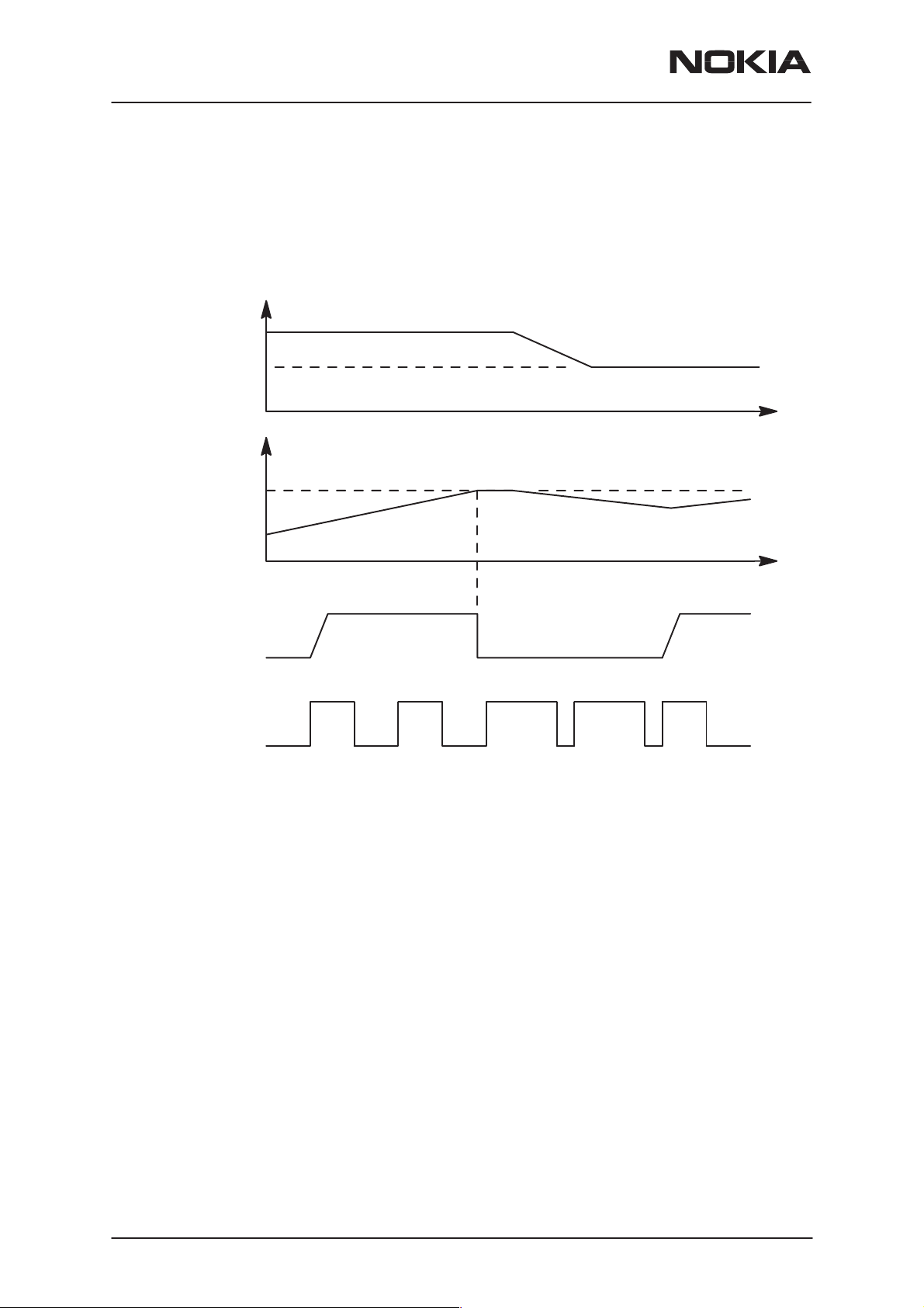
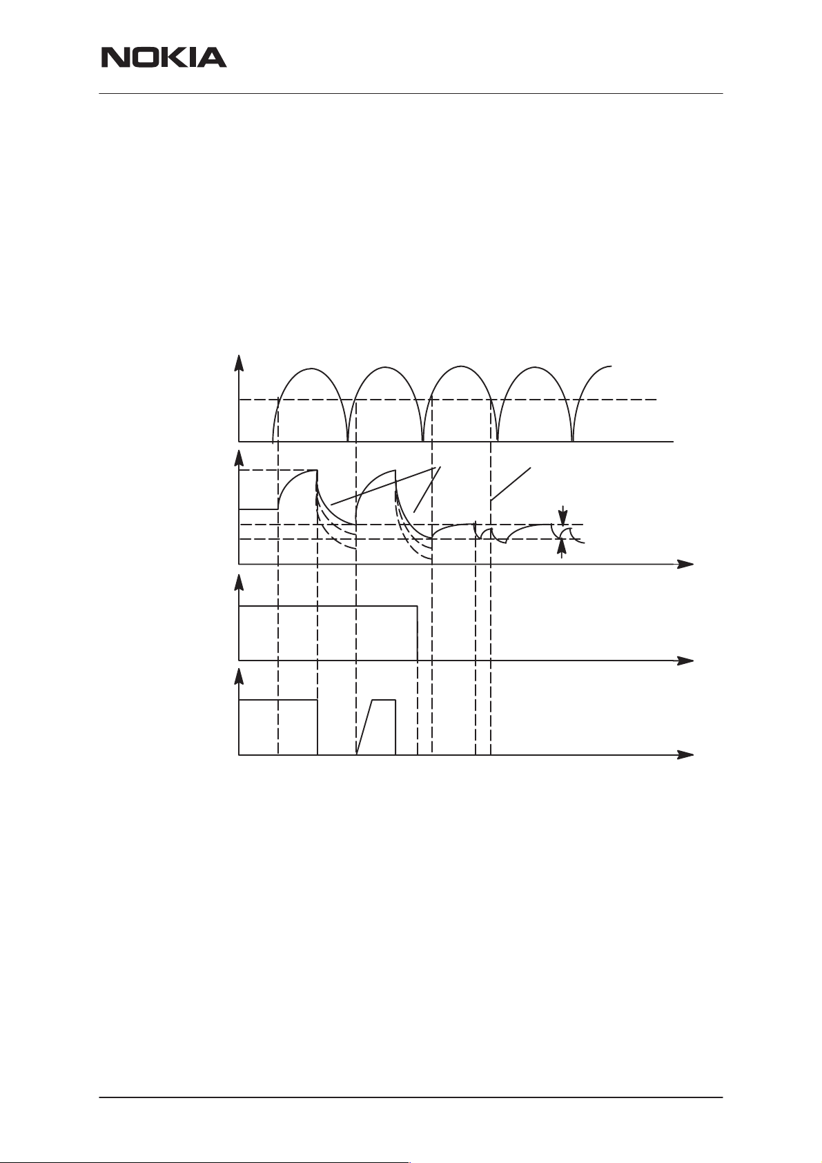
Battery Removal During Charging
Output overvoltage protection is also needed in case the main battery is
removed when charger connected or charger is connected before the battery is connected to the phone.
With a charger connected, if VOUT exceeds VLIM, CHAPS turns switch
OFF until the charger input has sunken below Vpor (nominal 3.0V, maximum 3.4V). MCU software will stop the charging (turn off PWM) when it
detects that battery has been removed. The CHAPS remains in protection
state as long as PWM stays HIGH after the output overvoltage situation
has occured.
NSM–3/3D
System Module
VCH
(Standard
Charger)
VOUT
PWM
SWITCH
Vpor
VLIM
4V
Vstart
”1”
”0”
ON
OFF
Droop depends on load
& C in phone
2
5
4
6
7
Istart off due to VCH<Vpor
Vstarthys
t
t
t
1.1Battery removed, (standard) charger connected, VOUT rises (follows charger voltage)
2. VOUT exceeds limit VLIM(X), switch is turned immediately OFF
3.3VOUT falls (because no battery) , also VCH<Vpor (standard chargers full–rectified
output). When VCH > Vpor and VOUT < VLIM(X) –> switch turned on again (also PWM
is still HIGH) and VOUT again exceeds VLIM(X).
4. Software sets PWM = LOW –> CHAPS does not enter PWM mode
5. PWM low –> Startup mode, startup current flows until Vstart limit reached
6. VOUT exceeds limit Vstart, Istart is turned off
7. VCH falls below Vpor
Issue 4 02/2002
Nokia Corporation
Page 17
NSM–3/3D
System Module
PAMS Technical Documentation
PWM
When a charger is used, the power switch is turned ON and OFF by the
PWM input. PWM rate is 1Hz. When PWM is HIGH, the switch is ON and
the output current Iout = charger current – CHAPS supply current. When
PWM is LOW, the switch is OFF and the output current Iout = 0. To prevent the switching transients inducing noise in audio circuitry of the phone
soft switching is used.
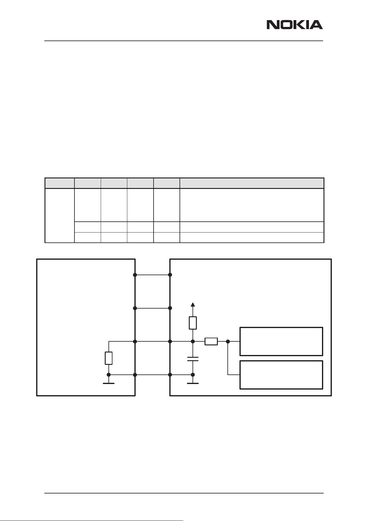
Battery Identification
Different battery types are identified by a pulldown resistor inside the battery pack. The BSI line inside transceiver has a 100k pullup to VBB. The
MCU can identify the battery by reading the BSI line DC–voltage level
with a CCONT (N100) A/D–converter.
Name Min Typ Max Unit Notes
BSI
0 2.8 V Battery size indication
100k pullup resistor to VBB in phone
SIM Card removal detection
(Treshold is 2.4V@VBB=2.8V)
67 68 69 kohm Indication of a BLB–2 battery (650 mAh Li–Ion)
0 1 kohm Indication resistor for a service battery
VBATT
BATTERY
BTEMP
BSI
R
s
BGND
2.8V
100k
10n
10k
TRANSCEIVER
BSI
SIMCardDetX
CCONT
MAD
Page 18
The battery identification line is used also for battery removal detection.
The BSI line is connected to a SIMCardDetX line of MAD2. SIMCardDetX
is a threshold detector with a nominal input switching level 0.85xVcc for a
rising edge and 0.55xVcc for a falling edge. The battery removal detection
is used as a trigger to power down the SIM card before the power is lost.
The BSI contact in the battery contact disconnects before the other contacts so that there is a delay between battery removal detection and supply power off.
Nokia Corporation
Issue 4 02/2002
 Loading...