

Page 1

PAMS T echnical Documentation
NSB-8 Series Transceivers
T roubleshooting Instructions
Issue 1 01/02 ãNokia Corporation
Page 2

NSB-8
Troub l esh oot ing Instructions PAMS Technical Document a t ion
Table of Contents
Page No
Transceiver Troubleshooting ......................................................................................... 5
Baseband Troubleshooting ..........................................................................................5
PWB Points (and Measurement Points).................................................................... 5
Troubleshooting steps ................................................................................................34
General instructions................................................................................................. 35
RF Troubleshooting ...................................................................................................55
Phone Settings for TX Troubleshooting.................................................................. 55
Phone Settings for RX Troubleshhoting ................................................................. 55
NO TX GSM 1900.................................................................................................. 56
NO RX GSM 1900.................................................................................................. 56
Measurements points for AMS and production repair ..............................................57
TX Troubleshooting points ..................................................................................... 57
RX Troubleshooting points..................................................................................... 63
RF Tuning and Calibration Instructions....................................................................... 67
TX tunings .................................................................................................................67
TX Output power tuning ............................................................................................67
TX IQ tuning ..............................................................................................................70
RX tunings .................................................................................................................72
Channel select filter calibration .................................................................................73
RX tuning GSM1900 .................................................................................................74
AM suppression tuning ..............................................................................................76
RF Service Tools.......................................................................................................... 78
MJS-46 Module Jig ....................................................................................................78
JVB-1 Docking Station, MJF-6 Adapter and coupler CPL-6 ....................................78
Coupler attenuation calibration ..................................................................................78
Functionality Testing Limits .....................................................................................78
JXS-1 Shield Box ......................................................................................................79
Page 2 ãNokia Corporation Issue 1 01/02
Page 3

NSB-8
PAMS Technical Documentation Troubleshooting Instructions
List of Figures
Page No
Fig 1 Picture of top testpoints..............................................................................................5
Fig 2 Picture of bottom testpoints........................................................................................6
Fig 3 Top testpoints .............................................................................................................7
Fig 4 Bottom testpoints........................................................................................................8
Fig 5 C660: RFCLK (26 MHz), VCTCXO (G660 pin 3) -> HAGAR (N600 pin H1).......14
Fig 6 J1: RESET, UPP (D400 pin D12) -> HAGAR (N600 pin E3) ..................................14
Fig 7 J2: RFBUSDA, UPP (D400 pin F12) -> HAGAR (N600 pin E1).............................15
Fig 8 J3: RFBUSCLK, UPP (D400 pin G11) -> HAGAR (N600 pin E2)..........................15
Fig 9 J3: RFBUSCLK (closer look), UPP (D400 pin G11) -> HAGAR (N600 pin E2).....16
Fig 10 J4: RFBUSEN1, UPP (D400 pin G13) -> HAGAR (N600 pin D1) ........................16
Fig 11 J386: SIMDATA, UEM (D200 pin B2) <-> SIM CARD READER (X386 pin 4...17
Fig 12 J387: SIMRST, UEM (D200 pin A2) <-> SIM CARD READER (X386 pin 2).....17
Fig 13 J388: SIMCLK, UEM (D200 pin B3) <-> SIM CARD READER (X386 pin 3) ....18
Fig 14 J396 PAD 2: FBUSTX (during flashing), UEM (D200 pin N5) -> SERVICE INTER-
FACE (J396 PAD 2)..............................................................................................................18
Fig 15 J396 PAD 3 FBUSRX (during flashing), SERVICE INTERFACE (J396 PAD 3) ->
UEM (D200 pin P5)...............................................................................................................19
Fig 16 J396 PAD 7: MBUS (during flashing), UEM (D200 pin M6) <-> SERVICE INTER-
FACE (J396 PAD 7)..............................................................................................................19
Fig 17 J402: PURX, UEM (D200 pin C10) -> UPP (D400 pin K2)...................................20
Fig 18 J403: SLEEPX, UEM (D200 pin B11) -> UPP (D400 pin L1)................................20
Fig 19 J404: SLEEPCLK, UEM (D200 pin D9) -> UPP (D400 pin H3)............................21
Fig 20 J405: UEMINT, UEM (D200 pin A10) -> UPP (D400 pin J2) ...............................21
Fig 21 J406: CBUSCLK, UEM (D200 pin A8) -> UPP (D400 pin G1).............................22
Fig 22 J407: CBUSDA, UEM (D200 pin B7) <-> UPP (D400 pin G2) .............................22
Fig 23 J408: CBUSENX, UEM (D200 pin C8) -> UPP (D400 pin F3)..............................23
Fig 24 J409: MBUSTX (during flashing), UPP (D400 pin E3) -> UEM (D200 pin C6)....23
Fig 25 J410: MBUSRX (during flashing), UEM (D200 pin D6) -> UPP (D400 pin D3)...24
Fig 26 J411: FBUSTX (during flashing), UPP (D400 pin F1) -> UEM (D200 pin A7).....24
Fig 27 J412: FBUSRX (during flashing), UEM (D200 pin C7) -> UPP (D400 pin E4).....25
Fig 28 J413: DBUSCLK, UEM (D200 pin D10) -> UPP (D400 pin K3)...........................25
Fig 29 J414: DBUSDA, UEM (D200 pin A11) <-> UPP (D400 pin L3) ...........................26
Fig 30 J415: DBUSENX1, UEM (D200 pin B10) -> UPP (D400 pin J3)..........................26
Fig 31 J416: EXTWRX (during flashing), UPP (D400 pin N9) -> FLASH (D450 pin A6)27
Fig 32 J417: EXTRDX, UPP (D400 pin L7) -> FLASH (D450 pin C10)..........................27
Fig 33 J419: FLSCLK, UPP (D400 pin N12) -> FLASH (D450 pin A4)...........................28
Fig 34 J420: FLSCSX, UPP (D400 pin N6) -> FLASH (D450 pin B9) .............................28
Fig 35 J700: TXP, UPP (D400 pin D11) -> HAGAR (N600 pin D5).................................29
Fig 36 R301: PWRONX, POWER BUTTON (S300) -> UEM (D200 pin P7)...................29
Fig 37 R305: KLIGHT, UEM (D200 pin F3) -> BACKLIGHT CIRCUITRY (V300 pins 2,3,5
and V301 pins 2,5,6) .............................................................................................................30
Fig 38 R420: RFCLK (13 MHz), HAGAR (N600 pin E4) -> UPP (D400 pin M5)...........30
Fig 39 X100 PIN 9: VIBRA, UEM (D200 pin G3) -> SYSTEM CONNECTOR (X100 pin 9)
31
Fig 40 X300 PIN 1: XRES (startup), UPP (D400 pin A7) -> LCD CONNECTOR (X300 pin
1)............................................................................................................................................31
Issue 1 01/02 ãNokia Corporation Page 3
Page 4
NSB-8
Troub l esh oot ing Instructions PAMS Technical Document a t ion
Fig 41 X300 PIN 2: XCS, UPP (D400 pin C7) -> LCD CONNECTOR (X300 pin 2).......32
Fig 42 X300 PIN 4: SDA, UPP (D400 pin B6) -> LCD CONNECTOR (X300 pin 4) ......32
Fig 43 X300 PIN 5: SCLK, UPP (D400 pin C6) -> LCD CONNECTOR (X300 pin 5)....33
Fig 44 X300 PIN 8: VOUT, LCD CONNECTOR (X300 PIN 8) -> C301 and C302 ........33
Fig 45 X303 PIN 2: KEYB_LIGHT, BACKLIGHT CIRCUITRY (V300 pin 6) -> UI CON-
NECTOR (X303 pin 2)..........................................................................................................34
Fig 46 Troubleshooting: Top...............................................................................................36
Fig 47 Phone is dead............................................................................................................38
Fig 48 Flash Faults...............................................................................................................39
Fig 49 Phone is jammed.......................................................................................................41
Fig 50 Charging Faults ........................................................................................................43
Fig 51 SIM Card ..................................................................................................................44
Fig 52 Audio Faults ............................................................................................................45
Fig 53 Display faults............................................................................................................49
Fig 54 Keypad Faults...........................................................................................................52
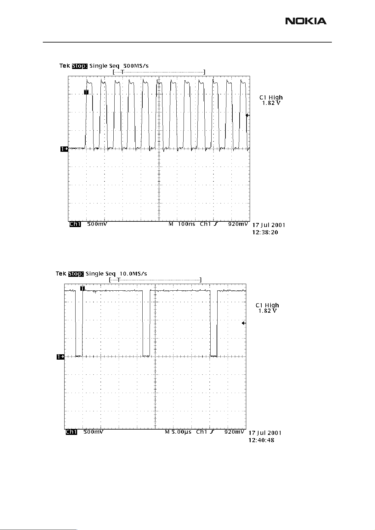
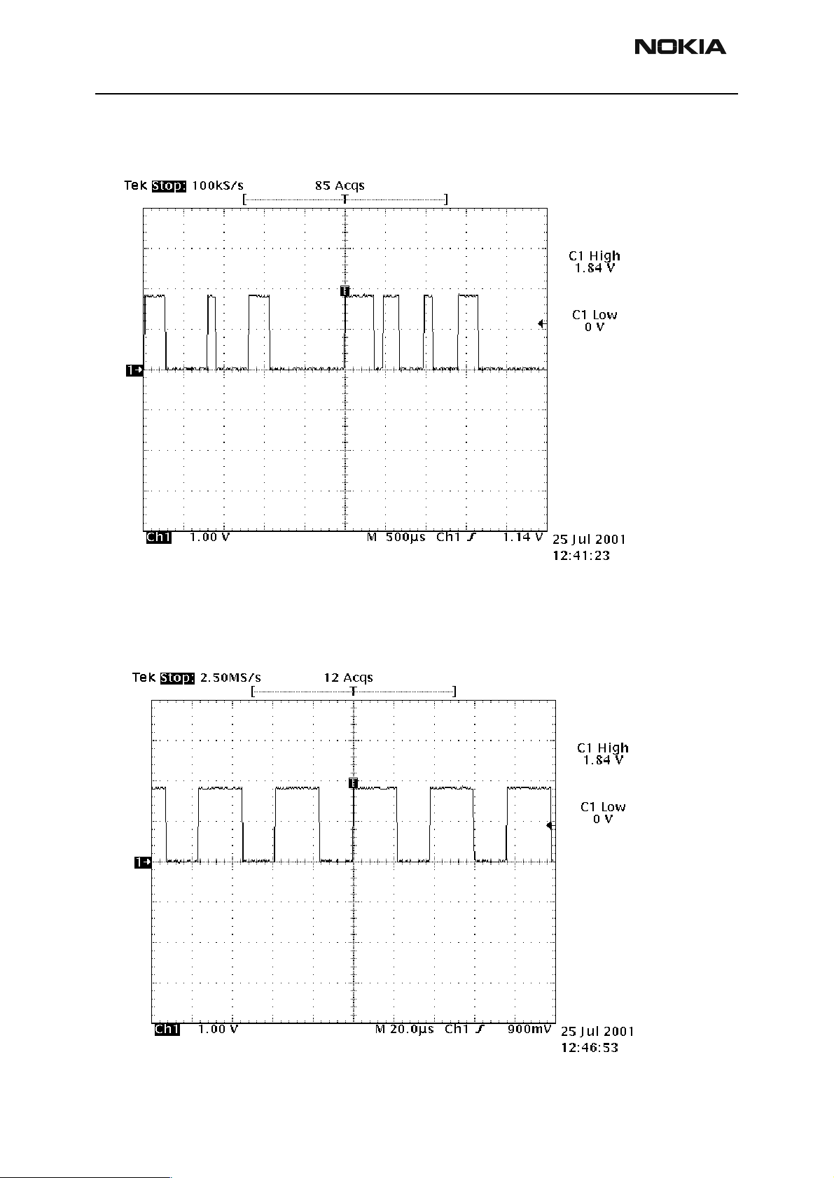
Fig 55 TP 20 ........................................................................................................................57
Fig 56 TP 21 ........................................................................................................................57
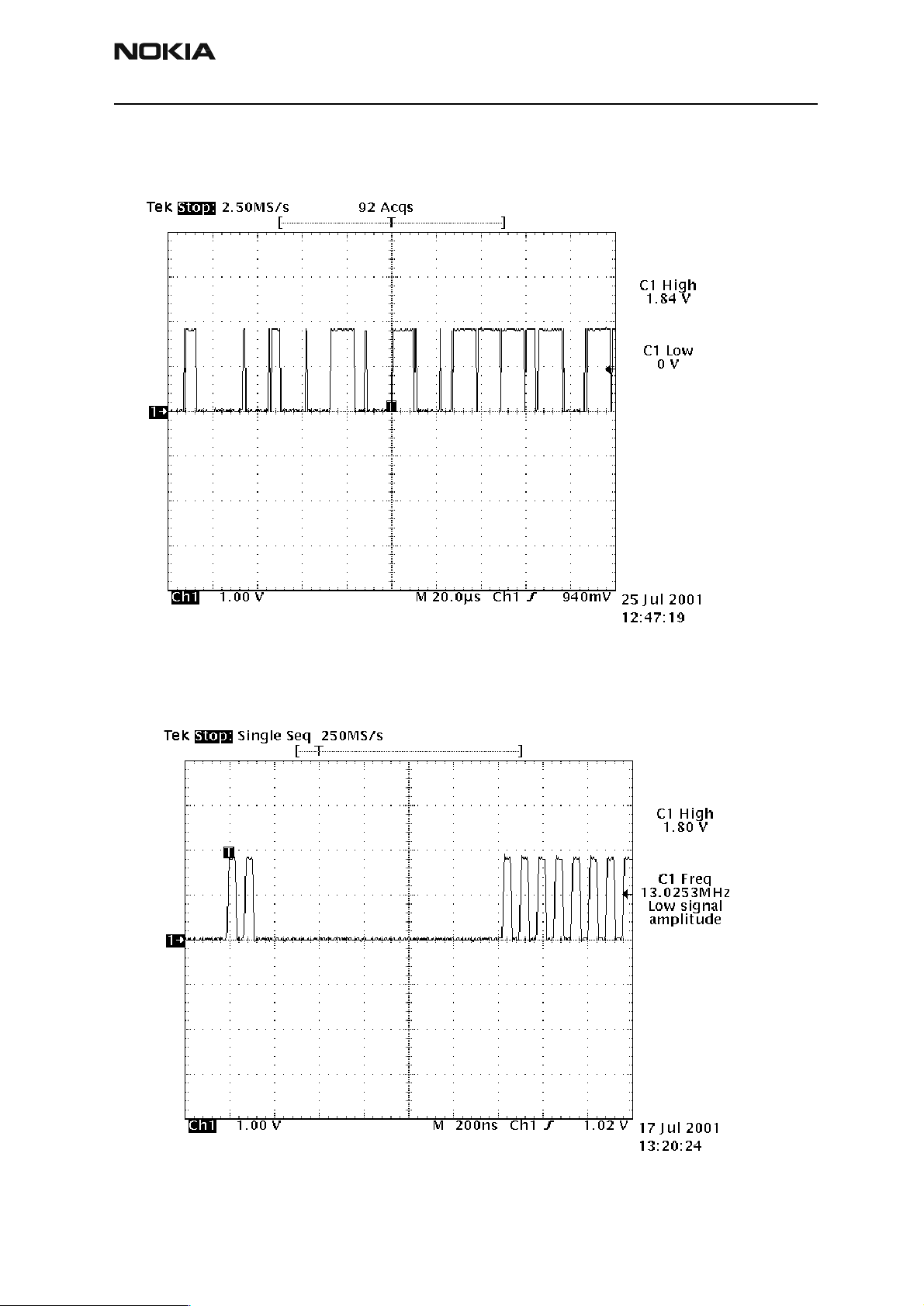
Fig 57 TP 22 ........................................................................................................................58
Fig 58 TP 51, 52, 53 ............................................................................................................58
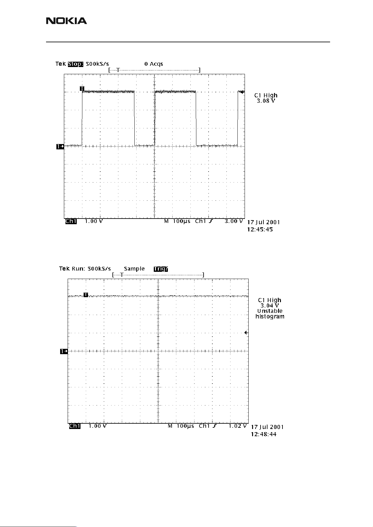
Fig 59 TP 23, 24 ..................................................................................................................59
Fig 60 TP 40 ........................................................................................................................59
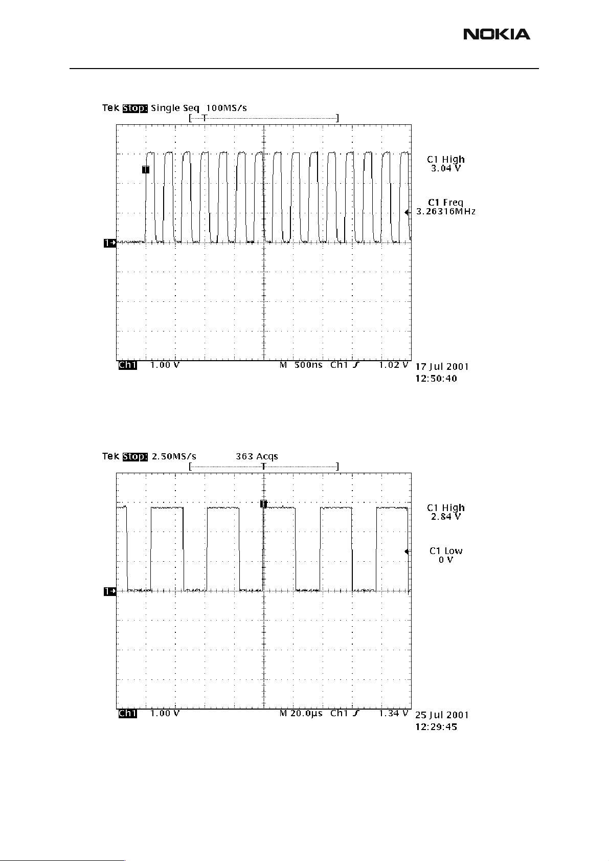
Fig 61 TP 25, 28 ..................................................................................................................60
Fig 62 TP 26, 27 ..................................................................................................................60
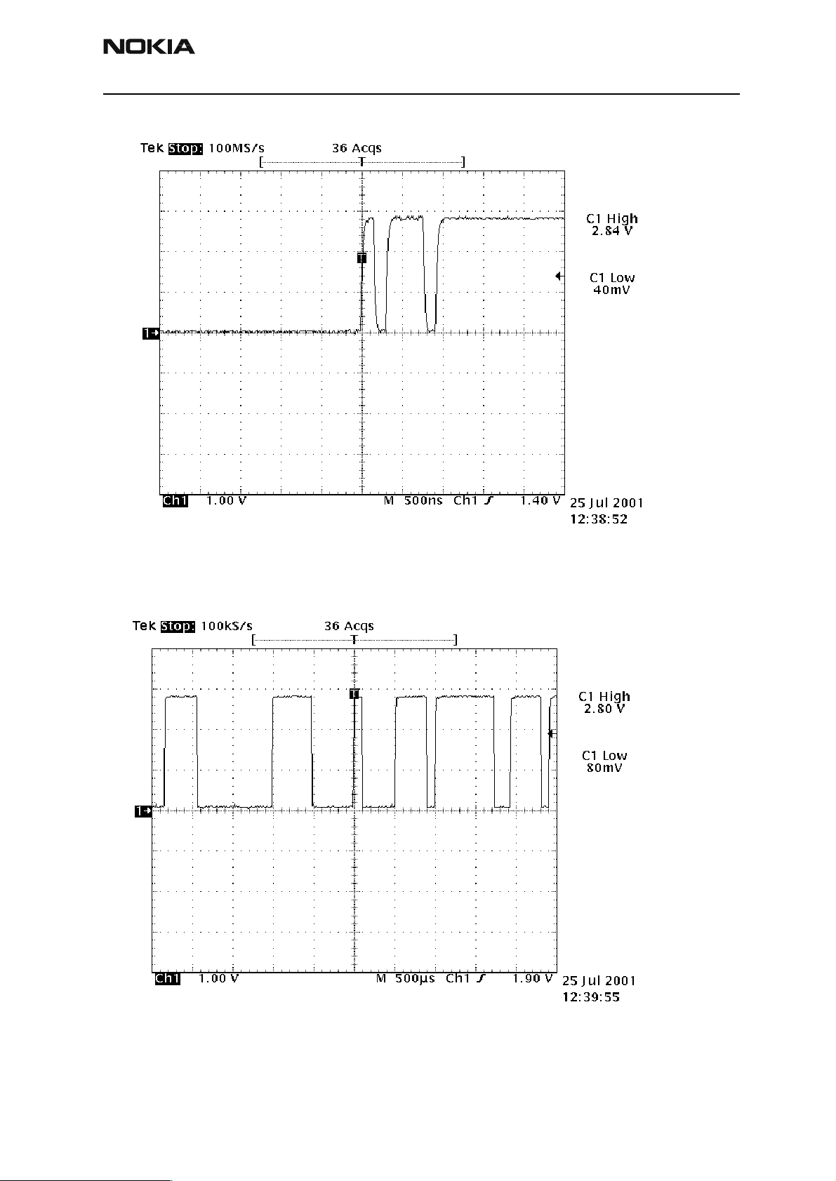
Fig 63 TP 30 ........................................................................................................................61
Fig 64 TP 29 ........................................................................................................................61
Fig 65 TP 20 ........................................................................................................................62
Fig 66 TP 20 ........................................................................................................................63
Fig 67 TP 31, 32 ..................................................................................................................63
Fig 68 TP 33 ........................................................................................................................64
Fig 69 TP 36 ........................................................................................................................64
Fig 70 TP 37 (RX continuous mode)...................................................................................65
Fig 71 TP 37 (RX burst mode) ...........................................................................................65
Fig 72 TP 51, 52, 53 ............................................................................................................66
Fig 73 TP 40 ........................................................................................................................66
Fig 74 Power 30 dBm..........................................................................................................80
Fig 75 Phase error RMS.......................................................................................................80
Fig 76 Signal Strength Reading...........................................................................................81
Fig 77 BER(-102 dBm)........................................................................................................81
Page 4 ãNokia Corporation Issue 1 01/02
Page 5
NSB-8
PAMS Technical Documentation Troubleshooting Instructions
Transceiver T roubleshooting
Baseband Troubleshooting
PWB Points (and Measurement Points)
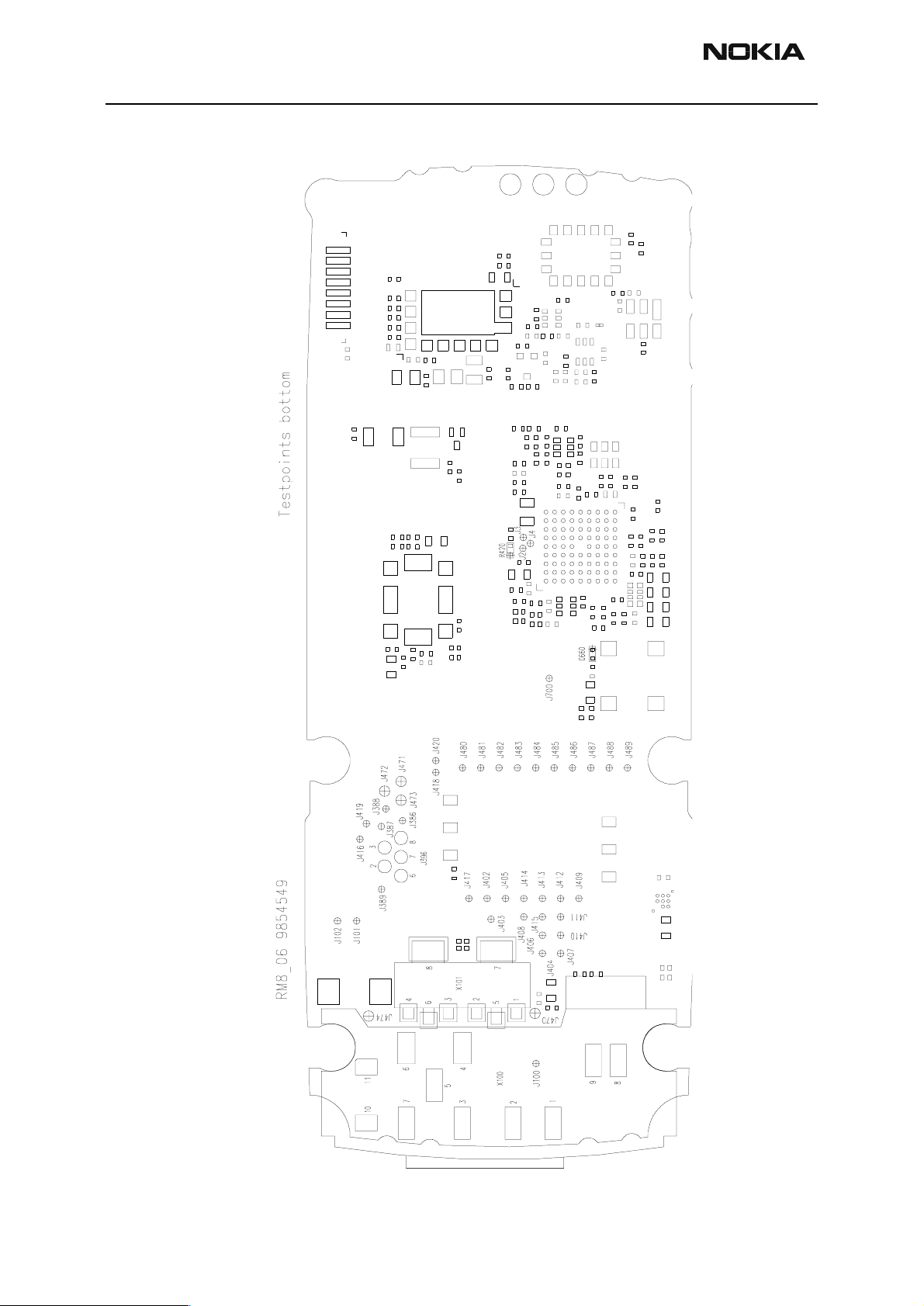
The following figures are the most needed testpoints in the NSB-8 transceiver.
Figure 1: Picture of top testpoints
Issue 1 01/02 ãNokia Corporation Page 5
Page 6
NSB-8
Troub l esh oot ing Instructions PAMS Technical Document a t ion
Figure 2: Picture of bottom testpoints
Page 6 ãNokia Corporation Issue 1 01/02
Page 7
NSB-8
PAMS Technical Documentation Troubleshooting Instructions
Figure 3: Top testpoints
Issue 1 01/02 ãNokia Corporation Page 7
Page 8
NSB-8
Troub l esh oot ing Instructions PAMS Technical Document a t ion
Figure 4: Bottom testpoints
Page 8 ãNokia Corporation Issue 1 01/02
Page 9
NSB-8
PAMS Technical Documentation Troubleshooting Instructions
Table 1: Testpoints
REFERENCE SIGNAL NOTE
C205 VFLASH1 2.78 V regulator output
UEM (D200) -> external FLASH memory
C206 VANA 2.78 V regulator output
UEM (D200) -> internal and external analog circuitry
C207 VIO 1.8 V regulator output
UEM (D200) -> internal and external logic circuitry
C208 VCORE 1.8 V programmable regulator output
UEM (D200) -> UPP (D400)
C221 VR1A 4.75 V RF regulator output
UEM (D200) -> HAGAR (N600)
C222 VR4 2.78 V regulator output
UEM (D200) -> HAGAR (N600)
C223 VR6 2.78 V regulator output
UEM (D200) -> HAGAR (N600)
C224 VR7 2.78 V regulator output
UEM (D200) -> VCO (G650)
C225 VR2 2.78 V regulator output
UEM (D200) -> transf balun (T700)
C227 VR3 2.78 V regulator output
UEM (D200) -> HAGAR (N600) and VCTCXO (G660)
C660 RFCLK (26MHz) Main clock oscillator 26 MHz, see Figure 5, “C660: RFCLK (26 MHz ),
VCTCXO (G660 pin 3) -> HAGAR (N600 pin H1),” on page 14
VCTCXO (G660) -> HAGAR (N600)
J1 RESET Reset signal, see Fi gure 6, “J1: RESET, UPP (D400 pin D12) -> HAGAR
(N600 pin E3),” on pa ge 14
UPP (D400) -> HAGAR (N600)
J2 RFBUSDA RFBUS data, see Figure 7, “J2: RFBUSDA, UPP (D400 pin F12) -> HAGAR
(N600 pin E1),” on pa ge 15
UPP (D400) -> HAGAR (N600)
J3 RFBUSCLK RFBUS clock, see Figure 8, “J3: RFBUSCLK, UPP (D4 00 p in G 11) ->
HAGAR (N600 pin E2),” on page 15 and Figure 9, “J3: RFBUSCLK (closer
look), UPP (D400 pi n G 11) -> HAGAR (N600 pin E2),” on page 16
UPP (D400) -> HAGAR (N600)
J4 RFBUSEN1 RFBUS enable, see Figure 10, “J4: RFBUSEN1, UPP (D400 pin G13) ->
HAGAR (N600 pin D1 ), ” on page 16
UPP (D400) -> HAGAR (N600)
J100 VBAT Battery voltage pad for jig
J101 BSI Battery size indicator for jig
J102 BTEMP Battery temperature for jig
Issue 1 01/02 ãNokia Corporation Page 9
Page 10
NSB-8
Troub l esh oot ing Instructions PAMS Technical Document a t ion
J386 SIMDATA SIM data, see Figure 11, “J386: SIMDAT A, UEM (D200 pin B2) <-> SIM CARD
READER (X386 pin 4,” on page 17
UEM (D200) <-> SIM CARD READER (X386)
J387 SIMRST SIM reset, see Figure 12, “J387: SIMRST, UEM (D200 pin A2) <-> SIM
CARD READER (X386 pin 2) ,” on page 17
UEM (D200) -> SIM CARD READER (X386)
J388 SIMCLK SIM clock, see Figure 13, “J388: SIMCLK, UEM (D200 pin B3) <-> SIM
CARD READER (X386 pin 3) ,” on page 18
UEM (D200) -> SIM CARD READER (X386)
J389 VSIM SIM voltage 3 V or 1.8 V
UEM (D200) -> SIM CARD READER (X386)
J396 PAD 2 FBUSTX FBUS transmitted data, see Figure 14, “J396 PAD 2: FBUSTX (during
flashing), UEM (D200 pin N5 ) -> SERV ICE INTERFACE (J396 PAD 2),”
on page 18 (during flashing)
UEM (D200) -> SERVICE INTERFACE
J396 PAD 3 FBUSRX FBUS received data, s ee Figure 15, “J396 PAD 3 FBUSRX (duri ng f lash-
ing), SERVICE INTERFACE (J396 PAD 3) -> UEM (D200 pin P5),” on
page 19 (during flashing)
SERVICE INTERFACE -> UEM (D200)
J396 PAD 6 VPP Flash programming voltage
UEM (D200), SERVICE INTERFACE -> FLASH (D450)
J396 PAD 7 MBUS One wire bidirectional serial bus, see Figure 16, “J396 PAD 7: MBUS (dur-
ing flashing), UEM (D200 pin M6) <-> SERV ICE INTERFACE (J396 PAD
7),” on page 19 (dur i ng fl ashing)
UEM (D200) <-> SERVICE INTERFACE
J396 PAD 8 GND Ground p oint for s ervice interface
J402 PURX Power Up Reset, see Fi gure 17, “J402: PURX, UEM (D200 pin C10) ->
UPP (D400 pin K2),” on page 20
UEM (D200) -> UPP (D400)
J403 SLEEPX Sleep enable, see Figure 18, “J403: SLEEPX, UEM (D200 pin B11) -> UPP
(D400 pin L1),” on pa ge 20
UEM (D200) -> UPP (D400)
J404 SLEEPCLK Sleep clock, see Figure 19, “J404: SLEEPCLK, UEM (D200 pin D9) -> UPP
(D400 pin H3),” on page 21
UEM (D200) -> UPP (D400)
J405 UEMINT UEM interrupt, see Figure 20, “J405: UEMINT, UEM (D200 pin A10) ->
UPP (D400 pin J2),” on page 21
UEM (D200) -> UPP (D400)
J406 CBUSCLK CBUS clock, see Figure 21, “J406: CBUSCLK, UEM (D200 pin A8) -> UPP
(D400 pin G1),” on page 22
UEM (D200) -> UPP (D400)
J407 CBUSDA CBUS data, see Figure 22, “J407: CBUSDA, UEM (D200 pin B7) <-> UPP
(D400 pin G2),” on page 22
UEM (D200) <-> UPP (D400)
Page 10 ãNokia Corporation Issue 1 01/02
Page 11
NSB-8
PAMS Technical Documentation Troubleshooting Instructions
J408 CBUSENX CBUS enable, see Figure 23, “J408: CBUSENX, UEM (D200 pin C8) ->
UPP (D400 pin F3),” on page 23
UEM (D200) -> UPP (D400)
J409 MBUSTX MBUS transmitted data, see Figure 24, “J409: MBUSTX (during flashing),
UPP (D400 pin E3) -> UEM (D20 0 pi n C6) ,” o n page 23 (during flashing)
UPP (D400) -> UEM (D200)
J410 MBUSRX MBUS received data, see Figure 25, “J410: MBUSRX (during flashing),
UEM (D200 pin D6) -> UPP (D400 pin D3),” on page 24 (during flashing)
UEM (D200) -> UPP (D400)
J411 FBUSTX FBUS transmitted data, see Figure 26, “J411: FBUSTX (during flashing),
UPP (D400 pin F1) -> UEM (D200 pin A7),” on pag e 24 (during flashing)
UPP (D400) -> UEM (D200)
J412 FBUSRX FBUS received data, see Figure 27, “J412: FBUSRX (during flashing), UEM
(D200 pin C7) -> UPP (D400 pin E4),” on page 25 (during flashing)
UEM (D200) -> UPP (D400)
J413 DBUSCLK DBUS clock, see Figure 28, “J413: DBUSCLK, UEM (D200 pin D10) ->
UPP (D400 pin K3),” on page 25
UEM (D200) -> UPP (D400)
J414 DBUSDA DBUS data, see Figure 29, “J414: DBUSDA, UEM (D200 pin A11) <->
UPP (D400 pin L3),” on page 26
UEM (D200) <-> UPP (D400)
J415 DBUSENX1 DBUS enable, see Figure 30, “J41 5: DBUSENX1, UEM (D200 pin B10 ) ->
UPP (D400 pin J3),” on page 26
UEM (D200) -> UPP (D400)
J416 EXTWRX FLASH write enable, see Figure 31, “J416: EXTWRX (during flashing), UPP
(D400 pin N9) -> FLASH (D450 pin A6),” on page 27 (during flashing)
UPP (D400) -> FLASH (D450)
J417 EXTRDX FLAS H re ad e na b le , see Figure 32, “J417: EXTRDX, UPP (D400 pin L7) ->
FLASH (D450 pin C10),” on page 27
UPP (D400) -> FLASH (D450)
J418 FLS2CSX UPP (D400) -> TESTPOINT
J419 FLSCLK FLASH clock, see Figure 33, “J419: FLSCLK, UPP (D4 00 pin N12) ->
FLASH (D450 pin A4),” on page 28
UPP (D400) -> FLASH (D450)
J420 FLSCSX FLASH chip enable, see Figure 34, “J420: FLSCSX, UPP (D400 pin N6) ->
FLASH (D450 pin B9),” on pag e 28
UPP (D400) -> FLASH (D450)
J470 VBAT Battery voltage
J471 GENTEST0/
STITxD
J472 GENTEST1/
STISClk
J473 STIRxD OSTRICH received data
OSTRICH transmitted data
UPP (D400) -> TESTPOINT
OSTRICH clock
UPP (D400) -> TESTPOINT
UPP (D400) -> TESTPOINT
Issue 1 01/02 ãNokia Corporation Page 11
Page 12
NSB-8
Troub l esh oot ing Instructions PAMS Technical Document a t ion
J474 GND Ground poin t
J480 JTMS UPP (D400) -> TESTPOINT
J481 JTRst UPP (D400) -> TESTPOINT
J482 JTDI UPP (D400) -> TESTPOINT
J483 VCC Supply voltage from 1.8 V VIO regulator
J484 JTDO UPP (D400) -> TESTPOINT
J485 JTClk_ret UPP (D400) -> TESTPOINT
J486 JTClk UPP (D400) -> TESTPOINT
J487 EMU0 UPP (D400) -> TESTPOINT
J488 EMU1 UPP (D400) -> TESTPOINT
J489 GND Ground poin t
J700 TXP T r ansmitted power control, see Figure 35, “J700: TXP, UPP (D400 pin
D11) -> HAGAR (N600 pin D5),” on page 29 (during call)
UPP (D400) -> HAGAR (N600)
R301 PWRONX Power on button, see Figure 36, “R301: PWRONX, POWER BUTTON
(S300) -> UEM (D200 pin P7),” on page 29
POWER BUTTON -> UEM (D200)
R305 KLIGHT Backlight enable, s ee Figure 37, “R305: KLIGHT, UEM (D200 pin F3) ->
BACKLIGHT CIRCUITRY (V30 0 pi ns 2,3,5 and V301 pins 2,5,6),” on
page 30
UEM (D200) -> BACKLIGHT CIRCUIT RY (V300 and V301)
R420 RFCLK (13MHz) Main clock 13 MHz, see Figure 38, “R420: RFCLK (13 MHz), HAGAR
(N600 pin E4) -> UPP (D400 pin M5),” on page 30
HAGAR (N600) -> UPP (D400)
X100 PIN 1 GND Ground poin t
X100 PIN 2 VCHAR Charger voltage
SYSTEM CONNECTOR (X100) -> UEM (D200)
X100 PIN 3 XMICN External mic (-)
SYSTEM CONNECTOR (X100) -> UEM (D200)
X100 PIN 4 XEARN External earpiece (-)
SYSTEM CONNECTOR (X100) -> UEM (D200)
X100 PIN 5 XMICP External mic (+)
SYSTEM CONNECTOR (X100) -> UEM (D200)
X100 PIN 6 HEADINT Headset interrupt
SYSTEM CONNECTOR (X100) -> UEM (D200)
X100 PIN 7 XEARP External earpiece (+)
SYSTEM CONNECTOR (X100) -> UEM (D200)
X100 PIN 8 VBAT (VIBRA) Vibra supply voltage
VBAT -> SYSTEM CONNECTOR (X100)
Page 12 ãNokia Corporation Issue 1 01/02
Page 13
NSB-8
PAMS Technical Documentation Troubleshooting Instructions
X100 PIN 9 VIBRA Vibra control, see Figure 39, “X100 PIN 9: VIBRA, UEM (D200 pin G3) ->
SYSTEM CONNECTOR (X100 pin 9),” on page 31
UEM (D200) -> SYSTEM CONNECTOR (X100)
X100 PIN 10 MIC (-) Internal mi c (- )
SYSTEM CONNECTOR (X100) -> UEM (D200)
X100 PIN 11 MIC (+) In t e rn al mic (+)
SYSTEM CONNECTOR (X100) -> UEM (D200)
X10 1 PIN 1 VBAT Battery voltage
BATTERY CONNECTOR (X101) -> VBAT
X10 1 PIN 2 BTEMP Battery temperature
BATTERY CONNECTOR (X101) -> UEM (D200)
X10 1 PIN 3 BSI Battery size indicator
BATTERY CONNECTOR (X101) -> UEM (D200)
X10 1 PIN 4 GND Battery ground
BATTERY CONNECTOR (X 101) -> PHONE GRO UND
X300 PIN 1 XRES LCD reset, see Figure 40, “X300 PIN 1: XRES (startup), UPP (D400 pin
A7) -> LCD CONNECTOR (X300 pin 1),” on page 31
UPP (D400) -> LCD CONECTOR (X300)
X300 PIN 2 XCS LCD chip select, see Figure 41, “X300 PIN 2: XCS, UPP (D400 pin C7) ->
LCD CONNECTOR (X300 pin 2),” on pag e 32
UPP (D400) -> LCD CONECTOR (X300)
X300 PIN 3 VSS LCD ground
LCD CONECTOR (X300) -> PHONE GROUND
X300 PIN 4 SDA LCD data, see Figure 42, “X300 PIN 4: SDA, UPP (D400 pin B6) -> LCD
CONNECTOR (X300 pin 4),” on page 32
UPP (D400) -> LCD CONECTOR (X300)
X300 PIN 5 SCLK LCD clock, see Figure 43, “X300 PIN 5: SCLK, UPP (D400 pin C6) -> LCD
CONNECTOR (X300 pin 5),” on page 33
UPP (D400) -> LCD CONECTOR (X300)
X300 PIN 6 VDDI LCD logic voltage supply 1.8 V
VIO 1.8 V -> LCD CONECTOR (X300)
X300 PIN 7 VDD LCD voltage supply
VFLASH1 2.78 V -> LCD CONECTOR (X300)
X300 PIN 8 VOUT Booster output, see Figure 44, “X300 PIN 8: VOUT, LCD CONNECTOR
(X300 PIN 8) -> C301 and C302,” on page 33
LCD CONNECTOR (X300) -> C301 and C302
X303 PIN 2 KEYB_LIGHT Keyboard backlight current, see Figure 45, “X303 PIN 2: K E YB _LIGHT,
BACKLIGHT CIRCUITRY (V300 pi n 6) -> UI CONNECTOR (X303 pin 2),”
on page 34
BACKLIGHT CIRCUITRY (V300) -> UI CONNECTOR (X303)
Issue 1 01/02 ãNokia Corporation Page 13
Page 14
NSB-8
Troub l esh oot ing Instructions PAMS Technical Document a t ion
Figure 5: C660: RFCLK (26 MHz), VCTCXO (G660 pin 3) -> HAGAR (N600 pin H1)
Figure 6: J1: RESET, UPP (D400 pin D12) -> HAGAR (N600 pin E3)
Page 14 ãNokia Corporation Issue 1 01/02
Page 15
NSB-8
PAMS Technical Documentation Troubleshooting Instructions
Figure 7: J2: RFBUSDA, UPP (D400 pin F12) -> HAGAR (N600 pin E1)
Figure 8: J3: RFBUSCLK, UPP (D400 pin G11) -> HAGAR (N600 pin E2)
Issue 1 01/02 ãNokia Corporation Page 15
Page 16
NSB-8
Troub l esh oot ing Instructions PAMS Technical Document a t ion
Figure 9: J3: RFBUSCLK (closer look), UPP (D400 pin G11) -> HAGAR (N600 pin E2)
Figure 10: J4: RFBUSEN1, UPP (D400 pin G13) -> HAGAR (N600 pin D1)
Page 16 ãNokia Corporation Issue 1 01/02
Page 17
NSB-8
PAMS Technical Documentation Troubleshooting Instructions
Figure 11: J386: SIMDATA, UEM (D200 pin B2) <-> SIM CARD READER (X386 pin 4
Figure 12: J387: SIMRST, UEM (D200 pin A2) <-> SIM CARD READER (X386 pin 2)
Issue 1 01/02 ãNokia Corporation Page 17
Page 18
NSB-8
Troub l esh oot ing Instructions PAMS Technical Document a t ion
Figure 13: J388: SIMCLK, UEM (D200 pin B3) <-> SIM CARD READER (X386 pin 3)
Figure 14: J396 PAD 2: FBUSTX (during flashing), UEM (D200 pin N5) -> SERVICE INTERFACE (J396 PAD 2)
Page 18 ãNokia Corporation Issue 1 01/02
Page 19
NSB-8
PAMS Technical Documentation Troubleshooting Instructions
Figure 15: J396 PAD 3 FBUSRX (during flashing), SERVICE INTERFACE (J396 PAD 3) -> UEM (D200 pin P5)
Figure 16: J396 PAD 7: MBUS (during flashing), UEM (D200 pin M6) <-> SERVICE INTERFACE (J396 PAD 7)
Issue 1 01/02 ãNokia Corporation Page 19
Page 20
NSB-8
Troub l esh oot ing Instructions PAMS Technical Document a t ion
Figure 17: J402: PURX, UEM (D200 pin C10) -> UPP (D400 pin K2)
Figure 18: J403: SLEEPX, UEM (D200 pin B11) -> UPP (D400 pin L1)
Page 20 ãNokia Corporation Issue 1 01/02
Page 21
NSB-8
PAMS Technical Documentation Troubleshooting Instructions
Figure 19: J404: SLEEPCLK, UEM (D200 pin D9) -> UPP (D400 pin H3)
Figure 20: J405: UEMINT, UEM (D200 pin A10) -> UPP (D400 pin J2)
Issue 1 01/02 ãNokia Corporation Page 21
Page 22
NSB-8
Troub l esh oot ing Instructions PAMS Technical Document a t ion
Figure 21: J406: CBUSCLK, UEM (D200 pin A8) -> UPP (D400 pin G1)
Figure 22: J407: CBUSDA, UEM (D200 pin B7) <-> UPP (D400 pin G2)
Page 22 ãNokia Corporation Issue 1 01/02
Page 23
NSB-8
PAMS Technical Documentation Troubleshooting Instructions
Figure 23: J408: CBUSENX, UEM (D200 pin C8) -> UPP (D400 pin F3)
Figure 24: J409: MBUSTX (during flashing), UPP (D400 pin E3) -> UEM (D200 pin C6)
Issue 1 01/02 ãNokia Corporation Page 23
Page 24
NSB-8
Troub l esh oot ing Instructions PAMS Technical Document a t ion
Figure 25: J410: MBUSRX (during flashing), UEM (D200 pin D6) -> UPP (D400 pin D3)
Figure 26: J411: FBUSTX (during flashing), UPP (D400 pin F1) -> UEM (D200 pin A7)
Page 24 ãNokia Corporation Issue 1 01/02
Page 25
NSB-8
PAMS Technical Documentation Troubleshooting Instructions
Figure 27: J412: FBUSRX (during flashing), UEM (D200 pin C7) -> UPP (D400 pin E4)
Figure 28: J413: DBUSCLK, UEM (D200 pin D10) -> UPP (D400 pin K3)
Issue 1 01/02 ãNokia Corporation Page 25
Page 26

NSB-8
Troub l esh oot ing Instructions PAMS Technical Document a t ion
Figure 29: J414: DBUSDA, UEM (D200 pin A11) <-> UPP (D400 pin L3)
Figure 30: J415: DBUSENX1, UEM (D200 pin B10) -> UPP (D400 pin J3)
Page 26 ãNokia Corporation Issue 1 01/02
Page 27

NSB-8
PAMS Technical Documentation Troubleshooting Instructions
Figure 31: J416: EXTWRX (during flashing), UPP (D400 pin N9) -> FLASH (D450 pin A6)
Figure 32: J417: EXTRDX, UPP (D400 pin L7) -> FLASH (D450 pin C10)
Issue 1 01/02 ãNokia Corporation Page 27
Page 28

NSB-8
Troub l esh oot ing Instructions PAMS Technical Document a t ion
Figure 33: J419: FLSCLK, UPP (D400 pin N12) -> FLASH (D450 pin A4)
Figure 34: J420: FLSCSX, UPP (D400 pin N6) -> FLASH (D450 pin B9)
Page 28 ãNokia Corporation Issue 1 01/02
Page 29

NSB-8
PAMS Technical Documentation Troubleshooting Instructions
Figure 35: J700: TXP, UPP (D400 pin D11) -> HAGAR (N600 pin D5)
Figure 36: R301: PWRONX, POWER BUTTON (S300) -> UEM (D200 pin P7)
Issue 1 01/02 ãNokia Corporation Page 29
Page 30

NSB-8
Troub l esh oot ing Instructions PAMS Technical Document a t ion
Figure 37: R305: KLIGHT, UEM (D200 pin F3) -> BACKLIGHT CIRCUITRY (V300 pins 2,3,5 and V301 pins
2,5,6)
Figure 38: R420: RFCLK (13 MHz), HAGAR (N600 pin E4) -> UPP (D400 pin M5)
Page 30 ãNokia Corporation Issue 1 01/02
Page 31

NSB-8
PAMS Technical Documentation Troubleshooting Instructions
Figure 39: X100 PIN 9: VIBRA, UEM (D200 pin G3) -> SYSTEM CONNECTOR (X100 pin 9)
Figure 40: X300 PIN 1: XRES (startup), UPP (D400 pin A7) -> LCD CONNECTOR (X300 pin 1)
Issue 1 01/02 ãNokia Corporation Page 31
Page 32

NSB-8
Troub l esh oot ing Instructions PAMS Technical Document a t ion
Figure 41: X300 PIN 2: XCS, UPP (D400 pin C7) -> LCD CONNECTOR (X300 pin 2)
Figure 42: X300 PIN 4: SDA, UPP (D400 pin B6) -> LCD CONNECTOR (X300 pin 4)
Page 32 ãNokia Corporation Issue 1 01/02
Page 33

NSB-8
PAMS Technical Documentation Troubleshooting Instructions
Figure 43: X300 PIN 5: SCLK, UPP (D400 pin C6) -> LCD CONNECTOR (X300 pin 5)
Figure 44: X300 PIN 8: VOUT, LCD CONNECTOR (X300 PIN 8) -> C301 and C302
Issue 1 01/02 ãNokia Corporation Page 33
Page 34

NSB-8
Troub l esh oot ing Instructions PAMS Technical Document a t ion
Figure 45: X303 PIN 2: KEYB_LIGHT, BACKLIGHT CIRCUITRY (V300 pin 6) -> UI CONNECTOR (X303 pin 2)
Troubleshooting steps
The following hints should help to find the cause of the problem when the circuitry
seems to be faulty. This trouble shooting instruction is divided into sections.
1 Phone is totally dead
2 Power does not stay on or the phone is jammed
3 Flash programming does not work
4 Display is not working
5 Plug in SIM card is out of order (insert SIM card).
6 Audio fault
7 Charging fault
The first thing to do is carry out a through visual check of the module. Ensure in particular that:
a) there are no mechanical damages
b) soldered joints are OK.
Page 34 ãNokia Corporation Issue 1 01/02
Page 35

NSB-8
PAMS Technical Documentation Troubleshooting Instructions
General instructions
Most semiconductors are static discharge sensitive! ESD p rotection must be taken care
of during repair (ground straps and ESD soldering irons). HAGAR, PA, UEM, UPP, and Flash
are moisture sensitive and must be pre-baked prior to soldering, if they have been out of
their vacuum package longer t han the specified time.
• Connect test jig to computer with DAU-9S cable or to FPS-8 Flash Prommer with
AXS-4 serial cable.
• Make sure that you have PKD-1 dongle connected to computer’s parallel port.
• Connect DC power supply to module test jig with FLC-2 cable.
• Set the DC supply voltage to 3.9 V and set the module test jig (MJS-46) jumper
connector to ”bypass” position. VBAT must not exceed 5.15 V to avoid damaging
the power amplifier (PA), if PA is active.
• MJS-46’s current consumption is ~ 9 mA. Note that MJS-46 is not protected against reverse voltage and there is a 2 A fuse which may blow if the
phone is shortcircuited.
• When doing BB energy management (EM) calibrations use JBV-1 jig and DC supply voltage 12 – 15 V.
• JBV-1’s current consumption is ~ 40 mA with 3.9 V supply voltage and ~ 80
mA with 15 V supply voltage.
• Set the phone module to test jig and start Phoenix service software. Initialize
connection to phone (use FBUS driver when using DAU-9S and COMBOX driver
when using FPS-8).
Issue 1 01/02 ãNokia Corporation Page 35
Page 36

NSB-8
jammed
Troub l esh oot ing Instructions PAMS Technical Document a t ion
Figure 46: Troubleshooting: Top
TOP
Phone totally
dead
No
Flash programming
doesn´t work
No
Phone
doesn´t start up or
the phone is jammed
Yes
Yes
Yes
Phone is
dead
Flash
faults
Phone is
No
Charging
doesn´t work
No
TOP 2
Yes
Charger
Page 36 ãNokia Corporation Issue 1 01/02
Page 37

NSB-8
PAMS Technical Documentation Troubleshooting Instructions
TOP 2
Phone doesn´t read
SIM card
No
Audio faults
No
Display or LEDs
don´t work
Yes
Yes
Yes
SIM
card
Audio
faults
Display
faults
No
Keypad
doesn´t work
No
Yes
Keypad
faults
END
Issue 1 01/02 ãNokia Corporation Page 37
Page 38

NSB-8
No
No
Troub l esh oot ing Instructions PAMS Technical Document a t ion
Figure 47: Phone is dead
Phone
is dead
Phone current
is zero?
No
Phone current is
< 50 mA?
No
Phone current is
~ 54 mA?
Yes
Yes
No
Is phone flash
programming OK?
Yes
Check X101
solder and
VBAT lines.
Phone is
jammed
Flash
faults
Yes
Check BSI
Is phone in
LOCAL mode?
Yes
OK,
retest
No
line, X101, C241,
R203, C109, and
R202. Are they
OK?
Yes
Change
UEM
Repair
Page 38 ãNokia Corporation Issue 1 01/02
Page 39

NSB-8
PAMS Technical Documentation Troubleshooting Instructions
Figure 48: Flash Faults
Flash
faults
The phone
does not set
Flashbus TXD line
high after the
No
startup?
The phone
does not set
Flashbus TXD line low
after the line has
been high?
Yes
Yes
Measure BSI
pulse during Flash
programming.
Is it OK?
Measure
FBUSTX line during
Flash programming from
testpoint J411. Is it
high (1.8 V)?
Yes
Yes
No
No
Check BSI line
X101, C241,
R203, C109,
and R202.
Check R102
If OK ->
change UEM.
Change
UPP
Change
UPP
No
Flash faults
page 2
Issue 1 01/02 ãNokia Corporation Page 39
Page 40

NSB-8
jammed
Troub l esh oot ing Instructions PAMS Technical Document a t ion
Flash faults
page 2
Wrong
manufacturer ID and
device ID?
Is the phone
totally dead?
No
Yes
Yes
Change
Flash
Phone is
dead
No
Phone
doesn´t start up
or the phone is
No
jammed?
Retest
Yes
Phone is
Page 40 ãNokia Corporation Issue 1 01/02
Page 41

NSB-8
No
jammed
PAMS Technical Documentation Troubleshooting Instructions
Figure 49: Phone is jammed
Phone is
Check
VBATT1-6, VIO,
VCORE, FLASH1,
Measure
VIO, VCORE,
FLASH1, VANA, and
VR3 voltages. Are
they OK?
Measure
32.768 kHz SLEEPCLK
from testpoint J404.
Is it OK?
Yes
Yes
No
No
VANA, and VR3
lines. Are they
OK?
Yes
Measure
32.768 kHz SLEEPCLK
from B200.
Is it OK?
Yes
No
No
Check
L260 - L265,
C260 - C265,
BSI / BTEMP,
and VBATT1-6
lines.
Check BSI /
BTEMP lines.
If OK ->
UEM regulators
are not working.
Change UEM
Check B200,
C209, and
C210
Change UEM
Measure
13 MHz RFCLK
from R420. Is it
OK?
Yes
Measure PURX
signal from testpoint J402
Is it high (1.8 V)?
Yes
Jammed
Page 2
No
No
Measure
26 MHz RFCLK
from C660. Is it
OK?
Yes
Check R661,
C661, R660,
C660. If OK ->
change G660.
Check R420 and
C420. If OK ->
change N600.
Change UEM
Issue 1 01/02 ãNokia Corporation Page 41
Page 42

NSB-8
Is it OK?
Troub l esh oot ing Instructions PAMS Technical Document a t ion
No
Yes
Yes
No
Measure watchdog
signal CBUSDA from
testpoint J414.
Is it OK?
No
Change UPP
Jammed
Page 2
Phone shuts down
after 30 s?
Measure DBUSCLK
1 MHz signal
from testpoint J413
Is it OK?
Read phone
information with Phoenix.
Yes
Retest.
No
Is it OK?
Change RM8
module
No
FBUSRX signal during
phone info reading from
Measure
testpoint J412.
Is it OK?
Measure
FBUSTX signal du ring
phone info read from
testpoint J411.
Is it OK?
Yes
Yes
No
Change UEM
No
Change UPP
Change UEM
Page 42 ãNokia Corporation Issue 1 01/02
Page 43

NSB-8
V100, C103,
PAMS Technical Documentation Troubleshooting Instructions
Figure 50: Charging Faults
Charger
Connect
(ACP-7)
charger.
Battery bars
don`t work (scroll)?
Yes
Measure
voltage over V100
(TVS). Is it
> 3.0 Vdc?
No
No
Retest
Check X100,
C100, F100,
L100, and
line.
Yes
Read
BTEMP value.
Compare it to
ambient temperature.
Is it ~ 25ْC
(0319)?
Yes
Remove
F100 (fuse) and
measure current. Is it
~ 350...390
mA?
Yes
No
No
Check
X101,C109
R202, C240,
R203, and line.
Change UEM
Retest
Issue 1 01/02 ãNokia Corporation Page 43
Page 44

NSB-8
,
.
.
Troub l esh oot ing Instructions PAMS Technical Document a t ion
Figure 51: SIM Card
SIM card
Check BSI line,
Insert SIM card
faults?
Yes
Set phone
in LOCAL mode.
Is it OK?
No
X101, C241,
R203, C109,
and R202.
If OK ->
change UEM.
No
Yes
Check X386
Measure VSIM voltage
from X386
Is it 3 V?
Yes
Check SIM
power UP sequence.
Is it OK?
No
No
Check VSIM line, X386
C203, and C389.
If OK -> change R388.
If still wrong VSIM
voltage -> change UEM
Check SIM lines.
If OK -> change R388.
If still fail -> change UEM
Yes
Change
END
UPP
Page 44 ãNokia Corporation Issue 1 01/02
Page 45

NSB-8
,
R161, C163, R166,
PAMS Technical Documentation Troubleshooting Instructions
Figure 52: Audio Faults
Audio
faults
Is earpiece working?
Yes
No
Set EXT IN, HP OUT, LOOP ON.
Change earpiece.
Is it working now?
No
Set phone in LOCAL mode.
Use Phoenix Audio Test.
Measure DC
offset voltage
from earpiece pads.
Is it ~ 1.38 V?
Yes
Yes
No
Retest
Check L151, C160,
R164, and line.
If OK ->
change UEM.
Issue 1 01/02 ãNokia Corporation Page 45
Audio
faults 2
Measure MICB2
voltage from XMICP
pads (L106).
Is it ~ 2.2 V?
Yes
Earpiece 2
No
Check L106, C112
C165, R167,
and line.
If OK ->
change UEM.
Page 46

NSB-8
Check R156, C153,
,
Troub l esh oot ing Instructions PAMS Technical Document a t ion
Earpiece 2
Connect EXT audio signal 1 kHz
(sine) (200 mVp-p) to XMICP pads
and ground to XMICN.
Measure sine signal
from earpiece pads.
Is it ~ 880 mVp-p?
Yes
No
Retest
Measure sine signal
from UEM (R156).
Is it ~ 130 mVp-p?
No
Yes
Change
UEM
C155, R166, R167
C163, R161, and
line.
Page 46 ãNokia Corporation Issue 1 01/02
Page 47

NSB-8
No
.
PAMS Technical Documentation Troubleshooting Instructions
Audio
faults 2
Is microphone working?
Yes
Set HP IN, EXT OUT, LOOP ON.
Try change bottom
connector X100.
Is it working now?
No
Set phone in LOCAL mode.
Use Phoenix Audio Test.
Measure MICB1
voltage from MICP pads.
Is it ~ 2.1 V?
Yes
No
Retest
Check L105,
C105, C152,
C156, R152,
C168, C166,
C215, and line
If OK ->
change UEM.
Yes
Check C151,
R157, C105,
C154, and line.
If OK ->
change UEM.
Audio
faults 3
Issue 1 01/02 ãNokia Corporation Page 47
Page 48

NSB-8
frequency 3100 Hz and strength e.g. 5.
Troub l esh oot ing Instructions PAMS Technical Document a t ion
Audio
faults 3
Is buzzer
(B301) working?
No
Yes
Set phone in LOCAL mode. Use
Phoenix Audio Test. Set buzzer
Measure VBAT
voltage from B301.
Is it OK?
Yes
Then set volume on.
Measure
buzzer control
signal from (C307).
Is it 3.1 kHz
pulses?
No
Yes
Check VBAT
line.
Change
buzzer
(B301).
No
Check C306,
C307, C308,
and line.
If OK ->
change UEM.
END
Page 48 ãNokia Corporation Issue 1 01/02
Page 49

NSB-8
Are the UI
No
V300, V329,
PAMS Technical Documentation Troubleshooting Instructions
Figure 53: Display faults
Display
faults
Set phone into LOCAL mode .
Start Display Test with Phoenix.
LEDs turned on?
-module
Yes
Change UI-module
Is it working now?
No
Check X303
No
Retest
Yes
Measure
signal from V300 pin
or R306. Is it LOW?
No
Check R306 if OK.
Measure V BAT
from V300 pin 4.
Is it OK?
Measure
LEDs’ control signal
KLIGHT from R305
(UEM side).
Is it LOW?
Yes
Yes
No
Check X303
Check R304
and VBAT
line.
Check control
signal line. If OK
-> change UEM.
Check R305,
and line.
Display
faults 2
Yes
Issue 1 01/02 ãNokia Corporation Page 49
Page 50

NSB-8
l
>
.
V301, V329,
No
Troub l esh oot ing Instructions PAMS Technical Document a t ion
Display
faults 2
Are the display
LEDs turned on?
Yes
No
Measure signal
from V301 pin 3.
Is it LOW?
No
Measure VBAT
from V301 pin 4.
Is it OK?
Yes
Measure
LEDs’ control signal
KLIGHT from R305
(UEM side).
Is it LOW?
Yes
No
Check LEDs
Check contro
change UEM
Check R305,
and line.
Check R307
and VBAT
line.
signal line.
If OK -
and line.
Yes
Display
faults 3
Page 50 ãNokia Corporation Issue 1 01/02
Page 51

NSB-8
VDD (2.78 V) and
VDDI (1.8 V).
VOUT voltage.
X300, and lines.
PAMS Technical Documentation Troubleshooting Instructions
Display
faults 3
No
Does the display start?
Yes
Measure
Are they OK?
Yes
Change UI module.
Is it working now?
Check X300
No
No
Yes
Retest
Check C303
and lines.
If OK ->
change UEM.
Measure
Is it ~ 8.1 V?
Yes
Measure
XRES and XCS.
Are they ~ 1.8 V?
Yes
END
No
No
Check C302,
Check X300
and lines.
If OK ->
change UPP.
Issue 1 01/02 ãNokia Corporation Page 51
Page 52

NSB-8
0
jammed
Troub l esh oot ing Instructions PAMS Technical Document a t ion
Figure 54: Keypad Faults
faults
Check R301,
No
Measure voltage
from S300.
Is it high?
No
C312, S300,
and line.
If OK ->
change UEM.
Keypad
Is the power key (S300)
working?
Yes
Measure
voltage from S300
when it is pressed.
Is it high?
Yes
Yes
Check S300.
Is it OK?
Yes
Phone is
dead
Keypad
faults 2
No
No
Change S30
Phone is
Page 52 ãNokia Corporation Issue 1 01/02
Page 53

NSB-8
> change
> change UPP.
> change UPP.
PAMS Technical Documentation Troubleshooting Instructions
Keypad
faults 2
Are UI-module keys
working?
Yes
No
Change UI-module.
Are the keys working
now?
No
Check X303
Measure
ROW0, ROW1,
ROW2, ROW3, and
ROW4 lines from
X303. Are they
~ 1.8 V?
Yes
Yes
No
Retest
Check ROW0-4
lines and X303.
If OK -
Z301. If still fail
-
Keypad
faults 3
Measure
SLEEPX signal
from J403 when key
is pressed. Is it
~ 1.8 V?
Yes
When any
UI-module key is
pressed, are the LEDs
turned on?
Yes
No
No
Check ROW0-4
lines and X303.
If OK -> change
Z301. If still fail
-> change UPP.
Check ROW0-4
lines and X303.
If OK -> change
Z301. If still fail
-
Display
faults
Issue 1 01/02 ãNokia Corporation Page 53
Page 54

NSB-8
working?
No
change Z301.
.
change Z301.
Troub l esh oot ing Instructions PAMS Technical Document a t ion
Yes
Check S301,
No
Measure ROW0
line from S301.
Is it ~ 1.8 V?
Yes
Measure
COL1 from S301
when S301 is pressed.
Is there a 50 us
pulse?
No
S302, and lines.
If OK ->
change Z301.
If stil l fail ->
change UPP.
Check S301
and COL1 line.
If OK ->
If still fail ->
change UPP.
Keypad
faults 3
Is volume UP key
working?
Is volume DOWN key
Yes
END
Yes
Change UPP
Check S301,
No
Measure ROW0
line from S302.
Is it ~ 1.8 V?
Yes
Measure
COL4 from S302
when S302 is pressed.
Is there a 50 us
pulse?
Yes
No
No
S302, and lines.
change Z301.
If still fail ->
change UPP.
If OK ->
Change UPP
Check S302
and COL4 line
If OK ->
If still fail ->
change UPP.
Page 54 ãNokia Corporation Issue 1 01/02
Page 55

NSB-8
PAMS Technical Documentation Troubleshooting Instructions
RF Troubleshooting
Phone Settings for TX Troubleshooting
TX – burst mode
Channel 661
PCL 10
Phone Settings for RX Troubleshhoting
RX – continous mode
Traffic channel 661
AGC value 5
+ signal generator feeds –55 dBm to antenna pad
Issue 1 01/02 ãNokia Corporation Page 55
Page 56

NSB-8
Troub l esh oot ing Instructions PAMS Technical Document a t ion
NO TX GSM 1900
8 Check 26MHz VCTCXO G660 at (test point) TP20. (frequency deviation <100Hz)
Check also TP3 2.8VDC.
9 Check TX IQ signals at TP21. If not OK change UEM.
10 Check 1880MHz CH661 at TP22 if OK go to 8.
11 Check supply voltages for HAGAR at TP 4, 5, 6, 8: 2.8VDC; TP10 1.35VDC and TP1
4.8VDC if not OK change UEM.
12 Check SDATA at TP51, SCLK TP53, SLE TP52.
13 Check TXC at TP23 and TXP at TP24
14 Check frequency of VCO G650 at TP40 (3760MHz/CH661, TX-mode). If not OK
check TP7 2.8VDC and TP41 ~1.6VDC. If TP41 is 4.8VDC, the VCO doesn’t work in
all probability. If all HAGAR signals are OK probably HAGAR is broken -> change
HAGAR N600.
15 Check 1880MHz at TP25 if not OK check Vbatt at TP9 3.9VDC, also check TP26
and TP27. Change PA if necessary.
16 Check 1880MHz at TP30 if not OK, check TP28. Also check TP29 squarewave
2.8Vpp at burst mode. If TP28 and TP29 OK change Z500 (Antenna switch).
NO RX GSM 1900
1 Check 26MHz VCTCXO G660 at (test point) TP20. (frequency deviation <100Hz)
Check also TP3 2.8VDC.
2 Check RX signal level 1960MHz at TP31 if not OK change Z500.
3 Check RX signal level at TP32 in not OK change Z520
4 Check RX signal level at TP33 if not OK check voltages at TP33 2.7VDC , TP34
2.7VDC , TP35 0VDC. If TP33 not OK check L550 and R550. If components are OK
change V550. If that doesn’t help change HAGAR N600.
5 Check RX signal level at TP36 If not OK change Z551.
6 Check RX IQ signals at TP37 (also in burst-mode). If not OK check HAGAR supply
voltages at TP4, 5, 6, 8: 2.8VDC; TP10 1.35VDC and TP1 4.8VDC if not OK
change UEM.
7 Check SDATA at TP51, SCLK TP53, SLE TP52.
8 Check frequency of VCO G650 at TP40 (3920MHz/CH661, RX cont.-mode). If not
OK check TP7 2.8VDC and TP41 ~2.9VDC. If TP4 1 is 4.8VDC, the VCO doesn’t work
in all probability. If all HAGAR signals are OK probably HAGAR is broken ->
change HAGAR N600.
9 If all signal and voltage levels are OK change UEM.
Please note that you ca n view the RF testpoint dia gram and RF testpoint
PWB layout in the Schematics section of this document.
Page 56 ãNokia Corporation Issue 1 01/02
Page 57

NSB-8
PAMS Technical Documentation Troubleshooting Instructions
Measurements points for AMS and production repair
TX Troubleshooting points
Figure 55: TP 20
Figure 56: TP 21
Issue 1 01/02 ãNokia Corporation Page 57
Page 58

NSB-8
Troub l esh oot ing Instructions PAMS Technical Document a t ion
Figure 57: TP 22
Figure 58: TP 51, 52, 53
Page 58 ãNokia Corporation Issue 1 01/02
Page 59

NSB-8
PAMS Technical Documentation Troubleshooting Instructions
Figure 59: TP 23, 24
Figure 60: TP 40
Issue 1 01/02 ãNokia Corporation Page 59
Page 60

NSB-8
Troub l esh oot ing Instructions PAMS Technical Document a t ion
Figure 61: TP 25, 28
Figure 62: TP 26, 27
Page 60 ãNokia Corporation Issue 1 01/02
Page 61

NSB-8
PAMS Technical Documentation Troubleshooting Instructions
Figure 63: TP 30
Figure 64: TP 29
Issue 1 01/02 ãNokia Corporation Page 61
Page 62

NSB-8
Troub l esh oot ing Instructions PAMS Technical Document a t ion
Figure 65: TP 20
Page 62 ãNokia Corporation Issue 1 01/02
Page 63

NSB-8
PAMS Technical Documentation Troubleshooting Instructions
RX Troubleshooting points
Figure 66: TP 20
Figure 67: TP 31, 32
Issue 1 01/02 ãNokia Corporation Page 63
Page 64

NSB-8
Troub l esh oot ing Instructions PAMS Technical Document a t ion
Figure 68: TP 33
Figure 69: TP 36
Page 64 ãNokia Corporation Issue 1 01/02
Page 65

NSB-8
PAMS Technical Documentation Troubleshooting Instructions
Figure 70: TP 37 (RX continuous mode)
Figure 71: TP 37 (RX burst mode)
Issue 1 01/02 ãNokia Corporation Page 65
Page 66

NSB-8
Troub l esh oot ing Instructions PAMS Technical Document a t ion
Figure 72: TP 51, 52, 53
Figure 73: TP 40
Page 66 ãNokia Corporation Issue 1 01/02
Page 67

NSB-8
PAMS Technical Documentation Troubleshooting Instructions
RF Tuning and Calibration Instructions
Phoenix is used to control the phone.
TX tunings
When changing any TX components, all TX tunings need to be done.
Equipment’s needed for TX tuning:
• Spectrum analyzer
• Computer with Phoenix -software
TX Output power tuning
Spectrum analyzer setting for TX output power tuning
• Frequency: 1880MHz
• Span: 0Hz
• RBW/VBW: 3MHz
• SweepTime: 5ms
• RefLevel: +30dBm
Note: Cable and test fixture attenuation. Tuning is easier to do when using VIDEOtrigger on spectrum analyzer.
1 Start the Phoenix service software
2 Scan product (Ctrl + R) Software should automatically detect NSB-8. If product
is not found, choose product manually.
Phoenix should initialize connection automatica lly. If it does not, initialize the connec-
Issue 1 01/02 ãNokia Corporation Page 67
Page 68

NSB-8
Troub l esh oot ing Instructions PAMS Technical Document a t ion
tion from FILE - Manage Connections -menu.
3 Then change the operating mode to Local.
4Select Tuning from Maintenance –menu and choose TX powe r level tuning.
Page 68 ãNokia Corporation Issue 1 01/02
Page 69

NSB-8
PAMS Technical Documentation Troubleshooting Instructions
5 Press Start and load tuning values from Permanent memory.
6 Adjust tuning values.
Note: It is only necessary to adjust Base (-30dBm), PCL 15, 11 and 0. After that it is
possible to use Calculate coefficients –function to linearize other values.
Tuning target of 29.5 dBm, for PCL 0, is aimed for phone without mechanics when tuning
in service jig. Mechanics are increasing TX power level about 0.5 dBm.
TX Power target of PCL 0 is 30 dBm for phone with mechanics.
Issue 1 01/02 ãNokia Corporation Page 69
Page 70

NSB-8
29 .5 d B m
+0 .2 … -0.5 d B
Troub l esh oot ing Instructions PAMS Technical Document a t ion
TX Power Tuning targets and limits:
Power
level
Base -30 dBm +/- 1.0 dBm +/-2.0 dB
Test
RF Power at
antenna pad
0
1 28.0 dBm +/- 0.5 dBm +/-1 dB
2 26.0 dBm +/- 0.5 dBm +/-1 dB
3 24.0 dBm +/- 0.5 dBm +/-1 dB
4 22.0 dBm +/- 0.5 dBm +/-1 dB
5 20.0 dBm +/- 0.5 dBm +/-1 dB
6 18.0 dBm +/- 0.5 dBm +/-1 dB
7 16.0 dBm +/- 0.5 dBm +/-1 dB
8 14.0 dBm +/- 0.5 dBm +/-1 dB
9 12.0 dBm +/- 0.5 dBm +/-1.5 dB
10 10.0 dBm +/- 0.5 dBm +/-1.5 dB
11 8.0 dBm +/- 0.5 dBm +/-1.5 dB
12 6.5 dBm +/- 0.5 dBm +/-1.5 dB
13 5.0 dBm +/- 0.5 dBm +/-1.5 dB
14 3.5 dBm +/- 1.0 dBm +/-2.0 dB
15 2.0 dBm +/- 1.0 dBm +/-2.0 dB
Tuning target
tolerance Testing limits
+/- 0.1 dBm
29 .7 … 29 .0 d B m
7 When tuning values are correct; save them to Phone Permanent Memory
New tuning values will be in use immediately.
--> Close TX Power Level Tuning window
TX IQ tuning
Spectrum analyzer setting for TX IQ tuning:
• Frequency: 1880MHz
• Span: 200kHz
• RBW/VBW: 10kHz
• SweepTime: 2s
• RefLevel: +20dBm
Page 70 ãNokia Corporation Issue 1 01/02
Page 71

NSB-8
PAMS Technical Documentation Troubleshooting Instructions
1Select Tuning from Maintenance –menu bar and choose TX IQ Tuning.
2 Load tuning values from Product and Start –tuning.
Adjust tuning values so that IQ spectrum is balanced (see example picture below, data ‘
Issue 1 01/02 ãNokia Corporation Page 71
Page 72

NSB-8
Troub l esh oot ing Instructions PAMS Technical Document a t ion
All 1’).
3Choose Save to Product and Stop tuning.
--> Close Tx IQ Tuning window.
RX tunings
When changing any RX components, all RX tunings need to be done.
1 Channel select filter
2 RX tuning GSM1900 (gain step A1 … A9 tuning)
3 AM suppression GSM1900 (to minimize AM signal disturbance)
Equipment needed for RX tuning:
Page 72 ãNokia Corporation Issue 1 01/02
Page 73

NSB-8
PAMS Technical Documentation Troubleshooting Instructions
• Signal generator with AM-Modulation
• Computer with Phoenix -software
Channel select filter calibration
1 Choose product and initialize connection as in TX output power tuning procedure
(Steps 1 and 2)
2Select Tuning from Maintenance –menu bar and choose RX Channel Select fil-
ter Calibration.
3 Load tuning values from phone.
4Use Auto Tune to calibrate Channel Select filter.
Issue 1 01/02 ãNokia Corporation Page 73
Page 74

NSB-8
Troub l esh oot ing Instructions PAMS Technical Document a t ion
After tuning, select Stop and save the values onto the phone.
5Close the Rx Channel Select Filter Calibration window.
RX tuning GSM1900
1Select Tuning from Maintenance –menu bar and choose RX Calibration.
2Start Manual tuning with PM Setting.
Page 74 ãNokia Corporation Issue 1 01/02
Page 75

NSB-8
PAMS Technical Documentation Troubleshooting Instructions
3Choose Calibrate and adjust signal generator accordingly.
4 Stop and Save new calibration values to phone.
--> Close Rx Calibration window.
RX Calibration limits:
Issue 1 01/02 ãNokia Corporation Page 75
Page 76

NSB-8
RSSI 0 60 70
Troub l esh oot ing Instructions PAMS Technical Document a t ion
RSSI 2 70 80
RSSI 3 80 90
RSSI 4 90 100
RSSI 4 100 110
RSSI 5 110 120
RSSI 6 120 130
RSSI 7 130 140
RSSI 8 140 150
Check AFC_slope 0 1000
Check AFC_value -500 500
AM suppression tuning
1Select Tuning from Maintenance –menu bar and choose RX Am Suppression.
2 Start tuning with PM settings.
Page 76 ãNokia Corporation Issue 1 01/02
Page 77

NSB-8
LOP_I 0 1023
PAMS Technical Documentation Troubleshooting Instructions
3 Adjust signal generator accordingly and Tune.
4 Stop and save values to phone.
--> Close Rx Am Suppression window.
Rx Am Suppression limits:
LOM_I 0 1023
LOP_Q 0 1023
LOM_Q 0 1023
RSSI -120 -92
Issue 1 01/02 ãNokia Corporation Page 77
Page 78

NSB-8
Troub l esh oot ing Instructions PAMS Technical Document a t ion
RF Service Tools
MJS-46 Module Jig
All RF tunings should be performed in MJS-46 Jig. When using Test Jig MJS-46, the reference level attenuation is 0.1 dB + cable loss.
JVB-1 Docking Station, MJF-6 Adapter and coupler CPL-6
The reference level attenuation for Docking Station JBV-1 + MJF-6 adapter with antenna
coupler CPL-6 is approximately 4 dB +cable loss.There can be minor differences between
CPL-6 antenna couplers, but maximum distribution is +-0.3dBm. Attenuation can varie
between antenna couplers. There is differe n ces in attenuations between low and high
channel, but those can be ignored.
Coupler attenuation calibration
When Docking Station with MJF-6 and CPL-6 inside the shield box JSX-1 is used, then
calibration procedure is following:
• Measure one known phone in MJS-46 Module Jig in Ch 661, the output power
(P1) should be 29.5dBm +- 0.2dB. Remember the jig loss 0.1dB and cable loss.
• Assemble the measured phone in to mechanics
• Put the phone in to the JBV-1 Docking Station, without JXS-1 Shield Box
• Measure the output power (P2) in Ch 661
• The attenuation (A1) of the antenna coupler is: A1=(P1+0.5dBm)-P2
•(Note! Mechanics will increase output power 0.5dB)
Typical coupler (CPL-6) attenuation is 4.0dB. If measurements are done without JXS-1
Shield Box, the same value can be used in TX and RX.
If using shielded box JSX-1, additional loss is needed separately for LO, MID and HI
Channels. Typical loss values are: LO= 5.7dB, MID=2.3dB and HI=0.5dB
Functionality Testing Limits
When checking the phone’s functionality in the JBV-1 docking station with a coupler,
the TX power may vary to some degree. TX power levels 14 and 15 should be ignored, as
the coupler’s response is not reliable. The following table lists the TX output power tolerances, when CPL-6 is used for measuring:
Page 78 ãNokia Corporation Issue 1 01/02
Page 79

NSB-8
PAMS Technical Documentation Troubleshooting Instructions
Table 2: TX Output Power Tolerances
PCL Target (dBm) Tolerance (dBm)
029.5 +/-3
128 +/-3
226 +/-3
324 +/-3
422 +/-3
520 +/-3
618 +/-3
716 +/-3
814 +/-4
912 +/-4
10 10 +/-4
11 8 +/-4
12 6.5 +/-4
13 5 +/-4
14 3.5 +/-5
15 2 +/-5
JXS-1 Shield Box
Metal shielded box, mentioned to avoid disturbing RF signals, has a great effect to TX
output power, Bit error and Signal Strength reporting results, since the surface of
shielded box is reflecting RF-waves and therefore changing RF performance.
In following pictures the behavior of JVB-1 Docking Station with MJF-6 adapter is presented in JXS-1 Shield Box and without the box (coupler).
The measurements are done in the following conditions:
• Temperature +25 °C (77 °F)
• NOKIA 8390 Cellular Phone
• NOKIA JXS-1 Shield Box
• NOKIA JBV-1 Docking station with antenna coupler (1900 MHz)
• RF-Attenuation for MJF-6 and cable is 4.5dB
Issue 1 01/02 ãNokia Corporation Page 79
Page 80

NSB-8
Troub l esh oot ing Instructions PAMS Technical Document a t ion
Figure 74: Power 30 dBm
Power 30 dBm
31
30
29
28
27
Power(dBm)
26
25
24
512 562 6 12 662 712 762 8 12
Channel
AMS-Box Coupler
Figure 75: Phase error RMS
Phase error RMS
5
4
Phase error(deg)
3
2
512 562 612 662 712 762
Channel
Box Coupler
Page 80 ãNokia Corporation Issue 1 01/02
Page 81

NSB-8
PAMS Technical Documentation Troubleshooting Instructions
Figure 76: Signal Strength Reading
-82
512 562 612 662 712 762 812
-82,5
-83
-83,5
-84
Reading (dBm)
-84,5
-85
-85,5
-86
Channel
AMS-Box Coupler
Figure 77: BER(-102 dBm)
BER(-102dBm)
1
0,8
0,6
BER%
0,4
0,2
0
512 562 612 662 712 762
Channnel
Box Coupler
When using JXS-1 shield box different RF attenuations have to be used. It is recommended that in the shield box all measurement ar e perfor med o nly on channel 661 and
additional 2.5 dBm loss in added to Reference leve l offset, so that total RF att enuation
caused by JXS-1 shield box and CPL-6 Adapter is 6.5 dBm+ cable loss.
Issue 1 01/02 ãNokia Corporation Page 81
Page 82

NSB-8
Troub l esh oot ing Instructions PAMS Technical Document a t ion
This page intentionally left blank.
Page 82 ãNokia Corporation Issue 1 01/02
 Loading...