

Page 1

PAMS Technical Documentation
NSM–1 Series Transceivers
System Module
Issue 2 01/00
Page 2

NSM–1
PAMS
System Module
CONTENTS
Transceiver NSM–1 3–6. . . . . . . . . . . . . . . . . . . . . . . . . . . . . . . . . . . . .
Introduction 3–6. . . . . . . . . . . . . . . . . . . . . . . . . . . . . . . . . . . . . . . . . .
Mode Description 3–6. . . . . . . . . . . . . . . . . . . . . . . . . . . . . . . . . .
Interconnection Diagram 3–7. . . . . . . . . . . . . . . . . . . . . . . . . . . . . .
System Module 3–8. . . . . . . . . . . . . . . . . . . . . . . . . . . . . . . . . . . . . . . . .
Circuit Description 3–8. . . . . . . . . . . . . . . . . . . . . . . . . . . . . . . . . .
External and Internal Connectors 3–8. . . . . . . . . . . . . . . . . . . . .
System Connector Contacts 3–9. . . . . . . . . . . . . . . . . . . . . . .
RF Connector Contacts 3–10. . . . . . . . . . . . . . . . . . . . . . . . . . .
Supply Voltages and Power Consumtion 3–10. . . . . . . . . . . .
Power Distribution Diagram 3–11. . . . . . . . . . . . . . . . . . . . . . .
Baseband Module 3–12. . . . . . . . . . . . . . . . . . . . . . . . . . . . . . . . . . . .
Block Diagram 3–12. . . . . . . . . . . . . . . . . . . . . . . . . . . . . . . . . . . . .
Technical Summary 3–12. . . . . . . . . . . . . . . . . . . . . . . . . . . . . . . .
Bottom Connector External Contacts 3–14. . . . . . . . . . . . . . .
Bottom Connector Signals 3–14. . . . . . . . . . . . . . . . . . . . . . . .
Battery Connector 3–16. . . . . . . . . . . . . . . . . . . . . . . . . . . . . . .
SIM Card Connector 3–17. . . . . . . . . . . . . . . . . . . . . . . . . . . . .
Internal Microphone 3–17. . . . . . . . . . . . . . . . . . . . . . . . . . . . . .
Infrared Module Connections 3–17. . . . . . . . . . . . . . . . . . . . . .
RTC Backup Battery 3–18. . . . . . . . . . . . . . . . . . . . . . . . . . . . .
Buzzer 3–18. . . . . . . . . . . . . . . . . . . . . . . . . . . . . . . . . . . . . . . . .
Baseband Power Distribution 3–19. . . . . . . . . . . . . . . . . . . . . . . .
Functional Description 3–19. . . . . . . . . . . . . . . . . . . . . . . . . . . .
Battery charging 3–19. . . . . . . . . . . . . . . . . . . . . . . . . . . . . . . . .
Startup Charging 3–20. . . . . . . . . . . . . . . . . . . . . . . . . . . . . . . .
Battery Overvoltage Protection 3–21. . . . . . . . . . . . . . . . . . . .
Battery Removal During Charging 3–22. . . . . . . . . . . . . . . . . .
Different PWM Frequencies ( 1Hz and 32 Hz) 3–23. . . . . . .
Battery Identification 3–24. . . . . . . . . . . . . . . . . . . . . . . . . . . . .
Battery Temperature 3–25. . . . . . . . . . . . . . . . . . . . . . . . . . . . .
Supply Voltage Regulators 3–25. . . . . . . . . . . . . . . . . . . . . . . .
Switched Mode Supply VSIM 3–27. . . . . . . . . . . . . . . . . . . . . .
Power Up 3–27. . . . . . . . . . . . . . . . . . . . . . . . . . . . . . . . . . . . . . .
Power up with a charger 3–28. . . . . . . . . . . . . . . . . . . . . . . . . .
Power Up With The Power Switch (PWRONX) 3–28. . . . . . .
Power Up by RTC 3–29. . . . . . . . . . . . . . . . . . . . . . . . . . . . . . .
Power Up by IBI 3–29. . . . . . . . . . . . . . . . . . . . . . . . . . . . . . . . .
Acting Dead 3–29. . . . . . . . . . . . . . . . . . . . . . . . . . . . . . . . . . . . .
Active Mode 3–29. . . . . . . . . . . . . . . . . . . . . . . . . . . . . . . . . . . . .
Sleep Mode 3–29. . . . . . . . . . . . . . . . . . . . . . . . . . . . . . . . . . . . .
Charging 3–29. . . . . . . . . . . . . . . . . . . . . . . . . . . . . . . . . . . . . . .
Power Off 3–30. . . . . . . . . . . . . . . . . . . . . . . . . . . . . . . . . . . . . . .
Technical Documentation
Page 3–2
Issue 2 01/00
Page 3

PAMS
NSM–1
Technical Documentation
Watchdog 3–30. . . . . . . . . . . . . . . . . . . . . . . . . . . . . . . . . . . . . . .
Audio control 3–31. . . . . . . . . . . . . . . . . . . . . . . . . . . . . . . . . . . .
External Audio Connections 3–32. . . . . . . . . . . . . . . . . . . . . . .
Analog Audio Accessory Detection 3–33. . . . . . . . . . . . . . . . .
Headset Detection 3–33. . . . . . . . . . . . . . . . . . . . . . . . . . . . . . .
Internal Audio Connections 3–34. . . . . . . . . . . . . . . . . . . . . . . .
4–wire PCM Serial Interface 3–34. . . . . . . . . . . . . . . . . . . . . . .
Alert Signal Generation 3–35. . . . . . . . . . . . . . . . . . . . . . . . . . .
Digital Control 3–35. . . . . . . . . . . . . . . . . . . . . . . . . . . . . . . . . . . . .
MAD2 3–35. . . . . . . . . . . . . . . . . . . . . . . . . . . . . . . . . . . . . . . . . .
Memories 3–45. . . . . . . . . . . . . . . . . . . . . . . . . . . . . . . . . . . . . . .
Program Memory 3–45. . . . . . . . . . . . . . . . . . . . . . . . . . . . . . . .
SRAM Memory 3–45. . . . . . . . . . . . . . . . . . . . . . . . . . . . . . . . . .
EEPROM Memory 3–45. . . . . . . . . . . . . . . . . . . . . . . . . . . . . . .
MCU Memory Map 3–46. . . . . . . . . . . . . . . . . . . . . . . . . . . . . . .
Flash Programming 3–46. . . . . . . . . . . . . . . . . . . . . . . . . . . . . .
COBBA–GJ 3–46. . . . . . . . . . . . . . . . . . . . . . . . . . . . . . . . . . . . .
Infrared Transceiver Module 3–47. . . . . . . . . . . . . . . . . . . . . . .
Real Time Clock 3–47. . . . . . . . . . . . . . . . . . . . . . . . . . . . . . . . .
RTC backup battery charging 3–48. . . . . . . . . . . . . . . . . . . . . .
Vibra Alerting Device 3–48. . . . . . . . . . . . . . . . . . . . . . . . . . . . .
IBI Accessories 3–49. . . . . . . . . . . . . . . . . . . . . . . . . . . . . . . . . .
Phone Power–on by IBI 3–49. . . . . . . . . . . . . . . . . . . . . . . . . . .
IBI power–on by phone 3–49. . . . . . . . . . . . . . . . . . . . . . . . . . .
RF Module 3–50. . . . . . . . . . . . . . . . . . . . . . . . . . . . . . . . . . . . . . . . . .
Functional Description 3–50. . . . . . . . . . . . . . . . . . . . . . . . . . . . . .
RF block 3–50. . . . . . . . . . . . . . . . . . . . . . . . . . . . . . . . . . . . . . . .
Maximum Ratings 3–51. . . . . . . . . . . . . . . . . . . . . . . . . . . . . . . . . .
RF Frequency Plan 3–52. . . . . . . . . . . . . . . . . . . . . . . . . . . . . . . . .
Power Distribution Diagram 3–53. . . . . . . . . . . . . . . . . . . . . . . . . .
DC Characteristics 3–54. . . . . . . . . . . . . . . . . . . . . . . . . . . . . . . . .
Regulators 3–54. . . . . . . . . . . . . . . . . . . . . . . . . . . . . . . . . . . . . . . .
Control Signals 3–54. . . . . . . . . . . . . . . . . . . . . . . . . . . . . . . . . . . .
Frequency synthesizers 3–54. . . . . . . . . . . . . . . . . . . . . . . . . . . . .
Receiver 3–56. . . . . . . . . . . . . . . . . . . . . . . . . . . . . . . . . . . . . . . . . .
Transmitter 3–58. . . . . . . . . . . . . . . . . . . . . . . . . . . . . . . . . . . . . . . .
AGC strategy 3–61. . . . . . . . . . . . . . . . . . . . . . . . . . . . . . . . . . . . . .
AFC function 3–62. . . . . . . . . . . . . . . . . . . . . . . . . . . . . . . . . . . . . .
Receiver blocks 3–62. . . . . . . . . . . . . . . . . . . . . . . . . . . . . . . . . . . .
RX interstage filter GSM 3–62. . . . . . . . . . . . . . . . . . . . . . . . . . . .
RX interstage filter DCS1800 3–62. . . . . . . . . . . . . . . . . . . . . . . .
GSM UHF–mixer in CRFU3 3–62. . . . . . . . . . . . . . . . . . . . . . . . .
DCS1800 UHF–mixer in CRFU3 3–63. . . . . . . . . . . . . . . . . . . . .
Transmitter Blocks 3–63. . . . . . . . . . . . . . . . . . . . . . . . . . . . . . . . .
TX interstage filter GSM 3–63. . . . . . . . . . . . . . . . . . . . . . . . . . . . .
System Module
Issue 2 01/00
Page 3–3
Page 4

NSM–1
PAMS
System Module
TX interstage filter DCS1800 3–63. . . . . . . . . . . . . . . . . . . . . . . .
Power amplifier MMIC GSM 3–63. . . . . . . . . . . . . . . . . . . . . . . . .
Power amplifier MMIC DCS1800 3–63. . . . . . . . . . . . . . . . . . . . .
Synthesizer blocks 3–64. . . . . . . . . . . . . . . . . . . . . . . . . . . . . . . . .
VHF VCO 3–64. . . . . . . . . . . . . . . . . . . . . . . . . . . . . . . . . . . . . . . . .
UHF PLL 3–64. . . . . . . . . . . . . . . . . . . . . . . . . . . . . . . . . . . . . . . . . .
UHF PLL block in SUMMA 3–64. . . . . . . . . . . . . . . . . . . . . . . . . .
UHF VCO module 3–64. . . . . . . . . . . . . . . . . . . . . . . . . . . . . . . . . .
UHF local signal input in CRFU3 3–65. . . . . . . . . . . . . . . . . . . . .
Connections 3–65. . . . . . . . . . . . . . . . . . . . . . . . . . . . . . . . . . . . . . .
RF connector and antenna switch 3–65. . . . . . . . . . . . . . . . . . . .
Timings 3–70. . . . . . . . . . . . . . . . . . . . . . . . . . . . . . . . . . . . . . . . . . .
Synthesizer control timing 3–70. . . . . . . . . . . . . . . . . . . . . . . . . . .
Transmitter power switching timing diagram 3–72. . . . . . . . . . .
Synthesizer clocking 3–72. . . . . . . . . . . . . . . . . . . . . . . . . . . . . . . .
Parts list of UG3 (EDMS Issue 6.3) Code: 0201113 3–73. . . . . . . . . .
Technical Documentation
Parts list of UG3 (EDMS Issue 9.6) Code: 0201113 3–83. . . . . . . . . .
Parts list of UG3MA (EDMS Issue 1.1) Code: 0201380 3–83. . . . . .
Parts list of UG3MA (EDMS Issue 4.6) Code: 0201380 3–83. . . . . .
Schematic Diagrams: UG3
Block Diagram of Baseband (Version 2.1 Edit 98) layout version 9.1 UG3/A3–1
Block Diagram of COBBA, CCONT and MAD UG3/A3–2. . . . . . . . . . . . . . .
Circuit Diagram of Power Supply (Version 2.2 Edit 295) layout 10.3 UG3/A3–3.
Circuit Diagram of SIM Connector (Version 2.2 Edit 97) layout 10.3 UG3/A3–4
Circuit Diagram of CPU Block (Version 2.2 Edit 200) layout 10.3 UG3/A3–5. .
Circuit Diagram of Audio (Version 2.2 Edit 155) layout 10.3 UG3/A3–6. .
Circuit Diagram of IR Module (Version 2.2 Edit 126) for layout 10.3 UG3/A3–7
RF Block Diagram UG3/A3–8. . . . . . . . . . . . . . . . . . . . . . . . . . . . . . . . . . . . . .
Circuit Diagram of RF Block (Version 2.2 Edit 382) for layout 10.3 UG3/A3–9.
Circuit Diagram of UIF (Version 2.2 Edit 124) for layout 10.3 UG3/A3–10.
Layout Diagram of UG3 – Top (Version 10.3) UG3/A3–11. . . . . . . . . . . . . . .
Layout Diagram of UG3 – Bottom (Version 10.3) UG3/A3–11. . . . . . . . . . . .
Testpoint references UG3/A3–12. . . . . . . . . . . . . . . . . . . . . . . . . . . . . . . . . . . . .
Circuit Diagram of Power Supply (Version 2.26 Edit 314) UG3/A3–13. . . . .
Circuit Diagram of CPU Block (Version 2.26 Edit 217) UG3/A3–14. . . . . . .
Page 3–4
Issue 2 01/00
Page 5

PAMS
NSM–1
Technical Documentation
Circuit Diagram of UIF (Version 2.26 Edit 138) UG3/A3–15. . . . . . . . . . . . .
Circuit Diagram of SIM Connector (Version 2.26 Edit 110) UG3/A3–16. . . .
Circuit Diagram of RF Block (Version 2.26 Edit 328) UG3/A3–17. . . . . . . .
Circuit Diagram of Audio (Version 2.26 Edit 169) UG3/A3–18. . . . . . . . . . .
Circuit Diagram of IR Module (Version 2.26 Edit 139) UG3/A3–19. . . . . . .
Layout Diagram of UG3 – TOP (Version 11) UG3/A3–20. . . . . . . . . . . . . . . .
Layout Diagram of UG3 – BOTTOM (Version 11) UG3/A3–20. . . . . . . . . . . .
Schematic Diagrams: UG3MA
Block Diagram of Baseband (Version 2.1 Edit 98) layout 9.1 UG3MA/A3–1.
Block Diagram of COBBA, CCONT and MAD UG3MA/A3–2. . . . . . . . . . . . . . .
System Module
Circuit Diagram of Power Supply (V. 2.31 Edit 299) layout 10.4 UG3MA/A3–3
Circuit Diagram of SIM Connector (V. 2.31 Edit 99) layout 10.4 UG3MA/A3–4
Circuit Diagram of CPU Block (V. 2.31 Edit 203) layout 10.4 UG3MA/A3–5. .
Circuit Diagram of Audio (Version 2.31 Edit 155) layout 10.4 UG3MA/A3–6.
Circuit Diagram of IR Module (V. 2.31 Edit 128) layout 10.4 UG3MA/A3–7. . .
RF Block Diagram UG3MA/A3–8. . . . . . . . . . . . . . . . . . . . . . . . . . . . . . . . . . . . . .
Circuit Diagram of RF Block (V. 2.31 Edit 309) layout 10.4 UG3MA/A3–9. . . .
Circuit Diagram of UIF (Version 2.31 Edit 126) layout 10.4 UG3MA/A3–10. . .
Layout Diagram of UG3MA – Top (Version 10.4) UG3MA/A3–11. . . . . . . . . . . .
Layout Diagram of UG3MA – Bottom (Version 10.4) UG3MA/A3–11. . . . . . . . .
Testpoint references UG3/A3–12. . . . . . . . . . . . . . . . . . . . . . . . . . . . . . . . . . . . .
Circuit Diagram of Power Supply (Version 2.36 Edit 314) UG3MA/A3–13. . . . .
Circiut Diagram of CPU Block (Version 2.36 Edit 217) UG3MA/A3–14. . . . . . .
Circuit Diagram of UIF (Version 2.36 Edit 139) UG3MA/A3–15. . . . . . . . . . . . .
Circuit Diagram of SIM Connector (Version 2.36 Edit 110) UG3MA/A3–16. . . .
Circuit Diagram of RF Block (Version 2.36 Edit 334) UG3MA/A3–17. . . . . . . .
Circuit Diagram of Audio (Version 2.36 Edit 170) UG3MA/A3–18. . . . . . . . . . .
Circuit Diagram of IR Module (Version 2.36 Edit 139) UG3MA/A3–19. . . . . . .
Layout Diagram of UG3MA – TOP (Version 11) UG3MA/A3–20. . . . . . . . . . . . .
Layout Daigram of UG3MA – BOTTOM (Version 11) UG3MA/A3–20. . . . . . . . .
Issue 2 01/00
Page 3–5
Page 6

NSM–1
PAMS
System Module
Transceiver NSM–1
Introduction
The NSM–1 is a dualband transceiver unit designed for operation in
GSM900, GSM1800 and GSM900/1800 dualband networks. GSM pow-
er class is 4 and PCN power class is 1.
The transceiver has full graphic display, and the user interface is based
on two soft keys.
The transceiver has leakage tolerant earpiece and omnidirectional micro-
phone providing excellent audio quality. Transceiver supports full rate, en-
hanced full rate and half rate speech decoding.
The antenna is a fixed helix. External antenna connection is provided by
rear RF connector
Integrated IR link provides for connection between two NSM–1NY trans-
ceivers or a transceiver and a PC, or a transceiver and a printer.
Technical Documentation
The small SIM ( Subscriber Identity Module ) card is located inside the
phone, beneath the battery pack.
Mode Description
There are five different operation modes:
– power off mode
– idle mode
– active mode
– charge mode
– local mode
In the power off mode only the circuits needed for power up are supplied.
In the idle mode circuits are powered down and only sleep clock is run-
ning.
In the active mode all the circuits are supplied with power although some
parts might be in the idle state part of the time.
The charge mode is effective in parallel with all previous modes. The
charge mode itself consists of two different states, i.e. the charge and the
maintenance mode.
Page 3–6
The local mode is used for alignment and testing.
Issue 2 01/00
Page 7
PAMS
NSM–1
Technical Documentation
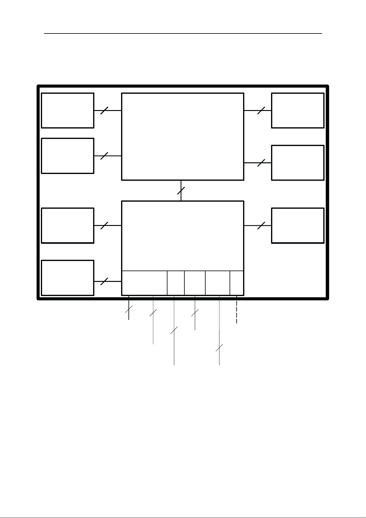
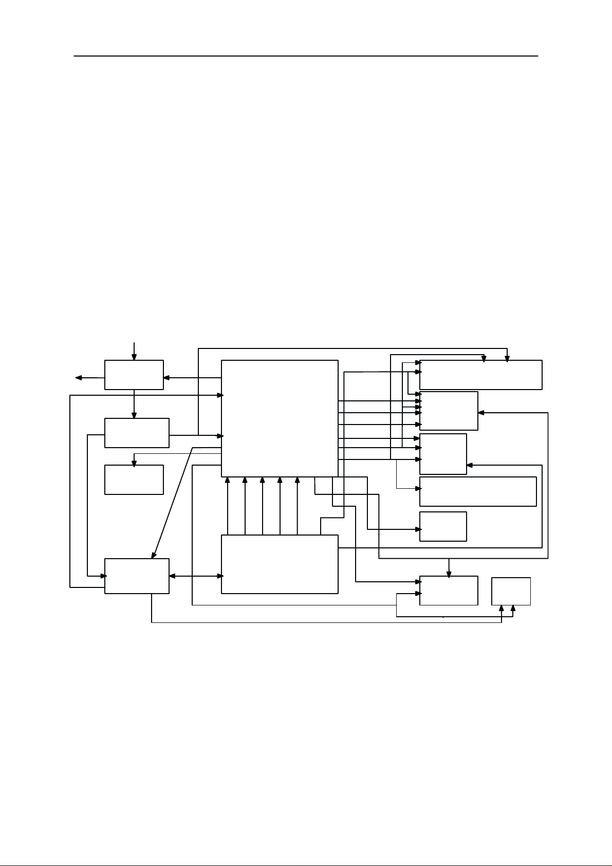
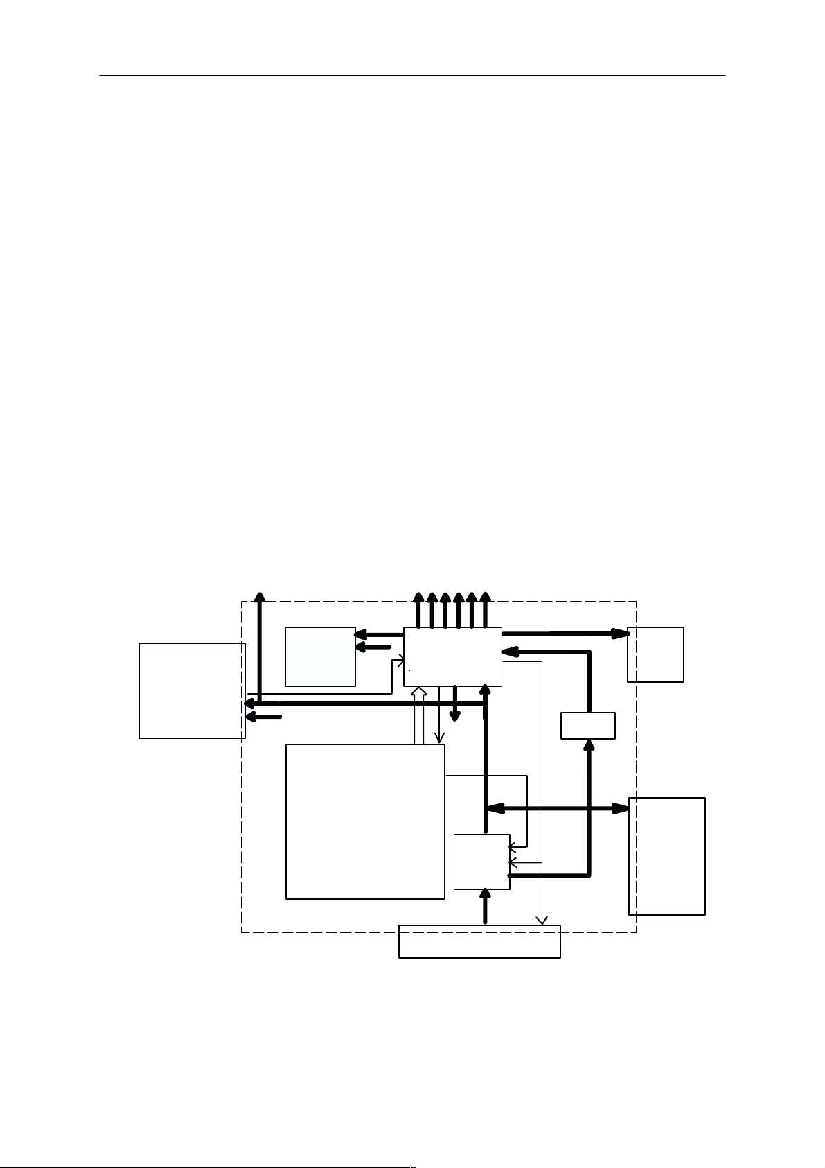
Interconnection Diagram
10 9
10
Keypad Display
Keypad
System Module
User Interface
Module
1
PWR Key
RTC
battery
UE4
28
2
System/RF
Module
2
Speaker
1
Antenna
MIC
connectors for external signals
2
System
Connector
3 + 3 6
Charger
accessories
UG3
RF SIM
2
SIM
card
external
antenna
battery
6
Battery
IR
NSM–1
IR Link
4
Issue 2 01/00
Page 3–7
Page 8
NSM–1
PAMS
System Module
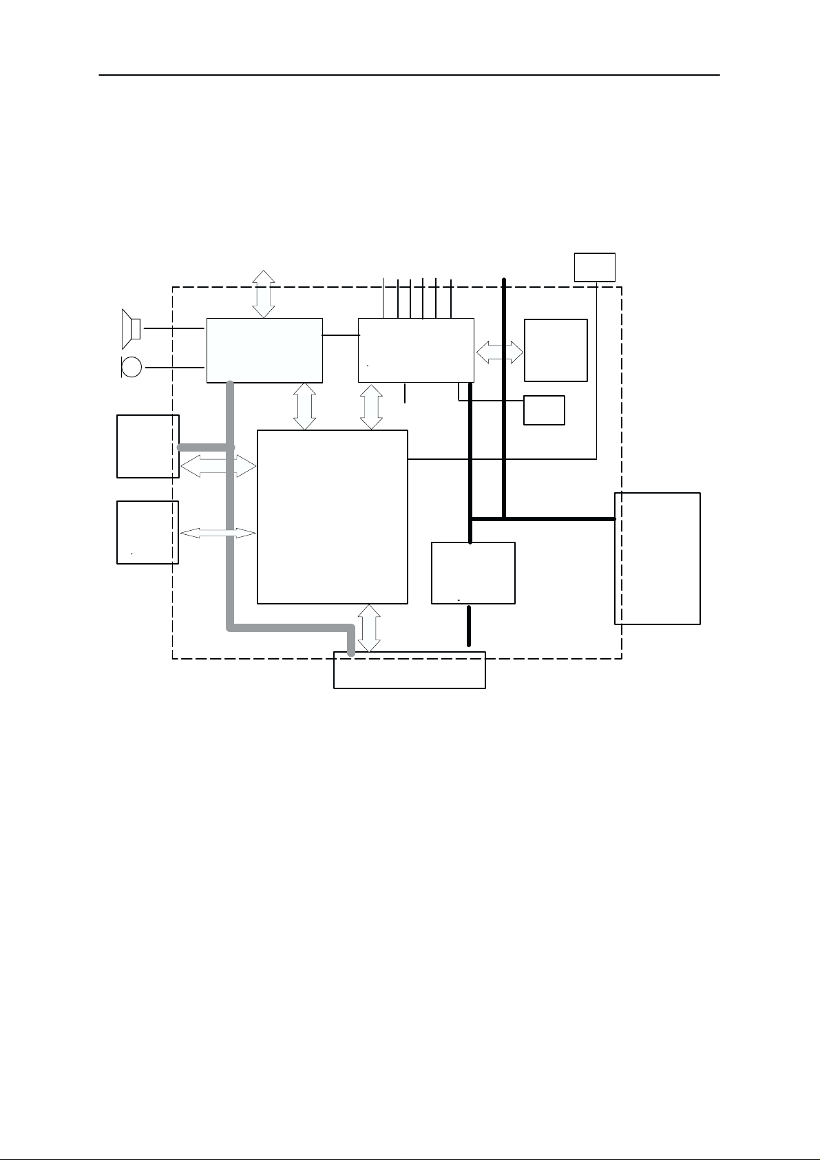
System Module
Circuit Description
The transceiver electronics consist of the Radio Module, RF + System
blocks, the UI PCB, the display module and audio components. The key-
pad and the display module are connected to the Radio Module with a
connectors. System blocks and RF blocks are interconnected with PCB
wiring. The Transceiver is connected to accessories via a bottom system
connector with charging and accessory control.
The System blocks provide the MCU, DSP and Logic control functions in
MAD ASIC, external memories, audio processing and RF control hard-
ware in COBBA ASIC. Power supply circuitry CCONT ASIC delivers oper-
ating voltages both for the System and the RF blocks.
The RF block is designed for a handportable phone which operates in the
GSM and DCS1800 systems. The purpose of the RF block is to receive
and demodulate the radio frequency signal from the base station and to
transmit a modulated RF signal to the base station. The SUMMA ASIC is
used for VHF and PLL functions. The CRFU3 ASIC is used at the front
end.
Technical Documentation
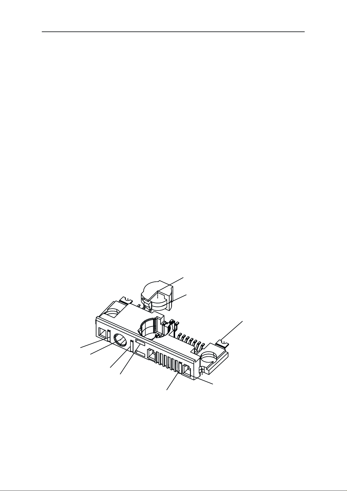
External and Internal Connectors
Contact 1
DC–jack
Contact 2
Microphone port
Contacts
3...8
Contact 9
Rubber boot
Microphone
Solderable element,
2 pcs
Cable/Cradle connector,
guiding/fixing hole, 3 pcs
Page 3–8
Issue 2 01/00
Page 9
PAMS
NSM–1
Technical Documentation
System Connector Contacts
Con-
tact
1 VIN Charger input volt-
DC–
JACK
DC–
JACK
Line
Sym-
bol
L_GND Charger ground
VIN Charger input volt-
Parameter Mini-
age
Charger input cur-
rent
input
age
Charger input cur-
rent
System Module
Typical
mum
7.1
720
7.24
320
0 0 0 V/ Supply ground
7.1
720
7.24
320
/ Nomi-
nal
8.4
800
7.6
370
8.4
800
7.6
370
Maxi-
mum
9.3
850
7.95
420
9.3
850
7.95
420
Unit / Notes
V/ Unloaded ACP–9 Charger
mA/ Supply current
V/ Unloaded ACP–7 Charger
mA/ Supply current
V/ Unloaded ACP–9 Charger
mA/ Supply current
V/ Unloaded ACP–7 Charger
mA/ Supply current
DC–
JACK
2 CHRG
Mic
ports
3 XMIC Input signal volt-
4 SGND Signal ground 0 0 mVrms
5 XEAR Output signal volt-
6 MBUS I/O low voltage
7 FBUS_RXInput low voltage
CHRG
CTRL
CTRL
Output high voltage
PWM frequency
Output high voltage
PWM frequency
Acoustic signal N/A N/A N/A Microphone sound ports
age
age
I/O high voltage
Input high voltage02.0
2.0
2.0
0
2.0
2.8 V/ Charger control (PWM)
32
2.8 V/ Charger control (PWM)
32
60 1 Vpp mVrms
80 1 Vpp mVrms
0.8
2.8
0.8
2.8
high
Hz /PWM frequency for
charger
high
Hz /PWM frequency for
charger
Serial bidirectional control
bus.
Baud rate 9600 Bit/s
V/ Fbus receive.
V/ Serial Data, Baud rate
9.6k–230.4kBit/s
8 FBUS_TXOutput low voltage
Output high voltage
9 L_GND Charger ground
input
Issue 2 01/00
0
2.0
0 0 0 V/ Supply ground
0.8
2.8
V/ Fbus transmit.
V/ Serial Data, Baud rate
9.6k–230.4kBit/s
Page 3–9
Page 10
NSM–1
PAMS
System Module
Technical Documentation
RF Connector Contacts
Con-
tact
1 EXT_ANT
2 GND
Line
Symbol
Parameter Mini-
mum
Impedance 50ohm tor,
Typical
/ Nomi-
nal
Maxi-
mum
External antenna connec0 V DC
Unit / Notes
Supply Voltages and Power Consumtion
Connector Line Symbol Minimum Typical /
Nominal
Charging VIN 7.1 8.4 9.3 V/ Travel charger,
Charging VIN 7.25 7.6 7.95 V/ Travel charger.
Charging I / VIN 720 800 850 mA/ Travel char-
Charging I / VIN 320 370 420 mA/ Travel char-
Maximum/
Peak
Unit / Notes
ACP–9
ACP–7
ger, ACP–9
ger, ACP–7
Page 3–10
Issue 2 01/00
Page 11
PAMS
NSM–1
Technical Documentation
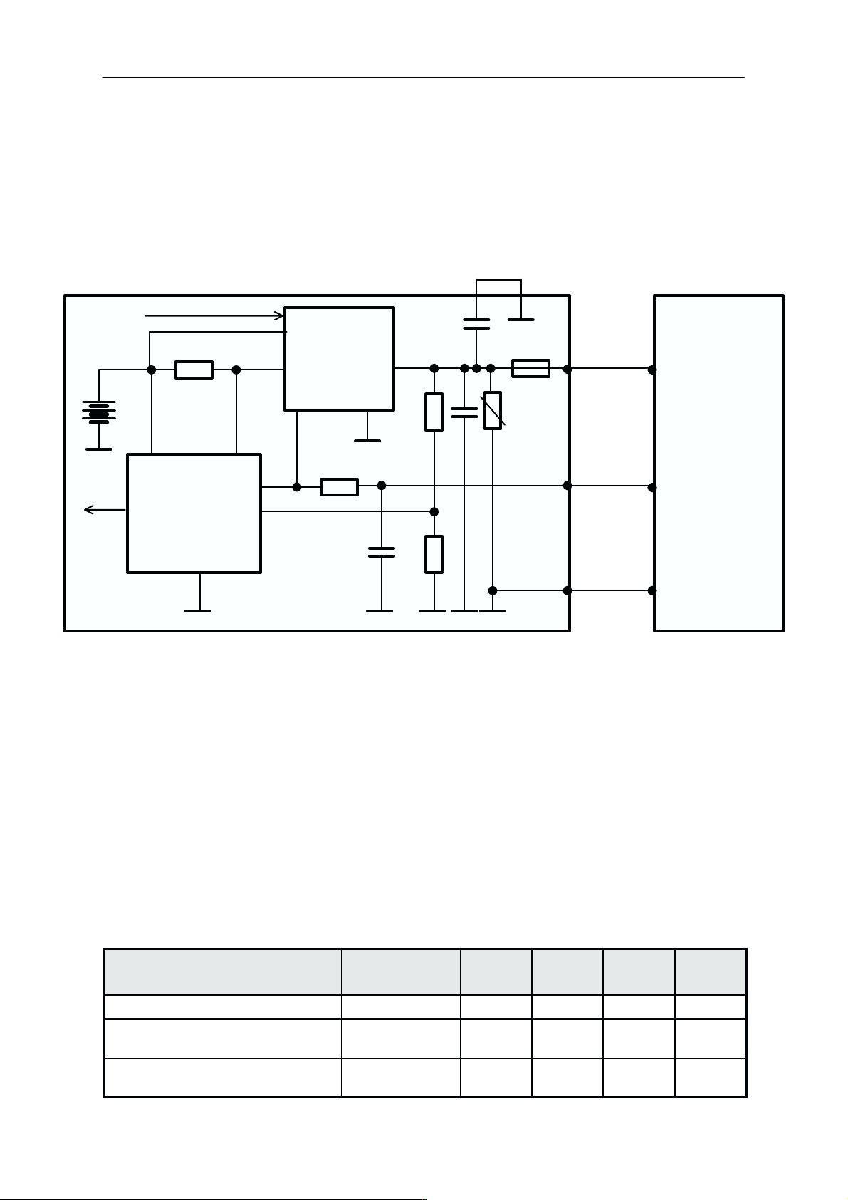
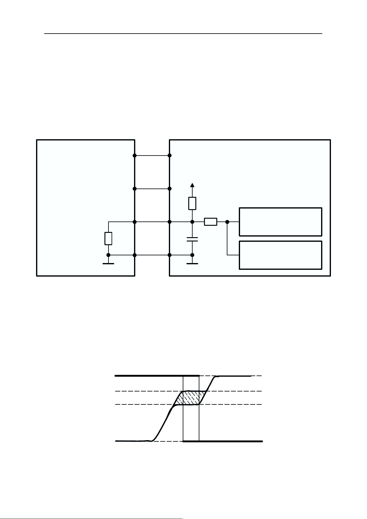
Power Distribution Diagram
The power supply is based on the ASIC circuit CCONT. The chip consists
of regulators and control circuits providing functions like power up, reset
and watchdog. External buffering is required to provide more current on
some blocks.
The MCU and the CCONT circuits control charging together, detection
being carried out by the CCONT and higher level intelligent control by the
MCU. The MCU measures battery voltage by means of the CCONT. The
CCONT also measures charger voltage, temperature and size of the battery.
Detailed power distribution diagrams are given in Baseband blocks and
RF blocks later in the document.
V_IN
PWM
CHARGING
CIRCUITRY
PWM
CCONT
TXP
VBAT
System Module
bias
power det
POWER AMPLIFIER
VBAT
BATTERY
VBAT
Note: VTX uses
a discrete
transistor to increse
VR7 output
capability
VSIM
SIM
V5V
VBAT
VBB
V
T
X
P
W
R
Y
X
N
P
P
W
W
R
R
S
R
S
C
I
X
M
O
P
P
W
R
T
W
X
R
P
MAD
VBB
UIF
PWRONX MEM
5V
VBB
V5V/VCP
VRX_2
VSYN_2
VRX_1
V_TX
VSYN_1
VSYN_1
VXO
VCOBBA
VREF
VBB
SUMMA
CRFU3
VREF
BAND SEL
RF SYNTHESIZERS
VCXO
COBBA
Issue 2 01/00
Page 3–11
Page 12
NSM–1
PAMS
System Module
Baseband Module
Block Diagram
TX/RX SIGNALS
COBBA
UI
COBBA SUPPLY
RF SUPPLIES
CCONT
BB SUPPLY
Technical Documentation
PA SUPPLY
32kHz
CLK
SLEEP CLOCK
SIM
13MHz
CLK
SYSTEM CLOCK
IR
AUDIOLINES
BASEBAND
Technical Summary
The baseband module consists of four asics, CHAPS, CCONT, COBBA–
GJ and MAD2, which take care of the baseband functions of NSM–1.
The baseband is running from a 2.8V power rail, which is supplied by a
power controlling asic. In the CCONT asic there are 6 individually controlled regulator outputs for RF–section and two outputs for the baseband. In addition there is one +5V power supply output (V5V) for flash
programming voltage and other purposes where a higher voltage is needed. The CCONT contains also a SIM interface, which supports both 3V
and 5V SIM–cards. A real time clock function is integrated into the
CCONT, which utilizes the same 32kHz clock supply as the sleep clock. A
backup power supply is provided for the RTC, which keeps the real time
clock running when the main battery is removed. The backup power supply is a rechargable polyacene battery. The backup time with this battery
is minimum of ten minutes.
MAD
+
MEMORIES
VBAT
BATTERY
CHAPS
SYSCON
Page 3–12
Issue 2 01/00
Page 13

PAMS
NSM–1
Technical Documentation
The interface between the baseband and the RF section is handled by a
specific asic. The COBBA asic provides A/D and D/A conversion of the
in–phase and quadrature receive and transmit signal paths and also A/D
and D/A conversions of received and transmitted audio signals to and
from the UI section. The COBBA supplies the analog TXC and AFC signals to rf section according to the MAD DSP digital control and converts
analog AGC into digital signal for the DSP. Data transmission between the
COBBA and the MAD is implemented using a parallel connection for high
speed signalling and a serial connection for PCM coded audio signals.
Digital speech processing is handled by the MAD asic. The COBBA asic
is a dual voltage circuit, the digital parts are running from the baseband
supply VBB and the analog parts are running from the analog supply
VCOBBA.
The baseband supports three external microphone inputs and two external earphone outputs. The inputs can be taken from an internal microphone, a headset microphone or from an external microphone signal
source. The microphone signals from different sources are connected to
separate inputs at the COBBA asic.
System Module
The output for the internal earphone is a dual ended type output capable
of driving a dynamic type speaker. Input and output signal source selection and gain control is performed inside the COBBA asic according to
control messages from the MAD. Keypad tones, DTMF, and other audio
tones are generated and encoded by the MAD and transmitted to the
COBBA for decoding. A buzzer and an external vibra alert control signals
are generated by the MAD with separate PWM outputs.
EMC shieding is implemented using a metallized plastic B–cover with a
conductive rubber seal on the ribs. On the other side the engine is
shielded with a frame having a conductive rubber on the inner walls,
which makes a contact to a ground ring of the engine board and a
ground plane of the UI–board. Heat generated by the circuitry will be conducted out via the PCB ground planes.
Issue 2 01/00
Page 3–13
Page 14
NSM–1
PAMS
System Module
Technical Documentation
Bottom Connector External Contacts
Contact Line Symbol Function
1 VIN Charger input voltage
DC–jack
side contact
(DC–plug ring)
DC–jack
center pin
DC–jack
side contact
(DC–plug jacket)
2 CHRG_CTRL Charger control output (from phone)
Microphone
acoustic ports
3 XMIC Accessory microphone signal input (to phone)
4 SGND Accessory signal ground
L_GND Charger ground
VIN Charger input voltage
CHRG_CTRL Charger control output (from phone)
Acoustic signal (to phone)
5 XEAR Accessory earphone signal output (from phone)
6 MBUS MBUS, bidirectional serial data i/o
7 FBUS_RX FBUS, unidirectional serial data input (to phone)
8 FBUS_TX FBUS, unidirectional serial data output (from phone)
9 L_GND Charger ground
Bottom Connector Signals
Pin Name Min Typ Max Unit Notes
1,3 VIN
2 L_GND 0 0 V Supply ground
7.25
3.25
320
7.1
3.25
720
7.6
3.6
370
8.4
3.6
800
7.95
16.9
3.95
420
9.3
3.95
850
V
V
V
mA
V
V
mA
Unloaded ACP–7 Charger (5kohms
load)
Peak output voltage (5kohms load)
Loaded output voltage (10ohms load)
Supply current
Unloaded ACP–9 Charger
Loaded output voltage (10ohms load)
Supply current
4,5 CHRG_
CTRL
6 MICP N/A see section Internal microphone
7 MICN N/A see section Internal microphone
Page 3–14
0 0.5 V Charger control PWM low
2.0 2.85 V Charger control PWM high
32 Hz PWM frequency for a fast charger
1 99 % PWM duty cycle
Issue 2 01/00
Page 15
PAMS
NSM–1
Technical Documentation
8 XMIC
HMIC 0 3.2 29.3 mV Microphone signal
9 SGND
10 XEAR
2.0 2.2 kΩ Input AC impedance
1.47 1.55 V Mute (output DC level)
2.5 2.85 V Unmute (output DC level)
100 600 µA Bias current
System Module
NotesUnitMaxTypMinNamePin
1 Vpp Maximum signal level
58 490 mV Maximum signal level
Connected to COBBA MIC3P input
47 Ω Output AC impedance (ref. GND)
10 µF Series output capacitance
380 Ω Resistance to phone ground
47 Ω Output AC impedance (ref. GND)
10 µF Series output capacitance
16 300 Ω Load AC impedance to SGND (Head-
set)
4.7 10 kΩ Load AC impedance to SGND (Accessory)
1.0 Vpp Maximum output level (no load)
22 626 mV Output signal level
10 kΩ Load DC resistance to SGND (Acces-
sory)
16 1500 Ω Load DC resistance to SGND (Head-
set)
2.8 V DC voltage (47k pull–up to VBB)
HEAR 28 626 mV Earphone signal (HF– HFCM)
Connected to COBBA HF output
11 MBUS 0 logic low 0.8 V Serial bidirectional control bus.
2.0 logic high 2.85
12 FBUS_RX 0 logic low 0.8 V Fbus receive. Serial Data
2.0 logic high 2.85
13 FBUS_TX 0 logic low 0.5 V Fbus transmit. Serial Data
2.0 logic high 2.85
Baud rate 9600 Bit/s
Phone has a 4k7 pullup resistor
Baud rate 9.6k–230.4kBit/s
Phone has a 220k pulldown resistor
Baud rate 9.6k–230.4kBit/s
Phone has a 47k pullup resistor
14 GND 0 0.3 V Supply ground
Issue 2 01/00
Page 3–15
Page 16
NSM–1
PAMS
System Module
Technical Documentation
Battery Connector
Pin Name Min Typ Max Unit Notes
1 BVOLT 3.0 3.6 4.5 V Battery voltage
2 BSI
3 BTEMP
5.0
5.3
0 2.85 V Battery size indication
2.2 18 kohm Battery indication resistor (Ni battery)
20 22 24 kohm Battery indication resistor (service battery)
27 51 kohm Battery indication resistor (4.1V Lithium
68 91 kohm Battery indication resistor (4.2V Lithium bat-
0 1.4 V Battery temperature indication
Maximum voltage in call state with charger
Maximum voltage in idle state with charger
Phone has 100kohm pull up resistor.
SIM Card removal detection
(Treshold is 2.4V@VBB=2.8V)
battery)
tery)
Phone has a 100k (+–5%) pullup resistor,
Battery package has a NTC pulldown resis-
tor:
47k+–5%@+25C , B=4050+–3%
2.1
5
1.9
90
0 1 kohm Local mode initialization (in production)
20 22 25 kHz PWM control to VIBRA BA TTERY
4 BGND 0 0 V Battery ground
10
100
3
20
2.85
200
V
ms
V
ms
Phone power up by battery (input)
Power up pulse width
Battery power up by phone (output)
Power up pulse width
Page 3–16
Issue 2 01/00
Page 17
PAMS
NSM–1
Technical Documentation
System Module
SIM Card Connector
Pin Name Parameter Min Typ Max Unit Notes
4 GND GND 0 0 V Ground
3, 5 VSIM 5V SIM Card
3V SIM Card
6 DATA 5V Vin/Vout
3V Vin/Vout
2 SIMRST 5V SIM Card
3V SIM Card
1 SIMCLK Frequency
Trise/Tfall
4.8
2.8
4.0
0
2.8
0
4.0
2.8
5.0
3.0
”1”
”0”
”1”
”0”
”1”
”1”
3.25
5.2
3.2
VSIM
0.5
VSIM
0.5
VSIM
VSIM
25
V Supply voltage
V SIM data
Trise/Tfall max 1us
V SIM reset
MHz
ns
SIM clock
Internal Microphone
Pin Name Min Typ Max Unit Notes
6 MICP 0.55 4.1 mV Connected to COBBA MIC2N input. The
maximum value corresponds to1 kHz, 0
dBmO network level with input amplifier
gain set to 32 dB. typical value is maximum value – 16 dB.
7 MICN 0.55 4.1 mV Connected to COBBA MIC2P input. The
maximum value corresponds to1 kHz, 0
dBmO network level with input amplifier
gain set to 32 dB. typical value is maximum value – 16 dB.
Infrared Module Connections
An infrared transceiver module is designed to substitute an electrical
cable between the phone and a PC. The infrared transceiver module is a
stand alone component capable to perform infrared transmitting and receiving functions by transforming signals transmitted in infrared light from
and to electrical data pulses running in two wire asyncronous databus. In
DCT3 the module is placed inside the phone at the top of the phone.
Signal Parameter Min Typ Max Unit Notes
IRON IR–module on/off 2.0 2.85 V Iout@2mA
FBUS_RX
FBUS_TX
IR receive pulse 0 0.8 V
IR receive no pulse 2.0 2.85 V
IR transmit pulse 2.0 2.85 V Iout@2mA
IR transmit no pulse 0 0.5 V
Issue 2 01/00
Page 3–17
Page 18
NSM–1
PAMS
System Module
Technical Documentation
RTC Backup Battery
The RTC block in CCONT needs a power backup to keep the clock running when the phone battery is disconnected. The backup power is supplied from a rechargable polyacene battery that can keep the clock running minimum of 10 minutes. The backup battery is charged from the
main battery through CHAPS.
Signal Parameter Min Typ Max Unit Notes
VBACK
VBACK
Backup battery charging from CHAPS
Backup battery charging from CHAPS
Backup battery supply
to CCONT
Backup battery supply
to CCONT
3.02 3.15 3.28 V
100 200 500 uA Vout@VBAT–0.2V
2 3.28 V Battery capacity
65uAh
80 uA
Buzzer
Signal Maximum
BuzzPWM /
BUZZER
Input
output cur-
rent
2mA 2.5V 0.2V 0...50 (128 lin-
high level
Input
low level
Level (PWM)
range, %
ear steps)
Frequency
range, Hz
440...4700
Page 3–18
Issue 2 01/00
Page 19
PAMS
NSM–1
Technical Documentation
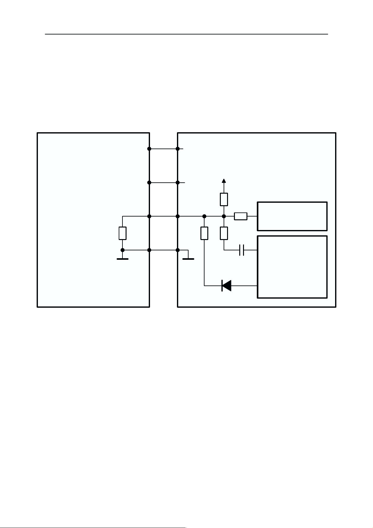
Baseband Power Distribution
Functional Description
In normal operation the baseband is powered from the phone‘s battery.
The battery consists of three Nickel Metal Hydride cells. There is also a
possibility to use batteries consisting of one Lithium–Ion cell. An external
charger can be used for recharging the battery and supplying power to
the phone. The charger can be either a standard charger that can deliver
around 400 mA or so called performance charger, which can deliver supply current up to 850 mA.
The baseband contains components that control power distribution to
whole phone excluding those parts that use continuous battery supply.
The battery feeds power directly to three parts of the system: CCONT,
power amplifier, and UI (buzzer and display and keyboard lights). Figure
below shows a block diagram of the power distribution.
The power management circuit CHAPS provides protection agains overvoltages, charger failures and pirate chargers etc. that would otherwise
cause damage to the phone.
System Module
PA SUPPLY
VCOBBA
COBBA
UI
VBAT
VBB
BASEBAND
VBB
MAD
+
MEMORIES
RF SUPPLIES
CCONT
PWRONX
CNTVR
BOTTOM CONNECTOR
PWM
VBB
PURX
LIM
CHAPS
VIN
VSIM
VBAT
RTC
BACKUP
SIM
BATTERY
Battery charging
The electrical specifications give the idle voltages produced by the acceptable chargers at the DC connector input. The absolute maximum in-
Issue 2 01/00
Page 3–19
Page 20
NSM–1
PAMS
System Module
MAD
VBAT
MAD
CCONTINT
Technical Documentation
put voltage is 30V due to the transient suppressor that is protecting the
charger input. At phone end there is no difference between a plug–in
charger or a desktop charger. The DC–jack pins and bottom connector
charging pads are connected together inside the phone.
0R22
PWM_OUT
CCONT
GND
ICHAR
VCHAR
LIM
VOUT
CHAPS
RSENSE
PWM
VCH
GND
47k
22k
1n
4k7
27p
1u
1,5A
30V
VIN
CHRG_CTRL
L_GND
CHARGER
NOT IN
ACP–7
TRANSCEIVER
Startup Charging
When a charger is connected, the CHAPS is supplying a startup current
minimum of 130mA to the phone. The startup current provides initial
charging to a phone with an empty battery. Startup circuit charges the
battery until the battery voltage level is reaches 3.0V (+/– 0.1V) and the
CCONT releases the PURX reset signal and program execution starts.
Charging mode is changed from startup charging to PWM charging that is
controlled by the MCU software. If the battery voltage reaches 3.55V
(3.75V maximum) before the program has taken control over the charging, the startup current is switched off. The startup current is switched on
again when the battery voltage is sunken 100mV (nominal).
Parameter Symbol Min Typ Max Unit
VOUT Start– up mode cutoff limit Vstart 3.45 3.55 3.75 V
VOUT Start– up mode hysteresis
NOTE: Cout = 4.7 uF
Start–up regulator output current
VOUT = 0V ... Vstart
Vstarthys 80 100 200 mV
Istart 130 165 200 mA
Page 3–20
Issue 2 01/00
Page 21
PAMS
NSM–1
Technical Documentation
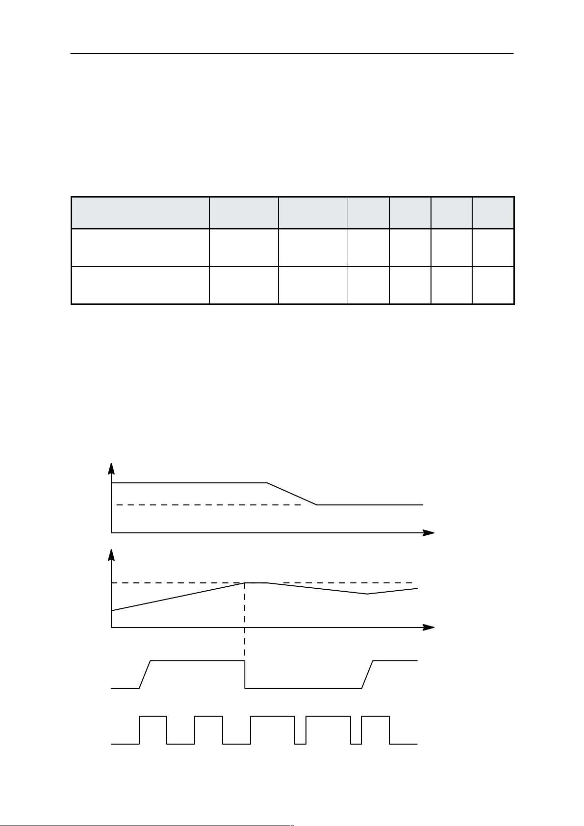
Battery Overvoltage Protection
Output overvoltage protection is used to protect phone from damage.
This function is also used to define the protection cutoff voltage for different battery types (Li or Ni). The power switch is immediately turned OFF if
the voltage in VOUT rises above the selected limit VLIM1 or VLIM2.
Parameter Symbol LIM input Min Typ Max Unit
Output voltage cutoff limit
(during transmission or Li–
battery)
Output voltage cutoff limit
(no transmission or Ni–bat-
tery)
VLIM1 LOW 4.4 4.6 4.8 V
VLIM2 HIGH 4.8 5.0 5.2 V
The voltage limit (VLIM1 or VLIM2) is selected by logic LOW or logic
HIGH on the CHAPS (N101) LIM– input pin. Default value is lower limit
VLIM1.
System Module
VCH
VCH<VOUT
VOUT
VLIM1 or VLIM2
When the switch in output overvoltage situation has once turned OFF, it
stays OFF until the the battery voltage falls below VLIM1 (or VLIM2) and
PWM = LOW is detected. The switch can be turned on again by setting
PWM = HIGH.
t
t
SWITCH
PWM (32Hz)
Issue 2 01/00
ON OFF
ON
Page 3–21
Page 22
NSM–1
PAMS
System Module
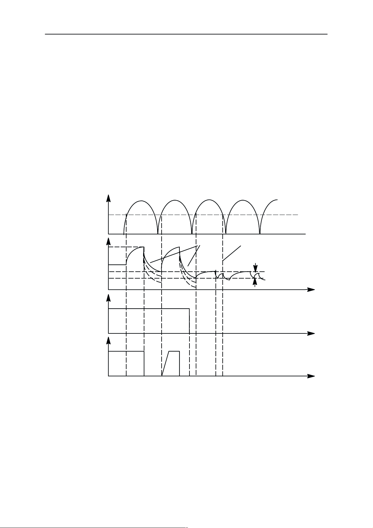
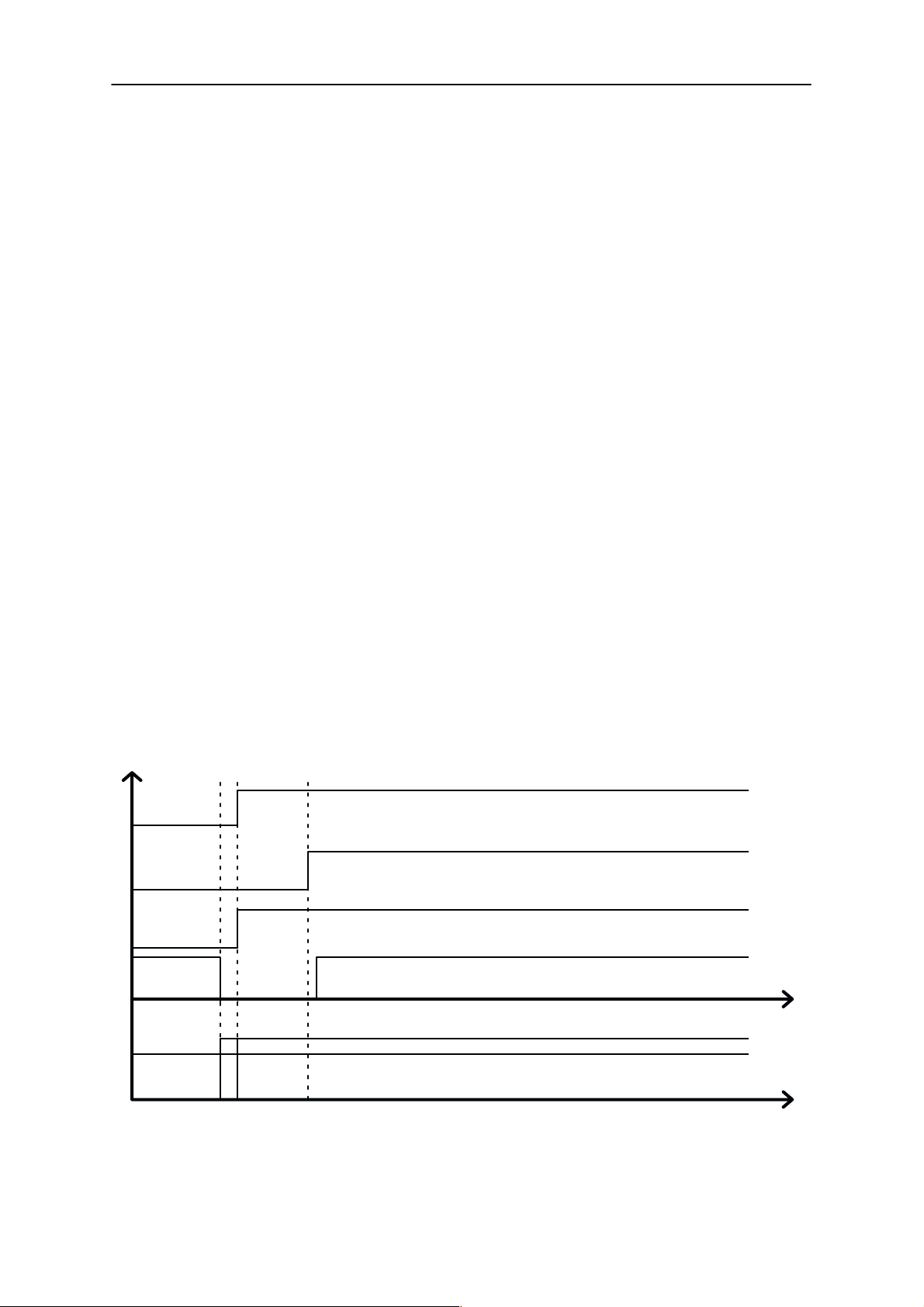
Battery Removal During Charging
Output overvoltage protection is also needed in case the main battery is
removed when charger connected or charger is connected before the battery is connected to the phone.
With a charger connected, if VOUT exceeds VLIM1 (or VLIM2), CHAPS
turns switch OFF until the charger input has sunken below Vpor (nominal
3.0V, maximum 3.4V). MCU software will stop the charging (turn off
PWM) when it detects that battery has been removed. The CHAPS remains in protection state as long as PWM stays HIGH after the output
overvoltage situation has occured.
VCH
(Standard
Charger)
VOUT
Vpor
VLIM
4V
Vstart
Droop depends on load
& C in phone
Technical Documentation
Istart off due to VCH<Vpor
Vstarthys
PWM
SWITCH
1.1Battery removed, (standard) charger connected, VOUT rises (follows charger voltage)
2. VOUT exceeds limit VLIM(X), switch is turned immediately OFF
3.3VOUT falls (because no battery) , also VCH<Vpor (standard chargers full–rectified
4. Software sets PWM = LOW –> CHAPS does not enter PWM mode
5. PWM low –> Startup mode, startup current flows until Vstart limit reached
6. VOUT exceeds limit Vstart, Istart is turned off
7. VCH falls below Vpor
”1”
”0”
ON
OFF
2
output). When VCH > Vpor and VOUT < VLIM(X) –> switch turned on again (also PWM
is still HIGH) and VOUT again exceeds VLIM(X).
5
4
6
7
t
t
t
Page 3–22
Issue 2 01/00
Page 23
PAMS
NSM–1
Technical Documentation
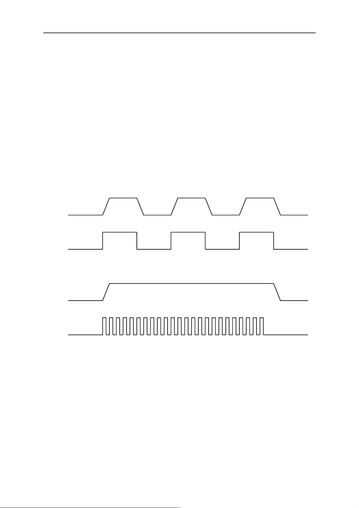
Different PWM Frequencies ( 1Hz and 32 Hz)
When a travel charger (2– wire charger) is used, the power switch is
turned ON and OFF by the PWM input when the PWM rate is 1Hz. When
PWM is HIGH, the switch is ON and the output current Iout = charger current – CHAPS supply current. When PWM is LOW, the switch is OFF and
the output current Iout = 0. To prevent the switching transients inducing
noise in audio circuitry of the phone soft switching is used.
The performance travel charger (3– wire charger) is controlled with PWM
at a frequency of 32Hz. When the PWM rate is 32Hz CHAPS keeps the
power switch continuously in the ON state.
SWITCH
ON ONON OFF OFF
System Module
PWM (1Hz)
SWITCH
PWM (32Hz)
ON
Issue 2 01/00
Page 3–23
Page 24
NSM–1
PAMS
System Module
Battery Identification
Different battery types are identified by a pulldown resistor inside the battery pack. The BSI line inside transceiver has a 100k pullup to VBB. The
MCU can identify the battery by reading the BSI line DC–voltage level
with a CCONT (N100) A/D–converter.
BATTERY
BVOLT
BTEMP
BSI
VBB
2.8V
100k
10k
Technical Documentation
TRANSCEIVER
BSI
CCONT
The battery identification line is used also for battery removal detection.
The BSI line is connected to a SIMCardDetX line of MAD2 (D200). SIMCardDetX is a threshold detector with a nominal input switching level
0.85xVcc for a rising edge and 0.55xVcc for a falling edge. The battery
removal detection is used as a trigger to power down the SIM card before
the power is lost. The BSI contact in the battery pack is made 0.7mm
shorter than the supply voltage contacts so that there is a delay between
battery removal detection and supply power off,
Vcc
0.850.05 Vcc
0.550.05 Vcc
R
s
BGND
10n
SIMCardDetX
MAD
Page 3–24
GND
SIMCARDDETX
S
IGOUT
Issue 2 01/00
Page 25
PAMS
NSM–1
Technical Documentation
Battery Temperature
The battery temperature is measured with a NTC inside the battery pack.
The BTEMP line inside transceiver has a 100k pullup to VREF. The MCU
can calculate the battery temperature by reading the BTEMP line DC–
voltage level with a CCONT (N100) A/D–converter.
BATTERY
BVOLT
BSI
BTEMP
TRANSCEIVER
VREF
100k
10k
System Module
BTEMP
CCONT
R
T
NTC
Supply Voltage Regulators
The heart of the power distrubution is the CCONT. It includes all the voltage regulators and feeds the power to the whole system. The baseband
digital parts are powered from the VBB regulator which provides 2.8V
baseband supply. The baseband regulator is active always when the
phone is powered on. The VBB baseband regulator feeds MAD and memories, COBBA digital parts and the LCD driver in the UI section. There is
a separate regulator for a SIM card. The regulator is selectable between
3V and 5V and controlled by the SIMPwr line from MAD to CCONT. The
COBBA analog parts are powered from a dedicated 2.8V supply VCOBBA. The CCONT supplies also 5V for RF and for flash VPP. The CCONT
contains a real time clock function, which is powered from a RTC backup
when the main battery is disconnected.
BGND
1k
1k
10n
VibraPWM
MAD
MCUGenIO4
Issue 2 01/00
Page 3–25
Page 26
NSM–1
PAMS
System Module
The RTC backup is rechargable polyacene battery, which has a capacity
of 50uAh (@3V/2V) The battery is charged from the main battery voltage
by the CHAPS when the main battery voltage is over 3.2V. The charging
current is 200uA (nominal).
Operating mode Vref RF REG VCOB-
BA
Power off Off Off Off Off Off Pull
Power on On On/Off On On On On/Off
Reset On Off
VR1 On
Sleep On Off On On On On/Off
NOTE:
On On Off Pull
Technical Documentation
VBB VSIM SIMIF
down
down
CCONT includes also five additional 2.8V regulators providing power to
the RF section. These regulators can be controlled either by the direct
control signals from MAD or by the RF regulator control register in
CCONT which MAD can update. Below are the listed the MAD control
lines and the regulators they are controlling.
– TxPwr controls VTX regulator (VR5)
– RxPwr controls VRX regulator (VR2)
– SynthPwr controls VSYN_1 and VSYN_2 regulators (VR4 and VR3)
– VCXOPwr controls VXO regulator (VR1)
CCONT generates also a 1.5 V reference voltage VREF to COBBA,
SUMMA and CRFU3. The VREF voltage is also used as a reference to
some of the CCONT A/D converters.
In additon to the above mentioned signals MAD includes also TXP control
signal which goes to SUMMA power control block and to the power amplifier. The transmitter power control TXC is led from COBBA to SUMMA.
Page 3–26
Issue 2 01/00
Page 27
PAMS
NSM–1
Technical Documentation
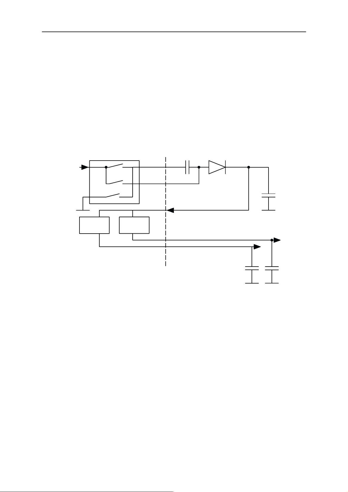
Switched Mode Supply VSIM
There is a switched mode supply for SIM–interface. SIM voltage is selected via serial IO. The 5V SMR can be switched on independently of the
SIM voltage selection, but can’t be switched off when VSIM voltage value
is set to 5V.
NOTE: VSIM and V5V can give together a total of 30mA.
In the next figure the principle of the SMR / VSIM–functions is shown.
CCONT External
VBAT
System Module
V5V_4
V5V_3
V5V_2
Power Up
VSIM
The baseband is powered up by:
1. Pressing the power key, that generates a PWRONX interrupt
2. Connecting a charger to the phone. The CCONT recognizes
3. A RTC interrupt. If the real time clock is set to alarm and the
5V reg
V5V
signal from the power key to the CCONT, which starts the power up procedure.
the charger from the VCHAR voltage and starts the power up
procedure.
phone is switched off, the RTC generates an interrupt signal,
when the alarm is gone off. The RTC interrupt signal is connected to the PWRONX line to give a power on signal to the
CCONT just like the power key.
5/3V
5V
Issue 2 01/00
4. A battery interrupt. Intelligent battery packs have a possibility
to power up the phone. When the battery gives a short (10ms)
voltage pulse through the BTEMP pin, the CCONT wakes up
and starts the power on procedure.
Page 3–27
Page 28
NSM–1
PAMS
System Module
Power up with a charger
When the charger is connected CCONT will switch on the CCONT digital
voltage as soon as the battery voltage exeeds 3.0V. The reset for
CCONT’s digital parts is released when the operating voltage is stabilized
( 50 us from switching on the voltages). Operating voltage for VCXO is
also switched on. The counter in CCONT digital section will keep MAD in
reset for 62 ms (PURX) to make sure that the clock provided by VCXO is
stable. After this delay MAD reset is relased, and VCXO –control
(SLEEPX) is given to MAD. The diagram assumes empty battery, but the
situation would be the same with full battery:
When the phone is powered up with an empty battery pack using the
standard charger, the charger may not supply enough current for standard powerup procedure and the powerup must be delayed.
Power Up With The Power Switch (PWRONX)
Technical Documentation
When the power on switch is pressed the PWRONX signal will go low.
CCONT will switch on the CCONT digital section and VCXO as was the
case with the charger driven power up. If PWRONX is low when the 64
ms delay expires, PURX is released and SLEEPX control goes to MAD. If
PWRONX is not low when 64 ms expires, PURX will not be released, and
CCONT will go to power off ( digital section will send power off signal to
analog parts)
SLEEPX
PURX
CCPURX
PWRONX
12 3
1:Power switch pressed ==> Digital voltages on in CCONT (VBB)
2: CCONT digital reset released. VCXO turned on
3: 62 ms delay to see if power switch is still pressed.
Page 3–28
VR1,VR6
VBB (2.8V)
Vchar
Issue 2 01/00
Page 29

PAMS
NSM–1
Technical Documentation
Power Up by RTC
RTC ( internal in CCONT) can power the phone up by changing RTCPwr to
logical ”1”. RTCPwr is an internal signal from the CCONT digital section.
Power Up by IBI
IBI can power CCONT up by sending a short pulse to logical ”1”. RTCPwr is
an internal signal from the CCONT digital section.
Acting Dead
If the phone is off when the charger is connected, the phone is powered
on but enters a state called ”acting dead”. To the user the phone acts as if
it was switched off. A battery charging alert is given and/or a battery
charging indication on the display is shown to acknowledge the user that
the battery is being charged.
Active Mode
System Module
In the active mode the phone is in normal operation, scanning for channels, listening to a base station, transmitting and processing information.
All the CCONT regulators are operating. There are several substates in
the active mode depending on if the phone is in burst reception, burst
transmission, if DSP is working etc..
Sleep Mode
In the sleep mode, all the regulators except the baseband VBB, VCOBBA,
and the SIM card VSIM regulators are off. Sleep mode is activated by the
MAD after MCU and DSP clocks have been switched off. The voltage regulators for the RF section are switched off and the VCXO power control,
VCXOPwr is set low. In this state only the 32 kHz sleep clock oscillator in
CCONT is running. The flash memory power down input is connected to
the ExtSysResetX signal, and the flash is deep powered down during the
sleep mode.
The sleep mode is exited either by the expiration of a sleep clock counter
in the MAD or by some external interrupt, generated by a charger connection, key press, headset connection etc. The MAD starts the wake up
sequence and sets the VCXOPwr and ExtSysResetX control high. After
VCXO settling time other regulators and clocks are enabled for active
mode.
If the battery pack is disconnect during the sleep mode, the CCONT pulls
the SIM interface lines low as there is no time to wake up the MCU.
Charging
Charging can be performed in any operating mode. The charging algorithm is dependent on the used battery technology. The battery type is in-
Issue 2 01/00
Page 3–29
Page 30

NSM–1
PAMS
System Module
dicated by a resistor inside the battery pack. The resistor value corresponds to a specific battery capacity. This capacity value is related to the
battery technology as different capacity values are achieved by using different battery technology.
The battery voltage, temperature, size and current are measured by the
CCONT controlled by the charging software running in the MAD.
The power management circuitry controls the charging current delivered
from the charger to the battery. Charging is controlled with a PWM input signal, generated by the CCONT. The PWM pulse width is controlled by the
MAD and sent to the CCONT through a serial data bus. The battery voltage
rise is limited by turning the CHAPS switch off when the battery voltage has
reached 4.2V (LiIon) or 5.2V (NiMH, 5V in call mode). Charging current is
monitored by measuring the voltage drop across a 220mohm resistor.
Power Off
The baseband is powered down by:
Technical Documentation
1. Pressing the power key, that is monitored by the MAD, which
starts the power down procedure.
2. If the battery voltage is dropped below the operation limit, either by not charging it or by removing the battery.
3. Letting the CCONT watchdog expire, which switches off all
CCONT regulators and the phone is powered down.
4. Setting the real time clock to power off the phone by a timer.
The RTC generates an interrupt signal, when the alarm is gone
off. The RTC interrupt signal is connected to the PWRONX line
to give a power off signal to the CCONT just like the power key.
The power down is controlled by the MAD. When the power key has been
pressed long enough or the battery voltage is dropped below the limit the
MCU initiates a power down procedure and disconnects the SIM power.
Then the MCU outputs a system reset signal and resets the DSP. If there is
no charger connected the MCU writes a short delay to CCONT watchdog
and resets itself. After the set delay the CCONT watchdog expires, which
activates the PURX and all regulators are switched off and the phone is
powered down by the CCONT.
If a charger is connected when the power key is pressed the phone enters into the acting dead mode.
Watchdog
Page 3–30
The Watchdog block inside CCONT contains a watchdog counter and
some additional logic which are used for controlling the power on and
power off procedures of CCONT. Watchdog output is disabled when
WDDisX pin is tied low. The WD-counter runs during that time, though.
Watchdog counter is reset internally to 32s at power up. Normally it is reset by MAD writing a control word to the WDReg.
Issue 2 01/00
Page 31

PAMS
NSM–1
Technical Documentation
Audio control
The audio control and processing is taken care by the COBBA–GJ, which
contains the audio and RF codecs, and the MAD2, which contains the
MCU, ASIC and DSP blocks handling and processing the audio signals. A
detailed audio specification can be found from document
MICP/N
System
Connector
Bias +
EMC
EMC + Acc.
XMIC
SGND
XEAR
Interf.
EMC
Preamp
MIC2
MIC1
MIC3
HFCM
AuxOut
HF
EAR
Multipl.Premult.
Amp Multipl.
COBBA
Pre
& LP
LP
System Module
MAD
DSP
A
D
D
A
MCU
Buzzer
Driver
Circuit
Buzzer
The baseband supports three microphone inputs and two earphone outputs. The inputs can be taken from an internal microphone, a headset microphone or from an external microphone signal source. The microphone
signals from different sources are connected to separate inputs at the
COBBA–GJ asic. Inputs for the microphone signals are differential type.
The MIC1 inputs are used for a headset microphone that can be connected directly to the system connector. The internal microphone is connected to MIC2 inputs and an external pre–amplified microphone (handset/handfree) signal is connected to the MIC3 inputs. In COBBA there are
also three audio signal outputs of which dual ended EAR lines are used
for internal earpiece and HF line for accessory audio output. The third audio output AUXOUT is used only for bias supply to the headset microphone. As a difference to DCT2 generation the SGND ( = HFCM at COBBA) does not supply audio signal (only common mode). Therefore there
are no electrical loopback echo from downlink to uplink.
The output for the internal earphone is a dual ended type output capable
of driving a dynamic type speaker. The output for the external accessory
and the headset is single ended with a dedicated signal ground SGND.
Input and output signal source selection and gain control is performed inside the COBBA–GJ asic according to control messages from the MAD2.
Keypad tones, DTMF, and other audio tones are generated and encoded
by the MAD2 and transmitted to the COBBA–GJ for decoding.
Issue 2 01/00
Page 3–31
Page 32

NSM–1
PAMS
System Module
External Audio Connections
The external audio connections are presented in figure 16. A headset can
be connected directly to the system connector. The headset microphone
bias is supplied from COBBA AUXOUT output and fed to microphone
through XMIC line. The 330ohm resistor from SGND line to AGND provides a return path for the bias current.
Baseband
HookDet
MAD
HeadDet
1u
Technical Documentation
2.8 V
47k
22k
22k
1u
CCONT
AUXOUT
COBBA
EAD
HFC
M
MIC1
N
MIC1
P
MIC3
N
MIC3
P
2.8 V
47k
47R
1m
10m
H
F
10m
33n
33n
33n
33n
47R
47R
330R
2k2
2k2
2k2
XEAR
SGN
D
XMI
C
Page 3–32
Issue 2 01/00
Page 33

PAMS
NSM–1
Technical Documentation
System Module
Analog Audio Accessory Detection
In XEAR signal there is a 47 kW pullup in the transceiver and 6.8 kW
pull–down to SGND in accessory. The XEAR is pulled down when an
accessory is connected, and pulled up when disconnected. The XEAR is
connected to the HookDet line (in MAD), an interrupt is given due to both
connection and disconnection. There is filtering between XEAR and
HookDet to prevent audio signal giving unwanted interrupts.
External accessory notices powered–up phone by detecting voltage in
XMIC line. In Table 23 there is a truth table for detection signals.
Accessory connected HookDet HeadDet Notes
No accessory connected High High Pullups in the transceiver
Headset HDC–9 with a button switch
pressed
Headset HDC–9 with a button switch re-
leased
Handsfree (HFU–1) Low High XEAR loaded (dc)
Low Low XEAR and XMIC loaded (dc)
High Low *) XEAR unloaded (dc)
Headset Detection
The external headset device is connected to the system connector, from
which the signals are routed to COBBA headset microphone inputs and
earphone outputs. In the XMIC line there is a (47 + 2.2) kW pullup in the
transceiver. The microphone is a low resistancepulldown compared to
the transceiver pullup.
When there is no call going, the AUXOUT is in high impedance state and
the XMIC is pulled up. When a headset is connected, the XMIC is pulled
down. The XMIC is connected to the HeadDet line (in MAD), an interrupt
is given due to both connection and disconnection. There is filtering between the XMIC and the HeadDet to prevent audio signal giving unwanted interrupts (when an accessory is connected).
In the XEAR line there is a 47 kW pullup in the transceiver. The earphone
is a low resistance pulldown compared to the transceiver pullup. When a
remote control switch is open, there is a capacitor in series with the earphone, so the XEAR (and HookDet) is pulled up by the phone. When the
switch is closed, the XEAR (and HookDet) is pulled down via the earphone. So both press and release of the button gives an interrupt.
During a call there is a bias voltage (1.5 V) in the AUXOUT, and the
HeadDet cannot be used. The headset interrupts should to be disabled
during a call and the EAD line (AD converter in CCONT) should be polled
to see if the headset is disconnected.
Issue 2 01/00
Page 3–33
Page 34

NSM–1
PAMS
System Module
Internal Audio Connections
The speech coding functions are performed by the DSP in the MAD2 and
the coded speech blocks are transferred to the COBBA–GJ for digital to
analog conversion, down link direction. In the up link direction the PCM
coded speech blocks are read from the COBBA–GJ by the DSP.
There are two separate interfaces between MAD2 and COBBA–GJ: a
parallel bus and a serial bus. The parallel bus has 12 data bits, 4 address
bits, read and write strobes and a data available strobe. The parallel interface is used to transfer all the COBBA–GJ control information (both the
RFI part and the audio part) and the transmit and receive samples. The
serial interface between MAD2 and COBBA–GJ includes transmit and receive data, clock and frame synchronisation signals. It is used to transfer
the PCM samples. The frame synchronisation frequency is 8 kHz which
indicates the rate of the PCM samples and the clock frequency is 1 MHz.
COBBA is generating both clocks.
4–wire PCM Serial Interface
Technical Documentation
The interface consists of following signals: a PCM codec master clock
(PCMDClk), a frame synchronization signal to DSP (PCMSClk), a codec
transmit data line (PCMTX) and a codec receive data line (PCMRX). The
COBBA–GJ generates the PCMDClk clock, which is supplied to DSP SIO.
The COBBA–GJ also generates the PCMSClk signal to DSP by dividing
the PCMDClk. The PCMDClk frequency is 1.000 MHz and is generated
by dividing the RFIClk 13 MHz by 13. The COBBA–GJ further divides the
PCMDClk by 125 to get a PCMSClk signal, 8.0 kHz.
PCMDClk
PCMSClk
PCMTxData
PCMRxData
sign extended
15 14 13 12 011 10
sign extended
MSB
MSB
LSB
LSB
Page 3–34
Issue 2 01/00
Page 35

PAMS
NSM–1
Technical Documentation
Alert Signal Generation
A buzzer is used for giving alerting tones and/or melodies as a signal of
an incoming call. Also keypress and user function response beeps are
generated with the buzzer. The buzzer is controlled with a BuzzerPWM
output signal from the MAD. A dynamic type of buzzer must be used
since the supply voltage available can not produce the required sound
pressure for a piezo type buzzer. The low impedance buzzer is connected
to an output transistor that gets drive current from the PWM output. The
alert volume can be adjusted either by changing the pulse width causing
the level to change or by changing the frequency to utilize the resonance
frequency range of the buzzer.
A vibra alerting device is used for giving silent signal to the user of an incoming call. The device is controlled with a VibraPWM output signal from
the MAD2. The vibra alert can be adjusted either by changing the pulse
width or by changing the pulse frequency. The vibra device is not inside
the phone, but in a special vibra battery.
System Module
Digital Control
The baseband functions are controlled by the MAD asic, which consists of
a MCU, a system ASIC and a DSP.
MAD2
MAD2 contains following building blocks:
– ARM RISC processor with both 16–bit instruction set (THUMB mode)
and 32–bit instruction set (ARM mode)
– TI Lead DSP core with peripherials:
– BUSC (BusController for controlling accesses from ARM to API, Sys-
tem Logic and MCU external memories, both 8– and 16–bit memories)
– API (Arm Port Interface memory) for MCU–DSP commu-
nication, DSP code download, MCU interrupt handling vec-
tors (in DSP RAM) and DSP booting
– Serial port (connection to PCM)
– Timer
– DSP memory
– System Logic
Issue 2 01/00
– CTSI (Clock, Timing, Sleep and Interrupt control)
– MCUIF (Interface to ARM via B
USC). Contains MCU Boo-
tROM
– DSPIF (Interface to DSP)
– MFI (Interface to COBBA AD/DA Converters)
Page 3–35
Page 36

NSM–1
PAMS
System Module
The MAD2 operates from a 13 MHz system clock, which is generated
from the 13Mhz VCXO frequency. The MAD2 supplies a 6,5MHz or a
13MHz internal clock for the MCU and system logic blocks and a 13MHz
clock for the DSP, where it is multiplied to 52 MHz DSP clock. The system
clock can be stopped for a system sleep mode by disabling the VCXO
supply power from the CCONT regulator output. The CCONT provides a
32kHz sleep clock for internal use and to the MAD2, which is used for the
sleep mode timing. The sleep clock is active when there is a battery voltage available i.e. always when the battery is connected.
Technical Documentation
– CODER (Block encoding/decoding and A51&A52 ciphering)
– AccIF(Accessory Interface)
– SCU (Synthesizer Control Unit for controlling 2 separate
synthesizer)
– UIF (Keyboard interface, serial control interface for COBBA
PCM Codec, LCD Driver and CCONT)
– SIMI (SimCard interface with enhanched features)
– PUP (Parallel IO, USART and PWM control unit for vibra
and buzzer)
Pin
N:o
1 MCUGenOut5 O Audio 2 0 MCU General
2 MCUGenOut4 O N101 2 0 MCU General
3 LEADGND Lead Ground
4 MCUGenOut3 O 2 0 MCU General
5 VCC IO VCC in
6 MCUGenOut2 O 2 0 MCU General
7 MCUGenOut1 O MCU
8 MCUGenOut0 O 2 1 LoByteSelX
9 Col4 I/O UIF 2 Input program-
Pin Name Pin
Type
Connected
to/from
memory
Drive
req.
mA
Reset
State
2 0 MCU General
Note Explanation
purpose output
purpose output
purpose output
Power
1833c07
purpose output
purpose output
MCU General
in 16–bit
mode
mable pullup
PR0201
purpose output
I/O line for keyboard column 4
port
port
port
port
port
port
Page 3–36
Issue 2 01/00
Page 37

PAMS
NSM–1
Technical Documentation
Pin NamePin
N:o
10 Col3 I/O UIF 2 Input program-
11 GND Ground
12 Col2 I/O UIF 2 Input program-
13 Col1 I/O UIF 2 Input program-
14 Col0 I/O UIF 2 Input program-
15 LCDCSX I/O UIF 2 Input external
Pin
Type
Connected
to/from
Drive
req.
mA
State
mable pullup
PR0201
mable pullup
PR0201
mable pullup
PR0201
mable pullup
PR0201
pullup/down
System Module
ExplanationNoteReset
I/O line for keyboard column 3
I/O line for keyboard column 2
I/O line for keyboard column 1
I/O line for keyboard column 0
serial LCD driver
chip select, par-
allel LCD driver
enable
16 LEADVCC Lead Power
17 Row5LCDCD I/O UIF 2 Input,
pullup
18 VCC Core VCC in
19 Row4 I/O UIF 2 Input,
pullup
20 Row3 I/O UIF 2 Input,
pullup
21 Row2 I/O UIF 2 Input,
pullup
pullup
PR0201
1833c07
pullup
PR0201
pullup
PR0201
pullup
PR0201
Keyboard row5
data I/O , serial
LCD driver com-
mand/data indi-
cator, parallel
LCD driver read/
write select
Power
I/O line for key-
board row 4, par-
allel LCD driver
register selection
control
I/O line for key-
board row 3, par-
allel LCD driver
data
I/O line for key-
board row 2, par-
allel LCD driver
data
22 Row1 I/O UIF 2 Input,
pullup
23 Row0 I/O UIF 2 Input,
pullup
Issue 2 01/00
pullup
PR0201
pullup
PR0201
I/O line for key-
board row 1, par-
allel LCD driver
data
I/O line for key-
board row 0, par-
allel LCD driver
data
Page 3–37
Page 38

NSM–1
PAMS
System Module
Pin NamePin
N:o
24 JTDO O 2 Tri–
25 GND Ground
26 JTRst I Input,
27 JTClk I Input pulldown
28 JTDI I Input,
29 JTMS I Input,
30 VCC IO VCC in
Pin
Type
Connected
to/from
Drive
req.
mA
State
state
pull-
down
pullup
pullup
Technical Documentation
ExplanationNoteReset
JTAG data out
pulldown
PD0201
PD0201
pullup
PR0201
pullup
PR0201
1833c07
JTAG reset
JT AG Clock
JTAG data in
JTAG mode se-
Power
lect
31 CoEmu0 I/O 2 Input,
pullup
32 CoEmu1 I/O 2 Input,
pullup
33 MCUGenIO7 I/O 2 Input,
pull-
down
34 MCUGenIO6 I/O UI 2 Input,
pull-
down
35 LEADGND Lead Ground
36 MCUGenIO5 I/O UI 2 Input,
pull-
down
37 ARMGND ARM Ground
38 MCUAd0 O MCU
MEMORY
39 ARMVCC ARM Power
40 MCUAd1 O MCU
MEMORY
41 MCUAd2 O MCU
MEMORY
2 0 MCU address
2 0 MCU address
2 0 MCU address
pullup
PR0201
pullup
PR0201
pulldown
PD1001
pulldown
PD1001
pulldown
PD1001
DSP/MCU
emulation port 0
DSP/MCU
emulation port 1
General purpose
I/O port
Lights
LCD reset
bus
bus
bus
42 GND Ground
43 MCUAd3 O MCU
MEMORY
44 MCUAd4 O MCU
MEMORY
45 MCUAd5 O MCU
MEMORY
Page 3–38
2 0 MCU address
bus
2 0 MCU address
bus
2 0 MCU address
bus
Issue 2 01/00
Page 39

PAMS
NSM–1
Technical Documentation
Pin NamePin
N:o
46 MCUAd6 O MCU
47 VCC IO VCC in
48 MCUAd7 O MCU
49 MCUAd8 O MCU
50 MCUAd9 O MCU
51 MCUAd10 O MCU
52 GND Ground
53 MCUAd11 O MCU
54 MCUAd12 O MCU
55 MCUAd13 O MCU
56 MCUAd14 O MCU
57 MCUAd15 O MCU
58 MCUAd16 O MCU
59 VCC Core VCC in
60 MCUAd17 O MCU
61 MCUAd18 O MCU
62 MCUAd19 O MCU
63 MCUAd20 O MCU
64 MCUAd21 O MCU
65 ExtMCUDa0 I/O MCU
66 GND Ground
Pin
Type
Connected
to/from
MEMORY
MEMORY
MEMORY
MEMORY
MEMORY
MEMORY
MEMORY
MEMORY
MEMORY
MEMORY
MEMORY
MEMORY
MEMORY
MEMORY
MEMORY
MEMORY
MEMORY
Drive
req.
mA
State
2 0 MCU address
1833c07
2 0 MCU address
2 0 MCU address
2 0 MCU address
2 0 MCU address
2 0 MCU address
2 0 MCU address
2 0 MCU address
2 0 MCU address
2 0 MCU address
2 0 MCU address
1833c07
2 0 MCU address
2 0 MCU address
2 0 MCU address
2 0 MCU address
2 0 MCU address
2 Input MCU data bus
System Module
ExplanationNoteReset
Power
Power
bus
bus
bus
bus
bus
bus
bus
bus
bus
bus
bus
bus
bus
bus
bus
bus
67 ExtMCUDa1 I/O MCU
MEMORY
68 ExtMCUDa2 I/O MCU
MEMORY
Issue 2 01/00
2 Output MCU data bus
2 Output MCU data bus
Page 3–39
Page 40

NSM–1
PAMS
System Module
Pin NamePin
N:o
69 ExtMCUDa3 I/O MCU
70 ExtMCUDa4 I/O MCU
71 ExtMCUDa5 I/O MCU
72 ExtMCUDa6 I/O MCU
73 VCC IO VCC in
74 ExtMCUDa7 I/O MCU
75 MCUGenIO8 I/O 2 Input MCU Data in
76 MCUGenIO9 I/O 2 Input MCU Data in
77 MCUGenIO10 I/O 2 Input MCU Data in
78 MCUGenIO11 I/O 2 Input MCU Data in
79 GND Ground
Pin
Type
Connected
to/from
MEMORY
MEMORY
MEMORY
MEMORY
MEMORY
Drive
req.
mA
State
2 Output MCU data bus
2 Output MCU data bus
2 Output MCU data bus
2 Output MCU data bus
2 Output MCU data bus
Technical Documentation
ExplanationNoteReset
Power
3325c10
General purpose
16–bit mode
16–bit mode
16–bit mode
16–bit mode
I/O port
General purpose
I/O port
General purpose
I/O port
General purpose
I/O port
80 MCUGenIO12 I/O 2 Input MCU Data in
16–bit mode
81 MCUGenIO13 I/O 2 Input MCU Data in
16–bit mode
82 MCUGenIO14 I/O 2 Input MCU Data in
16–bit mode
83 MCUGenIO15 I/O 2 Input MCU Data in
16–bit mode
84 MCURdX O MCU
MEMORY
85 VCC Core VCC in
86 MCUWrX O MCU
MEMORY
87 ROM1SelX O MCU ROM 2 1 ROM chip select
88 RAMSelX O MCU RAM 2 1 RAM chip select
89 ROM2SelX O MCU ROM2 2 1 Extra chip select,
90 MCUGenIO1 I/O 2 Input,
91 DSPXF O 2 1 External flag
2 1 MCU Read
1833c07
2 1 MCU write
pullup
pullup
PR0201
General purpose
I/O port
General purpose
I/O port
General purpose
I/O port
General purpose
I/O port
strobe
Power
strobe
can be used as
MCU general
output
General purpose
I/O port
Page 3–40
Issue 2 01/00
Page 41

PAMS
NSM–1
Technical Documentation
Pin NamePin
N:o
92 SCVCC Special cell Pow-
93 RFClk I VCXO Input System clock
94 RFClkGnd Input System clock
95 SIMCardDetX I Input SIM card detec-
96 SCGND Special cell
97 BuzzPWM O BUZZER 2 0 Buzzer PWM
98 LEADVCC LEAD Power
99 VibraPWM O VIBRA 2 0 Vibra PWM con-
100 GND Ground
Pin
Type
Connected
to/from
Drive
req.
mA
State
System Module
ExplanationNoteReset
er
from VCTCXO
reference ground
input
tion
Ground
control
trol
101 MCUGenIO3 I/O EEPROM 2 Input,
pullup
102 MCUGenIO2 I/O EEPROM 2 Input,
pullup
103 EEPROMSelX O MCU EE-
PROM
104 AccTxData I/O 4 Tri–
105 VCC IO VCC in
106 GenDet I Input General purpose
107 HookDet I Input Non–MBUS ac-
108 HeadDet I Input Headset detec-
109 AccRxData I Input Accessory RX
110 GND Ground
2 1 EEPROM chip
State
pullup
PR1001
pullup
PR1001
external
pullup
1833c07
General purpose
I/O port
WP SCL
select, can be
used as MCU
general output
Accessory TX
data, Flash_TX
Power
interrupt
cessory connec-
tion detector
tion interrupt
data, Flash_RX
111 MCUGenIO4 I/O 2 Input,
pull-
down
Issue 2 01/00
pulldown
PD1001
General purpose
I/O port
Page 3–41
Page 42

NSM–1
PAMS
System Module
Pin NamePin
N:o
112 MBUS I/O 2 Input,
113 VCXOPwr O CCONT 2 1 VCXO regulator
114 SynthPwr O CCONT 2 0 Synthesizer reg-
115 VCC Core VCC in
116 GenCCONTCSX O CCONT 2 1 Chip select to
117 LEADGND LEAD Ground
118 GenSDIO I/O CCONT, UIF 2 Input,
Pin
Type
Connected
to/from
Drive
req.
mA
State
exter-
nal
pullup
exter-
nal
pullup/
down
Technical Documentation
ExplanationNoteReset
external
pullup
1833c07
external
pullup/down
depending
on how to
boot
MBUS, Flash
clock
control
ulator control
Power
CCONT
Serial data in/out
119 GenSClk O CCONT, UIF 2 0 Serial clock
120 SIMCardData I/O CCONT 2 0 SIM data
121 GND Ground
122 PURX I CCONT Input Power Up Reset
123 CCONTInt I CCONT Input CCONT interrupt
124 Clk32k I CCONT Input Sleep clock os-
cillator input
125 VCC IO VCC in
1833c07
126 SIMCardClk O CCONT 2 0 SIM clock
127 SIMCardRstX O CCONT 2 0 SIM reset
128 SIMCardIOC O CCONT 2 0 SIM data in/out
129 SIMCardPwr O CCONT 2 0 SIM power con-
130 LEADVCC LEAD Power
131 RxPwr O CCONT 2 0 RX regulator
132 TxPwr O CCONT 2 0 TX regulator
Power
control
trol
control
control
133 TestMode I Input,
pull-
down
134 ExtSysResetX O 2 0 System Reset
Page 3–42
pulldown
PD0201
Test mode select
Issue 2 01/00
Page 43

PAMS
NSM–1
Technical Documentation
Pin NamePin
N:o
135 PCMTxData O COBBA 2 0 Transmit data,
136 VCC IO VCC in
137 PCMRxData I COBBA Input Receive data,
138 PCMDClk I COBBA Input Transmit clock,
139 PCMSClk I COBBA Input Transmitframe
140 COBBADAX I COBBA Input Data available
141 GND Ground
142 COBBAWrX O COBBA 2 1 COBBA write
Pin
Type
Connected
to/from
Drive
req.
mA
State
1833c07
System Module
ExplanationNoteReset
DX
Power
RX
CLKX
sync, FSX
acknowledge
strobe
143 COBBARdX O COBBA 2 1 COBBA read
strobe
144 COBBAClk O COBBA 4 1 COBBA clock,
13 MHz
145 COBBAAd3 O COBBA 2 0 COBBA address
bit
146 COBBAAd2 O COBBA 2 0 COBBA address
bit
147 COBBAAd1 O COBBA 2 0 COBBA address
bit
148 COBBAAd0 O COBBA 2 0 COBBA address
bit
149 COBBADa11 I/O COBBA 2 0 COBBA data bit
150 VCC Core VCC in
1833c07
151 COBBADa10 I/O COBBA 2 0 COBBA data bit
152 COBBADa9 I/O COBBA 2 0 COBBA data bit
153 COBBADa8 I/O COBBA 2 0 COBBA data bit
154 COBBADa7 I/O COBBA 2 0 COBBA data bit
155 COBBADa6 I/O COBBA 2 0 COBBA data bit
Power
156 GND Ground
157 COBBADa5 I/O COBBA 2 0 COBBA data bit
158 COBBADa4 I/O COBBA 2 0 COBBA data bit
159 COBBADa3 I/O COBBA 2 0 COBBA data bit
160 COBBADa2 I/O COBBA 2 0 COBBA data bit
161 COBBADa1 I/O COBBA 2 0 COBBA data bit
Issue 2 01/00
Page 3–43
Page 44

NSM–1
PAMS
System Module
Pin NamePin
N:o
162 COBBADa0 I/O COBBA 2 0 COBBA data bit
163 DSPGenOut5 O RF 2 0 DSP general
164 VCC IO VCC in
165 DSPGenOut4 O CRFU3 2 0 DSP general
166 DSPGenOut3 O IR 2 0 IR ON
167 DSPGenOut2 O 2 0 DSP general
168 DSPGenOut1 O 2 0 DSP general
169 DSPGenOut0 O 2 0 DSP general
170 MCUGenIO0 I/O EEPROM 2 Input,
171 FrACtrl O RF 2 0 SDATX0
Pin
Type
Connected
to/from
Drive
req.
mA
State
pullup
Technical Documentation
ExplanationNoteReset
purpose output,
COBBA reset
Power
1833c07
purpose output,
BANDSEL signal
purpose output
purpose output
purpose output
pullup
PR0201
SDA
172 GND Ground
173 SynthEna O SUMMA 2 0 Synthesizer data
enable
174 SynthClk O SUMMA 2 0 Synthesizer
clock
175 SynthData O SUMMA 2 0 Synthesizer data
176 TxPA O SUMMA,
power ampli-
fier
2 0 Power amplifier
control
Page 3–44
Issue 2 01/00
Page 45

PAMS
NSM–1
Technical Documentation
Memories
The MCU program code resides in an external flash program memory,
which size is 16 Mbits (1024kx16bit). The MCU work (data) memory size
is 1 Mbits (128kx8bit). A serial EEPROM is used for storing the system
and tuning parameters, user settings and selections, a scratch pad and a
short code memory. The EEPROM size is 128kbits (16kx8bit).
The BusController (BUSC) section in the MAD decodes the chip select
signals for the external memory devices and the system logic. BUSC controls internal and external bus drivers and multiplexers connected to the
MCU data bus. The MCU address space is divided into access areas with
separate chip select signals. BUSC supports a programmable number of
wait states for each memory range.
Program Memory
The MCU program code resides in the program memory. The program
memory size is 16 Mbits (1024kx16bit).
System Module
The flash memory has a power down pin that should be kept low, during
the power up phase of the flash to ensure that the device is powered up
in the correct state, read only. The power down pin is utilized in the system sleep mode by connecting the ExtSysResetX to the flash power down
pin to minimize the flash power consumption during the sleep.
SRAM Memory
The work memory is a static ram of size 1Mbit (128kx8) in a shrink
TSOP32 package. The work memory is supplied from the common baseband VBB voltage and the memory contents are lost when the baseband
voltage is switched off. All retainable data should be stored into the EEPROM (or flash) when the phone is powered down.
EEPROM Memory
An EEPROM is used for a nonvolatile data memory to store the tuning
parameters and phone setup information. The short code memory for
storing user defined information is also implemented in the EEPROM.
The EEPROM size is 128kbits. The memory is accessed through a serial
bus and the default package is SO8.
Issue 2 01/00
Page 3–45
Page 46

NSM–1
PAMS
System Module
MCU Memory Map
MAD2 supports maximum of 4GB internal and 4MB external address
space. External memories use address lines MCUAd0 to MCUAd21 and
16–bit databus. The BUSC bus controller supports 8– and 16–bit access
for byte, double byte, word and double word data. Access wait state 2
and used databus width can be selected separately for each memory
block.
Flash Programming
The phone have to be connected to the flash loading adapter FLA–5 so
that supply voltage for the phone and data transmission lines can be supplied from/to FLA–5. When FLA–5 switches supply voltage to the phone,
the program execution starts from the BOOT ROM and the MCU investigates in the early start–up sequence if the flash prommer is connected.
This is done by checking the status of the MBUS–line. Normally this line
is high but when the flash prommer is connected the line is forced low by
the prommer.
Technical Documentation
The flash prommer serial data receive line is in receive mode waiting for
an acknowledgement from the phone. The data transmit line from the
baseband to the prommer is initially high. When the baseband has recognized the flash prommer, the TX–line is pulled low. This acknowledgement is used to start to toggle MBUS (FCLK) line three times in order that
MAD2 gets initialized. This must be happened within 15 ms after TX line
is pulled low. After that the data transfer of the first two bytes from the
flash prommer to the baseband on the RX–line must be done within 1 ms.
When MAD2 has received the secondary boot byte count information, it
forces TX line high. Now, the secondary boot code must be sent to the
phone within 10 ms per 16 bit word. If these timeout values are exceeded,
the MCU (MAD2) starts normal code execution from flash. After this, the
timing between the phone and the flash prommer is handled with dummy
bites.
A 3V programming voltage is supplied inside the transceiver from the battery voltage with a switch mode regulator (3V/30mA) of the CCONT. The
3V is connected to VPP pin of the flash through the UI board.
COBBA–GJ
The COBBA–GJ provides an interface between the baseband and the
RF–circuitry. COBBA–GJ performs analogue to digital conversion of the
receive signal. For transmit path COBBA_GJ performs digital to analogue
conversion of the transmit amplifier power control ramp and the in–phase
and quadrature signals. A slow speed digital to analogue converter will
provide automatic frequency control (AFC).
Page 3–46
The COBBA asic is at any time connected to MAD asic with two interfaces, one for transferring tx and rx data between MAD and COBBA and
one for transferring codec rx/tx samples.
Issue 2 01/00
Page 47

PAMS
NSM–1
Technical Documentation
Infrared Transceiver Module
The module is activated with an IRON signal by the MAD, which supplies
power to the module. The IR datalines are connected to the MAD accessory interface AccIf via FBUS. The RX and TX lines are separated from
FBUS by three–state buffers, when the IR–module is switched off. The
AccIf in MAD performs pulse encoding and shaping for transmitted data
and detection and decoding for received data pulses.
The data is transferred over the IR link using serial data at speeds 9.6,
19.2, 38.4, 57.6 or 115.2 kbits/s, which leads to maximum throughput of
92.160 kbits/s. The used IR module complies with the IrDA 1.0 specification (Infra Red Data Association), which is based on the HP SIR (Hewlett–
Packard‘s Serial Infra Red) consept.
Following figure gives an example of IR transmission pulses. In IR transmission
a light pulse correspondes to 0–bit and a ”dark pulse” correspondes to 1–bit.
System Module
constant pulse
IR TX
UART TX
The FBUS cannot be used for external accessory communication when the infrared mode is selected, as IR communication reserves the FBUS completely.
Real Time Clock
Requirements for a real time clock implementation are a basic clock
(hours and minutes), a calender and a timer with alarm and power on/off
–function and miscellaneous calls. The RTC will contain only the time
base and the alarm timer but all other functions (e.g. calendar) will be implemented with the MCU software. The RTC needs a power backup to
keep the clock running when the phone battery is disconnected. The
backup power is supplied from a rechargable polyacene battery that can
keep the clock running some ten minutes. If the backup has expired, the
RTC clock restarts after the main battery is connected. The CCONT
keeps MCU in reset until the 32kHz source is settled (1s max).
startbit stopbit1 0100110
The CCONT is an ideal place for an integrated real time clock as the asic
already contains the power up/down functions and a sleep control with
the 32kHz sleep clock, which is running always when the phone battery is
connected. This sleep clock is used for a time source to a RTC block.
Issue 2 01/00
Page 3–47
Page 48

NSM–1
PAMS
System Module
RTC backup battery charging
CHAPS has a current limited voltage regulator for charging a backup battery. The regulator derives its power from VOUT so that charging can take
place without the need to connect a charger. The backup battery is only
used to provide power to a real time clock when VOUT is not present so it
is important that power to the charging circuitry is derived from VOUT and
that the charging circuitry does not present a load to the backup battery
when VOUT is not present.
It should not be possible for charging current to flow from the backup battery into VOUT if VOUT happens to be lower than VBACK. Charging current will gradually diminish as the backup battery voltage reaches that of
the regulation voltage.
Vibra Alerting Device
A vibra alerting device is used for giving silent signal to the user of an incoming call. The device is not placed in the phone but it will be added to a
special battery pack. The vibra is controlled with a PWM signal by the
MAD via the BTEMP battery terminal.
Technical Documentation
Vibra
A 15kohm BSI resistor is needed to detect the vibra battery. It is only used
to enable vibra selection in user menu. When alerting, VibraPWM signal
is delivered to battery.
VBAT
TRANSCEIVER
VREF
100k
R3
1k
10k
C1
10n
BTEMP
VIBRAPWM
CCONT
MAD
22k
100n
10n
R
T
47k
NTC
BSI
BTEMP
1k
GND
BATTERY
Page 3–48
MCUGenIO4
Issue 2 01/00
Page 49

PAMS
NSM–1
Technical Documentation
IBI Accessories
All accessories which can be connected between the transceiver and the
battery or which itself contain the battery, are called IBI accessories.
Either the phone or the IBI accessory can turn the other on, but both possibilities are not allowed in the same accessory.
Phone Power–on by IBI
IBI accessory can power the phone on by pulling the BTEMP line up to 3
V.
IBI power–on by phone
Phone can power the IBI accessory on by pulling the BTEMP line up by
MCUGenIO4 of MAD2. BTEMP measurement is not possible during this
time.
System Module
+1.5 V
33n
BATTERY
The accessory is commanded back to power–off by MBUS message.
VBAT
TRANSCEIVER
–
+
220k
10n
Accessory
power on
100ms
R
NTC
T
BSI
BTEMP
1k
GND
VREF
D1
100k
1k
10k
10n
BTEMP
VIBRAPWM
CCONT
MAD
Issue 2 01/00
MCUGenIO4
Page 3–49
Page 50

NSM–1
PAMS
System Module
RF Module
Functional Description
RF block diagram has conventional dual conversion receiver for GSM and
triple conversion receiver for DCS1800. Both receivers use upper side LO
drive in the first RF mixer, after that lower side LO drive is used. Because
of this there is no need to change I/Q phasing in baseband when receiving band is changed between DCS and GSM.The two receiver chains are
combined in 73 MHZ IF so they use same rx–chain from that point down
to 13MHz A–D converter. In transmitter side there are two image rejection
upconversion mixers,one for GSM and one for DCS 1800, for the final
TX–frequency. Both use upper side LO drive. Because there is only one
external antenna connector used, common for both bands, dualband duplex filter has one common antenna input/output.
Technical Documentation
Architecture contains three ICs. Most of the functions are horizontally and
vertically integrated. UHF functions except power amplifier and VCO are
integrated into CRFU3, which is a RF–IC using bipolar process
(Ft=25GHz) suitable for 2GHz LNA– and mixer–functions. CRFU3 also
includes divide–by–two prescaler for UHF–VCO. Using this divider it is
possible to use only one UHF–VCO running at 2GHz and UHF synthesizer in SUMMA can still use 1GHz LO signal with both systems. The selection between GSM and DCS1800 operation modes in CRFU3 is done with
mode selection signal derived from MAD IC in baseband. This signal controls the biasing circuitries of the different RF blocks in CRFU3 so that
GSM blocks and DCS1800 blocks are not active at the same time. This
way there is no need for extra voltage regulators and the same CCONT
regulator–IC can be used as in singlebander DCT3 products
Most of the RF–functions are in SUMMA which is a BiCMOS–circuit.
SUMMA is an IF–circuit including IQ–modulator with two buffered outputs,
one for GSM TX IF and one for DCS1800 TXIF, PLLs for VHF– and
UHF–synthesizers, RX AGC amplifier and RX mixer for 13 MHz downconversion. It also includes two operational amplifiers for TX power control loop. There is one common input for power detector voltage and one
for TXC–control and two outputs for power control of the PA, one for
GSM PA and one for DCS PA. The selection between GSM and
DCS1800 operation modes is done via serial bus of SUMMA.
Page 3–50
Power amplifiers are also ASICs, called MMIC ( monolithic microwave
integrated circuit ). There are two separate PAs, one for GSM and one for
DCS1800. Both PAs include input and interstage matchings. Output
matching networks are external for both systems. TX gaincontrol is also
integrated into these chips.
Issue 2 01/00
Page 51

PAMS
NSM–1
Technical Documentation
Maximum Ratings
Parameter Rating
Battery voltage, idle mode 6.0 V
Battery voltage during call, highest power level 5.0 V
Regulated supply voltage 2.8 +/– 3% V
Voltage reference 1.5 +/– 1.5% V
Operating temperature range –10...+55 deg. C
System Module
Issue 2 01/00
Page 3–51
Page 52

NSM–1
PAMS
System Module
RF Frequency Plan
2nd IF 13 MHz
480
MHz
DCS1800 TX 480MHz/480.4MHz
f
f/2f/2
f
VHF
PLL
Technical Documentation
13 MHz
VCTCXO
SUMMA
73MHz IF
CRFU_3
60MHz
193MHz
f
f/2
120 MHz
1950
–2073
f
UHF
MHz
f/2
PLL
f
f/2
TX IF 240 MHz
f
f/2
TX IF 120 MHz
Page 3–52
935–960
MHz
1805–1880
MHz
1710–1785
MHz
890–915
MHz
Issue 2 01/00
Page 53

PAMS
NSM–1
Technical Documentation
Power Distribution Diagram
VBATT
TXP
VXOENA
RXPWR
SYNPWR
TXPWR
V5V
VREF
SUMMA
< 10 uA
System Module
2.5mA
CHARGE
PUMPsCRFU3 TX
VREF
VCP
3.6 V
BATTERY
PA
DCS:0.98A
GSM: 1.48A
VR
VR
VR
VR
VR
VR
PA VREG OF SUMMA
SUMMA &
127mA
VTX
7
6
COBBA
ANAL.
VCOBBA
5
VRX_1
CRFU3 RX
33mA
4
VCOs
BUFFERS
36mA
3
EXT
REG
scaler
CRFU3 pre–
VSYN_1
PLLs
18mA
VSYN_2
2
VRX_2
SUMMA RX
33mA
Issue 2 01/00
VR
1
VCTCXO
1.8mA
+ BUFFER
Page 3–53
Page 54

NSM–1
PAMS
System Module
DC Characteristics
Regulators
Transceiver has got a multi function power management IC, which contains among other functions, also 7 pcs of 2.8 V regulators. All regulators
can be controlled individually with 2.8 V logic directly or through control
register. Direct controls are used to get fast switching, because regulators
are used to enable RF–functions.
Use of the regulators can be seen in the power distribution diagram.
CCONT also provides 1.5 V reference voltage for SUMMA ( and for
DACs and ADCs in COBBA too ).
Control Signals
All control signals are coming from MAD and they are 2.8 V logic signals.
Technical Documentation
Frequency synthesizers
Both UHF– and VHF–VCO are locked with PLLs into stable frequency
source, which is a VCTCXO–module ( voltage controlled temperature
compensated crystal oscillator ). Using VCTCXO, it is possible to leave
the center frequency and control curve slope calibration away in production if needed.This VCTCXO is running at 13 MHz. Temperature effect is
controlled with AFC ( automatic frequency control ) voltage in order to
maintain VCTCXO locked into frequency of the base station. AFC is generated by baseband with a 11 bit DAC in COBBA–ASIC.
UHF PLL is located in SUMMA. There are 64/65 (P/P+1) prescaler, N–
and A–divider, reference divider, phase detector and charge pump for the
external loop filter. UHF local signal is generated by dividing the UHF–
VCO signal (there is only one UHF–VCO module, that is common for both
systems, running at 2GHz) by two in CRFU3 prescaler and from that the
signal is fed to SUMMA prescaler. Prescaler is a dual modulus divider.
Output of the prescaler is fed to N– and A–divider, which produce the input to phase detector. Phase detector compares this signal to reference
signal, which is divided with reference divider from VCTCXO output. Output of the phase detector is connected into charge pump, which charges
or discharges integrator capacitor in the loop filter depending on the
phase of the measured frequency compared to reference frequency. Loop
filter filters out the pulses and generates DC to control the frequency of
UHF–VCO. Loop filter defines step response of the PLL ( settling time )
and effects to stability of the loop, that’s why integrator capacitor has got
a resistor for phase compensation. Other filter components are for sideband rejection.
Dividers are controlled via serial bus. SDATA is for data, SCLK is serial
clock for the bus and SENA1 is a latch enable, which stores new data into
dividers.
Page 3–54
Issue 2 01/00
Page 55

PAMS
NSM–1
Technical Documentation
R
f
ref
f_out /
M
PHASE
DET.
CHARGE
PUMP
Kd
M
freq.
reference
AFC–controlled VCTCXO
LP Kvco
VCO
for UHF PLL)
M = A(P+1) + (N–A)P=
NP+A
System Module
LO to DCS1800
2(External divider only
f_out
LO to GSM
VHF PLL is also located into SUMMA. There is 16/17 ( P/P+1 ) dual modulus prescaler, N– and A–dividers, reference divider, phase detector and
charge pump for the loop filter. VHF local signal is generated with a VHF
VCO. VHF PLL is common for GSM and DCS1800. VHF PLL is locked
on fixed frequency, 480Mhz in GSM and DCS1800 RX mode. In
DCS1800 TX mode VHF local signal is 480Mhz in every odd numbered
channel and 480.4Mhz in every even numbered channel. Also UHF local
frequency in DCS1800 TX mode changes only in every second channel
by 400kHz. In every other mode ( GSM, DCS1800 RX ) UHF local signal
spacing is 200kHz, so it follows the channel spacing.
Issue 2 01/00
Page 3–55
Page 56

NSM–1
PAMS
System Module
Receiver
GSM frontend
GSM receiver is a dual conversion linear receiver. This frontend in
CRFU3 rf–asic is activated with mode–selection signal set to high–state.
Received RF–signal from the antenna is fed via the duplex filter to LNA
(low noise amplifier) in CRFU3. Active parts (RF–transistor and biasing
and AGC–step circuitry) are integrated into this chip. Input and output
matching networks are external. Gain selection is done with PDATA0 control. Gain step in LNA is activated when RF–level in antenna is about –47
dBm. After the LNA,amplified signal (with low noise level) is fed to bandpass filter, which is a SAW–filter (SAW, surface acoustic wave). Duplex
filter and RX interstage bandpass filters together define, how good are the
blocking characteristics against spurious signals outside receive band
and the protection against spurious responses, mainly the image of the
first mixer.
This bandpass filtered signal is then mixed down to 73 MHz, which is first
GSM intermediate frequency. 1st mixer is located into CRFU3 ASIC. This
integrated mixer is a double balanced Gilbert cell. It is driven balanced.
All active parts and biasing are integrated and matching components are
external. Because this is an axtive mixer it also amplifies IF–frequency.
Also local signal buffering is integrated and upper side injection is used.
First local signal is generated with UHF–synthesizer.
Technical Documentation
DCS1800 frontend
DCS receiver is a triple conversion linear receiver.This frontend in CRFU3
rf–asic is activated with mode–selection signal set to low–state. Received
RF–signal from the antenna is fed via the duplex filter to LNA (low noise
amplifier) in CRFU3. Active parts (RF–transistor and biasing and AGC–
step circuitry) are integrated into this chip. Input and output matching networks are external. Gain selection is done with PDATA0 control. Gain step
in LNA is activated when RF–level in antenna is about –47 dBm. After the
LNA amplified signal (with low noi–se level) is fed to bandpass filter,
which is a SAW. Duplex filter and RX interstage bandpass filters together
define, how good are the blocking characteristics against spurious signals
outside receive band and the protection against spurious responses.
This bandpass filtered signal is then mixed down to 193 MHz IF, which is
first DCS intermediate frequency. 1st mixer is in CRFU3 ASIC. This integrated mixer is a double balanced Gilbert cell. It is driven balanced. All
active parts and biasing are integrated and matching components are external. Because this is an axtive mixer it also amplifies IF–frequency. Also
local signal buffering is integrated and upper side injection is used. First
local signal is generated with UHF–synthesizer.There is a balanced LC–
bandpass filter in the output of the first mixer which e.g. attenuates the
critical 167MHz spurious and 156,5 MHz half–if frequency. It also
matches impedance of 193MHz output to following stage input. After this
filter, the 193MHz IF–signal is mixed down to 73MHz IF, which is second
Page 3–56
Issue 2 01/00
Page 57

PAMS
NSM–1
Technical Documentation
DCS intermediate frequency. This VHF–mixer is also double balanced
Gilbert cell and is located into CRFU3. Lower side LO signal is used. This
120MHz lo signal is got from SUMMA–ASIC where it is derived by dividing 480MHz VHFLO signal by four.There is an external lowpass filter for
this 120MHz lo signal which attenuates the harmonics (especially
240MHz) so that the critical mixing spurious will be attenuated.
Common Receiver parts for GSM and DCS1800
After the GSM RX–mixer and DCS VHF–mixer, the RX–signal path is
common for both systems. This 73MHz IF–signal is bandpass filtered
with a selective SAW–filter. From the mixers‘ outputs to IF–circuit input of
SUMMA–ASIC, signal path is balanced. IF–filter provides selectivity for
channels greater than +/–200 kHz. Also it attenuates image frequency of
the following mixer and intermodulating signals. Selectivity is required in
this place, because of needed linearity and without filtering adjacent
channel interferers would be on too high signal level for the stages following.
System Module
Next stage in the receiver chain is an AGC–amplifier. It is integrated into
SUMMA–ASIC. AGC gain control is analog. Control voltage for the AGC
is generated with DA–converter in COBBA–ASIC in baseband. AGC–
stage provides accurate gain control range (min. 57 dB) for the receiver.
After the AGC–stage, the 73MHz if–signal is mixed down to 13MHz. The
needed 60MHz LO signal is generated in SUMMA by dividing VHF–synthesizer output ( 480 MHz ) by eight .
The following IF–filter is a ceramic bandpass filter at 13 MHz. It attenuates adjacent channels, except for +/– 200 kHz there is not much attenuation. Those +/– 200 kHz interferers are filtered digitally by the baseband.
Because of this RX DACs has to be so good, that there is enough dynamic range for the faded 200 kHz interferer. Also the whole RX has to be
able to handle signal levels in a linear way. After the 13 MHz filter there is
a buffer for the IF–signal, which also converts and amplifies single ended
signal from filter to balanced signal for the buffer and AD–converters in
COBBA. Buffer in SUMMA has voltage gain of 36 dB and buffer gain setting in COBBA is 0 dB. It is possible to set gainstep ( 9.5 dB ) into COBBA
via control bus, if needed.
Issue 2 01/00
Page 3–57
Page 58

NSM–1
PAMS
System Module
Transmitter
Transmitter chain consists of IQ–modulator which is common for both
systems, two image rejection upconversion mixers, two power amplifiers
and a power control loop.
GSM transmitter
I– and Q–signals are generated by baseband in COBBA–ASIC. After post
filtering (RC–network) they are fed into IQ–modulator in SUMMA. It generates modulated TX IF–frequency, which is VHF–synthesizer output divided by four, meaning 120 MHz. The TX–amplifier in SUMMA has two
selectable gain levels. Output is set to maximum via control register of
SUMMA. After SUMMA there is a bandpass LC–filter for noise and harmonic filtering before the signal is fed for upconversion into final TX–frequency in CRFU3. Upconversion mixer in CRFU3 is so called image rejection mixer. It is able to attenuate unwanted sideband in the upconverter
output. Mixer itself is a double balanced Gilbert cell. Phase shifters required for image rejection are also integrated. Local signal needed in upconversion is generated by the UHF–synthesizer, but buffers for the mixer
are integrated into CRFU3. Output of the upconverter is single ended and
requires external matching to 50 ohm impedance.
Technical Documentation
Next stage is TX interstage filter, which attenuates unwanted signals from
the upconverter, mainly LO–leakage and image frequency from the upconverter. Also it attenuates wideband noise. This bandpass filter is a
SAW–filter.
After interstage filter, tx–signal is fed to GSM input of the PA, which is a
MMIC consisting of three amplifier stages and interstage matchings. It
has 50 ohm input, but output requires an external matching network.
Gain control is integrated into PA and it is controlled with a power control
loop. PA has over 35 dB power gain and it is able to produce 3.0 W into
output with 0 dBm input level. Gain control range is over 35 dB to get desired power levels and power ramping up and down. Harmonics generated by the nonlinear PA (class AB) are filtered out with the matching network and lowpass/bandstop filtering in the duplexer. Bandstop is required
because of wideband noise located on RX–band. There is a directional
coupler connected between PA output and duplex filter input.
DCS1800 transmitter
I– and Q–signal routes from COBBA–ASIC, post filtering and IQ–modulator in SUMMA are common with GSM. In DCS1800, TX–IF frequency is
generated by using VHF synthesizer frequency divided by two, meaning
240 MHz. The TX–amplifier in SUMMA has two selectable gain levels.
Output (single–ended) is set to maximum via control register of SUMMA.
After SUMMA there is a lowpass LC–filter for harmonic filtering before the
signal is fed for upconversion into final TX–frequency in CRFU3. Upconversion mixer for DCS is also image rejection mixer. Local signal needed
in upconversion is generated by the UHF–synthesizer and buffers for the
Page 3–58
Issue 2 01/00
Page 59

PAMS
NSM–1
Technical Documentation
mixer are integrated into CRFU3. Output of the upconverter is single ended and requires external matching to 50 ohm impedance.
Next stage is TX interstage filter, which attenuates unwanted signals from
the upconverter, mainly LO–leakage and image frequency from the upconverter. Also it attenuates wideband noise. This bandpass filter is a
SAW filter.
After interstage filter, tx–signal is fed to the input of DCS MMIC PA. It is
50 ohm input, but output requires an external matching network. DCS
MMIC PA contains three amplifier stages and interstage matchings. The
PA has over 33 dB power gain and it is able to produce 1.9 W into output
with 0 dBm input level. Gain control range is over 35 dB to get desired
power levels and power ramping up and down. Output matching and duplexer are used for same purposes as in GSM. There is a directional coupler connected between PA output and duplex filter input.
Transmitter power control for GSM and DCS1800
Power control circuitry consists of PA‘s gain control stage, power detector
in the PA output and error amplifier in SUMMA–ASIC. There is a directional coupler connected between PA output and duplex filter in both
chains, but the power sensing line and detector are common for both
bands. It takes a sample from the forward going power with certain ratio.
This signal is rectified in a schotky–diode and it produces a DC–signal after RC–filtering. This peak–detector is linear on absolute scale, except it
saturates on very low and high power levels, so it produces a S–shape
curve.
System Module
This detected voltage is compared in the error–amplifier in SUMMA to
TXC–voltage, which is generated by DA–converter in COBBA. The output
of the error amplifier is fed to PA gaincontrol stage. Because also gaincontrol characteristics in PA are linear in absolute scale, control loop defines a voltage loop, when closed. Closed loop tracks the TXC–voltage.
4
TXC has a raised cosine form (cos
– function), which reduces switching
transients, when pulsing power up and down. Because dynamic range of
the detector is not wide enough to control the power (actually RF output
voltage) over the whole range, there is a control named TXP to work under detected levels. Burst is enabled and set to rise with TXP until the
output level is high enough for the feedback loop to work. Loop controls
the output power via the control pin in PA MMIC to the desired output level and burst has the waveform of TXC–ramps. Because feedback loops
could be unstable, this loop is compensated with a dominating pole. This
pole decreases gain on higher frequencies to get phase margins high
enough.
Issue 2 01/00
Page 3–59
Page 60

NSM–1
PAMS
System Module
GSM_TX_OUT
DCS_TX_OUT
DETECTOR
DIR.COUPLER
K
cp
K
det
R2
GSM PA
DCS PA
K
ERROR
AMPLIFIER
C
R1
= –R1/R2
Technical Documentation
GSM_TX_IN
K
GSM_PA
DCS_TX_IN
K
DCS_PA
POLE
DOMINATING
TXC
Page 3–60
Issue 2 01/00
Page 61

PAMS
NSM–1
Technical Documentation
AGC strategy
AGC–amplifier is used to maintain output level of the receiver to COBBA
A/D–converters almost constant AGC has to be set before each received
burst and pre–monitoring is used for this. Receiver is switched on roughly xxx us before the burst begins, DSP measures received signal level
and adjusts RXC, which controls RX AGC–amplifier or it switches off the
LNA with PDATA0 control line if the signal level is too high. This pre–monitoring is done in three phases and this sets the settling times for RX
AGC. Pre–monitoring is required because of linear receiver, received signal must be in full swing, no clipping is allowed and because DSP doesn’t
know, what is the level going to be in next burst.
There is at least 57 dB accurate gain control ( continous, analog ) and
one digital step in LNA. It is typically about 31...33 dB.
RSSI must be measured on range –48...–110 dBm. After –48 dBm level
MS reports to base station the same reading.
Because of RSSI–requirements, gain step in LNA is used roughly on –47
dBm RF–level and up to –10 dBm input RF–level accurate AGC is used
to set RX output level. LNA is ON (PDATA0 = ”0”) below –47 dBm. From
–47 dBm down to –95 dBm this accurate AGC in SUMMA is used to adjust the gain to desired value. RSSI–function is in DSP, but it works out
received signal level by measuring RX IQ–level after all selectivity filtering
(meaning IF–filters, Σ∆±converter and FIR–filter in DSP). So 48 dB accurate AGC dynamic range is required. Remaining 10 dB is for gain variations in RX–chain ( for calibration ). Below –95 dBm RF–levels, output
level of the receiver drops dB by dB. At –95 dBm level output of the receiver gives 50 mVpp. This is the target value for DSP. Below this it drops
down to about 9 mVpp @ –110 dBm RF–level.
System Module
This strategy is chosen because AGC in SUMMA has to start to roll off
early enough, so that it won’t saturate in selectivity tests. Also we can‘t
start too early , i.e. with too low receiving levels , because then we will
sacrifice the signal to noise ratio and it would require more accurate AGC
dynamic range. 50 mVpp target level is set, because RX–DA converter
will saturate at 1.4 Vpp. This over 28 dB headroom is required to have
margin for +/– 200 kHz faded adjacent channel (ca. 19 dB) and extra 9
dB for pre–monitoring.
Production calibration is done with two RF–levels, LNA gain step is not
calibrated. Gain changes in the receiver are taken off from the dynamic
range of accurate AGC. Variable gain stage in SUMMA is temperature
compensated so that there should be good enough margin in AGC range
to cover the gain changes in frontend of the receiver.
Issue 2 01/00
Page 3–61
Page 62

NSM–1
PAMS
System Module
AFC function
AFC is used to lock the transceivers clock to frequency of the base station. AFC–voltage is generated in COBBA with 11 bit AD–converter.
There is a RC–filter in AFC control line to reduce the noise from the converter. Settling time requirement for the RC–network comes from signalling, how often PSW (pure sine wave) slots occur. They are repeated every 10 frames, meaning that there is PSW in every 46 ms. AFC tracks
base station frequency continously, so transceiver has a stable frequency,
because there are no rapid changes in VCTCXO –output (changes due
to temperature are relatively slow). Settling time requirement comes also
from the start up–time allowed. When transceiver is in sleep mode and
”wakes” up to receive mode, there is only about 5 ms for the AFC–voltage to settle. When the first burst comes in system clock has to be settled
into +/– 0.1 ppm frequency accuracy. The VCTCXO–module requires
about 4 ms to settle into final frequency. Amplitude rises into full swing in
about 3 ms, but because frequency settling time is higher, this oscillator
must be powered up early enough.
Technical Documentation
Receiver blocks
RX interstage filter GSM
Parameter Min. Typ. Max. Unit
Passband 935 – 960 MHz
Insertion loss 3.8 dB
Maximum drive level +10 dBm
RX interstage filter DCS1800
Parameter Min. Typ. Max. Unit / notes
Passband 1805 – 1880 MHz
Insertion loss in passband 3.5 dB
Maximum drive level +10 dBm
GSM UHF–mixer in CRFU3
Parameter min. typ. max. unit notes
Input RF–frequency 925 960 MHz
Output IF–frequency 73 MHz
Input LO–frequency 998 1033 MHz
Output resistance
( balanced )
ohm 73 MHz
Open collector output
Page 3–62
Issue 2 01/00
Page 63

PAMS
NSM–1
Technical Documentation
DCS1800 UHF–mixer in CRFU3
Parameter min. typ. max. unit notes
Input RF–frequency 1805 1880 MHz
Output IF–frequency 193 MHz
Input LO–frequency 1998 2073 MHz
Output resistance
( balanced )
ohm 193 MHz
Open collector output
Transmitter Blocks
TX interstage filter GSM
Parameter Min. Typ. Max. Unit
Passband 890 – 915 MHz
System Module
Insertion loss 3.5 dB
TX interstage filter DCS1800
Parameter Min. Typ. Max. Unit
Passband 1710 – 1785 MHz
Insertion loss 3.5 dB
Power amplifier MMIC GSM
Parameter Symbol Test condition Min Typ Max Unit
Operating freq. range 890 915 MHz
Supply voltage Vcc 3.0 3.5 5.0 V
Gain control range
( overall dynamic
range)
Vpc= 0.5 ... 2.2 V 45 dB
Power amplifier MMIC DCS1800
Parameter Symbol Test condition Min Typ Max Unit
Operating freq. range 1710 1785 MHz
Supply voltage Vcc 3.0 3.5 5.0 V
Gain control range
( overall dynamic
range)
Issue 2 01/00
Vpc= 0.5 ... 2.2 V 45 dB
Page 3–63
Page 64

NSM–1
PAMS
System Module
Technical Documentation
Synthesizer blocks
VHF VCO
Parameter Conditions Rating Unit/
Notes
Supply voltage, Vcc 2.8 +/– 0.1 V
Supply current, Icc Vcc = 2.8+/–0.1
V,
Control voltage, Vc Vcc = 2.8+/–0.1
V
Operating frequency Vcc = 2.8+/–0.1 V
Vc = 2.25 +/–
0.75V
Control voltage sensitivity Vcc = 2.8+/–0.1V 10 +/– 3 MHz/V
Output power level Vcc=2.7 V
f= 480 MHz
Supply voltage pushing stability Vcc=2.8 +/– 0.1
V
< 7 mA
0.8... 3.7 V
480 MHz
–6.0 min. dBm
+/– 2.0 MHz/V
max.
UHF PLL
UHF PLL block in SUMMA
Parameter Min. Typ. Max. Unit/notes
Input frequency range 650 1700 MHz
Reference input frequency 30 MHz
Reference input level 100 mVpp
Reference input impedance tbd.
UHF VCO module
Parameter Conditions Rating Unit/
Supply voltage, Vcc 2.8 +/– 0.1 V
Supply current, Icc Vcc = 2.8 V,
Vc= 2.25 V
Control voltage, Vc Vcc = 2.8 V 0.8... 3.7 V
< 10 mA
Notes
Oscillation frequency Vcc = 2.8 V
Vc = 0.8 V
Vc = 3.7 V
Page 3–64
< 1950
> 2073
MHz
MHz
Issue 2 01/00
Page 65

PAMS
NSM–1
Technical Documentation
Tuning voltage in center frequency f = 2011,5 MHz 2.25 +/– 0.25 V
Tuning voltage sensitivity in operating
frequency range on each spot freq.
Output power level Vcc=2.7 V
Vcc = 2.8 V
f= 1950 ... 2073
MHz
f= 1950 ... 2073
MHz
60 +/– 8 MHz/V
–5.0 min. dBm
System Module
RatingConditionsParameter
UHF local signal input in CRFU3
Parameter min typ max unit notes
Input frequency Fpsi 1950 2073 MHz Fpsi = Fvco
Input level 400 800 mVpp single ended.
Unit/
Notes
Connections
RF connector and antenna switch
Parameter Min. Typ. Max. Unit/Notes
Operating frequency range 890 1880 MHz
Insertion loss in GSM band 0.15 dB
Insertion loss in DCS band 0.25 dB
Nominal impedance 50 ohm
VSWR tbd.
Signal
name
VBATT Battery
BANDSEL MAD
From/To Parameter Mini-
mum
Voltage 3.0 3.6 5.0/6.0 V
RF
CRFU3
CRFU3
Current 2500 mA
Logic high ”1” 2.0 2.8 V GSM RX/TX ON
Logic low ”0” 0 0.8 V DCS RX/TX ON
Current 0.1 mA
Typi-
cal
Maxi-
mum
Unit Function
Supply voltage for RF
DCS OFF
GSM OFF
VXOENA MAD
CCONT
CCONT
Issue 2 01/00
Timing inaccuracy 10 us
Logic high ”1” 2.0 2.8 V VR1, VR6 in CCONT
ON
Logic low ”0” 0 0.8 V VR1, VR6 in CCONT
OFF
Current 0.1 mA
Timing inaccuracy 10 us
Page 3–65
Page 66

NSM–1
PAMS
System Module
name
SYNPWR MAD
CCONT
CCONT
RXPWR MAD
CCONT
CCONT
TXPWR MAD
CCONT
VREF CCONT
SUMMA
Technical Documentation
ParameterFrom/ToSignal
Logic high ”1” 2.0 2.8 V VR3, VR4 in CCONT
Logic low ”0” 0 0.8 V VR3,VR4 in CCONT
Current 0.1 mA
Logic high ”1” 2.0 2.8 V VR2, VR5 in CCONT
Logic low ”0” 0 0.8 V VR2, VR5 in CCONT
Current 0.1 mA
Logic high ”1” 2.0 2.8 V VR7 in CCONT ON
Logic low ”0” 0 0.8 V VR7 in CCONT OFF
Current 0.1 mA
Voltage 1.478 1.5 1.523 V
Current 100 uA
Minimum
Typi-
cal
mum
ON
OFF
ON
OFF
Reference voltage for
SUMMA
FunctionUnitMaxi-
PDATA0 MAD
CRFU3
SENA1 MAD
SUMMA
SDATA MAD
SUMMA
SCLK MAD
SUMMA
Source resistance 10 ohm
Logic high ”1” 2.0 2.8 V Nominal gain in LNA
Logic low ”0” 0 0.8 V Reduced gain in LNA
Current 0.1 mA
Logic high ”1” 2.0 2.8 V
Logic low ”0” 0 0.8 V
Current 50 uA
Load capacitance 10 pF
Logic high ”1” 2.0 2.8 V
Logic low ”0” 0 0.8 V
Load impedance 10 kohm
Load capacitance 10 pF
Data rate frequency 3.25 MHz
Logic high ”1” 2.0 2.8 V
Logic low ”0” 0 0.8 V
Load impedance 10 kohm
Load capacitance 10 pF
PLL enable
Synthesizer data
Synthesizer clock
Page 3–66
Data rate frequency 3.25 MHz
Issue 2 01/00
Page 67

PAMS
cuits
NSM–1
Technical Documentation
name
AFC COBBA
VCTCXO
RFC VC(TC)XO
MAD
RXIP/ SUMMA
RXIN
COBBA
Voltage 0.046 2.254 V
Resolution 11 bits
Load resistance
(dynamic)
Load resistance
(static)
Noise voltage 500 uVrms
Settling time 0.5 ms
Frequency 13 MHz
Signal amplitude 0.5 1.0 2.0 Vpp
Load resistance 10 kohm
Load capacitance 10 pF
Output level 50 1344 mVpp
Source impedance tbd. ohm
System Module
ParameterFrom/ToSignal
Minimum
10 kohm
1 Mohm
Typi-
cal
mum
Automatic frequency
control signal for
VC(TC)XO
VC(TC)XO
10...10000Hz
High stability clock sig-
nal for the logic cir-
cuits
Differential RX 13 MHz
signal to baseband
FunctionUnitMaxi-
TXIP/TXIN COBBA
SUMMA
SUMMA
Load resistance 1 Mohm
Load capacitance tbd. pF
Differential voltage
swing
DC level 0.784 0.8 0.816 V
Differential offset
voltage (corrected)
Diff. offset voltage
temp. dependence
Source impedance 200 ohm
Load resistance 40 kohm
Load capacitance 10 pF
DNL +/–
INL +/–1 LSB
Group delay mis-
smatch
1.022 1.1 1.18 Vpp
+/–
2.0
+/–
1.0
0.9
100 ns
mV
mV
LSB
Differential in–phase
TX baseband signal
for the RF modulator
Issue 2 01/00
Page 3–67
Page 68

NSM–1
PAMS
System Module
name
TXQP/
TXQN
COBBA
SUMMA
SUMMA
Technical Documentation
ParameterFrom/ToSignal
Differential voltage
swing
DC level 0.784 0.8 0.816 V
Differential offset
voltage (corrected)
Diff. offset voltage
temp. dependence
Source impedance 200 ohm
Load resistance 40 kohm
Load capacitance 10 pF
Resolution 8 bits
DNL +/–
INL +/–1 LSB
Minimum
1.022 1.1 1.18 Vpp
Typi-
cal
mum
+/–
2.0
+/–
1.0
0.9
mV
mV
LSB
FunctionUnitMaxi-
Differential quadrature
phase TX baseband
signal for the RF mod-
ulator
TXP MAD
SUMMA
TXC COBBA
SUMMA
Group delay missmatch
Logic high ”1” 2.0 2.8 V
Logic low ”0” 0 0.8 V
Load Resistance 50 kohm
Load Capacitance 10 pF
Timing inaccuracy 1 us
Voltage Min 0.12 0.18 V
Voltage Max 2.27 2.33 V
Vout temperature
dependence
Source impedance
active state
Source impedance
power down state
Input resistance 10 kohm
Input capacitance 10 pF
Settling time 10 us
Noise level 500 uVrms 0...200 kHz
high Z
100 ns
Transmitter power
control enable
Transmitter power
control
10 LSB
200 ohm
Page 3–68
Resolution 10 bits
DNL +/–0.9 LSB
INL +/– 4 LSB
Timing inaccuracy 1 us
Issue 2 01/00
Page 69

PAMS
NSM–1
Technical Documentation
name
RXC COBBA
SUMMA
Voltage Min 0.12 0.18 V
Voltage Max 2.27 2.33 V
Vout temperature
dependence
Source impedance
active state
Source impedance
power down state
Input resistance 1 Mohm
Input capacitance 10 pF
Settling time 10 us
Noise level 500 uVrms 0...200 kHz
Resolution 10 bits
DNL +/–0.9 LSB
System Module
ParameterFrom/ToSignal
Minimum
Typi-
cal
grounded
mum
Receiver gain control
10 LSB
200 ohm
FunctionUnitMaxi-
INL +/– 4 LSB
NOTE: Logic controls in low state when RF in power off.
Issue 2 01/00
Page 3–69
Page 70

NSM–1
PAMS
System Module
Timings
Synthesizer control timing
100 us
min.
RXPWR
SYNTHPWR
SENA
75us 75us
8 us
Technical Documentation
6.9 ms ( 1.5 x 4.6 ms ( frame )
75us
75us
8 us
SDATA/
SCLK
VXOENA
SYNTHPWR
RXPWR
RXC
SENA
SDATA/
SCLK
MODE UHF R UHF N/A VHF R VHF N/A
#bits 23 23 23 23 23
Synthesizer Start–up Timing / clocking
MON MON MON MONRX RX RX RX
20 ms
6.9 ms
150 us 150 us
4.6 ms
0.5–2 sec.
Page 3–70
Synthesizer Timing / IDLE,
one monitoring frame,
frame can start also from RX–burst
Issue 2 01/00
Page 71

PAMS
NSM–1
Technical Documentation
In case of long list of adjacent channels, there might be two monitoring–
bursts/frame. Extra monitoring ”replaces” TX–burst.
20 ms
VXOENA
SYNTHPWR
RXPWR
RXC
SENA
SDATA/
SCLK
6.9 ms
150 us 150 us
System Module
MON MON MON MONRX RX RX RX
MON MON MON
4.6 ms
0.5–2 sec.
SYNTHPWR
TXPWR
TXP
TXC
RXPWR
RXC
SENA
SDATA/
SCLK
Synthesizer Timing / IDLE 2, frame can start from RX–burst
MON MON MON MONRX RX RX RX
150 us
150 us 150 us
TX TX TX
Synthesizer Timing / traffic channel
Issue 2 01/00
Page 3–71
Page 72

NSM–1
PAMS
System Module
Transmitter power switching timing diagram
542.8 us
Pout
6.5...59 us
TXC
TXP
0...58 us
Technical Documentation
0...58 us
TXPWR
150 us 50 us
Synthesizer clocking
Synthesizers are controlled via serial control bus, which consists of SDATA, SCLK and SENA1 signals. These lines form a synchronous data
transfer line. SDATA is for the data bits, SCLK is 3.25 MHz clock and
SENA1 is latch enable, which stores the data into counters or registers.
Page 3–72
Issue 2 01/00
Page 73

PAMS
NSM–1
Technical Documentation
System Module
Parts list of UG3 (EDMS Issue 6.3) Code: 0201113
ITEM CODE DESCRIPTION VALUE TYPE
R100 1430826 Chip resistor 680 k 5 % 0.063 W 0402
R102 1430796 Chip resistor 47 k 5 % 0.063 W 0402
R103 1430770 Chip resistor 4.7 k 5 % 0.063 W 0402
R104 1430796 Chip resistor 47 k 5 % 0.063 W 0402
R109 1620017 Res network 0w06 2x100r j 0404 0404
R113 1430726 Chip resistor 100 5 % 0.063 W 0402
R116 1430778 Chip resistor 10 k 5 % 0.063 W 0402
R118 1430778 Chip resistor 10 k 5 % 0.063 W 0402
R120 1620025 Res network 0w06 2x100k j 0404 0404
R122 1620019 Res network 0w06 2x10k j 0404 0404
R124 1620027 Res network 0w06 2x47r j 0404 0404
R127 1430754 Chip resistor 1.0 k 5 % 0.063 W 0402
R128 1430718 Chip resistor 47 5 % 0.063 W 0402
R131 1422881 Chip resistor 0.22 5 % 1 W 1218
R136 1430804 Chip resistor 100 k 5 % 0.063 W 0402
R141 1430690 Chip jumper 0402
R143 1430834 Chip resistor 3.3 M 5 % 0.063 W 0402
R144 1430122 Chip resistor 4.7 M 5 % 0.063 W 0603
R152 1430690 Chip jumper 0402
R154 1430325 Chip resistor 2.2 M 5 % 0.063 W 0603
R155 1430778 Chip resistor 10 k 5 % 0.063 W 0402
R160 1620025 Res network 0w06 2x100k j 0404 0404
R161 1430796 Chip resistor 47 k 5 % 0.063 W 0402
R162 1430718 Chip resistor 47 5 % 0.063 W 0402
R201 1430812 Chip resistor 220 k 5 % 0.063 W 0402
R202 1430804 Chip resistor 100 k 5 % 0.063 W 0402
R203 1620029 Res network 0w06 2x4k7 j 0404 0404
R211 1430804 Chip resistor 100 k 5 % 0.063 W 0402
R213 1430690 Chip jumper 0402
R215 1620023 Res network 0w06 2x47k j 0404 0404
R252 1430740 Chip resistor 330 5 % 0.063 W 0402
R254 1620027 Res network 0w06 2x47r j 0404 0404
R256 1430762 Chip resistor 2.2 k 5 % 0.063 W 0402
R257 1430796 Chip resistor 47 k 5 % 0.063 W 0402
R259 1430796 Chip resistor 47 k 5 % 0.063 W 0402
R260 1430788 Chip resistor 22 k 5 % 0.063 W 0402
R261 1430788 Chip resistor 22 k 5 % 0.063 W 0402
R263 1430778 Chip resistor 10 k 5 % 0.063 W 0402
R265 1430796 Chip resistor 47 k 5 % 0.063 W 0402
R267 1430754 Chip resistor 1.0 k 5 % 0.063 W 0402
R268 1430754 Chip resistor 1.0 k 5 % 0.063 W 0402
R270 1620025 Res network 0w06 2x100k j 0404 0404
R308 1430754 Chip resistor 1.0 k 5 % 0.063 W 0402
Issue 2 01/00
Page 3–73
Page 74

NSM–1
PAMS
System Module
R401 1430778 Chip resistor 10 k 5 % 0.063 W 0402
R402 1430693 Chip resistor 5.6 5 % 0.063 W 0402
R403 1430693 Chip resistor 5.6 5 % 0.063 W 0402
R404 1430693 Chip resistor 5.6 5 % 0.063 W 0402
R405 1430754 Chip resistor 1.0 k 5 % 0.063 W 0402
R406 1430693 Chip resistor 5.6 5 % 0.063 W 0402
R411 1430760 Chip resistor 1.8 k 5 % 0.063 W 0402
R413 1430804 Chip resistor 100 k 5 % 0.063 W 0402
R500 1430758 Chip resistor 1.5 k 5 % 0.063 W 0402
R501 1430832 Chip resistor 2.7 k 5 % 0.063 W 0402
R503 1430693 Chip resistor 5.6 5 % 0.063 W 0402
R504 1430700 Chip resistor 10 5 % 0.063 W 0402
R507 1430778 Chip resistor 10 k 5 % 0.063 W 0402
R508 1430690 Chip jumper 0402
R509 1430762 Chip resistor 2.2 k 5 % 0.063 W 0402
R510 1430700 Chip resistor 10 5 % 0.063 W 0402
R511 1430722 Chip resistor 68 5 % 0.063 W 0402
R512 1430728 Chip resistor 120 5 % 0.063 W 0402
R513 1430724 Chip resistor 82 5 % 0.063 W 0402
R514 1430738 Chip resistor 270 5 % 0.063 W 0402
R515 1430742 Chip resistor 390 5 % 0.063 W 0402
R516 1430740 Chip resistor 330 5 % 0.063 W 0402
R517 1430706 Chip resistor 15 5 % 0.063 W 0402
R518 1430740 Chip resistor 330 5 % 0.063 W 0402
R520 1430691 Chip resistor 2.2 5 % 0.063 W 0402
R521 1430691 Chip resistor 2.2 5 % 0.063 W 0402
R550 1430693 Chip resistor 5.6 5 % 0.063 W 0402
R560 1430752 Chip resistor 820 5 % 0.063 W 0402
R561 1430740 Chip resistor 330 5 % 0.063 W 0402
R562 1430740 Chip resistor 330 5 % 0.063 W 0402
R563 1430776 Chip resistor 8.2 k 5 % 0.063 W 0402
R564 1430766 Chip resistor 3.9 k 5 % 0.063 W 0402
R565 1430726 Chip resistor 100 5 % 0.063 W 0402
R600 1430744 Chip resistor 470 5 % 0.063 W 0402
R601 1430740 Chip resistor 330 5 % 0.063 W 0402
R602 1430744 Chip resistor 470 5 % 0.063 W 0402
R603 1430730 Chip resistor 150 5 % 0.063 W 0402
R604 1620029 Res network 0w06 2x4k7 j 0404 0404
R605 1430700 Chip resistor 10 5 % 0.063 W 0402
R606 1430734 Chip resistor 220 5 % 0.063 W 0402
R607 1430784 Chip resistor 15 k 5 % 0.063 W 0402
R608 1430758 Chip resistor 1.5 k 5 % 0.063 W 0402
R609 1430848 Chip resistor 12 k 1 % 0.063 W 0402
R611 1430848 Chip resistor 12 k 1 % 0.063 W 0402
R612 1430848 Chip resistor 12 k 1 % 0.063 W 0402
R614 1430848 Chip resistor 12 k 1 % 0.063 W 0402
R615 1430762 Chip resistor 2.2 k 5 % 0.063 W 0402
Technical Documentation
Page 3–74
Issue 2 01/00
Page 75

PAMS
NSM–1
Technical Documentation
R616 1430776 Chip resistor 8.2 k 5 % 0.063 W 0402
R620 1430762 Chip resistor 2.2 k 5 % 0.063 W 0402
R621 1430732 Chip resistor 180 5 % 0.063 W 0402
R622 1430718 Chip resistor 47 5 % 0.063 W 0402
R623 1430718 Chip resistor 47 5 % 0.063 W 0402
R624 1820031 NTC resistor 330 10 % 0.12 W 0805
R650 1430792 Chip resistor 33 k 5 % 0.063 W 0402
R652 1430730 Chip resistor 150 5 % 0.063 W 0402
R654 1430700 Chip resistor 10 5 % 0.063 W 0402
R655 1430730 Chip resistor 150 5 % 0.063 W 0402
R656 1430788 Chip resistor 22 k 5 % 0.063 W 0402
R657 1430788 Chip resistor 22 k 5 % 0.063 W 0402
R658 1430804 Chip resistor 100 k 5 % 0.063 W 0402
R659 1430754 Chip resistor 1.0 k 5 % 0.063 W 0402
R660 1430714 Chip resistor 33 5 % 0.063 W 0402
R670 1430762 Chip resistor 2.2 k 5 % 0.063 W 0402
R671 1430700 Chip resistor 10 5 % 0.063 W 0402
R672 1430716 Chip resistor 39 5 % 0.063 W 0402
R674 1430690 Chip jumper 0402
R675 1430726 Chip resistor 100 5 % 0.063 W 0402
R676 1430726 Chip resistor 100 5 % 0.063 W 0402
R677 1430728 Chip resistor 120 5 % 0.063 W 0402
R678 1430700 Chip resistor 10 5 % 0.063 W 0402
R690 1430762 Chip resistor 2.2 k 5 % 0.063 W 0402
R691 1430746 Chip resistor 560 5 % 0.063 W 0402
R692 1430706 Chip resistor 15 5 % 0.063 W 0402
R700 1430691 Chip resistor 2.2 5 % 0.063 W 0402
R702 1430690 Chip jumper 0402
R703 1430702 Chip resistor 12 5 % 0.063 W 0402
R704 1430702 Chip resistor 12 5 % 0.063 W 0402
C100 2610003 Tantalum cap. 10 u 20 % 10 V 3.2x1.6x1.6
C101 2320548 Ceramic cap. 33 p 5 % 50 V 0402
C102 2320538 Ceramic cap. 12 p 5 % 50 V 0402
C103 2604127 Tantalum cap. 1.0 u 20 % 35 V 3.5x2.8x1.9
C104 2320131 Ceramic cap. 33 n 10 % 16 V 0603
C105 2610003 Tantalum cap. 10 u 20 % 10 V 3.2x1.6x1.6
C106 2312401 Ceramic cap. 1.0 u 10 % 10 V 0805
C107 2312401 Ceramic cap. 1.0 u 10 % 10 V 0805
C108 2312401 Ceramic cap. 1.0 u 10 % 10 V 0805
C109 2320544 Ceramic cap. 22 p 5 % 50 V 0402
C110 2320544 Ceramic cap. 22 p 5 % 50 V 0402
C112 2320544 Ceramic cap. 22 p 5 % 50 V 0402
C113 2320508 Ceramic cap. 1.0 p 0.25 % 50 V 0402
C114 2320546 Ceramic cap. 27 p 5 % 50 V 0402
C115 2320620 Ceramic cap. 10 n 5 % 16 V 0402
C117 2320584 Ceramic cap. 1.0 n 5 % 50 V 0402
C118 2320584 Ceramic cap. 1.0 n 5 % 50 V 0402
System Module
Issue 2 01/00
Page 3–75
Page 76

NSM–1
PAMS
System Module
C119 2320584 Ceramic cap. 1.0 n 5 % 50 V 0402
C120 2320620 Ceramic cap. 10 n 5 % 16 V 0402
C121 2320620 Ceramic cap. 10 n 5 % 16 V 0402
C122 2320584 Ceramic cap. 1.0 n 5 % 50 V 0402
C127 2320779 Ceramic cap. 100 n 10 % 16 V 0603
C128 2312401 Ceramic cap. 1.0 u 10 % 10 V 0805
C129 2312401 Ceramic cap. 1.0 u 10 % 10 V 0805
C130 2320544 Ceramic cap. 22 p 5 % 50 V 0402
C131 2610003 Tantalum cap. 10 u 20 % 10 V 3.2x1.6x1.6
C132 2312403 Ceramic cap. 2.2 u 10 % 10 V 1206
C133 2312401 Ceramic cap. 1.0 u 10 % 10 V 0805
C140 2312401 Ceramic cap. 1.0 u 10 % 10 V 0805
C141 2312401 Ceramic cap. 1.0 u 10 % 10 V 0805
C142 2610003 Tantalum cap. 10 u 20 % 10 V 3.2x1.6x1.6
C143 2610003 Tantalum cap. 10 u 20 % 10 V 3.2x1.6x1.6
C146 2320546 Ceramic cap. 27 p 5 % 50 V 0402
C147 2312401 Ceramic cap. 1.0 u 10 % 10 V 0805
C150 2312401 Ceramic cap. 1.0 u 10 % 10 V 0805
C151 2312401 Ceramic cap. 1.0 u 10 % 10 V 0805
C152 2312401 Ceramic cap. 1.0 u 10 % 10 V 0805
C153 2312401 Ceramic cap. 1.0 u 10 % 10 V 0805
C154 2312401 Ceramic cap. 1.0 u 10 % 10 V 0805
C156 2320526 Ceramic cap. 3.9 p 0.25 % 50 V 0402
C157 2320526 Ceramic cap. 3.9 p 0.25 % 50 V 0402
C158 2320526 Ceramic cap. 3.9 p 0.25 % 50 V 0402
C160 2320546 Ceramic cap. 27 p 5 % 50 V 0402
C161 2320546 Ceramic cap. 27 p 5 % 50 V 0402
C201 2320620 Ceramic cap. 10 n 5 % 16 V 0402
C202 2320620 Ceramic cap. 10 n 5 % 16 V 0402
C203 2320620 Ceramic cap. 10 n 5 % 16 V 0402
C204 2320620 Ceramic cap. 10 n 5 % 16 V 0402
C205 2320620 Ceramic cap. 10 n 5 % 16 V 0402
C206 2320620 Ceramic cap. 10 n 5 % 16 V 0402
C207 2320620 Ceramic cap. 10 n 5 % 16 V 0402
C208 2320620 Ceramic cap. 10 n 5 % 16 V 0402
C209 2320620 Ceramic cap. 10 n 5 % 16 V 0402
C211 2320620 Ceramic cap. 10 n 5 % 16 V 0402
C212 2312401 Ceramic cap. 1.0 u 10 % 10 V 0805
C213 2320584 Ceramic cap. 1.0 n 5 % 50 V 0402
C221 2320620 Ceramic cap. 10 n 5 % 16 V 0402
C231 2320620 Ceramic cap. 10 n 5 % 16 V 0402
C247 2320620 Ceramic cap. 10 n 5 % 16 V 0402
C248 2320620 Ceramic cap. 10 n 5 % 16 V 0402
C249 2320620 Ceramic cap. 10 n 5 % 16 V 0402
C251 2320620 Ceramic cap. 10 n 5 % 16 V 0402
C252 2312296 Ceramic cap. Y5 V 1210
C253 2320131 Ceramic cap. 33 n 10 % 16 V 0603
Technical Documentation
Page 3–76
Issue 2 01/00
Page 77

PAMS
NSM–1
Technical Documentation
C254 2312401 Ceramic cap. 1.0 u 10 % 10 V 0805
C255 2312401 Ceramic cap. 1.0 u 10 % 10 V 0805
C256 2312296 Ceramic cap. Y5 V 1210
C257 2320131 Ceramic cap. 33 n 10 % 16 V 0603
C258 2320131 Ceramic cap. 33 n 10 % 16 V 0603
C260 2312401 Ceramic cap. 1.0 u 10 % 10 V 0805
C261 2320779 Ceramic cap. 100 n 10 % 16 V 0603
C262 2320131 Ceramic cap. 33 n 10 % 16 V 0603
C263 2320131 Ceramic cap. 33 n 10 % 16 V 0603
C264 2320560 Ceramic cap. 100 p 5 % 50 V 0402
C265 2320560 Ceramic cap. 100 p 5 % 50 V 0402
C266 2610003 Tantalum cap. 10 u 20 % 10 V 3.2x1.6x1.6
C268 2312401 Ceramic cap. 1.0 u 10 % 10 V 0805
C269 2320546 Ceramic cap. 27 p 5 % 50 V 0402
C271 2320560 Ceramic cap. 100 p 5 % 50 V 0402
C272 2320131 Ceramic cap. 33 n 10 % 16 V 0603
C311 2320560 Ceramic cap. 100 p 5 % 50 V 0402
C312 2320546 Ceramic cap. 27 p 5 % 50 V 0402
C313 2320546 Ceramic cap. 27 p 5 % 50 V 0402
C314 2320560 Ceramic cap. 100 p 5 % 50 V 0402
C315 2320560 Ceramic cap. 100 p 5 % 50 V 0402
C400 2312401 Ceramic cap. 1.0 u 10 % 10 V 0805
C401 2312401 Ceramic cap. 1.0 u 10 % 10 V 0805
C402 2320544 Ceramic cap. 22 p 5 % 50 V 0402
C403 2320544 Ceramic cap. 22 p 5 % 50 V 0402
C404 2320544 Ceramic cap. 22 p 5 % 50 V 0402
C405 2320779 Ceramic cap. 100 n 10 % 16 V 0603
C406 2320546 Ceramic cap. 27 p 5 % 50 V 0402
C501 2320524 Ceramic cap. 3.3 p 0.25 % 50 V 0402
C502 2320518 Ceramic cap. 1.8 p 0.25 % 50 V 0402
C505 2320516 Ceramic cap. 1.5 p 0.25 % 50 V 0402
C506 2320518 Ceramic cap. 1.8 p 0.25 % 50 V 0402
C507 2320518 Ceramic cap. 1.8 p 0.25 % 50 V 0402
C508 2320522 Ceramic cap. 2.7 p 0.25 % 50 V 0402
C509 2320522 Ceramic cap. 2.7 p 0.25 % 50 V 0402
C510 2320752 Ceramic cap. 2.2 n 10 % 50 V 0402
C511 2320744 Ceramic cap. 1.0 n 10 % 50 V 0402
C512 2320744 Ceramic cap. 1.0 n 10 % 50 V 0402
C514 2320584 Ceramic cap. 1.0 n 5 % 50 V 0402
C515 2320530 Ceramic cap. 5.6 p 0.25 % 50 V 0402
C516 2320536 Ceramic cap. 10 p 5 % 50 V 0402
C517 2320540 Ceramic cap. 15 p 5 % 50 V 0402
C518 2320536 Ceramic cap. 10 p 5 % 50 V 0402
C519 2320522 Ceramic cap. 2.7 p 0.25 % 50 V 0402
C520 2320536 Ceramic cap. 10 p 5 % 50 V 0402
C521 2320570 Ceramic cap. 270 p 5 % 50 V 0402
C522 2320546 Ceramic cap. 27 p 5 % 50 V 0402
System Module
Issue 2 01/00
Page 3–77
Page 78

NSM–1
PAMS
System Module
C523 2320604 Ceramic cap. 18 p 5 % 50 V 0402
C524 2320584 Ceramic cap. 1.0 n 5 % 50 V 0402
C525 2320532 Ceramic cap. 6.8 p 0.25 % 50 V 0402
C526 2320629 Ceramic cap. 50 V 0402
C527 2320629 Ceramic cap. 50 V 0402
C528 2320526 Ceramic cap. 3.9 p 0.25 % 50 V 0402
C529 2320532 Ceramic cap. 6.8 p 0.25 % 50 V 0402
C530 2320556 Ceramic cap. 68 p 5 % 50 V 0402
C531 2320540 Ceramic cap. 15 p 5 % 50 V 0402
C532 2320540 Ceramic cap. 15 p 5 % 50 V 0402
C533 2320120 Ceramic cap. 22 n 10 % 25 V 0603
C534 2320748 Ceramic cap. 1.5 n 10 % 50 V 0402
C535 2320546 Ceramic cap. 27 p 5 % 50 V 0402
C536 2320558 Ceramic cap. 82 p 5 % 50 V 0402
C537 2320544 Ceramic cap. 22 p 5 % 50 V 0402
C539 2320540 Ceramic cap. 15 p 5 % 50 V 0402
C540 2320534 Ceramic cap. 8.2 p 0.25 % 50 V 0402
C541 2320560 Ceramic cap. 100 p 5 % 50 V 0402
C542 2312921 Ceramic cap. 1.8 n 5 % 50 V 1206
C544 2320540 Ceramic cap. 15 p 5 % 50 V 0402
C545 2320560 Ceramic cap. 100 p 5 % 50 V 0402
C546 2312401 Ceramic cap. 1.0 u 10 % 10 V 0805
C547 2320582 Ceramic cap. 820 p 5 % 50 V 0402
C548 2320514 Ceramic cap. 1.2 p 0.25 % 50 V 0402
C549 2320604 Ceramic cap. 18 p 5 % 50 V 0402
C550 2320602 Ceramic cap. 4.7 p 0.25 % 50 V 0402
C551 2320550 Ceramic cap. 39 p 5 % 50 V 0402
C552 2320556 Ceramic cap. 68 p 5 % 50 V 0402
C553 2320532 Ceramic cap. 6.8 p 0.25 % 50 V 0402
C555 2320546 Ceramic cap. 27 p 5 % 50 V 0402
C557 2320546 Ceramic cap. 27 p 5 % 50 V 0402
C560 2320546 Ceramic cap. 27 p 5 % 50 V 0402
C561 2320546 Ceramic cap. 27 p 5 % 50 V 0402
C562 2320546 Ceramic cap. 27 p 5 % 50 V 0402
C563 2320538 Ceramic cap. 12 p 5 % 50 V 0402
C564 2320554 Ceramic cap. 56 p 5 % 50 V 0402
C566 2320530 Ceramic cap. 5.6 p 0.25 % 50 V 0402
C567 2320602 Ceramic cap. 4.7 p 0.25 % 50 V 0402
C568 2320554 Ceramic cap. 56 p 5 % 50 V 0402
C569 2320534 Ceramic cap. 8.2 p 0.25 % 50 V 0402
C571 2320540 Ceramic cap. 15 p 5 % 50 V 0402
C572 2320621 Ceramic cap. 0.5 p 0.25 % 50 V 0402
C573 2320598 Ceramic cap. 3.9 n 5 % 50 V 0402
C574 2320520 Ceramic cap. 2.2 p 0.25 % 50 V 0402
C575 2320524 Ceramic cap. 3.3 p 0.25 % 50 V 0402
C576 2320554 Ceramic cap. 56 p 5 % 50 V 0402
C577 2320540 Ceramic cap. 15 p 5 % 50 V 0402
Technical Documentation
Page 3–78
Issue 2 01/00
Page 79

PAMS
NSM–1
Technical Documentation
C579 2320540 Ceramic cap. 15 p 5 % 50 V 0402
C580 2320554 Ceramic cap. 56 p 5 % 50 V 0402
C581 2320778 Ceramic cap. 10 n 10 % 16 V 0402
C582 2320744 Ceramic cap. 1.0 n 10 % 50 V 0402
C583 2320620 Ceramic cap. 10 n 5 % 16 V 0402
C584 2320540 Ceramic cap. 15 p 5 % 50 V 0402
C585 2320584 Ceramic cap. 1.0 n 5 % 50 V 0402
C587 2320546 Ceramic cap. 27 p 5 % 50 V 0402
C588 2320540 Ceramic cap. 15 p 5 % 50 V 0402
C600 2320534 Ceramic cap. 8.2 p 0.25 % 50 V 0402
C601 2320524 Ceramic cap. 3.3 p 0.25 % 50 V 0402
C602 2320534 Ceramic cap. 8.2 p 0.25 % 50 V 0402
C603 2320560 Ceramic cap. 100 p 5 % 50 V 0402
C604 2320592 Ceramic cap. 2.2 n 5 % 50 V 0402
C605 2320592 Ceramic cap. 2.2 n 5 % 50 V 0402
C606 2312401 Ceramic cap. 1.0 u 10 % 10 V 0805
C607 2312401 Ceramic cap. 1.0 u 10 % 10 V 0805
C608 2320779 Ceramic cap. 100 n 10 % 16 V 0603
C609 2320779 Ceramic cap. 100 n 10 % 16 V 0603
C610 2320584 Ceramic cap. 1.0 n 5 % 50 V 0402
C611 2320738 Ceramic cap. 470 p 10 % 50 V 0402
C612 2320552 Ceramic cap. 47 p 5 % 50 V 0402
C613 2320552 Ceramic cap. 47 p 5 % 50 V 0402
C614 2320550 Ceramic cap. 39 p 5 % 50 V 0402
C615 2320532 Ceramic cap. 6.8 p 0.25 % 50 V 0402
C616 2320530 Ceramic cap. 5.6 p 0.25 % 50 V 0402
C617 2312401 Ceramic cap. 1.0 u 10 % 10 V 0805
C618 2320483 Ceramic cap. 68 n 10 % 16 V 0603
C619 2320483 Ceramic cap. 68 n 10 % 16 V 0603
C650 2310167 Ceramic cap. 1.0 n 5 % 50 V 1206
C651 2320554 Ceramic cap. 56 p 5 % 50 V 0402
C656 2312401 Ceramic cap. 1.0 u 10 % 10 V 0805
C657 2320560 Ceramic cap. 100 p 5 % 50 V 0402
C658 2320620 Ceramic cap. 10 n 5 % 16 V 0402
C659 2320744 Ceramic cap. 1.0 n 10 % 50 V 0402
C660 2312401 Ceramic cap. 1.0 u 10 % 10 V 0805
C661 2320508 Ceramic cap. 1.0 p 0.25 % 50 V 0402
C663 2312401 Ceramic cap. 1.0 u 10 % 10 V 0805
C664 2320546 Ceramic cap. 27 p 5 % 50 V 0402
C665 2320748 Ceramic cap. 1.5 n 10 % 50 V 0402
C667 2320508 Ceramic cap. 1.0 p 0.25 % 50 V 0402
C668 2320522 Ceramic cap. 2.7 p 0.25 % 50 V 0402
C669 2320524 Ceramic cap. 3.3 p 0.25 % 50 V 0402
C670 2320526 Ceramic cap. 3.9 p 0.25 % 50 V 0402
C671 2320526 Ceramic cap. 3.9 p 0.25 % 50 V 0402
C680 2611711 Tantalum cap. 330 u 10 % 10 V 7.0x6.0x3.5
C682 2611711 Tantalum cap. 330 u 10 % 10 V 7.0x6.0x3.5
System Module
Issue 2 01/00
Page 3–79
Page 80

NSM–1
PAMS
System Module
C690 2320584 Ceramic cap. 1.0 n 5 % 50 V 0402
C691 2320550 Ceramic cap. 39 p 5 % 50 V 0402
C692 2320522 Ceramic cap. 2.7 p 0.25 % 50 V 0402
C702 2320554 Ceramic cap. 56 p 5 % 50 V 0402
C703 2320508 Ceramic cap. 1.0 p 0.25 % 50 V 0402
C705 2320584 Ceramic cap. 1.0 n 5 % 50 V 0402
C708 2320620 Ceramic cap. 10 n 5 % 16 V 0402
C713 2320584 Ceramic cap. 1.0 n 5 % 50 V 0402
C714 2320554 Ceramic cap. 56 p 5 % 50 V 0402
C715 2320548 Ceramic cap. 33 p 5 % 50 V 0402
C718 2320620 Ceramic cap. 10 n 5 % 16 V 0402
C719 2320532 Ceramic cap. 6.8 p 0.25 % 50 V 0402
C721 2320524 Ceramic cap. 3.3 p 0.25 % 50 V 0402
C722 2320530 Ceramic cap. 5.6 p 0.25 % 50 V 0402
C723 2320536 Ceramic cap. 10 p 5 % 50 V 0402
C724 2610024 Tantalum cap. 2.2 u 20 % 16 V 3.2x1.6x1.6
C729 2320532 Ceramic cap. 6.8 p 0.25 % 50 V 0402
C750 2320546 Ceramic cap. 27 p 5 % 50 V 0402
C751 2320584 Ceramic cap. 1.0 n 5 % 50 V 0402
C752 2320584 Ceramic cap. 1.0 n 5 % 50 V 0402
L103 3203701 Ferrite bead 33r/100mhz 0805 0805
L104 3203701 Ferrite bead 33r/100mhz 0805 0805
L105 3203701 Ferrite bead 33r/100mhz 0805 0805
L106 3640035 Filt z>450r/100m 0r7max 0.2a 0603 0603
L107 3640035 Filt z>450r/100m 0r7max 0.2a 0603 0603
L108 3640035 Filt z>450r/100m 0r7max 0.2a 0603 0603
L500 3645207 Chip coil 56 n 2 % Q=38/200 MHz 0603
L501 3645207 Chip coil 56 n 2 % Q=38/200 MHz 0603
L502 3645055 Chip coil 120 n 2 % Q=50/250 MHz 0805
L503 3645057 Chip coil 82 n 2 % Q=65/500 MHz 0805
L504 3645057 Chip coil 82 n 2 % Q=65/500 MHz 0805
L506 3641546 Chip coil 82 n 10 % Q=40/150 MHz 0805
L507 3641548 Chip coil 100 n 10 % Q=40/150 MHz 0805
L509 3641626 Chip coil 220 n 2 % Q=30/100 MHz 0805
L510 3641626 Chip coil 220 n 2 % Q=30/100 MHz 0805
L511 3645209 Chip coil 33 n 2 % Q=40/250 MHz 0603
L512 3646003 Chip coil 2 n Q=30/800M 0402
L513 3646003 Chip coil 2 n Q=30/800M 0402
L516 3645001 Chip coil 4 n 10 % Q=10/100 MHz 0603
L560 3203705 Ferrite bead 0.015r 42r/100m 0805 0805
L561 3645157 Chip coil 100 n 10 % Q=12/100 MHz 0603
L565 3645055 Chip coil 120 n 2 % Q=50/250 MHz 0805
L570 3646005 Chip coil 2 n Q=29/800M 0402
L601 3641334 Chip coil 270 n 5 % Q=28/25 MHz 1008
L652 3641206 Chip coil 10% Q=25/7.96 MHz 1008
L653 3645157 Chip coil 100 n 10 % Q=12/100 MHz 0603
L654 3645157 Chip coil 100 n 10 % Q=12/100 MHz 0603
Technical Documentation
Page 3–80
Issue 2 01/00
Page 81

PAMS
NSM–1
Technical Documentation
L655 3645157 Chip coil 100 n 10 % Q=12/100 MHz 0603
L656 3645129 Chip coil 18 n 5 % Q=8/100M 0603
L657 3645205 Chip coil 22 n 5 % Q=30/800M 0603
L658 3203709 Ferrite bead 0.5r 120r/100m 0402 0402
L659 3203709 Ferrite bead 0.5r 120r/100m 0402 0402
L660 3203709 Ferrite bead 0.5r 120r/100m 0402 0402
L662 3203709 Ferrite bead 0.5r 120r/100m 0402 0402
L663 3203709 Ferrite bead 0.5r 120r/100m 0402 0402
B100 4510159 Crystal 32.768 k +–20PPM
G550 4350147 Vco 1950–2073mhz 2.8v 10ma
G650 4510213 VCTCXO 13 M +–5PPM 2.8V GSM/PCN
G660 4350145 Vco 480mhz 2.8v 7ma 9.0x7.0x1.7
F100 5119019 SM, fuse f 1.5a 32v 0603
Z500 4511057 Saw filter 947.5+–12.5 M /3.6DB 4X4
Z501 4511055 Saw filter 1842.5+–37.5 M 3.1x3.1
Z560 4512077 Dupl 890–960/1710–1880mhz 24x20 24x20
Z574 4511015 Saw filter 902.5+–12.5 M /3.8DB 4X4
Z575 4511063 Saw filter 1747.5+–37.5 M
Z600 4511061 Saw filter 73+–0.09 M 14.2x8.4
Z601 4510009 Cer.filt 13+–0.09mhz 7.2x3.2 7.2x3.2
T500 3640413 Transf balun 1.8ghz+/–100mhz 1206 1206
V100 1825005 Chip varistor vwm14v vc30v 0805 0805
V102 4113651 Trans. supr. QUAD 6 V SOT23–5
V103 4113601 Emi filter emif01–5250sc5 sot23–5 SOT23–5
V104 4113651 Trans. supr. QUAD 6 V SOT23–5
V105 4113651 Trans. supr. QUAD 6 V SOT23–5
V111 4210099 Transistor SCT595
V112 4219904 Transistor x 2 UMX1 npn 40 V SOT363
V116 4110067 Schottky diode MBR0520L 20 V 0.5 A SOD123
V250 4210100 Transistor BC848W npn 30 V SOT323
V401 4210052 Transistor DTC114EE npn RB V EM3
V402 4210102 Transistor BC858W pnp 30 V 100 mA
V560 4110014 Sch. diode x 2 BAS70–07 70 V 15 mA SOT143
V600 4210132 Transistor SOT323
D200 4370415 Mad2 rom4 v14 f721727 c10 tqfp176 TQFP176
D210 4340509 IC, flash mem. TSOP48
D221 4340397 IC, SRAM STSOP3
D230 4340357 IC, EEPROM SO8
D402 4340369 IC, dual bus buffer ssoTC7W126FU SSOP8
N100 4370391 Ccont2h dct3 bb asic tqfp64 TQFP64
N101 4370165 Chaps charger control so16 SO16
N201 4340413 IC, regulator TK11230BMC 3.0 V SOT23L
N250 4370363 Cobba_gj b09 bb asic tqfp64 TQFP64
N300 4113631 Esd array10 ip401 4CV24–45R
N400 4860031 Tfdu4100 irda tx/rx>2.7v 115kbits 115KBITS
System Module
200MWSOT323
SSOP2SSOP24
Issue 2 01/00
Page 3–81
Page 82

NSM–1
PAMS
System Module
N500 4370407 Crfu3 rf asic gsm/pcn e1 tqfp–48 TQFP–48
N501 4370451 Rf9117e6 pw amp 890–915mhz
N502 4370453 Rf9118e6 pw amp 1710–1785mhz edss EDSS
N600 4370351 Summa v2 rx,tx,pll,pcontr. tqfp48 TQFP48
N620 4340335 IC, regulator TK11228AM SSO6
S301 5219005 IC, SWsp–no 30vdc 50ma smSW TACT SMD
S302 5219005 IC, SWsp–no 30vdc 50ma smSW TACT SMD
X100 5469061 SM, system conn 6af+3dc+mic+jack
X101 5469069 SM, batt conn 2pol spr p3.5 100v 100V2A
X102 5469069 SM, batt conn 2pol spr p3.5 100v 100V2A
X300 5460021 SM, conn 2x14m spring p1.0 pcb/p PCB/PCB
X302 5409033 Sim card reader ccm04–5004 2x3smd 2x3smd
X560 5429007 SM, coax conn m sw 50r 0.4–2ghz
A510 9517019 Pa–can dmc01137
9854212 PCB UG3 123.3X41.0X0.9 M6 4/PA
Technical Documentation
Page 3–82
Issue 2 01/00
Page 83

PAMS
NSM–1
Technical Documentation
System Module
Parts list of UG3 (EDMS Issue 9.6) Code: 0201113
ITEM CODE DESCRIPTION VALUE TYPE
R100 1430826 Chip resistor 680 k 5 % 0.063 W 0402
R102 1430796 Chip resistor 47 k 5 % 0.063 W 0402
R103 1430770 Chip resistor 4.7 k 5 % 0.063 W 0402
R104 1430796 Chip resistor 47 k 5 % 0.063 W 0402
R109 1620017 Res network 0w06 2x100r j 0404 0404
R113 1430726 Chip resistor 100 5 % 0.063 W 0402
R116 1430778 Chip resistor 10 k 5 % 0.063 W 0402
R118 1430778 Chip resistor 10 k 5 % 0.063 W 0402
R120 1620025 Res network 0w06 2x100k j 0404 0404
R122 1620019 Res network 0w06 2x10k j 0404 0404
R124 1620027 Res network 0w06 2x47r j 0404 0404
R127 1430754 Chip resistor 1.0 k 5 % 0.063 W 0402
R128 1430718 Chip resistor 47 5 % 0.063 W 0402
R131 1422881 Chip resistor 0.22 5 % 1 W 1218
R136 1430804 Chip resistor 100 k 5 % 0.063 W 0402
R141 1430690 Chip jumper 0402
R143 1430853 Chip resistor 2.2 M 5 % 0.063 W 0402
R144 1430853 Chip resistor 2.2 M 5 % 0.063 W 0402
R151 1430690 Chip jumper 0402
R154 1430853 Chip resistor 2.2 M 5 % 0.063 W 0402
R155 1430778 Chip resistor 10 k 5 % 0.063 W 0402
R160 1620025 Res network 0w06 2x100k j 0404 0404
R161 1430796 Chip resistor 47 k 5 % 0.063 W 0402
R162 1430718 Chip resistor 47 5 % 0.063 W 0402
R200 1430690 Chip jumper 0402
R201 1430812 Chip resistor 220 k 5 % 0.063 W 0402
R202 1430804 Chip resistor 100 k 5 % 0.063 W 0402
R203 1620029 Res network 0w06 2x4k7 j 0404 0404
R211 1430804 Chip resistor 100 k 5 % 0.063 W 0402
R213 1430690 Chip jumper 0402
R215 1620023 Res network 0w06 2x47k j 0404 0404
R252 1430740 Chip resistor 330 5 % 0.063 W 0402
R254 1620027 Res network 0w06 2x47r j 0404 0404
R256 1430762 Chip resistor 2.2 k 5 % 0.063 W 0402
R257 1430796 Chip resistor 47 k 5 % 0.063 W 0402
R259 1430796 Chip resistor 47 k 5 % 0.063 W 0402
R260 1430788 Chip resistor 22 k 5 % 0.063 W 0402
R261 1430788 Chip resistor 22 k 5 % 0.063 W 0402
R263 1430778 Chip resistor 10 k 5 % 0.063 W 0402
R265 1430796 Chip resistor 47 k 5 % 0.063 W 0402
R267 1430754 Chip resistor 1.0 k 5 % 0.063 W 0402
R268 1430754 Chip resistor 1.0 k 5 % 0.063 W 0402
R270 1620025 Res network 0w06 2x100k j 0404 0404
Issue 2 01/00
Page 3–83
Page 84

NSM–1
PAMS
System Module
R308 1430754 Chip resistor 1.0 k 5 % 0.063 W 0402
R401 1430778 Chip resistor 10 k 5 % 0.063 W 0402
R402 1430693 Chip resistor 5.6 5 % 0.063 W 0402
R403 1430693 Chip resistor 5.6 5 % 0.063 W 0402
R404 1430693 Chip resistor 5.6 5 % 0.063 W 0402
R405 1430754 Chip resistor 1.0 k 5 % 0.063 W 0402
R406 1430693 Chip resistor 5.6 5 % 0.063 W 0402
R411 1430760 Chip resistor 1.8 k 5 % 0.063 W 0402
R413 1430804 Chip resistor 100 k 5 % 0.063 W 0402
R500 1430758 Chip resistor 1.5 k 5 % 0.063 W 0402
R501 1430832 Chip resistor 2.7 k 5 % 0.063 W 0402
R503 1430693 Chip resistor 5.6 5 % 0.063 W 0402
R504 1430700 Chip resistor 10 5 % 0.063 W 0402
R507 1430778 Chip resistor 10 k 5 % 0.063 W 0402
R508 1430690 Chip jumper 0402
R509 1430762 Chip resistor 2.2 k 5 % 0.063 W 0402
R510 1430700 Chip resistor 10 5 % 0.063 W 0402
R511 1430722 Chip resistor 68 5 % 0.063 W 0402
R512 1430728 Chip resistor 120 5 % 0.063 W 0402
R513 1430724 Chip resistor 82 5 % 0.063 W 0402
R514 1430738 Chip resistor 270 5 % 0.063 W 0402
R515 1430732 Chip resistor 180 5 % 0.063 W 0402
R516 1430740 Chip resistor 330 5 % 0.063 W 0402
R517 1430706 Chip resistor 15 5 % 0.063 W 0402
R518 1430740 Chip resistor 330 5 % 0.063 W 0402
R550 1430693 Chip resistor 5.6 5 % 0.063 W 0402
R560 1430752 Chip resistor 820 5 % 0.063 W 0402
R561 1430740 Chip resistor 330 5 % 0.063 W 0402
R562 1430740 Chip resistor 330 5 % 0.063 W 0402
R563 1430776 Chip resistor 8.2 k 5 % 0.063 W 0402
R564 1430766 Chip resistor 3.9 k 5 % 0.063 W 0402
R565 1430726 Chip resistor 100 5 % 0.063 W 0402
R600 1430744 Chip resistor 470 5 % 0.063 W 0402
R601 1430740 Chip resistor 330 5 % 0.063 W 0402
R602 1430752 Chip resistor 820 5 % 0.063 W 0402
R603 1430726 Chip resistor 100 5 % 0.063 W 0402
R604 1620029 Res network 0w06 2x4k7 j 0404 0404
R605 1430700 Chip resistor 10 5 % 0.063 W 0402
R606 1430734 Chip resistor 220 5 % 0.063 W 0402
R607 1430784 Chip resistor 15 k 5 % 0.063 W 0402
R608 1430758 Chip resistor 1.5 k 5 % 0.063 W 0402
R609 1430848 Chip resistor 12 k 1 % 0.063 W 0402
R611 1430848 Chip resistor 12 k 1 % 0.063 W
0402R6121430848 Chip resistor 12 k 1 % 0.063 W 0402
R614 1430848 Chip resistor 12 k 1 % 0.063 W 0402
R615 1430762 Chip resistor 2.2 k 5 % 0.063 W 0402
R616 1430776 Chip resistor 8.2 k 5 % 0.063 W 0402
Technical Documentation
Page 3–84
Issue 2 01/00
Page 85

PAMS
NSM–1
Technical Documentation
R620 1430762 Chip resistor 2.2 k 5 % 0.063 W 0402
R621 1430732 Chip resistor 180 5 % 0.063 W 0402
R622 1430714 Chip resistor 33 5 % 0.063 W 0402
R623 1430718 Chip resistor 47 5 % 0.063 W 0402
R624 1820031 NTC resistor 330 10 % 0.12 W 0805
R650 1430792 Chip resistor 33 k 5 % 0.063 W 0402
R652 1430730 Chip resistor 150 5 % 0.063 W 0402
R654 1430700 Chip resistor 10 5 % 0.063 W 0402
R655 1430730 Chip resistor 150 5 % 0.063 W 0402
R656 1430788 Chip resistor 22 k 5 % 0.063 W 0402
R657 1430788 Chip resistor 22 k 5 % 0.063 W 0402
R658 1430804 Chip resistor 100 k 5 % 0.063 W 0402
R659 1430754 Chip resistor 1.0 k 5 % 0.063 W 0402
R660 1430714 Chip resistor 33 5 % 0.063 W 0402
R670 1430762 Chip resistor 2.2 k 5 % 0.063 W 0402
R671 1430700 Chip resistor 10 5 % 0.063 W 0402
R672 1430716 Chip resistor 39 5 % 0.063 W 0402
R674 1430690 Chip jumper 0402
R675 1430726 Chip resistor 100 5 % 0.063 W 0402
R676 1430720 Chip resistor 56 5 % 0.063 W 0402
R677 1430728 Chip resistor 120 5 % 0.063 W 0402
R678 1430700 Chip resistor 10 5 % 0.063 W 0402
R690 1430762 Chip resistor 2.2 k 5 % 0.063 W 0402
R691 1430746 Chip resistor 560 5 % 0.063 W 0402
R692 1430706 Chip resistor 15 5 % 0.063 W 0402
R700 1430691 Chip resistor 2.2 5 % 0.063 W 0402
R702 1430690 Chip jumper 0402
R703 1430702 Chip resistor 12 5 % 0.063 W 0402
R704 1430702 Chip resistor 12 5 % 0.063 W 0402
C100 2610003 Tantalum cap. 10 u 20 % 10 V
3.2x1.6x1.6
C101 2320548 Ceramic cap. 33 p 5 % 50 V 0402
C102 2320538 Ceramic cap. 12 p 5 % 50 V 0402
C103 2604127 Tantalum cap. 1.0 u 20 % 35 V
3.5x2.8x1.9
C104 2320131 Ceramic cap. 33 n 10 % 16 V 0603
C105 2610003 Tantalum cap. 10 u 20 % 10 V
3.2x1.6x1.6
C106 2312401 Ceramic cap. 1.0 u 10 % 10 V 0805
C107 2312401 Ceramic cap. 1.0 u 10 % 10 V 0805
C108 2312401 Ceramic cap. 1.0 u 10 % 10 V 0805
C109 2320544 Ceramic cap. 22 p 5 % 50 V 0402
C110 2320544 Ceramic cap. 22 p 5 % 50 V 0402
C112 2320544 Ceramic cap. 22 p 5 % 50 V 0402
C113 2320508 Ceramic cap. 1.0 p 0.25 % 50 V 0402
C114 2320546 Ceramic cap. 27 p 5 % 50 V 0402
C115 2320620 Ceramic cap. 10 n 5 % 16 V 0402
System Module
Issue 2 01/00
Page 3–85
Page 86

NSM–1
PAMS
System Module
C117 2320584 Ceramic cap. 1.0 n 5 % 50 V 0402
C118 2320584 Ceramic cap. 1.0 n 5 % 50 V 0402
C119 2320584 Ceramic cap. 1.0 n 5 % 50 V 0402
C120 2320620 Ceramic cap. 10 n 5 % 16 V 0402
C121 2320620 Ceramic cap. 10 n 5 % 16 V 0402
C122 2320584 Ceramic cap. 1.0 n 5 % 50 V 0402
C127 2320779 Ceramic cap. 100 n 10 % 16 V 0603
C128 2312401 Ceramic cap. 1.0 u 10 % 10 V 0805
C129 2312401 Ceramic cap. 1.0 u 10 % 10 V 0805
C130 2320544 Ceramic cap. 22 p 5 % 50 V 0402
C131 2610031 Tantalum cap. 10 u 20 % 10 V
(2610003)A
C132 2312403 Ceramic cap. 2.2 u 10 % 10 V 1206
C133 2312401 Ceramic cap. 1.0 u 10 % 10 V 0805
C140 2312401 Ceramic cap. 1.0 u 10 % 10 V 0805
C141 2312401 Ceramic cap. 1.0 u 10 % 10 V 0805
C142 2610003 Tantalum cap. 10 u 20 % 10 V
3.2x1.6x1.6
C143 2610003 Tantalum cap. 10 u 20 % 10 V
3.2x1.6x1.6
C146 2320546 Ceramic cap. 27 p 5 % 50 V 0402
C147 2312401 Ceramic cap. 1.0 u 10 % 10 V 0805
C150 2312401 Ceramic cap. 1.0 u 10 % 10 V 0805
C151 2312211 Ceramic cap. 3.3 u 10 % 0805
C152 2312401 Ceramic cap. 1.0 u 10 % 10 V 0805
C153 2312401 Ceramic cap. 1.0 u 10 % 10 V 0805
C154 2312401 Ceramic cap. 1.0 u 10 % 10 V 0805
C156 2320526 Ceramic cap. 3.9 p 0.25 % 50 V 0402
C157 2320526 Ceramic cap. 3.9 p 0.25 % 50 V 0402
C158 2320526 Ceramic cap. 3.9 p 0.25 % 50 V 0402
C160 2320546 Ceramic cap. 27 p 5 % 50 V 0402
C161 2320546 Ceramic cap. 27 p 5 % 50 V 0402
C201 2320620 Ceramic cap. 10 n 5 % 16 V 0402
C202 2320620 Ceramic cap. 10 n 5 % 16 V 0402
C203 2320620 Ceramic cap. 10 n 5 % 16 V 0402
C204 2320620 Ceramic cap. 10 n 5 % 16 V 0402
C205 2320620 Ceramic cap. 10 n 5 % 16 V 0402
C206 2320620 Ceramic cap. 10 n 5 % 16 V 0402
C207 2320620 Ceramic cap. 10 n 5 % 16 V 0402
C208 2320620 Ceramic cap. 10 n 5 % 16 V 0402
C209 2320620 Ceramic cap. 10 n 5 % 16 V 0402
C211 2320620 Ceramic cap. 10 n 5 % 16 V 0402
C212 2312401 Ceramic cap. 1.0 u 10 % 10 V 0805
C213 2320584 Ceramic cap. 1.0 n 5 % 50 V 0402
C221 2320620 Ceramic cap. 10 n 5 % 16 V 0402
C231 2320620 Ceramic cap. 10 n 5 % 16 V 0402
C247 2320620 Ceramic cap. 10 n 5 % 16 V 0402
Technical Documentation
Page 3–86
Issue 2 01/00
Page 87

PAMS
NSM–1
Technical Documentation
C248 2320620 Ceramic cap. 10 n 5 % 16 V 0402
C249 2320620 Ceramic cap. 10 n 5 % 16 V 0402
C251 2320620 Ceramic cap. 10 n 5 % 16 V 0402
C252 2312296 Ceramic cap. Y5 V 1210
C253 2320131 Ceramic cap. 33 n 10 % 16 V 0603
C254 2312401 Ceramic cap. 1.0 u 10 % 10 V 0805
C255 2312401 Ceramic cap. 1.0 u 10 % 10 V 0805
C256 2312296 Ceramic cap. Y5 V 1210
C257 2320131 Ceramic cap. 33 n 10 % 16 V 0603
C258 2320131 Ceramic cap. 33 n 10 % 16 V 0603
C260 2312401 Ceramic cap. 1.0 u 10 % 10 V 0805
C261 2320779 Ceramic cap. 100 n 10 % 16 V 0603
C262 2320131 Ceramic cap. 33 n 10 % 16 V 0603
C263 2320131 Ceramic cap. 33 n 10 % 16 V 0603
C264 2320560 Ceramic cap. 100 p 5 % 50 V 0402
C265 2320560 Ceramic cap. 100 p 5 % 50 V 0402
C266 2610003 Tantalum cap. 10 u 20 % 10 V
3.2x1.6x1.6
C268 2312401 Ceramic cap. 1.0 u 10 % 10 V 0805
C269 2320546 Ceramic cap. 27 p 5 % 50 V 0402
C271 2320560 Ceramic cap. 100 p 5 % 50 V 0402
C272 2320131 Ceramic cap. 33 n 10 % 16 V 0603
C311 2320560 Ceramic cap. 100 p 5 % 50 V 0402
C312 2320546 Ceramic cap. 27 p 5 % 50 V 0402
C313 2320546 Ceramic cap. 27 p 5 % 50 V 0402
C314 2320560 Ceramic cap. 100 p 5 % 50 V 0402
C315 2320560 Ceramic cap. 100 p 5 % 50 V 0402
C400 2312401 Ceramic cap. 1.0 u 10 % 10 V 0805
C401 2312401 Ceramic cap. 1.0 u 10 % 10 V 0805
C402 2320544 Ceramic cap. 22 p 5 % 50 V 0402
C403 2320544 Ceramic cap. 22 p 5 % 50 V 0402
C404 2320544 Ceramic cap. 22 p 5 % 50 V 0402
C405 2320779 Ceramic cap. 100 n 10 % 16 V 0603
C406 2320546 Ceramic cap. 27 p 5 % 50 V 0402
C500 2320526 Ceramic cap. 3.9 p 0.25 % 50 V 0402
C501 2320526 Ceramic cap. 3.9 p 0.25 % 50 V 0402
C502 2320524 Ceramic cap. 3.3 p 0.25 % 50 V 0402
C505 2320516 Ceramic cap. 1.5 p 0.25 % 50 V 0402
C506 2320518 Ceramic cap. 1.8 p 0.25 % 50 V 0402
C507 2320518 Ceramic cap. 1.8 p 0.25 % 50 V 0402
C508 2320522 Ceramic cap. 2.7 p 0.25 % 50 V 0402
C509 2320522 Ceramic cap. 2.7 p 0.25 % 50 V 0402
C510 2320752 Ceramic cap. 2.2 n 10 % 50 V 0402
C511 2320744 Ceramic cap. 1.0 n 10 % 50 V 0402
C512 2320744 Ceramic cap. 1.0 n 10 % 50 V 0402
C514 2320584 Ceramic cap. 1.0 n 5 % 50 V 0402
C515 2320530 Ceramic cap. 5.6 p 0.25 % 50 V 0402
System Module
Issue 2 01/00
Page 3–87
Page 88

NSM–1
PAMS
System Module
C516 2320536 Ceramic cap. 10 p 5 % 50 V 0402
C517 2320540 Ceramic cap. 15 p 5 % 50 V 0402
C518 2320536 Ceramic cap. 10 p 5 % 50 V 0402
C519 2320522 Ceramic cap. 2.7 p 0.25 % 50 V 0402
C520 2320536 Ceramic cap. 10 p 5 % 50 V 0402
C521 2320570 Ceramic cap. 270 p 5 % 50 V 0402
C522 2320546 Ceramic cap. 27 p 5 % 50 V 0402
C523 2320604 Ceramic cap. 18 p 5 % 50 V 0402
C524 2320584 Ceramic cap. 1.0 n 5 % 50 V 0402
C525 2320532 Ceramic cap. 6.8 p 0.25 % 50 V 0402
C526 2320629 Ceramic cap. 50 V 0402
C527 2320629 Ceramic cap. 50 V 0402
C528 2320526 Ceramic cap. 3.9 p 0.25 % 50 V 0402
C529 2320532 Ceramic cap. 6.8 p 0.25 % 50 V 0402
C530 2320556 Ceramic cap. 68 p 5 % 50 V 0402
C531 2320540 Ceramic cap. 15 p 5 % 50 V 0402
C532 2320540 Ceramic cap. 15 p 5 % 50 V 0402
C533 2320120 Ceramic cap. 22 n 10 % 25 V 0603
C534 2320748 Ceramic cap. 1.5 n 10 % 50 V 0402
C535 2320546 Ceramic cap. 27 p 5 % 50 V 0402
C536 2320558 Ceramic cap. 82 p 5 % 50 V 0402
C537 2320544 Ceramic cap. 22 p 5 % 50 V 0402
C539 2320540 Ceramic cap. 15 p 5 % 50 V 0402
C540 2320534 Ceramic cap. 8.2 p 0.25 % 50 V 0402
C541 2320560 Ceramic cap. 100 p 5 % 50 V 0402
C542 2312921 Ceramic cap. 1.8 n 5 % 50 V 1206
C544 2320540 Ceramic cap. 15 p 5 % 50 V 0402
C545 2320560 Ceramic cap. 100 p 5 % 50 V 0402
C546 2312401 Ceramic cap. 1.0 u 10 % 10 V 0805
C547 2320582 Ceramic cap. 820 p 5 % 50 V 0402
C548 2320514 Ceramic cap. 1.2 p 0.25 % 50 V 0402
C549 2320604 Ceramic cap. 18 p 5 % 50 V 0402
C550 2320602 Ceramic cap. 4.7 p 0.25 % 50 V 0402
C551 2320550 Ceramic cap. 39 p 5 % 50 V 0402
C552 2320556 Ceramic cap. 68 p 5 % 50 V 0402
C553 2320532 Ceramic cap. 6.8 p 0.25 % 50 V 0402
C555 2320546 Ceramic cap. 27 p 5 % 50 V 0402
C557 2320546 Ceramic cap. 27 p 5 % 50 V 0402
C560 2320546 Ceramic cap. 27 p 5 % 50 V 0402
C561 2320546 Ceramic cap. 27 p 5 % 50 V 0402
C562 2320546 Ceramic cap. 27 p 5 % 50 V 0402
C563 2320538 Ceramic cap. 12 p 5 % 50 V 0402
C564 2320554 Ceramic cap. 56 p 5 % 50 V 0402
C566 2320534 Ceramic cap. 8.2 p 0.25 % 50 V 0402
C567 2320602 Ceramic cap. 4.7 p 0.25 % 50 V 0402
C568 2320554 Ceramic cap. 56 p 5 % 50 V 0402
C569 2320534 Ceramic cap. 8.2 p 0.25 % 50 V 0402
Technical Documentation
Page 3–88
Issue 2 01/00
Page 89

PAMS
NSM–1
Technical Documentation
C571 2320540 Ceramic cap. 15 p 5 % 50 V 0402
C572 2320621 Ceramic cap. 0.5 p 0.25 % 50 V 0402
C573 2320598 Ceramic cap. 3.9 n 5 % 50 V 0402
C574 2320520 Ceramic cap. 2.2 p 0.25 % 50 V 0402
C575 2320524 Ceramic cap. 3.3 p 0.25 % 50 V 0402
C576 2320554 Ceramic cap. 56 p 5 % 50 V 0402
C577 2320530 Ceramic cap. 5.6 p 0.25 % 50 V 0402
C579 2320540 Ceramic cap. 15 p 5 % 50 V 0402
C580 2320554 Ceramic cap. 56 p 5 % 50 V 0402
C581 2320778 Ceramic cap. 10 n 10 % 16 V 0402
C582 2320744 Ceramic cap. 1.0 n 10 % 50 V 0402
C583 2320620 Ceramic cap. 10 n 5 % 16 V 0402
C584 2320540 Ceramic cap. 15 p 5 % 50 V 0402
C585 2320584 Ceramic cap. 1.0 n 5 % 50 V 0402
C587 2320546 Ceramic cap. 27 p 5 % 50 V 0402
C588 2320540 Ceramic cap. 15 p 5 % 50 V 0402
C600 2320534 Ceramic cap. 8.2 p 0.25 % 50 V 0402
C601 2320602 Ceramic cap. 4.7 p 0.25 % 50 V 0402
C602 2320534 Ceramic cap. 8.2 p 0.25 % 50 V 0402
C603 2320560 Ceramic cap. 100 p 5 % 50 V 0402
C604 2320592 Ceramic cap. 2.2 n 5 % 50 V 0402
C605 2320592 Ceramic cap. 2.2 n 5 % 50 V 0402
C606 2312401 Ceramic cap. 1.0 u 10 % 10 V 0805
C607 2312401 Ceramic cap. 1.0 u 10 % 10 V 0805
C608 2320779 Ceramic cap. 100 n 10 % 16 V 0603
C609 2320779 Ceramic cap. 100 n 10 % 16 V 0603
C610 2320584 Ceramic cap. 1.0 n 5 % 50 V 0402
C611 2320738 Ceramic cap. 470 p 10 % 50 V 0402
C612 2320552 Ceramic cap. 47 p 5 % 50 V 0402
C613 2320552 Ceramic cap. 47 p 5 % 50 V 0402
C614 2320550 Ceramic cap. 39 p 5 % 50 V 0402
C615 2320532 Ceramic cap. 6.8 p 0.25 % 50 V 0402
C616 2320530 Ceramic cap. 5.6 p 0.25 % 50 V 0402
C617 2312401 Ceramic cap. 1.0 u 10 % 10 V 0805
C618 2320483 Ceramic cap. 68 n 10 % 16 V 0603
C619 2320483 Ceramic cap. 68 n 10 % 16 V 0603
C650 2310167 Ceramic cap. 1.0 n 5 % 50 V 1206
C651 2320554 Ceramic cap. 56 p 5 % 50 V 0402
C656 2312401 Ceramic cap. 1.0 u 10 % 10 V 0805
C657 2320560 Ceramic cap. 100 p 5 % 50 V 0402
C658 2320620 Ceramic cap. 10 n 5 % 16 V 0402
C659 2320744 Ceramic cap. 1.0 n 10 % 50 V 0402
C660 2312401 Ceramic cap. 1.0 u 10 % 10 V 0805
C661 2320508 Ceramic cap. 1.0 p 0.25 % 50 V 0402
C663 2312401 Ceramic cap. 1.0 u 10 % 10 V 0805
C664 2320546 Ceramic cap. 27 p 5 % 50 V 0402
C665 2320748 Ceramic cap. 1.5 n 10 % 50 V 0402
System Module
Issue 2 01/00
Page 3–89
Page 90

NSM–1
PAMS
System Module
C667 2320508 Ceramic cap. 1.0 p 0.25 % 50 V 0402
C668 2320522 Ceramic cap. 2.7 p 0.25 % 50 V 0402
C670 2320602 Ceramic cap. 4.7 p 0.25 % 50 V 0402
C671 2320602 Ceramic cap. 4.7 p 0.25 % 50 V 0402
C680 2611711 Tantalum cap. 330 u 10 % 10 V
7.0x6.0x3.5
C682 2611711 Tantalum cap. 330 u 10 % 10 V
7.0x6.0x3.5
C690 2320584 Ceramic cap. 1.0 n 5 % 50 V 0402
C691 2320744 Ceramic cap. 1.0 n 10 % 50 V 0402
C692 2320522 Ceramic cap. 2.7 p 0.25 % 50 V 0402
C695 2320550 Ceramic cap. 39 p 5 % 50 V 0402
C696 2320550 Ceramic cap. 39 p 5 % 50 V 0402
C702 2320554 Ceramic cap. 56 p 5 % 50 V 0402
C703 2320508 Ceramic cap. 1.0 p 0.25 % 50 V 0402
C705 2320584 Ceramic cap. 1.0 n 5 % 50 V 0402
C708 2320620 Ceramic cap. 10 n 5 % 16 V 0402
C711 2320620 Ceramic cap. 10 n 5 % 16 V 0402
C713 2320584 Ceramic cap. 1.0 n 5 % 50 V 0402
C714 2320554 Ceramic cap. 56 p 5 % 50 V 0402
C715 2320548 Ceramic cap. 33 p 5 % 50 V 0402
C718 2320620 Ceramic cap. 10 n 5 % 16 V 0402
C719 2320532 Ceramic cap. 6.8 p 0.25 % 50 V 0402
C721 2320524 Ceramic cap. 3.3 p 0.25 % 50 V 0402
C722 2320532 Ceramic cap. 6.8 p 0.25 % 50 V 0402
C723 2320536 Ceramic cap. 10 p 5 % 50 V 0402
C724 2610024 Tantalum cap. 2.2 u 20 % 16 V
3.2x1.6x1.6
C729 2320532 Ceramic cap. 6.8 p 0.25 % 50 V 0402
C750 2320554 Ceramic cap. 56 p 5 % 50 V 0402
C751 2320584 Ceramic cap. 1.0 n 5 % 50 V 0402
C752 2320584 Ceramic cap. 1.0 n 5 % 50 V 0402
L103 3203701 Ferrite bead 33r/100mhz 0805 0805
L104 3203701 Ferrite bead 33r/100mhz 0805 0805
L105 3203701 Ferrite bead 33r/100mhz 0805 0805
L106 3640035 Filt z>450r/100m 0r7max 0.2a 0603 0603
L107 3640035 Filt z>450r/100m 0r7max 0.2a 0603 0603
L108 3640035 Filt z>450r/100m 0r7max 0.2a 0603 0603
L500 3645207 Chip coil 56 n 2%Q=38/200 MHz
0603
L501 3645207 Chip coil 56 n 2 % Q=38/200 MHz
0603
L502 3645055 Chip coil 120 n 2 % Q=50/250 MHz
0805
L503 3645057 Chip coil 82 n 2 % Q=65/500 MHz
0805
L504 3645057 Chip coil 82 n 2 % Q=65/500 MHz
Technical Documentation
Page 3–90
Issue 2 01/00
Page 91

PAMS
NSM–1
Technical Documentation
0805
L506 3641546 Chip coil 82 n 10 % Q=40/150 MHz
0805
L507 3641548 Chip coil 100 n 10 % Q=40/150 MHz
0805
L509 3641626 Chip coil 220 n 2 % Q=50/250 MHz
0805
L510 3641626 Chip coil 220 n 2 % Q=50/250 MHz
0805
L511 3645209 Chip coil 33 n 2 % Q=40/250 MHz
0603
L512 3646003 Chip coil 2 n Q=30/800M 0402
L513 3646003 Chip coil 2 n Q=30/800M 0402
L516 3645191 Chip coil 8 n 5 % Q=10/100 MHz
0603
L560 3203705 Ferrite bead 0.015r 42r/100m 0805 0805
L561 3645205 Chip coil 22 n 5 % Q=30/800M
0603
L565 3645055 Chip coil 120 n 2 % Q=50/250 MHz
0805
L570 3646005 Chip coil 2 n Q=29/800M 0402
L571 3646083 Chip coil 100 n 5 % Q=16/300 MHz
0402
L601 3641334 Chip coil 270 n 5 % Q=28/25 MHz
1008
L652 3641206 Chip coil 10 % Q=25/7.96 MHz
1008
L653 3645157 Chip coil 100 n 10 % Q=12/100 MHz
0603
L654 3645157 Chip coil 100 n 10 % Q=12/100 MHz
0603
L655 3645157 Chip coil 100 n 10 % Q=12/100 MHz
0603
L656 3645129 Chip coil 18 n 5 % Q=8/100M 0603
L657 3645205 Chip coil 22 n 5 % Q=30/800M
0603
L658 3203709 Ferrite bead 0.5r 120r/100m 0402 0402
L659 3203709 Ferrite bead 0.5r 120r/100m 0402 0402
L660 3203709 Ferrite bead 0.5r 120r/100m 0402 0402
L662 3203709 Ferrite bead 0.5r 120r/100m 0402 0402
L663 3203709 Ferrite bead 0.5r 120r/100m 0402 0402
B100 4510159 Crystal 32.768 k +–20PPM
G550 4350147 Vco 1950–2073mhz 2.8v 10ma
G650 4510257 VCTCXO 13 M +–5PPM 2.8V GSM/
PCN
G660 4350145 Vco 480mhz 2.8v 7ma 9.0x7.0x1.7
F100 5119019 SM, fuse f 1.5a 32v 0603
System Module
Issue 2 01/00
Page 3–91
Page 92

NSM–1
PAMS
System Module
Z500 4511057 Saw filter 947.5+–12.5 M /3.6DB 4X4
Z501 4511055 Saw filter 1842.5+–37.5 M 3.1x3.1
Z560 4512077 Dupl 890–960/1710–1880mhz 24x20 24x20
Z574 4511015 Saw filter 902.5+–12.5 M /3.8DB 4X4
Z575 4511063 Saw filter 1747.5+–37.5 M
Z600 4511061 Saw filter 73+–0.09 M 14.2x8.4
Z601 4510009 Cer.filt 13+–0.09mhz 7.2x3.2 7.2x3.2
T500 3640413 Transf balun 1.8ghz+/–100mhz 1206 1206
V100 1825005 Chip varistor vwm14v vc30v 0805 0805
V102 4113651 Trans. supr. QUAD 6 V SOT23–5
V103 4113601 Emi filter emif01–5250sc5 sot23–5 SOT23–5
V104 4113651 Trans. supr. QUAD 6 V SOT23–5
V105 4113651 Trans. supr. QUAD 6 V SOT23–5
V111 4210099 Transistor SCT595
V112 4219904 Transistor x 2 UMX1 npn 40 V SOT363
V116 4110067 Schottky diode MBR0520L 20 V 0.5 A SOD123
V250 4210100 Transistor BC848W npn 30 V SOT323
V401 4210052 Transistor DTC114EE npn RB V EM3
V402 4210102 Transistor BC858W pnp 30 V 100 mA
200MWSOT323
V560 4110014 Sch. diode x 2 BAS70–07 70 V 15 mA SOT143
V600 4210132 Transistor SOT323
D200 4370551 Mad2 rom4 v27 f731929h c07 tqfp TQFP
D210 4340509 IC, flash mem. TSOP48
D221 4340397 IC, SRAM STSOP3
D230 4340357 IC, EEPROM SO8
D402 4340369 IC, dual bus buffer ssoTC7W126FU SSOP8
N100 4370479 Ccont2i wfd163kt64t tqfp64
N101 4370165 Chaps uba2006t/n2,118 so16 SO16
N201 4340593 IC, regulator MC33263NW–30R2 3.0 V SOT23L
N250 4370363 Cobba_gj b09 bb asic tqfp64 TQFP64
N300 4113617 Esd emi array10 dualvendor ssop24 SSOP24
N400 4860031 Tfdu4100 irda tx/rx>2.7v 115kbits 115KBITS
N500 4370407 Crfu3 rf asic gsm/pcn e1 tqfp–48 TQFP–48
N501 4370577 Rf9117e7/6 pw amp 890–915mhz
N502 4370453 Rf9118e6 pw amp 1710–1785mhz edss EDSS
N600 4370351 Summa v2 wfd167ct48t tqfp48 TQFP48
N620 4340335 IC, regulator TK11228AM SSO6
S301 5219005 IC, SWsp–no 30vdc 50ma smSW TACT SMD
S302 5219005 IC, SWsp–no 30vdc 50ma smSW TACT SMD
X100 5469061 SM, system conn 6af+3dc+mic+jack
X101 5469069 SM, batt conn 2pol spr p3.5 100v 100V2A
X102 5469069 SM, batt conn 2pol spr p3.5 100v 100V2A
X300 5460021 SM, conn 2x14m spring p1.0 pcb/p PCB/PCB
X302 5409033 Sim card reader ccm04–5004 2x3smd 2x3smd
X560 5429007 SM, coax conn m sw 50r 0.4–2ghz
Technical Documentation
Page 3–92
Issue 2 01/00
Page 93

PAMS
NSM–1
Technical Documentation
A510 9517019 Pa–can dmc01137
9854212 PCB UG3 123.3X41.0X0.9 M6 4/PA
System Module
Issue 2 01/00
Page 3–93
Page 94

NSM–1
PAMS
System Module
Technical Documentation
Parts list of UG3MA (EDMS Issue 1.1) Code: 0201380
ITEM CODE DESCRIPTION VALUE TYPE
R100 1430826 Chip resistor 680 k 5 % 0.063 W 0402
R102 1430796 Chip resistor 47 k 5 % 0.063 W 0402
R103 1430770 Chip resistor 4.7 k 5 % 0.063 W 0402
R104 1430796 Chip resistor 47 k 5 % 0.063 W 0402
R109 1620017 Res network 0w06 2x100r j 0404 0404
R113 1430726 Chip resistor 100 5 % 0.063 W 0402
R116 1430778 Chip resistor 10 k 5 % 0.063 W 0402
R118 1430778 Chip resistor 10 k 5 % 0.063 W 0402
R120 1620025 Res network 0w06 2x100k j 0404 0404
R122 1620019 Res network 0w06 2x10k j 0404 0404
R124 1620027 Res network 0w06 2x47r j 0404 0404
R127 1430754 Chip resistor 1.0 k 5 % 0.063 W 0402
R128 1430718 Chip resistor 47 5 % 0.063 W 0402
R131 1422881 Chip resistor 0.22 5 % 1 W 1218
R136 1430804 Chip resistor 100 k 5 % 0.063 W 0402
R141 1430690 Chip jumper 0402
R143 1430834 Chip resistor 3.3 M 5 % 0.063 W 0402
R144 1430122 Chip resistor 4.7 M 5 % 0.063 W 0603
R152 1430690 Chip jumper 0402
R154 1430325 Chip resistor 2.2 M 5 % 0.063 W 0603
R155 1430778 Chip resistor 10 k 5 % 0.063 W 0402
R160 1620025 Res network 0w06 2x100k j 0404 0404
R161 1430796 Chip resistor 47 k 5 % 0.063 W 0402
R162 1430718 Chip resistor 47 5 % 0.063 W 0402
R201 1430812 Chip resistor 220 k 5 % 0.063 W 0402
R202 1430804 Chip resistor 100 k 5 % 0.063 W 0402
R203 1620029 Res network 0w06 2x4k7 j 0404 0404
R211 1430804 Chip resistor 100 k 5 % 0.063 W 0402
R213 1430690 Chip jumper 0402
R215 1620023 Res network 0w06 2x47k j 0404 0404
R252 1430740 Chip resistor 330 5 % 0.063 W 0402
R254 1620027 Res network 0w06 2x47r j 0404 0404
R256 1430762 Chip resistor 2.2 k 5 % 0.063 W 0402
R257 1430796 Chip resistor 47 k 5 % 0.063 W 0402
R259 1430796 Chip resistor 47 k 5 % 0.063 W 0402
R260 1430788 Chip resistor 22 k 5 % 0.063 W 0402
R261 1430788 Chip resistor 22 k 5 % 0.063 W 0402
R263 1430778 Chip resistor 10 k 5 % 0.063 W 0402
R265 1430796 Chip resistor 47 k 5 % 0.063 W 0402
R267 1430754 Chip resistor 1.0 k 5 % 0.063 W 0402
R268 1430754 Chip resistor 1.0 k 5 % 0.063 W 0402
R270 1620025 Res network 0w06 2x100k j 0404 0404
R308 1430754 Chip resistor 1.0 k 5 % 0.063 W 0402
Page 3–94
Issue 2 01/00
Page 95

PAMS
NSM–1
Technical Documentation
R401 1430778 Chip resistor 10 k 5 % 0.063 W 0402
R402 1430693 Chip resistor 5.6 5 % 0.063 W 0402
R403 1430693 Chip resistor 5.6 5 % 0.063 W 0402
R404 1430693 Chip resistor 5.6 5 % 0.063 W 0402
R405 1430754 Chip resistor 1.0 k 5 % 0.063 W 0402
R406 1430693 Chip resistor 5.6 5 % 0.063 W 0402
R411 1430760 Chip resistor 1.8 k 5 % 0.063 W 0402
R413 1430804 Chip resistor 100 k 5 % 0.063 W 0402
R500 1430758 Chip resistor 1.5 k 5 % 0.063 W 0402
R501 1430832 Chip resistor 2.7 k 5 % 0.063 W 0402
R503 1430693 Chip resistor 5.6 5 % 0.063 W 0402
R504 1430700 Chip resistor 10 5 % 0.063 W 0402
R507 1430778 Chip resistor 10 k 5 % 0.063 W 0402
R508 1430690 Chip jumper 0402
R509 1430762 Chip resistor 2.2 k 5 % 0.063 W 0402
R510 1430700 Chip resistor 10 5 % 0.063 W 0402
R511 1430722 Chip resistor 68 5 % 0.063 W 0402
R512 1430728 Chip resistor 120 5 % 0.063 W 0402
R513 1430724 Chip resistor 82 5 % 0.063 W 0402
R514 1430738 Chip resistor 270 5 % 0.063 W 0402
R515 1430734 Chip resistor 220 5 % 0.063 W 0402
R516 1430740 Chip resistor 330 5 % 0.063 W 0402
R517 1430706 Chip resistor 15 5 % 0.063 W 0402
R518 1430740 Chip resistor 330 5 % 0.063 W 0402
R550 1430693 Chip resistor 5.6 5 % 0.063 W 0402
R560 1430752 Chip resistor 820 5 % 0.063 W 0402
R561 1430740 Chip resistor 330 5 % 0.063 W 0402
R562 1430740 Chip resistor 330 5 % 0.063 W 0402
R563 1430776 Chip resistor 8.2 k 5 % 0.063 W 0402
R564 1430766 Chip resistor 3.9 k 5 % 0.063 W 0402
R565 1430726 Chip resistor 100 5 % 0.063 W 0402
R600 1430744 Chip resistor 470 5 % 0.063 W 0402
R601 1430740 Chip resistor 330 5 % 0.063 W 0402
R602 1430744 Chip resistor 470 5 % 0.063 W 0402
R603 1430730 Chip resistor 150 5 % 0.063 W 0402
R604 1620029 Res network 0w06 2x4k7 j 0404 0404
R605 1430700 Chip resistor 10 5 % 0.063 W 0402
R606 1430734 Chip resistor 220 5 % 0.063 W 0402
R607 1430784 Chip resistor 15 k 5 % 0.063 W 0402
R608 1430758 Chip resistor 1.5 k 5 % 0.063 W 0402
R609 1430848 Chip resistor 12 k 1 % 0.063 W 0402
R611 1430848 Chip resistor 12 k 1 % 0.063 W 0402
R612 1430848 Chip resistor 12 k 1 % 0.063 W 0402
R614 1430848 Chip resistor 12 k 1 % 0.063 W 0402
R615 1430762 Chip resistor 2.2 k 5 % 0.063 W 0402
R616 1430776 Chip resistor 8.2 k 5 % 0.063 W 0402
R620 1430762 Chip resistor 2.2 k 5 % 0.063 W 0402
System Module
Issue 2 01/00
Page 3–95
Page 96

NSM–1
PAMS
System Module
R621 1430732 Chip resistor 180 5 % 0.063 W 0402
R622 1430718 Chip resistor 47 5 % 0.063 W 0402
R623 1430718 Chip resistor 47 5 % 0.063 W 0402
R624 1820031 NTC resistor 330 10 % 0.12 W 0805
R650 1430792 Chip resistor 33 k 5 % 0.063 W 0402
R652 1430730 Chip resistor 150 5 % 0.063 W 0402
R654 1430700 Chip resistor 10 5 % 0.063 W 0402
R655 1430730 Chip resistor 150 5 % 0.063 W 0402
R656 1430788 Chip resistor 22 k 5 % 0.063 W 0402
R657 1430788 Chip resistor 22 k 5 % 0.063 W 0402
R658 1430804 Chip resistor 100 k 5 % 0.063 W 0402
R659 1430754 Chip resistor 1.0 k 5 % 0.063 W 0402
R660 1430714 Chip resistor 33 5 % 0.063 W 0402
R670 1430762 Chip resistor 2.2 k 5 % 0.063 W 0402
R671 1430700 Chip resistor 10 5 % 0.063 W 0402
R672 1430716 Chip resistor 39 5 % 0.063 W 0402
R674 1430690 Chip jumper 0402
R675 1430726 Chip resistor 100 5 % 0.063 W 0402
R676 1430726 Chip resistor 100 5 % 0.063 W 0402
R677 1430728 Chip resistor 120 5 % 0.063 W 0402
R678 1430700 Chip resistor 10 5 % 0.063 W 0402
R690 1430762 Chip resistor 2.2 k 5 % 0.063 W 0402
R691 1430746 Chip resistor 560 5 % 0.063 W 0402
R692 1430706 Chip resistor 15 5 % 0.063 W 0402
R700 1430691 Chip resistor 2.2 5 % 0.063 W 0402
R702 1430690 Chip jumper 0402
R703 1430702 Chip resistor 12 5 % 0.063 W 0402
R704 1430702 Chip resistor 12 5 % 0.063 W 0402
C100 2610003 Tantalum cap. 10 u 20 % 10 V 3.2x1.6x1.6
C101 2320548 Ceramic cap. 33 p 5 % 50 V 0402
C102 2320538 Ceramic cap. 12 p 5 % 50 V 0402
C103 2604127 Tantalum cap. 1.0 u 20 % 35 V 3.5x2.8x1.9
C104 2320131 Ceramic cap. 33 n 10 % 16 V 0603
C105 2610003 Tantalum cap. 10 u 20 % 10 V 3.2x1.6x1.6
C106 2312401 Ceramic cap. 1.0 u 10 % 10 V 0805
C107 2312401 Ceramic cap. 1.0 u 10 % 10 V 0805
C108 2312401 Ceramic cap. 1.0 u 10 % 10 V 0805
C109 2320544 Ceramic cap. 22 p 5 % 50 V 0402
C110 2320544 Ceramic cap. 22 p 5 % 50 V 0402
C112 2320544 Ceramic cap. 22 p 5 % 50 V 0402
C113 2320508 Ceramic cap. 1.0 p 0.25 % 50 V 0402
C114 2320546 Ceramic cap. 27 p 5 % 50 V 0402
C115 2320620 Ceramic cap. 10 n 5 % 16 V 0402
C117 2320584 Ceramic cap. 1.0 n 5 % 50 V 0402
C118 2320584 Ceramic cap. 1.0 n 5 % 50 V 0402
C119 2320584 Ceramic cap. 1.0 n 5 % 50 V 0402
C120 2320620 Ceramic cap. 10 n 5 % 16 V 0402
Technical Documentation
Page 3–96
Issue 2 01/00
Page 97

PAMS
NSM–1
Technical Documentation
C121 2320620 Ceramic cap. 10 n 5 % 16 V 0402
C122 2320584 Ceramic cap. 1.0 n 5 % 50 V 0402
C127 2320779 Ceramic cap. 100 n 10 % 16 V 0603
C128 2312401 Ceramic cap. 1.0 u 10 % 10 V 0805
C129 2312401 Ceramic cap. 1.0 u 10 % 10 V 0805
C130 2320544 Ceramic cap. 22 p 5 % 50 V 0402
C131 2610003 Tantalum cap. 10 u 20 % 10 V 3.2x1.6x1.6
C132 2312403 Ceramic cap. 2.2 u 10 % 10 V 1206
C133 2312401 Ceramic cap. 1.0 u 10 % 10 V 0805
C140 2312401 Ceramic cap. 1.0 u 10 % 10 V 0805
C141 2312401 Ceramic cap. 1.0 u 10 % 10 V 0805
C142 2610003 Tantalum cap. 10 u 20 % 10 V 3.2x1.6x1.6
C143 2610003 Tantalum cap. 10 u 20 % 10 V 3.2x1.6x1.6
C146 2320546 Ceramic cap. 27 p 5 % 50 V 0402
C147 2312401 Ceramic cap. 1.0 u 10 % 10 V 0805
C150 2312401 Ceramic cap. 1.0 u 10 % 10 V 0805
C151 2312211 Ceramic cap. 3.3 u 10 % 0805
C152 2312401 Ceramic cap. 1.0 u 10 % 10 V 0805
C153 2312401 Ceramic cap. 1.0 u 10 % 10 V 0805
C154 2312401 Ceramic cap. 1.0 u 10 % 10 V 0805
C156 2320526 Ceramic cap. 3.9 p 0.25 % 50 V 0402
C157 2320526 Ceramic cap. 3.9 p 0.25 % 50 V 0402
C158 2320526 Ceramic cap. 3.9 p 0.25 % 50 V 0402
C160 2320546 Ceramic cap. 27 p 5 % 50 V 0402
C161 2320546 Ceramic cap. 27 p 5 % 50 V 0402
C201 2320620 Ceramic cap. 10 n 5 % 16 V 0402
C202 2320620 Ceramic cap. 10 n 5 % 16 V 0402
C203 2320620 Ceramic cap. 10 n 5 % 16 V 0402
C204 2320620 Ceramic cap. 10 n 5 % 16 V 0402
C205 2320620 Ceramic cap. 10 n 5 % 16 V 0402
C206 2320620 Ceramic cap. 10 n 5 % 16 V 0402
C207 2320620 Ceramic cap. 10 n 5 % 16 V 0402
C208 2320620 Ceramic cap. 10 n 5 % 16 V 0402
C209 2320620 Ceramic cap. 10 n 5 % 16 V 0402
C211 2320620 Ceramic cap. 10 n 5 % 16 V 0402
C212 2312401 Ceramic cap. 1.0 u 10 % 10 V 0805
C213 2320584 Ceramic cap. 1.0 n 5 % 50 V 0402
C221 2320620 Ceramic cap. 10 n 5 % 16 V 0402
C231 2320620 Ceramic cap. 10 n 5 % 16 V 0402
C247 2320620 Ceramic cap. 10 n 5 % 16 V 0402
C248 2320620 Ceramic cap. 10 n 5 % 16 V 0402
C249 2320620 Ceramic cap. 10 n 5 % 16 V 0402
C251 2320620 Ceramic cap. 10 n 5 % 16 V 0402
C252 2312296 Ceramic cap. Y5 V 1210
C253 2320131 Ceramic cap. 33 n 10 % 16 V 0603
C254 2312401 Ceramic cap. 1.0 u 10 % 10 V 0805
C255 2312401 Ceramic cap. 1.0 u 10 % 10 V 0805
System Module
Issue 2 01/00
Page 3–97
Page 98

NSM–1
PAMS
System Module
C256 2312296 Ceramic cap. Y5 V 1210
C257 2320131 Ceramic cap. 33 n 10 % 16 V 0603
C258 2320131 Ceramic cap. 33 n 10 % 16 V 0603
C260 2312401 Ceramic cap. 1.0 u 10 % 10 V 0805
C261 2320779 Ceramic cap. 100 n 10 % 16 V 0603
C262 2320131 Ceramic cap. 33 n 10 % 16 V 0603
C263 2320131 Ceramic cap. 33 n 10 % 16 V 0603
C264 2320560 Ceramic cap. 100 p 5 % 50 V 0402
C265 2320560 Ceramic cap. 100 p 5 % 50 V 0402
C266 2610003 Tantalum cap. 10 u 20 % 10 V 3.2x1.6x1.6
C268 2312401 Ceramic cap. 1.0 u 10 % 10 V 0805
C269 2320546 Ceramic cap. 27 p 5 % 50 V 0402
C271 2320560 Ceramic cap. 100 p 5 % 50 V 0402
C272 2320131 Ceramic cap. 33 n 10 % 16 V 0603
C311 2320560 Ceramic cap. 100 p 5 % 50 V 0402
C312 2320546 Ceramic cap. 27 p 5 % 50 V 0402
C313 2320546 Ceramic cap. 27 p 5 % 50 V 0402
C314 2320560 Ceramic cap. 100 p 5 % 50 V 0402
C315 2320560 Ceramic cap. 100 p 5 % 50 V 0402
C400 2312401 Ceramic cap. 1.0 u 10 % 10 V 0805
C401 2312401 Ceramic cap. 1.0 u 10 % 10 V 0805
C402 2320544 Ceramic cap. 22 p 5 % 50 V 0402
C403 2320544 Ceramic cap. 22 p 5 % 50 V 0402
C404 2320544 Ceramic cap. 22 p 5 % 50 V 0402
C405 2320779 Ceramic cap. 100 n 10 % 16 V 0603
C406 2320546 Ceramic cap. 27 p 5 % 50 V 0402
C501 2320522 Ceramic cap. 2.7 p 0.25 % 50 V 0402
C502 2320524 Ceramic cap. 3.3 p 0.25 % 50 V 0402
C505 2320516 Ceramic cap. 1.5 p 0.25 % 50 V 0402
C506 2320518 Ceramic cap. 1.8 p 0.25 % 50 V 0402
C507 2320518 Ceramic cap. 1.8 p 0.25 % 50 V 0402
C508 2320522 Ceramic cap. 2.7 p 0.25 % 50 V 0402
C509 2320522 Ceramic cap. 2.7 p 0.25 % 50 V 0402
C510 2320752 Ceramic cap. 2.2 n 10 % 50 V 0402
C511 2320744 Ceramic cap. 1.0 n 10 % 50 V 0402
C512 2320744 Ceramic cap. 1.0 n 10 % 50 V 0402
C514 2320584 Ceramic cap. 1.0 n 5 % 50 V 0402
C515 2320530 Ceramic cap. 5.6 p 0.25 % 50 V 0402
C516 2320536 Ceramic cap. 10 p 5 % 50 V 0402
C517 2320540 Ceramic cap. 15 p 5 % 50 V 0402
C518 2320536 Ceramic cap. 10 p 5 % 50 V 0402
C519 2320522 Ceramic cap. 2.7 p 0.25 % 50 V 0402
C520 2320536 Ceramic cap. 10 p 5 % 50 V 0402
C521 2320570 Ceramic cap. 270 p 5 % 50 V 0402
C522 2320546 Ceramic cap. 27 p 5 % 50 V 0402
C523 2320604 Ceramic cap. 18 p 5 % 50 V 0402
C524 2320584 Ceramic cap. 1.0 n 5 % 50 V 0402
Technical Documentation
Page 3–98
Issue 2 01/00
Page 99

PAMS
NSM–1
Technical Documentation
C525 2320532 Ceramic cap. 6.8 p 0.25 % 50 V 0402
C526 2320629 Ceramic cap. 50 V 0402
C527 2320629 Ceramic cap. 50 V 0402
C528 2320526 Ceramic cap. 3.9 p 0.25 % 50 V 0402
C529 2320532 Ceramic cap. 6.8 p 0.25 % 50 V 0402
C530 2320556 Ceramic cap. 68 p 5 % 50 V 0402
C531 2320540 Ceramic cap. 15 p 5 % 50 V 0402
C532 2320540 Ceramic cap. 15 p 5 % 50 V 0402
C533 2320120 Ceramic cap. 22 n 10 % 25 V 0603
C534 2320748 Ceramic cap. 1.5 n 10 % 50 V 0402
C535 2320546 Ceramic cap. 27 p 5 % 50 V 0402
C536 2320558 Ceramic cap. 82 p 5 % 50 V 0402
C537 2320544 Ceramic cap. 22 p 5 % 50 V 0402
C539 2320540 Ceramic cap. 15 p 5 % 50 V 0402
C540 2320534 Ceramic cap. 8.2 p 0.25 % 50 V 0402
C541 2320560 Ceramic cap. 100 p 5 % 50 V 0402
C542 2312921 Ceramic cap. 1.8 n 5 % 50 V 1206
C544 2320540 Ceramic cap. 15 p 5 % 50 V 0402
C545 2320560 Ceramic cap. 100 p 5 % 50 V 0402
C546 2312401 Ceramic cap. 1.0 u 10 % 10 V 0805
C547 2320582 Ceramic cap. 820 p 5 % 50 V 0402
C548 2320514 Ceramic cap. 1.2 p 0.25 % 50 V 0402
C549 2320604 Ceramic cap. 18 p 5 % 50 V 0402
C550 2320602 Ceramic cap. 4.7 p 0.25 % 50 V 0402
C551 2320550 Ceramic cap. 39 p 5 % 50 V 0402
C552 2320556 Ceramic cap. 68 p 5 % 50 V 0402
C553 2320532 Ceramic cap. 6.8 p 0.25 % 50 V 0402
C555 2320546 Ceramic cap. 27 p 5 % 50 V 0402
C557 2320546 Ceramic cap. 27 p 5 % 50 V 0402
C560 2320546 Ceramic cap. 27 p 5 % 50 V 0402
C561 2320546 Ceramic cap. 27 p 5 % 50 V 0402
C562 2320546 Ceramic cap. 27 p 5 % 50 V 0402
C563 2320538 Ceramic cap. 12 p 5 % 50 V 0402
C564 2320554 Ceramic cap. 56 p 5 % 50 V 0402
C566 2320530 Ceramic cap. 5.6 p 0.25 % 50 V 0402
C567 2320526 Ceramic cap. 3.9 p 0.25 % 50 V 0402
C568 2320556 Ceramic cap. 68 p 5 % 50 V 0402
C569 2320534 Ceramic cap. 8.2 p 0.25 % 50 V 0402
C571 2320530 Ceramic cap. 5.6 p 0.25 % 50 V 0402
C572 2320621 Ceramic cap. 0.5 p 0.25 % 50 V 0402
C573 2320598 Ceramic cap. 3.9 n 5 % 50 V 0402
C574 2320520 Ceramic cap. 2.2 p 0.25 % 50 V 0402
C575 2320524 Ceramic cap. 3.3 p 0.25 % 50 V 0402
C576 2320554 Ceramic cap. 56 p 5 % 50 V 0402
C577 2320530 Ceramic cap. 5.6 p 0.25 % 50 V 0402
C579 2320540 Ceramic cap. 15 p 5 % 50 V 0402
C580 2320554 Ceramic cap. 56 p 5 % 50 V 0402
System Module
Issue 2 01/00
Page 3–99
Page 100

NSM–1
PAMS
System Module
C581 2320778 Ceramic cap. 10 n 10 % 16 V 0402
C582 2320744 Ceramic cap. 1.0 n 10 % 50 V 0402
C583 2320620 Ceramic cap. 10 n 5 % 16 V 0402
C584 2320540 Ceramic cap. 15 p 5 % 50 V 0402
C585 2320584 Ceramic cap. 1.0 n 5 % 50 V 0402
C587 2320546 Ceramic cap. 27 p 5 % 50 V 0402
C588 2320540 Ceramic cap. 15 p 5 % 50 V 0402
C600 2320534 Ceramic cap. 8.2 p 0.25 % 50 V 0402
C601 2320524 Ceramic cap. 3.3 p 0.25 % 50 V 0402
C602 2320534 Ceramic cap. 8.2 p 0.25 % 50 V 0402
C603 2320560 Ceramic cap. 100 p 5 % 50 V 0402
C604 2320592 Ceramic cap. 2.2 n 5 % 50 V 0402
C605 2320592 Ceramic cap. 2.2 n 5 % 50 V 0402
C606 2312401 Ceramic cap. 1.0 u 10 % 10 V 0805
C607 2312401 Ceramic cap. 1.0 u 10 % 10 V 0805
C608 2320779 Ceramic cap. 100 n 10 % 16 V 0603
C609 2320779 Ceramic cap. 100 n 10 % 16 V 0603
C610 2320584 Ceramic cap. 1.0 n 5 % 50 V 0402
C611 2320738 Ceramic cap. 470 p 10 % 50 V 0402
C612 2320552 Ceramic cap. 47 p 5 % 50 V 0402
C613 2320552 Ceramic cap. 47 p 5 % 50 V 0402
C614 2320550 Ceramic cap. 39 p 5 % 50 V 0402
C615 2320532 Ceramic cap. 6.8 p 0.25 % 50 V 0402
C616 2320530 Ceramic cap. 5.6 p 0.25 % 50 V 0402
C617 2312401 Ceramic cap. 1.0 u 10 % 10 V 0805
C618 2320483 Ceramic cap. 68 n 10 % 16 V 0603
C619 2320483 Ceramic cap. 68 n 10 % 16 V 0603
C650 2310167 Ceramic cap. 1.0 n 5 % 50 V 1206
C651 2320554 Ceramic cap. 56 p 5 % 50 V 0402
C656 2312401 Ceramic cap. 1.0 u 10 % 10 V 0805
C657 2320560 Ceramic cap. 100 p 5 % 50 V 0402
C658 2320620 Ceramic cap. 10 n 5 % 16 V 0402
C659 2320744 Ceramic cap. 1.0 n 10 % 50 V 0402
C660 2312401 Ceramic cap. 1.0 u 10 % 10 V 0805
C661 2320508 Ceramic cap. 1.0 p 0.25 % 50 V 0402
C663 2312401 Ceramic cap. 1.0 u 10 % 10 V 0805
C664 2320546 Ceramic cap. 27 p 5 % 50 V 0402
C665 2320748 Ceramic cap. 1.5 n 10 % 50 V 0402
C667 2320508 Ceramic cap. 1.0 p 0.25 % 50 V 0402
C668 2320522 Ceramic cap. 2.7 p 0.25 % 50 V 0402
C669 2320524 Ceramic cap. 3.3 p 0.25 % 50 V 0402
C670 2320602 Ceramic cap. 4.7 p 0.25 % 50 V 0402
C671 2320602 Ceramic cap. 4.7 p 0.25 % 50 V 0402
C680 2611711 Tantalum cap. 330 u 10 % 10 V 7.0x6.0x3.5
C682 2611711 Tantalum cap. 330 u 10 % 10 V 7.0x6.0x3.5
C690 2320584 Ceramic cap. 1.0 n 5 % 50 V 0402
C691 2320550 Ceramic cap. 39 p 5 % 50 V 0402
Technical Documentation
Page 3–100
Issue 2 01/00
 Loading...