

Page 1
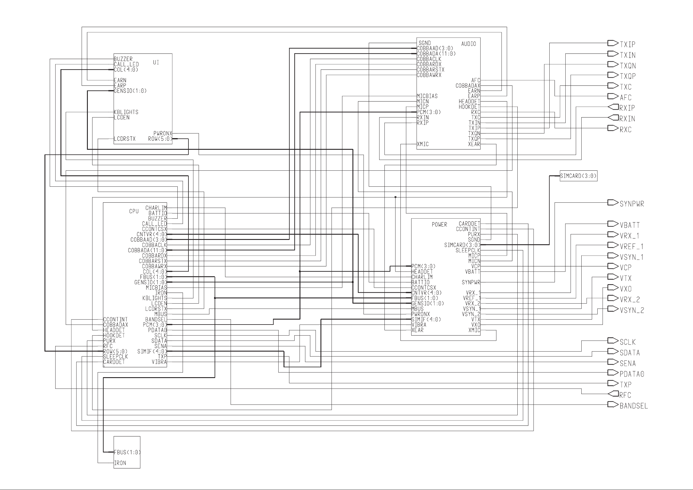
Block Diagram of Baseband (Version 2.1 Edit 98) for layout version 9.1
System Module UG3
NSM–1
Original 10/98
UG3MA/A3–1
Page 2
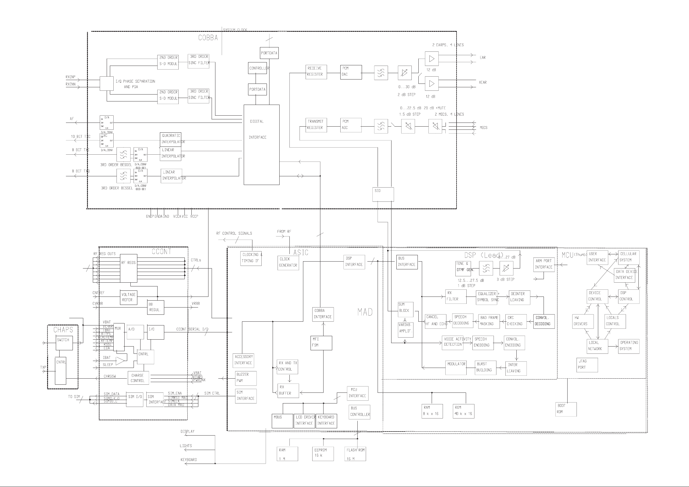
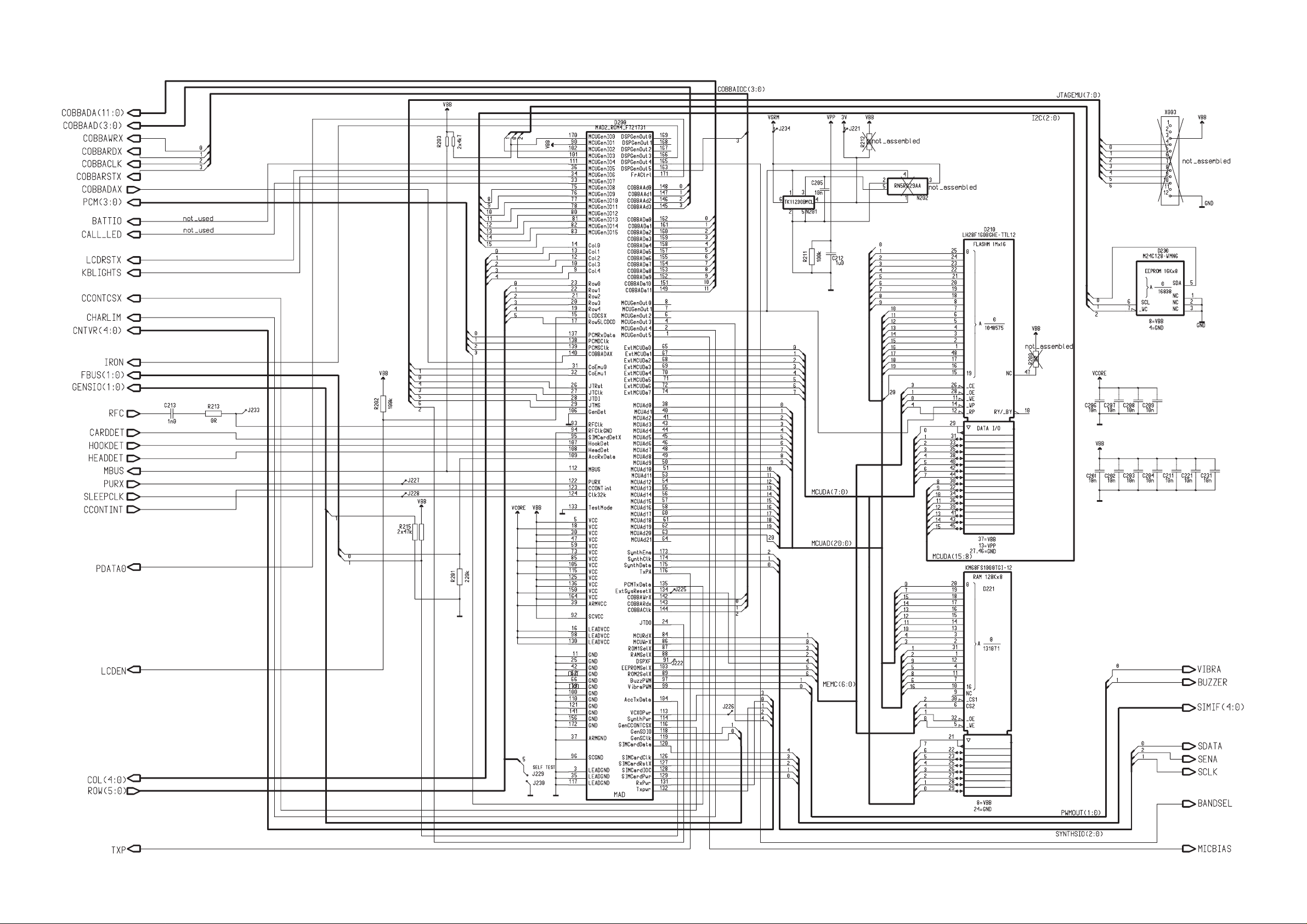
Block Diagram of COBBA, CCONT and MAD
System Module UG3
NSM–1
Original 10/98
UG3MA/A3–2
Page 3
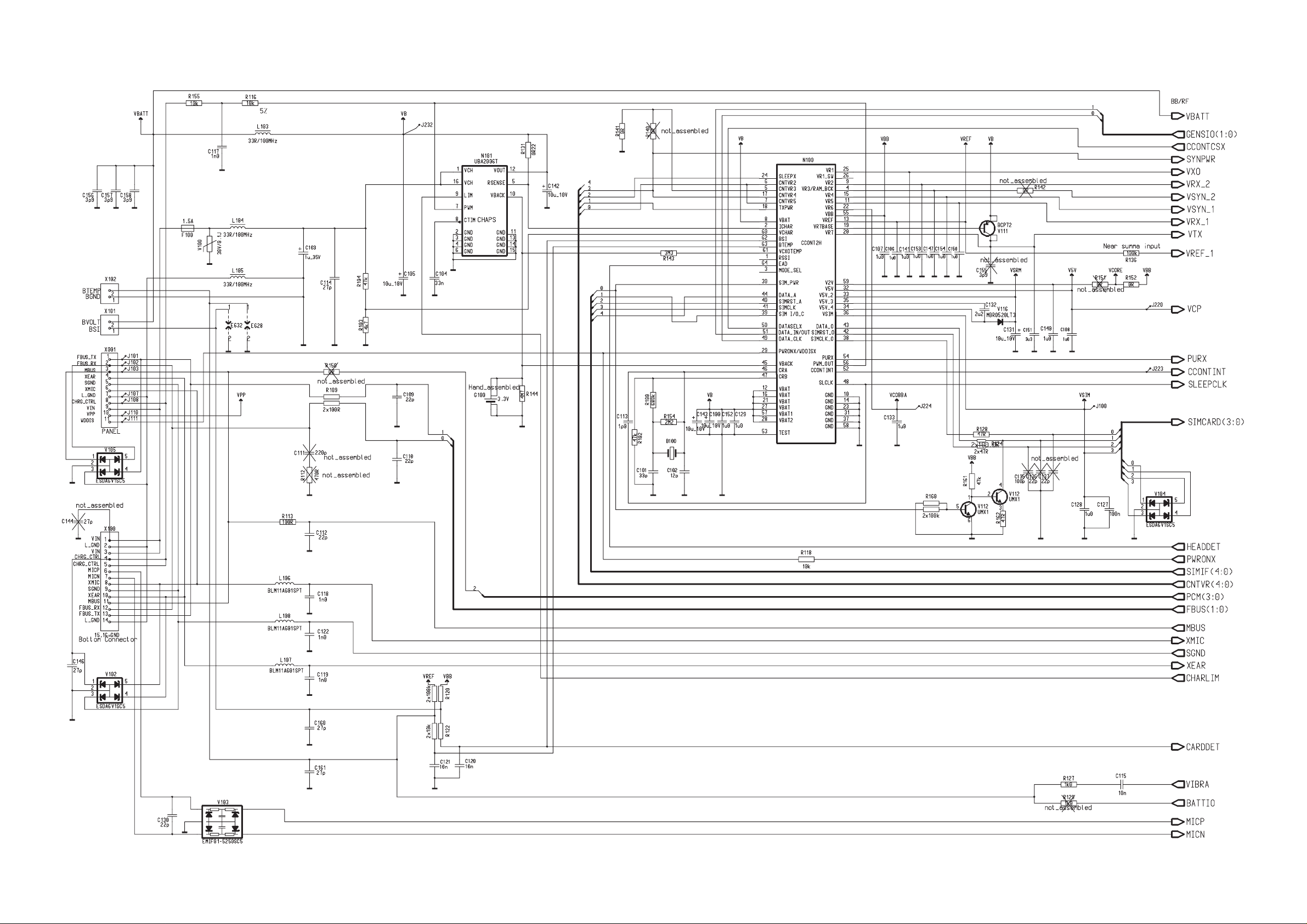
Circuit Diagram of Power Supply (Version 2.31 Edit 299) for layout version 10.4
System Module UG3
NSM–1
Original 10/98
UG3MA/A3–3
Page 4
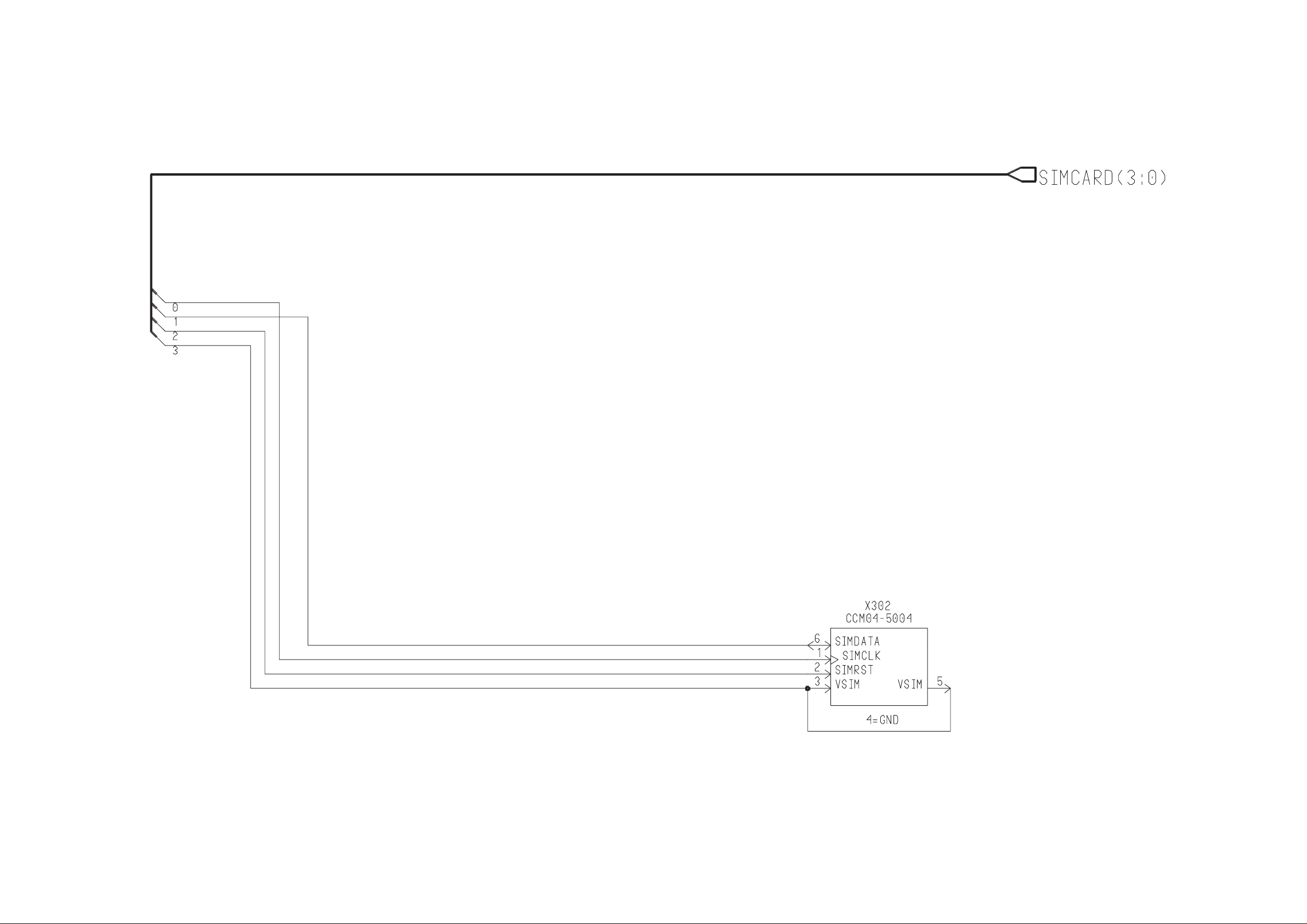
Circuit Diagram of SIM Connector (Version 2.31 Edit 99) for layout version 10.4
System Module UG3
NSM–1
Original 10/98
UG3MA/A3–4
Page 5
Circuit Diagram of CPU Block (Version 2.31 Edit 203) for layout version 10.4
System Module UG3
NSM–1
Original 10/98
UG3MA/A3–5
Page 6
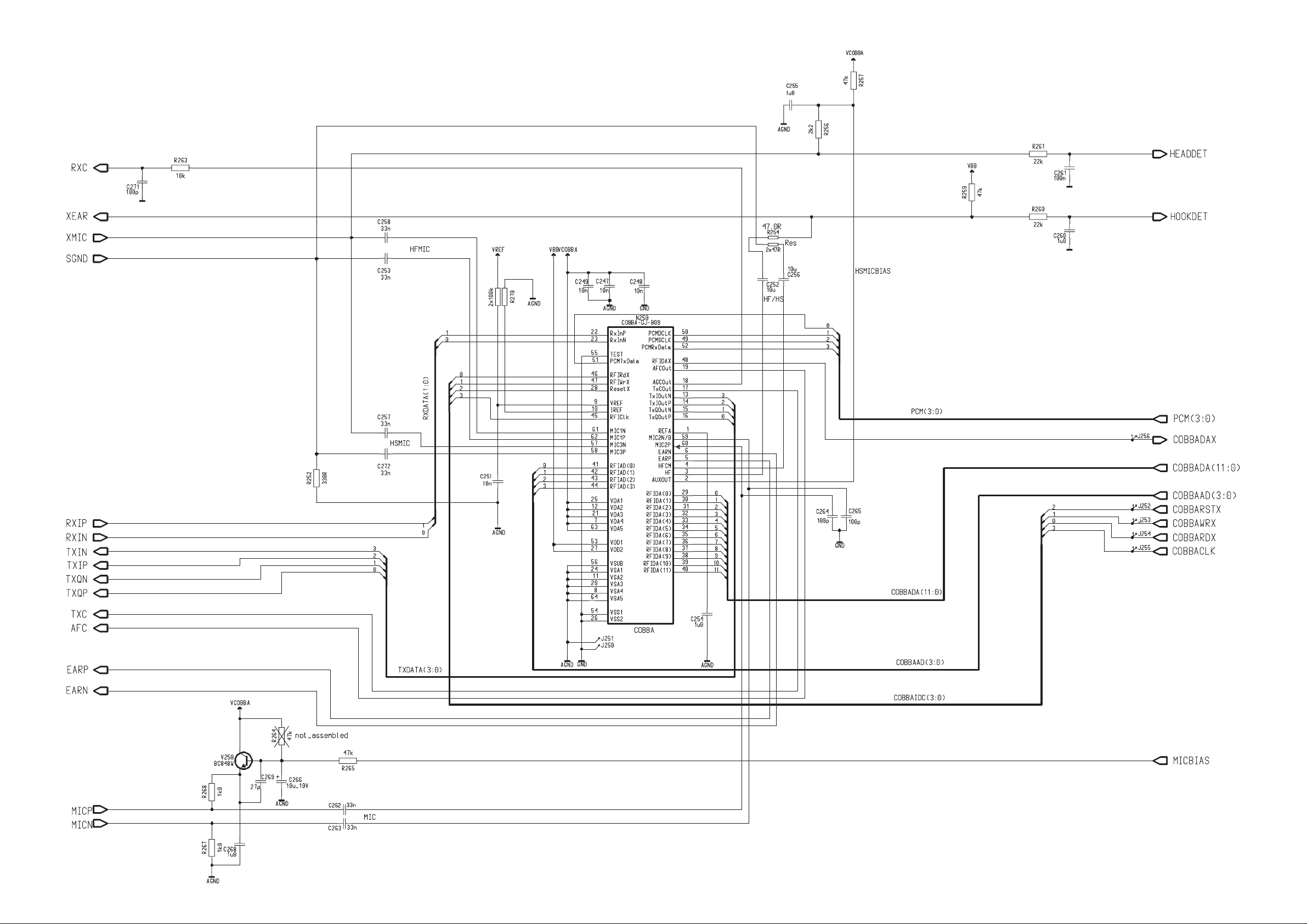
Circuit Diagram of Audio (Version 2.31 Edit 155) for layout version 10.4
System Module UG3
NSM–1
Original 10/98
UG3MA/A3–6
Page 7
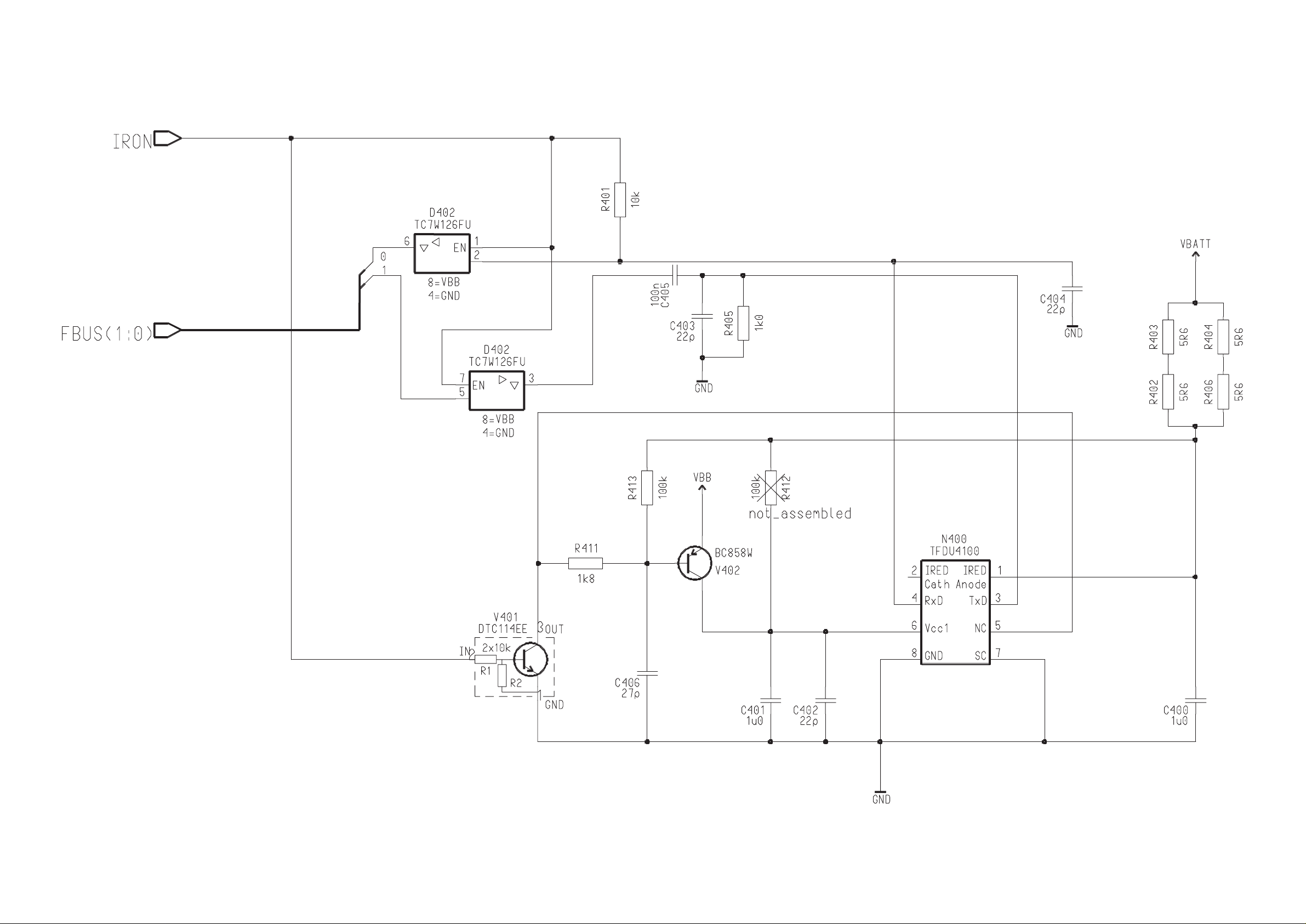
Circuit Diagram of IR Module (Version 2.31 Edit 128) for layout version 10.4
System Module UG3
NSM–1
Original 10/98
UG3MA/A3–7
Page 8

RF Block Diagram
193 MHz 73 MHz
System Module UG3
NSM–1
BAND SELECT
BAND
SELECT
CRFU3
GSM P A
120 MHz
480 MHz
1950 – 2073 MHz
SUMMA
GSM 120 MHz
PCN 240 MHz
60 MHz
Original 10/98
GSM 120 MHz
PCN 240 MHz
PCN P A
UG3MA/A3–8
Page 9
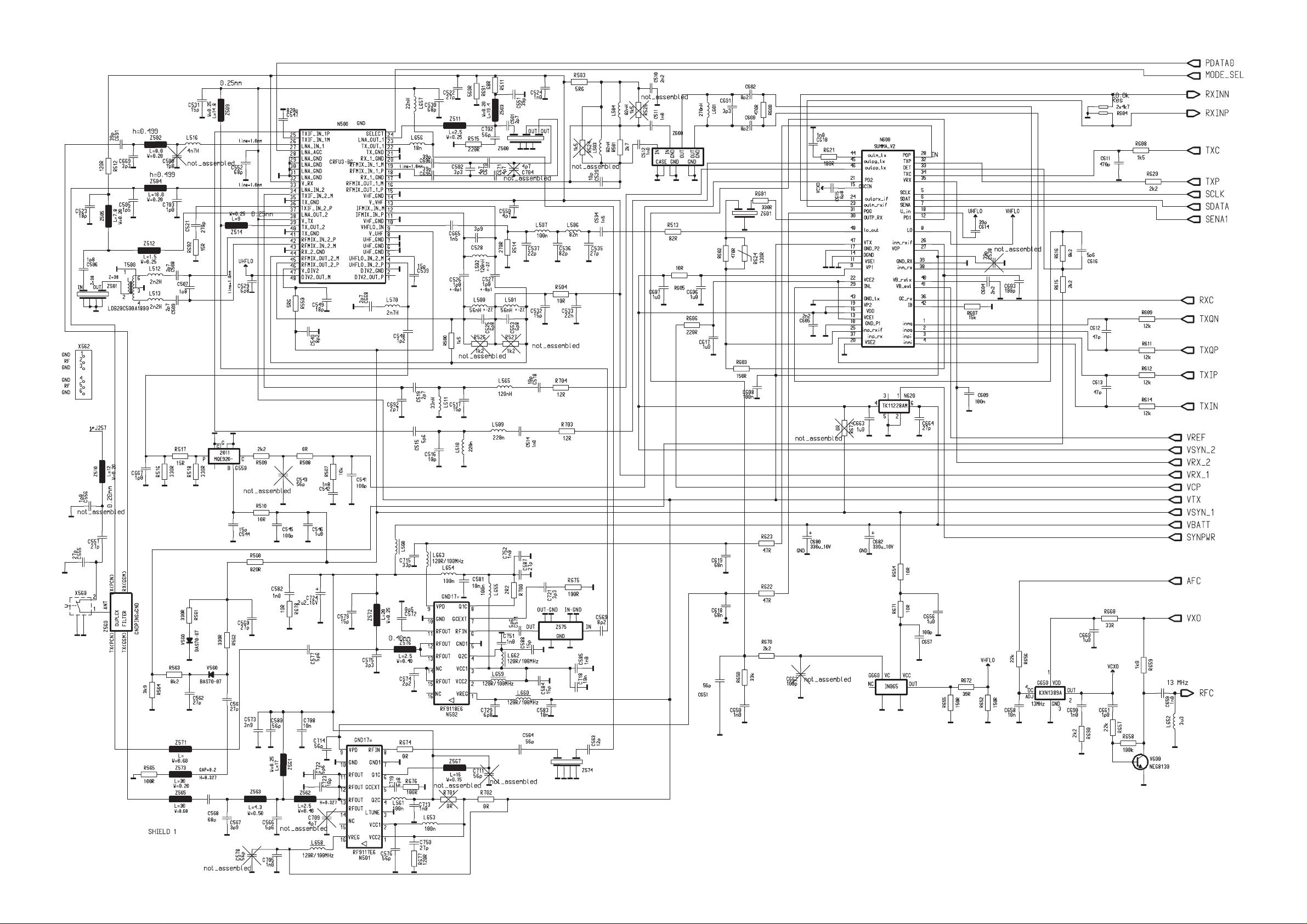
Circuit Diagram of RF Block (Version 2.31 Edit 309) for layout version 10.4
System Module UG3
NSM–1
Original 10/98
UG3MA/A3–9
Page 10

Circuit Diagram of UIF (Version 2.31 Edit 126) for layout version 10.4
System Module UG3
NSM–1
Original 10/98
UG3MA/A3–10
Page 11
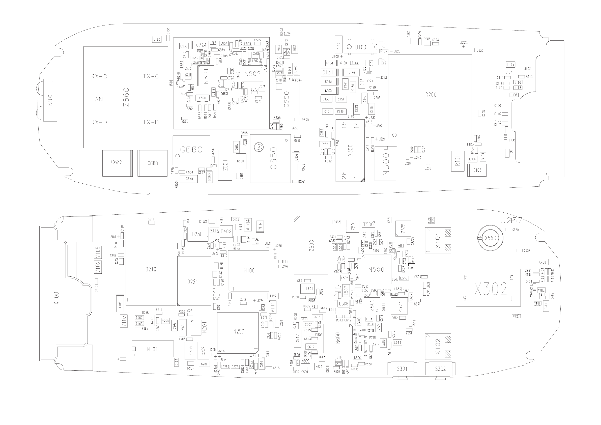
Layout Diagram of UG3MA – Top (Version 10.4)
System Module UG3
NSM–1
Layout Diagram of UG3MA – Bottom (Version 10.4)
Original 10/98
UG3MA/A3–11
Page 12

System Module UG3
testpoint ref name condition dc–level ac–level
J101 FBUS_TX active state pulsed DC (0V72.8V)
J104 CCONTCSX (CCONT chip select) active state pulse active 0V, non–active 2.8V
J108 CHRG_CTRL charger connected pulsed DC (0V/2.8V)
J220 V5V active state nominal 5.0V (min 4.8V, max 5.2V)
J223 CCONTINT (charger, RTC interrupt) interrupt pulse active 2.8V, non–active 0V
J225 EXTSYSRESETX power on reset state 0V, normal state 2.8V
J226 VCXOPWR power on active state 2.8V, non–active 0V
J227 PURX (power on reset) power up/down reset state 0V, normal state 2.8V
J228 SLEEPCLK (32kHz clock) power on pulsed DC (0V/2.8V)
J235 ROM1SELX active state pulse active 0V, non–active 2.8V
J251 AGND pcb ground 0V
J256 COBBADAX active state pulse active 0V, non–active 2.8V
NSM–1
J500 Control voltage for UHF VCO module G600 channel 60
channel 1
channel 124
J504 Control voltage for VHF VCO circuit typ. 2.0 –2.2 V min 0.5 / max 4.0 V
J508 VSYN_2 ( regulated supply for PLLS ) 2.8 V min 2.7 / max 2.85 V
J534&J536 13 MHz IF output to N250 –95 dBm @ X540
(ext. RF connector )
RXC at level of full
calibrated gain
J538 13 MHz output from Z620 to N620 –95 dBm @ X540
(ext. RF connector )
RXC at level of full
calibrated gain
J542 VHF VCO output ( 232 MHz ) – typ. 400 mVpp.
J554 TXC ( TX power control voltage ) @level 19 typ. ca. 0.6 V pulse
J556 TXP ( TX enable ) 2.8 V logic level pulse,
( max. 0.8 V ”0” / min 2.0 V ”1” )
J558 TXQP ( other half of balanced Q–signal ) 0.8 V pulsed 400 mVpp
J560 TXIP ( other half of balanced I–signal ) 0.8 V pulsed 400 mVpp
2.25 +/– 0.25 V
> 0.8 V
< 3.7 V
typ ca. 1.0 – 1.1 V pulsed
min. 0.7 / max. 1.4 V
typ. ca. 1.5 V pulsed typ. ca 600 uVrms
@level 5 typ ca. 1.8 V pulse
typ. 50 mVpp balanced voltage at 13 MHz
> 100 mVpp required
Original 10/98
UG3MA/A3–12
 Loading...