

Page 1

PAMS Technical Documentation
NSC–3 Series Transceivers
Chapter 3
System Module
US4U/US4RM/US4RSMD
Original 11/99
Page 2

NSC–3
PAMS
System Module US4U/US4RM/US4RSMD
CONTENTS
Transceiver NSC–3 3 – 6. . . . . . . . . . . . . . . . . . . . . . . . . . . . . . . . . . . . .
Introduction 3 – 6. . . . . . . . . . . . . . . . . . . . . . . . . . . . . . . . . . . . . . . . . .
Functional Description 3 – 6. . . . . . . . . . . . . . . . . . . . . . . . . . . . . .
Interconnection Diagram 3 – 7. . . . . . . . . . . . . . . . . . . . . . . . . . . . . .
System Module 3 – 8. . . . . . . . . . . . . . . . . . . . . . . . . . . . . . . . . . . . . . . . .
External and Internal Connectors 3 – 8. . . . . . . . . . . . . . . . . . . . .
System Connector Signals 3 – 9. . . . . . . . . . . . . . . . . . . . . . . .
RF–Connector 3 – 9. . . . . . . . . . . . . . . . . . . . . . . . . . . . . . . . . . .
Battery Contacts 3 – 10. . . . . . . . . . . . . . . . . . . . . . . . . . . . . . . . .
Operating Conditions 3 – 10. . . . . . . . . . . . . . . . . . . . . . . . . . . . .
Functional Description 3 – 11. . . . . . . . . . . . . . . . . . . . . . . . . . . . . . . .
Modes of Operation 3 – 11. . . . . . . . . . . . . . . . . . . . . . . . . . . . . . . .
Analog Control Channel (ACCH) Mode 3 – 11. . . . . . . . . . . . . . . .
Analog Voice Channel (AVCH) Mode 3 – 12. . . . . . . . . . . . . . . . .
Digital Control Channel (DCCH) 800 MHz Mode 3 – 12. . . . . . . .
Digital Traffic Channel (DTCH) 800 MHz Mode 3 – 12. . . . . . . . .
Out of Range (OOR) Mode 3 – 13. . . . . . . . . . . . . . . . . . . . . . . . . .
Locals Mode 3 – 13. . . . . . . . . . . . . . . . . . . . . . . . . . . . . . . . . . . . . . .
Power Distribution Diagram 3 – 14. . . . . . . . . . . . . . . . . . . . . . . . . .
External interfaces 3 – 15. . . . . . . . . . . . . . . . . . . . . . . . . . . . . . . . . . . .
Signals between baseband and User Interface section 3 – 15. .
User Interface module connection 3 – 15. . . . . . . . . . . . . . . . . . . .
Earphone 3 – 15. . . . . . . . . . . . . . . . . . . . . . . . . . . . . . . . . . . . . . . . .
Buzzer 3 – 15. . . . . . . . . . . . . . . . . . . . . . . . . . . . . . . . . . . . . . . . . . . .
Baseband Module 3 – 16. . . . . . . . . . . . . . . . . . . . . . . . . . . . . . . . . . . .
Power Distribution 3 – 16. . . . . . . . . . . . . . . . . . . . . . . . . . . . . . . . . . . .
Charging Control 3 – 17. . . . . . . . . . . . . . . . . . . . . . . . . . . . . . . . . . .
2–wire charging 3 – 17. . . . . . . . . . . . . . . . . . . . . . . . . . . . . . . . . . . .
3–wire charging 3 – 18. . . . . . . . . . . . . . . . . . . . . . . . . . . . . . . . . . . .
Watchdog 3 – 18. . . . . . . . . . . . . . . . . . . . . . . . . . . . . . . . . . . . . . . . .
Power up 3 – 19. . . . . . . . . . . . . . . . . . . . . . . . . . . . . . . . . . . . . . . . .
Power up when power–button is pushed 3 – 19. . . . . . . . . . . . . .
IBI (Intelligent Battery Interface) 3 – 20. . . . . . . . . . . . . . . . . . . . . .
Mixed trigger to power up 3 – 20. . . . . . . . . . . . . . . . . . . . . . . . . . .
Power Off 3 – 20. . . . . . . . . . . . . . . . . . . . . . . . . . . . . . . . . . . . . . . . .
Power off by pushing Power–key 3 – 20. . . . . . . . . . . . . . . . . . . . .
Power off when battery voltage low 3 – 21. . . . . . . . . . . . . . . . . . .
Power off when fault in the transmitter 3 – 21. . . . . . . . . . . . . . . .
Sleep Mode 3 – 21. . . . . . . . . . . . . . . . . . . . . . . . . . . . . . . . . . . . . . .
Waking up from the Sleep–mode 3 – 21. . . . . . . . . . . . . . . . . . . . .
Baseband submodules 3 – 22. . . . . . . . . . . . . . . . . . . . . . . . . . . . . . . .
Technical Documentation
Page No
Page 3 – 2
Original 11/99
Page 3

PAMS
NSC–3
Technical Documentation
CTRLU 3 – 22. . . . . . . . . . . . . . . . . . . . . . . . . . . . . . . . . . . . . . . . . . .
MCU main features 3 – 22. . . . . . . . . . . . . . . . . . . . . . . . . . . . . . . . .
DSP main features 3 – 23. . . . . . . . . . . . . . . . . . . . . . . . . . . . . . . . .
System Logic main features 3 – 23. . . . . . . . . . . . . . . . . . . . . . . . .
Memories 3 – 23. . . . . . . . . . . . . . . . . . . . . . . . . . . . . . . . . . . . . . . . .
AUDIO–RF 3 – 24. . . . . . . . . . . . . . . . . . . . . . . . . . . . . . . . . . . . . . . .
Cobba main features 3 – 24. . . . . . . . . . . . . . . . . . . . . . . . . . . . . . .
Speech processing 3 – 25. . . . . . . . . . . . . . . . . . . . . . . . . . . . . . . . .
Alert Signal Generation 3 – 25. . . . . . . . . . . . . . . . . . . . . . . . . . . . .
PWRU 3 – 26. . . . . . . . . . . . . . . . . . . . . . . . . . . . . . . . . . . . . . . . . . . .
CCONT main features 3 – 26. . . . . . . . . . . . . . . . . . . . . . . . . . . . . .
CHAPS main features 3 – 26. . . . . . . . . . . . . . . . . . . . . . . . . . . . . .
RF Module 3 – 27. . . . . . . . . . . . . . . . . . . . . . . . . . . . . . . . . . . . . . . . . .
RF Frequency Plan 3 – 27. . . . . . . . . . . . . . . . . . . . . . . . . . . . . . . . .
DC Characteristics 3 – 27. . . . . . . . . . . . . . . . . . . . . . . . . . . . . . . . .
Power Distribution Diagram 3 – 27. . . . . . . . . . . . . . . . . . . . . . . . . .
Power Distribution – Typical Currents 3 – 29. . . . . . . . . . . . . . . . .
Functional Description 3 – 30. . . . . . . . . . . . . . . . . . . . . . . . . . . . . .
Receiver 3 – 30. . . . . . . . . . . . . . . . . . . . . . . . . . . . . . . . . . . . . . . . . .
DAMPS800 RX 3 – 30. . . . . . . . . . . . . . . . . . . . . . . . . . . . . . . . . . . .
Transmitter 3 – 31. . . . . . . . . . . . . . . . . . . . . . . . . . . . . . . . . . . . . . . .
DAMPS800 TX 3 – 31. . . . . . . . . . . . . . . . . . . . . . . . . . . . . . . . . . . .
Frequency Synthesizers 3 – 31. . . . . . . . . . . . . . . . . . . . . . . . . . . .
DAMPS800 operation 3 – 32. . . . . . . . . . . . . . . . . . . . . . . . . . . . . . .
Supply voltages in different modes of operation 3 – 32. . . . . . . .
Software Compensations 3 – 33. . . . . . . . . . . . . . . . . . . . . . . . . . . .
Power Levels (TXC) vs. Temperature 3 – 33. . . . . . . . . . . . . . .
Power Levels (TXC) vs. Channel 3 – 33. . . . . . . . . . . . . . . . . . .
Power levels vs. Battery Voltage 3 – 33. . . . . . . . . . . . . . . . . . .
TX Power Up/Down Ramps 3 – 33. . . . . . . . . . . . . . . . . . . . . . .
Modulator Output Level 3 – 33. . . . . . . . . . . . . . . . . . . . . . . . . . .
Digital Mode RSSI 3 – 33. . . . . . . . . . . . . . . . . . . . . . . . . . . . . . .
RF Block Specifications 3 – 34. . . . . . . . . . . . . . . . . . . . . . . . . . . . . . .
Receiver 3 – 34. . . . . . . . . . . . . . . . . . . . . . . . . . . . . . . . . . . . . . . . . .
DAMPS 800 Mhz Front End 3 – 34. . . . . . . . . . . . . . . . . . . . . . . . .
First IF Filter 3 – 34. . . . . . . . . . . . . . . . . . . . . . . . . . . . . . . . . . . . . . .
Transmitter 3 – 35. . . . . . . . . . . . . . . . . . . . . . . . . . . . . . . . . . . . . . . .
RF Characteristics 3 – 35. . . . . . . . . . . . . . . . . . . . . . . . . . . . . . . . .
Power Levels 3 – 35. . . . . . . . . . . . . . . . . . . . . . . . . . . . . . . . . . . . . .
Synthesizers 3 – 35. . . . . . . . . . . . . . . . . . . . . . . . . . . . . . . . . . . . . .
UHF 3 – 35. . . . . . . . . . . . . . . . . . . . . . . . . . . . . . . . . . . . . . . . . . . . . .
VHF 3 – 36. . . . . . . . . . . . . . . . . . . . . . . . . . . . . . . . . . . . . . . . . . . . . .
Output Levels 3 – 36. . . . . . . . . . . . . . . . . . . . . . . . . . . . . . . . . . . . . .
Connections 3 – 37. . . . . . . . . . . . . . . . . . . . . . . . . . . . . . . . . . . . . . . . .
RF–Baseband signals 3 – 37. . . . . . . . . . . . . . . . . . . . . . . . . . . . . .
System Module US4U/US4RM/US4RSMD
Original 11/99
Page 3 – 3
Page 4

NSC–3
PAMS
System Module US4U/US4RM/US4RSMD
Data Interface and Timing 3 – 43. . . . . . . . . . . . . . . . . . . . . . . . . . .
Digital control channels 3 – 44. . . . . . . . . . . . . . . . . . . . . . . . . . .
Analog control channel 3 – 45. . . . . . . . . . . . . . . . . . . . . . . . . . .
Parts list of US4U (EDMS Issue 8.3) Code: 0200973 3 – 46. . . . . . . .
Parts list of US4RM (EDMS Issue 3.2) Code: 0201308 3 – 55. . . . . .
Parts list of US4RSMD (EDMS Issue 3.0) Code: 0201371 3 – 64. . .
Schematic Diagrams: US4U
Circuit Diagram of System Blocks (Version 16 Edit 188) layout 16 3/A3–1
Circuit Diagram of Power Supply (Version 16 Edit 286) layout 16 3/A3–2
Circuit Diagram of CTRLU Block (Version 16 Edit 287) layout 16 3/A3–3
Circuit Diagram of Audio (Version 16 Edit 213) for layout version 16 3/A3–4
Circuit Diagram of Transmitter (Version 16 Edit 549) layout 16 3/A3–5
Technical Documentation
Circuit Diagram of Receiver (Version 16 Edit 129) for layout version 16 3/A3–6
Circuit Diagram of Synthesizer (Version 16 Edit 156) for layout 16 3/A3–7
Circuit Diagram of RF Block (Version 16 Edit 104) for layout version 16 3/A3–8
Circuit Diagram of RF–BB Interface (Version 16 Edit 70) layout 16 3/A3–9
Layout Diagram of US4U (Layout version 16) 3/A3–10. . . . . . . . . . . . . .
Schematic Diagrams: US4RM
Circuit Diagram of System Blocks (Version 05.03 Edit 2) layout 5 3/A3–1
Circuit Diagram of Power Supply (Version 05.01 Edit 4) layout 5 3/A3–2
Circuit Diagram of CTRLU Block (Version 05.01 Edit 4) layout 5 3/A3–3
Circuit Diagram of Audio (Version 06.01 Edit 3) for layout version 5 3/A3–4
Circuit Diagram of Transmitter (Version 05.01 Edit 2) layout 5 3/A3–5
Circuit Diagram of Receiver (Version 05.01 Edit 2) for layout version 5 3/A3–6
Circuit Diagram of Synthesizer (Version 05.01 Edit 2) for layout 5 3/A3–7
Circuit Diagram of RF Block (Version 06.01 Edit 2) for layout version 5 3/A3–8
Circuit Diagram of RF–BB Interface (Version 06.01 Edit 3) layout 5 3/A3–9
Layout Diagram 1/2 of US4RM (Layout version 5) 3/A3–10. . . . . . . . . . .
Layout Diagram 2/2 of US4RM (Layout version 5) 3/A3–11. . . . . . . . . . .
Page 3 – 4
Original 11/99
Page 5

PAMS
NSC–3
Technical Documentation
Schematic Diagrams: US4RSMD
Circuit Diagram of System Blocks (Version 06.41 Edit 9) 3/A3–1
Circuit Diagram of Power Supply (Version 06.41 Edit 8) 3/A3–2
Circuit Diagram of CTRLU Block (Version 06.41 Edit 7) 3/A3–3
Circuit Diagram of Audio (Version 06.41 Edit 7) 3/A3–4
Circuit Diagram of Transmitter (Version 06.41 Edit 11) 3/A3–5
Circuit Diagram of Receiver (Version 06.41 Edit 11) 3/A3–6
Circuit Diagram of Synthesizer (Version 06.41 Edit 8) 3/A3–7
Circuit Diagram of RF Block (Version 06.41 Edit 6) 3/A3–8
Circuit Diagram of RF–BB Interface (Version 06.41 Edit 11) 3/A3–9
Layout Diagram 1/2 of US4RSMD (Phase 3) 3/A3–10. . . . . . . . . . . . . . .
Layout Diagram 2/2 of US4RSMD (Phase 3) 3/A3–11. . . . . . . . . . . . . . .
System Module US4U/US4RM/US4RSMD
Original 11/99
Page 3 – 5
Page 6

NSC–3
PAMS
System Module US4U/US4RM/US4RSMD
Transceiver NSC–3
Introduction
The NSC–3 is a radio transceiver unit for the TDMA 800 networks. The
transceiver is true 3 V transceiver.
The transceiver consists of System/RF module ( US4U Phase1, US4RM
Phase 2 and US4RSMD Phase 3), User interface module ( UE4 ) and assembly parts.
The purpose of the baseband module is to control the phone and process
audio signals to and from RF. The module also controls the user interface.
The transceiver has full graphic display and two soft key based user interface.
The antenna is a fixed helix. External antenna connection is provided by
rear RF connector
Technical Documentation
Functional Description
There are five different operation modes:
– power off mode
– sleep mode
– active mode
– charge mode
– local mode
In the power off mode only the circuits needed for power up are supplied.
In the idle mode circuits are powered down and only sleep clock is run-
ning.
In the active mode all the circuits are supplied with power although some
parts might be in the idle state part of the time.
The charge mode is effective in parallel with all previous modes. The
charge mode itself consists of two different states, i.e. the charge and the
maintenance mode.
The local mode is used for alignment and testing.
Page 3 – 6
Original 11/99
Page 7
PAMS
NSC–3
Technical Documentation
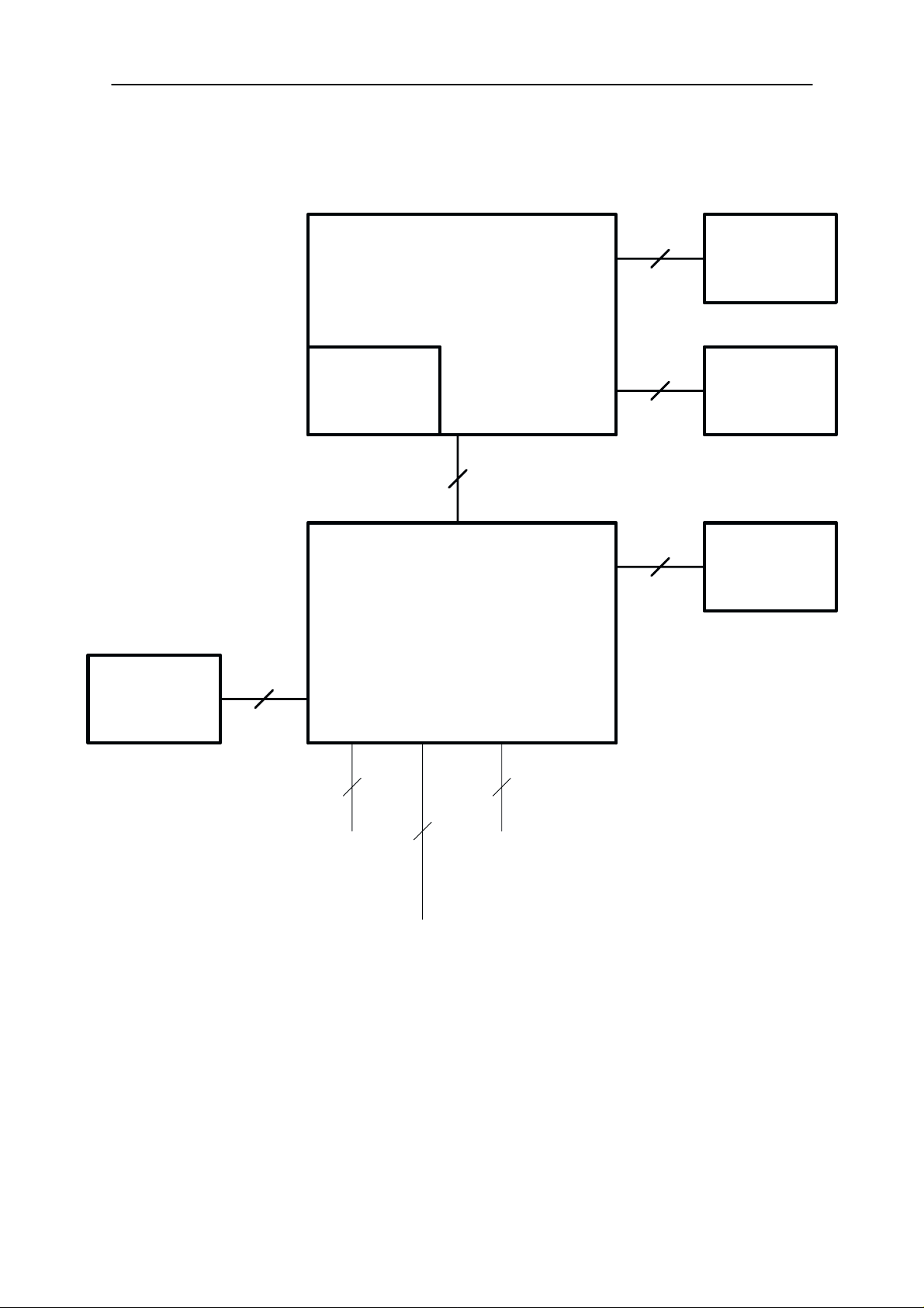
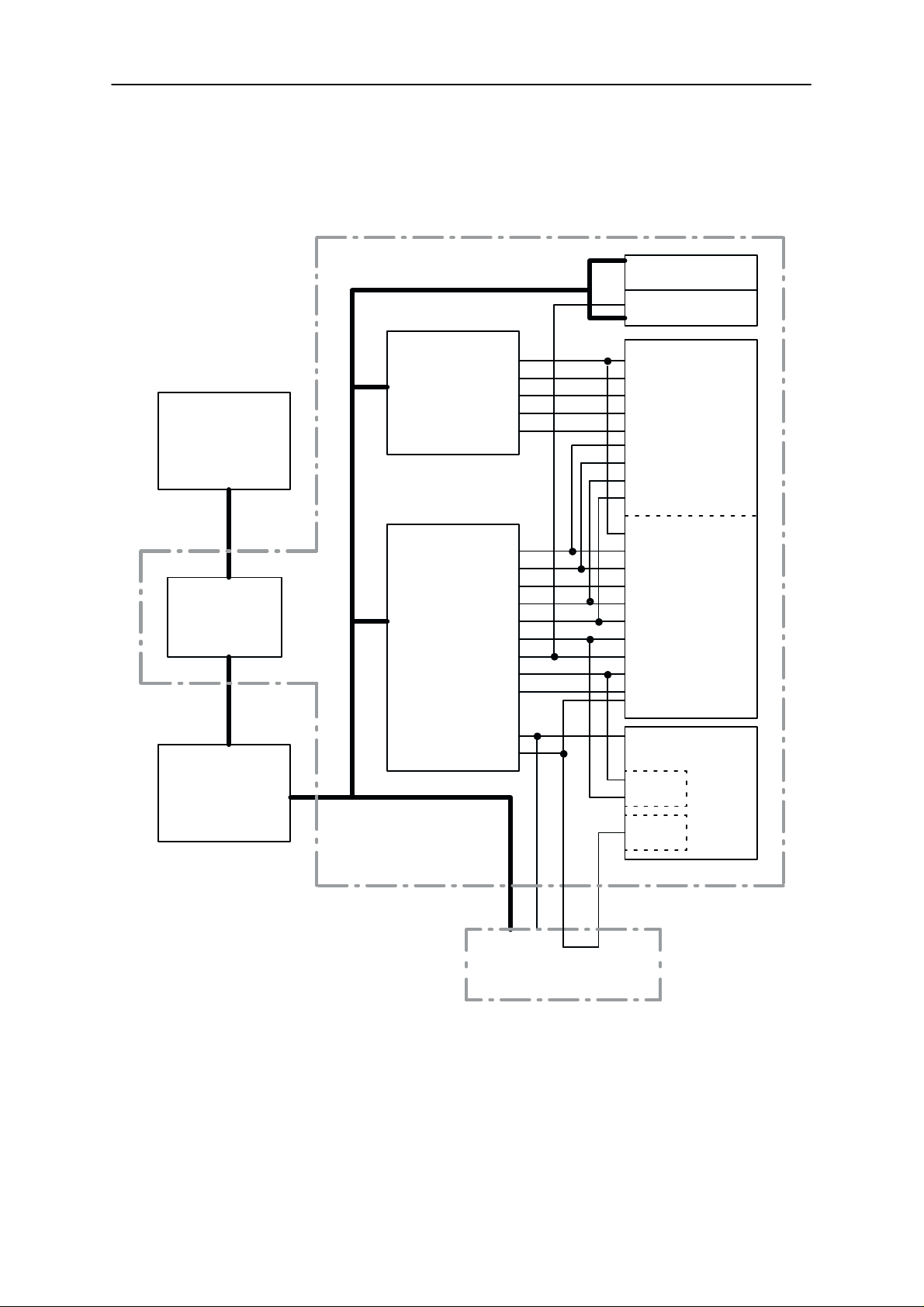
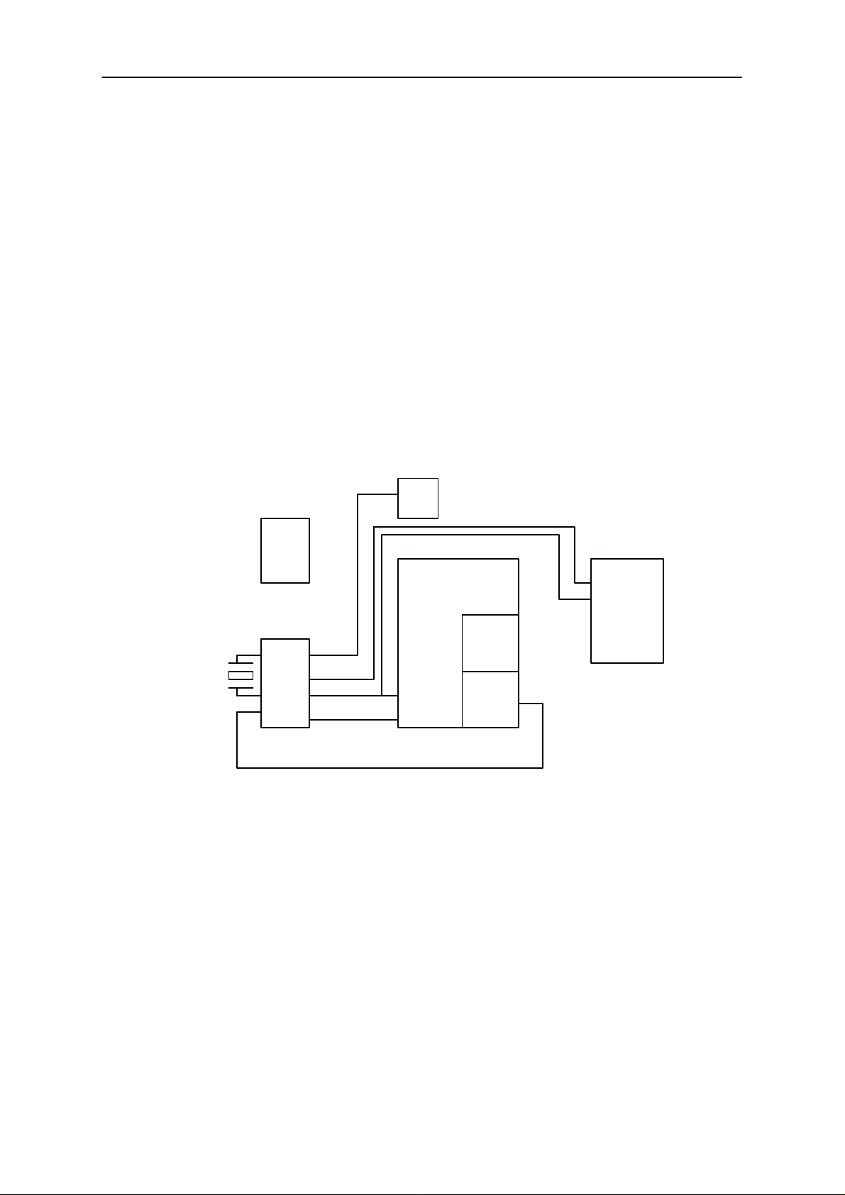
Interconnection Diagram
User Interface
Module
Keypad
System Module US4U/US4RM/US4RSMD
9
Display
UE4
2
Earpiece
28
4
Antenna
1
(including Mic)
US4U/US4RM/
System
Connector
Connector
Battery
System/RF
Module
US4RSMD
3 + 36+2
2
Charger
RF
Original 11/99
Page 3 – 7
Page 8
NSC–3
PAMS
System Module US4U/US4RM/US4RSMD
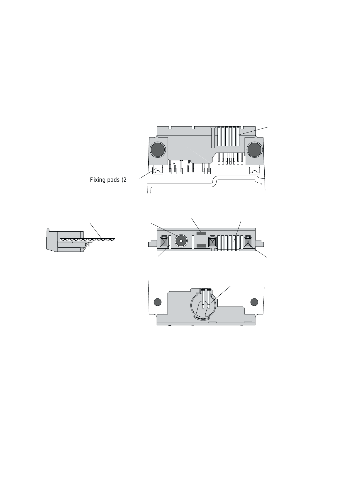
System Module
External and Internal Connectors
B side view
Fixing pads (2 pcs)
Engine PCB
DC Jack
1
Microphone
acoustic ports
Technical Documentation
IBI connector
(6 pads)
8
7
14
Bottom
connector (6 pads)
A side view
Charger pads (3 pcs)
Cable locking holes (3 pcs)
Cavity for microphone
Page 3 – 8
Original 11/99
Page 9
PAMS
NSC–3
Technical Documentation
System Module US4U/US4RM/US4RSMD
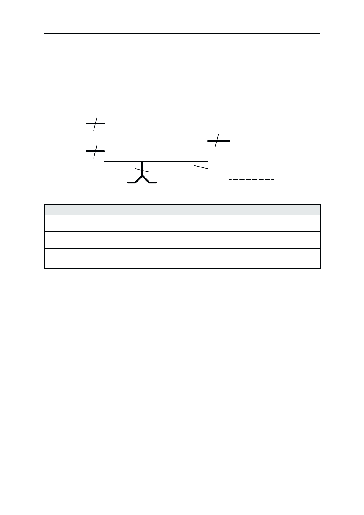
System Connector Signals
Pin Name Function Description
1 V_IN Bottom charger contacts Charging voltage.
2 L_GND DC Jack Logic and charging ground.
3 V_IN DC Jack Charging voltage.
4 CHRG_CTRL DC Jack Charger control.
5 CHRG_CTRL Bottom charger contacts Charger control.
6 MICP Microphone Microphone signal, positive node.
7 MICN Microphone Microphone signal, negative node.
8 XMIC Bottom & IBI connectors Analog audio input.
9 SGND Bottom & IBI connectors Audio signal ground.
10 XEAR Bottom & IBI connectors Analog audio output.
11 MBUS Bottom & IBI connectors Bidirectional serial bus.
12 FBUS_RX Bottom & IBI connectors Serial data in.
13 FBUS_TX Bottom & IBI connectors Serial data out.
14 L_GND Bottom charger contacts Logic and charging ground.
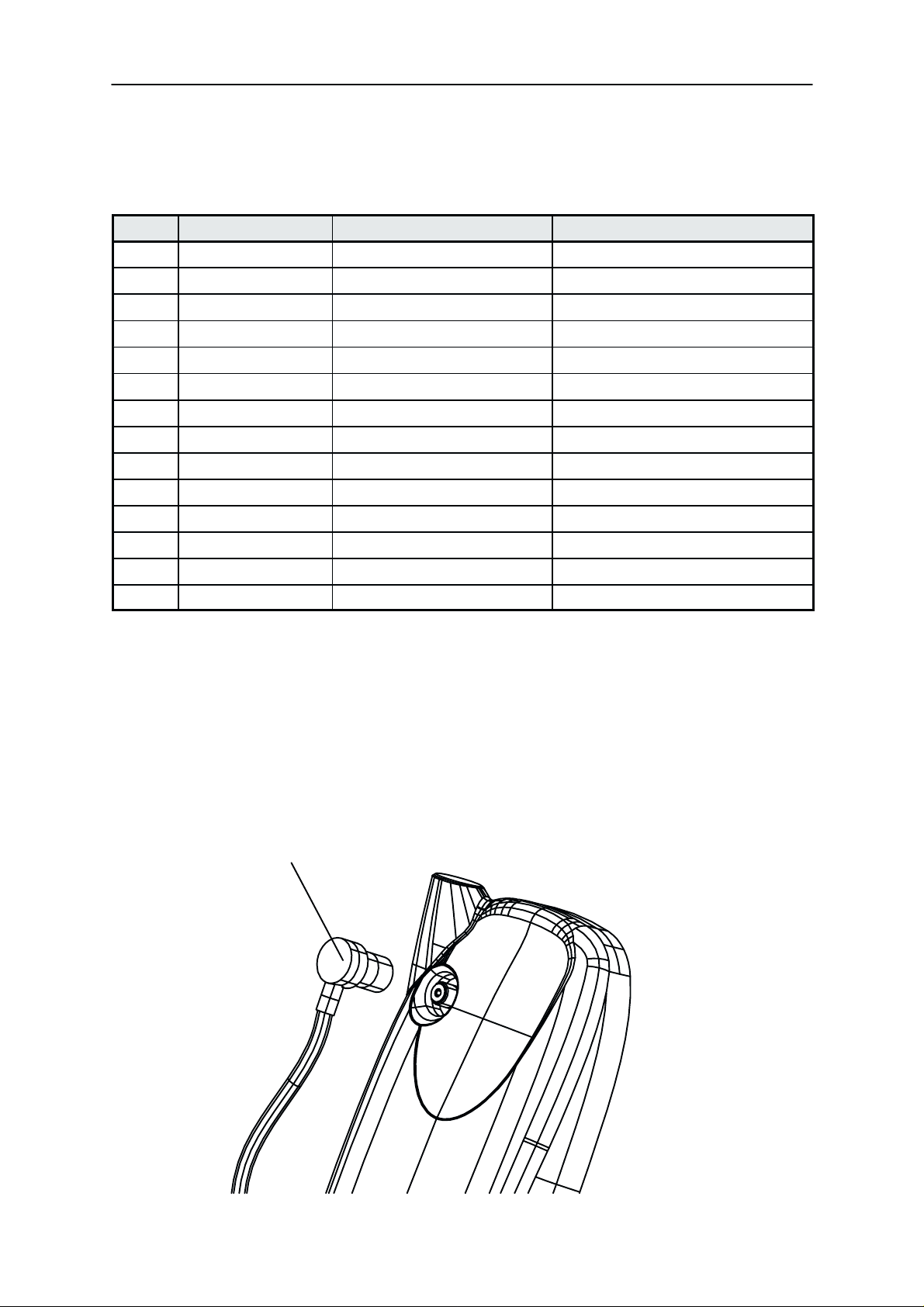
RF–Connector
The RF–connector is needed to utilize the external antenna with Car
Cradle. The RF–connector is located on the back side of the transceiver
on the top section. The connector is plug type connector with special mechanical switching.
Accessory side of connector
Part will be floating in
car holder
Phone side of connector
Original 11/99
Page 3 – 9
Page 10
NSC–3
PAMS
System Module US4U/US4RM/US4RSMD
Technical Documentation
Battery Contacts
Pin Name Function Description
1 BVOLT Battery voltage Battery voltage
2 BSI Battery Size Indicator Input voltage
3 BTEMP Battery temperature indication
Phone power up
Battery power up
PWM to VIBRA BA TTERY
4 BGND Ground
Input voltage
Input voltage
Output voltage
PWM output signal frequency
Operating Conditions
Environmental condition Ambient temperature Notes
Normal operation conditions +7 oC ... +40 oC Specifications fulfilled and fast
charging possible
Extreme operation conditions –10 oC ... +55 oC Specifications fulfilled
Reduced performance condi-
tions
Intermittent operation condi-
tions
Cessation of operation <–25 oC and >80 oC No storage or operation attempt
Long term storage conditions 0 oC ... +40 oC Battery only up to +30 oC !
Short term storage, max. 96 h –25 oC ... +70 oC Cumulative for life–time of bat-
Short term storage, max. 12 h –25 oC ... +80 oC Cumulative for life–time of bat-
–25 oC ... +75 oC LCD operation
Short term operation > +70 oC
+55 oC ... +65 oC Operational only for short peri-
ods
–25 oC ... –10 oC and
+65
o
C ... +80 oC
Operation maybe not possible
but attempt to operate will not
damage the phone
possible without permanent
damage
tery
tery
Page 3 – 10
Original 11/99
Page 11

PAMS
NSC–3
Technical Documentation
Functional Description
The US4U (Phase 1) / US4RM (Phase 2) / US4RSMSD (Phase 3) engine
consist of a Baseband/RF module with connections to a separate User
Interface module. Baseband and RF submodules are interconnected with
PCB wiring. The engine can be connected to accessories via bottom system
connector and an Intelligent Battery Interface (IBI) connector.
The RF submodule receives and demodulates radio frequency signals from
the base station and transmits modulated RF signals to the base station. It
consists of functional submodules Receiver, Frequency Synthesizer and
Transmitter . The RF submodule can further be devided into lower band and
upper band functions.
The Baseband module containes audio, control, signal processing and
power supply functions. It consists of functional submodules CTRLU
(Control Unit; MCU, DSP, logic and memories), PWRU (Power Supply;
regulators and charging) and AUDIO_RF (audio coding, RF–BB interface).
System Module US4U/US4RM/US4RSMD
Modes of Operation
US4U/US4RM/US4RSMD operates in five cellular modes and a local mode
for service:
– Analog Control Channel (ACCH) 800 MHz Mode,
– Analog Voice Channel (AVCH) 800 MHz Mode,
– Digital Control Channel (DCCH) 800 MHz Mode,
– Digital Traffic Channel (DTCH) 800 MHz Mode,
– Out of Range (OOR) Mode,
– Locals mode, used by Production and After Sales.
Analog Control Channel (ACCH) Mode
On analog control channel the phone receives continuous signalling
messages on Forward Control Channel (FOCC) from the base station, being
most of the time in IDLE mode. Only the receiver part is on. The phone scans
the preferred dedicated control channels to find and lock to the strongest
channel for reading information from this control channel.
DSP is not used on ACCH (it stays in sleep mode), except during channel
scanning for loading the synthesizers.
As a separate sleep clock is used, also the VCTCXO can be turned off
periodically with the RF parts. Only the sleep clock and necessary timers in
MCU are operational.
When registration is demanded the phone sends (TX on) it’s information on
Reverse Control Channel (RECC) to the base station. The phone’s location
is updated in the switching office.
Original 11/99
Page 3 – 11
Page 12

NSC–3
PAMS
System Module US4U/US4RM/US4RSMD
If a call is initiated, either by the user or the base station, the phone moves
to the allocated analog voice channel or digital traffic channel depending on
the orders by the base station.
Analog Voice Channel (AVCH) Mode
The phone receives and transmits analog audio signal. All circuitry is
powered on (except the receiver parts used only in digital modes). DSP does
the audio processing and in Hands Free mode also performs
echo–cancellation and HF algorithms. The COBBA IC makes A/D
conversion for the MIC signal, and D/A conversion for the EAR signal.
With audio signal also the Supervisory Audio Tone (SAT) is being received
from the base station. The SA T frequency can be 5970 Hz, 6000Hz or 6030
Hz, defined by the base station. The DSP phase lock loop locks to the SA T,
detects if the frequency is the expected one and examines the signal quality .
DSP reports SAT quality figures regularily to the MCU. The received SAT
signal is transmitted back (transponded) to the base station.
Technical Documentation
The base station can send signalling messages on Forward Voice Channel
(FVC) to the phone, by replacing the audio with a burst of Wide Band Data
(WBD). These are typically hand–off or power level messages. The RX
modem in System Logic receives the signalling message burst and gives an
interrupt to the MCU for reading the data. MCU gives a message to DSP to
mute the audio path during the burst. MCU can acknowledge the messages
on Reverse V oice Channel (RVC), where DSP sends the WBD to transmitter
RF.
Digital Control Channel (DCCH) 800 MHz Mode
On digital control channel (DCCH) DSP receives the paging information from
the Paging channels and sends the messages to MCU for processing.
Each Hyperframe (HFC) comprises two Superframes (SF), the Primary (p)
and the Secondary (s) paging frame. The assigned Page Frame Class (PFC)
defines the frames which must be received, and thus defines when the
receiver must be on.
The phone is in sleep mode between the received time slots. The sleep clock
timer is set and MCU, DSP and RF parts (including VCTCXO) are powered
down. Only sleep clock and the respective timers are running.
From DCCH phone may be ordered to analog control channel or to analog
or digital traffic channel.
Digital Traffic Channel (DTCH) 800 MHz Mode
Digital Voice Channel (S–DTCH)
On digital voice channel DSP processes the speech signal in 20 ms time
slots. DSP performs the speech and channel functions in time shared
fashion and is in sleep mode whenever possible. RX and TX parts are
Page 3 – 12
Original 11/99
Page 13

PAMS
NSC–3
Technical Documentation
powered on and off according to the slot timing. MCU is waken up mainly
by DSP, when there is signalling information for the Cellular Software.
Digital Data Channel (D–DTCH)
In Digital Data Channel Mode audio processing is not needed and audio
circuitry can be shut down. Otherwise the mode is similar to Digital Voice
Channel Mode.
Out of Range (OOR) Mode
If the phone can’t find signal from the base station on any control channel
(analog or digital) it can go into OOR mode for power saving. All RF circuits
are powered down and the baseband circuits in a low power mode, VCTCXO
stopped and only the sleep clock running. After a programmable timer in
MCU has elapsed the phone turns the receiver on and tries to receive
signalling data from base station. If it succeeds, the phone goes to standby
mode on analog or digital control channel. If the connection can not be
established the phone returns to OOR mode until the timer elapses again.
System Module US4U/US4RM/US4RSMD
Locals Mode
Locals mode is used for testing purposes by Product Development,
Production and After Sales. The Cellular Software is stopped (no signalling
to base station), and the phone is controlled by MBUS/FBUS messages by
the controlling PC.
Original 11/99
Page 3 – 13
Page 14
NSC–3
PAMS
System Module US4U/US4RM/US4RSMD
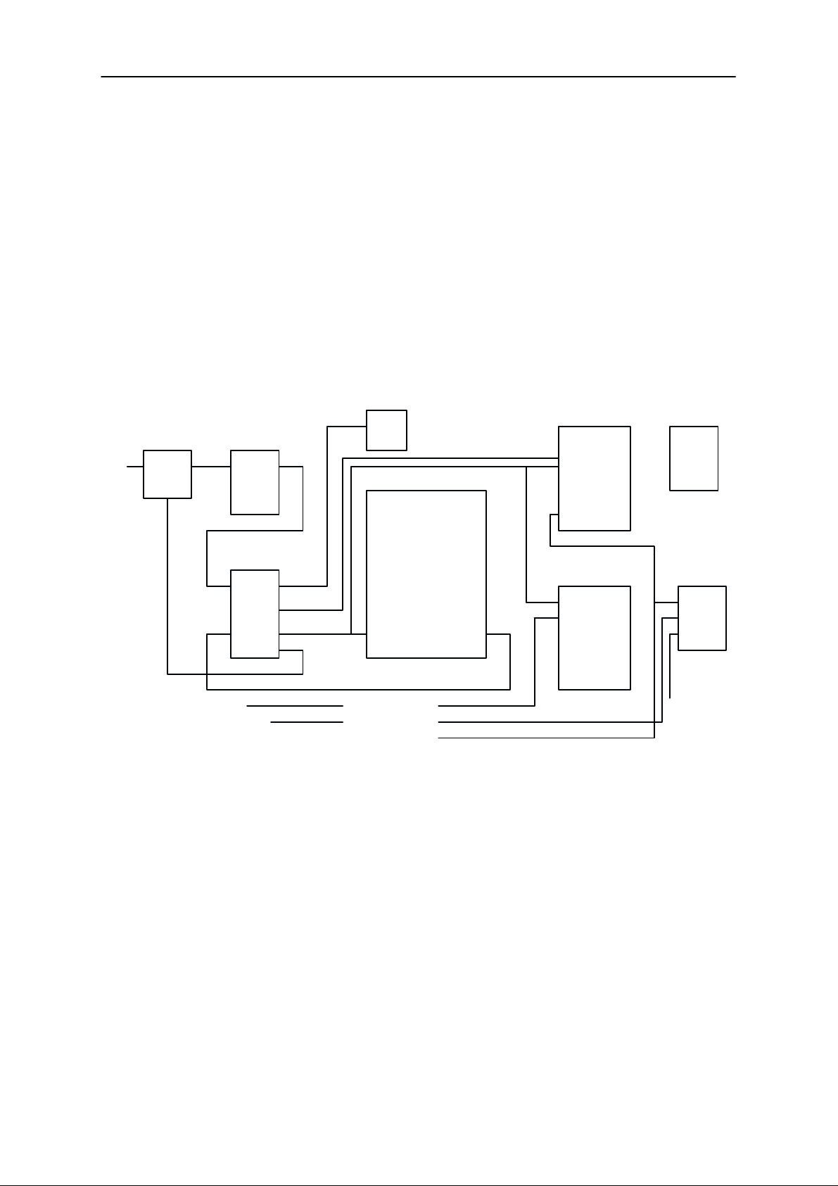
Power Distribution Diagram
UT4U Engine
PENTA
Charger
CCONT
Charge
control
VR8
VR9
VR10
VR11
VR12
VR1
VR2
VR3
VR4
VR5
VR6
VR7
VREF
VSIM
Technical Documentation
PA 1900 MHz
PA 800 MHz
RF
1900 MHz
800 MHz
Battery
VBB
V5V
UI Module
Baseband
COBBA
analog
Flash
ROM
Page 3 – 14
Original 11/99
Page 15
PAMS
NSC–3
Technical Documentation
External interfaces
4
Battery
Pack
3
Charger
IBI
Connector Name Notes
Antenna
US4U
ENGINE
6
Accessories
Bottom
connectorconnector
System Module US4U/US4RM/US4RSMD
User
28
22
Mic
Interface
Module
Display
Keyboard
Backlights
Speaker
Buzzer
Bottom connector + IBI connector Includes control, data, charging and audio sig-
nals
UI–connector includes keyboard, backlight, display,buzzer, call
led, and earpiece signals
Battery connector VBAT, GND, BTYPE, BTEMP
RF–interface Connection
Signals between baseband and User Interface section
The User interface section is implemented on separate UI board, which
connects to the engine board with a board to board spring connector.
User Interface module connection
The User interface section comprises the keyboard with keyboard lights,
display module with display lights, an earphone and a buzzer.
Earphone
The internal earphone is connected to the UI board by means of mounting springs for automatic assembly. The low impedance, dynamic type
earphone is connected to a differential output in the COBBA audio codec.
The voltage level at each output is given as reference to ground. Earphone levels are given to 32 ohm load.
Buzzer
Alerting tones and/or melodies as a signal of an incoming call are generated with a buzzer that is controlled with a PWM signal by the MAD. The
buzzer is a SMD device and is placed on the UI board.
Original 11/99
Page 3 – 15
Page 16
NSC–3
PAMS
System Module US4U/US4RM/US4RSMD
Baseband Module
Power Distribution
In normal operation the baseband is powered from the phone‘s battery.
The battery consists of one Lithium–cell. There is also a possibility to use
batteries consisting of three Nickel– cells. An external charger can be
used for recharging the battery and supplying power to the phone. The
charger can be either so called fast charger, which can deliver supply current up to 850 mA or a standard charger that can deliver around 300 mA.
VCXO
CHAPS
VCHAR
BATTERY
Technical Documentation
COBBA LCD–DRVR
MAD
VBAT
CCONT
PWM
V2V
VR1_SW
VR1
VR6
VBB
FLASH
SIO
VSIM
V5V
Vref
RF
VR1–VR7
Battery voltage VBAT is connected to CCONT which regulates all the supply voltages VBB, VR1–VR7, V2V, VR1_SW, VSIM and V5V. VR7 is divided into VR7 and VR7_bias. VR7_bias is for RF, because PA is heating
and this reduces the heat. CCONT enables automatically VR1, VBB,
V2V_core, VR6 and Vref in power–up.
VBB is used as baseband power supply for all digital parts, and it is
constantly on whenever the phone is powered up. There is also another
Baseband voltage, V2V, which is reserved for later version of MAD circuit.
V2V will be used as a lower core voltage for MAD internal parts, by supplying it to specific MAD core voltage pins. Until that time, VBB will be
used for all MAD pins. VSIM can be used as programming voltage for the
Flash memory, if re–flashing is needed after initial flash programming in
production. V5V is used for RF parts only.
VR1 is used for the VCXO supply. VR1_SW is derived from VR1 inside
CCONT, and is actually the same voltage, but can be separately switched
Page 3 – 16
Original 11/99
Page 17
PAMS
NSC–3
Technical Documentation
on and off. This VR1_SW is used as bias voltage for microphone, during
talk modes. Voltage VR6 is used in COBBA for analog parts and also
in RF parts. RFCEN signal to CCONT controls both the VR1 and VR6
regulators; they can be switched off in sleep modes, during standby.
CCONT regulators are controlled either through SIO from MAD or timing
sensitive regulators are controlled directly to their control pins. These two
control methods form a logical OR–function, i.e. the regulator is enabled
when either of the controls is active. Most of the regulators can be individually controlled.
CHAPS connects the charger voltage (VCHAR) to battery. MCU of MAD
controls the charging through CCONT. MAD sets the parameters to
PWM–generator in CCONT and PWM–output controls the charging voltage in charger.
When battery voltage is under 3.0V, CHAPS controls independently the
charging current to battery.
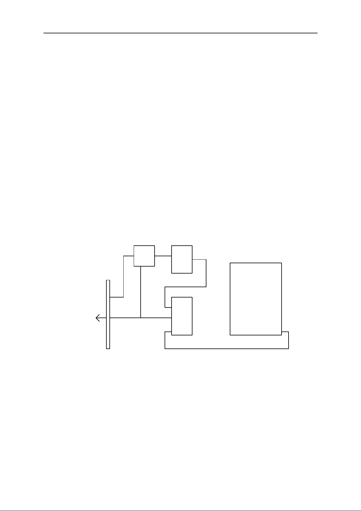
Charging Control
System Module US4U/US4RM/US4RSMD
System
Connector
To
charger
Charging is controlled by MCU SW, which writes control data to CCONT
via serial bus. CCONT output pin PWMOUT (Pulse Width Modulation)
can be used to control both the charger and the CHAPS circuit inside
phone.
2–wire charging
Vin
PWMOUT
Charging Control
CHAPS
BATTERY
MAD
CCONT
serial control
With 2–wire charging the charger provides constant output current, and
the charging is controlled by PWMOUT signal from CCONT to CHAPS.
PWMOUT signal frequency is selected to be 1 Hz, and the charging
switch in CHAPS is pulsed on and off at this frequency. The final charged
energy to battery is controlled by adjusting the PWMOUT signal pulse
width.
Original 11/99
Page 3 – 17
Page 18
NSC–3
PAMS
System Module US4U/US4RM/US4RSMD
Both the PWMOUT frequency selection and pulse width control are made
MCU which writes these values to CCONT.
3–wire charging
With 3–wire charging the charger provides adjustable output current, and
the charging is controlled by PWMOUT signal from CCONT to Charger,
with the bottom connector signal. PWMOUT signal frequency is selected
to be 32 Hz, and the charger output voltage is controlled by adjusting the
PWMOUT signal pulse width. The charger switch in CHAPS is constantly
on in this case.
Watchdog
VCXO
Technical Documentation
BATTERY
MAD COBBA
CCONT
32 kHz
VR1
VR6
VBB
SLCLK
MCU
LOGIC
SIO
Both MAD and CCONT include a watchdog, and both use the 32 kHz
sleep clock. The watchdog in MAD is the primary one, and this is called
SW–watchdog. MCU has to update it regularly. If it is not updated, logic
inside MAD gives reset to MAD. After the reset, MCU can read an internal status bit to see the reason for reset, whether it was from MAD or
CCONT. The SW–watchdog delay can be set between 0 and 63 seconds
at 250 millisecond steps; and after power–up the default value is the max.
time.
MAD must reset CCONT watchdog regularly. CCONT watchdog time can
be set through SIO between 0 and 63 seconds at 1 second steps. After
power–up the default value is 32 seconds. If watchdog elapses, CCONT
will cut off all supply voltages.
After total cut–off the phone can be re–started through any normal power–up procedure.
Page 3 – 18
Original 11/99
Page 19
PAMS
NSC–3
Technical Documentation
Power up
When the battery is connected to phone, nothing will happen until the
power–up procedure is initiated, for instance by pressing the power–button (or by connecting charger voltage). After that the 32kHz crystal oscillator of CCONT is started (can take up to 1 sec), as well as the regulators
are powered up.
If power down is done, and the battery remains connected, the 32 kHz
crystal oscillator keeps still running in the CCONT. When power–up is initiated again, the complete power–up sequence is like in the figure below.
This time the power–up sequence is faster, because the oscillator is already running.
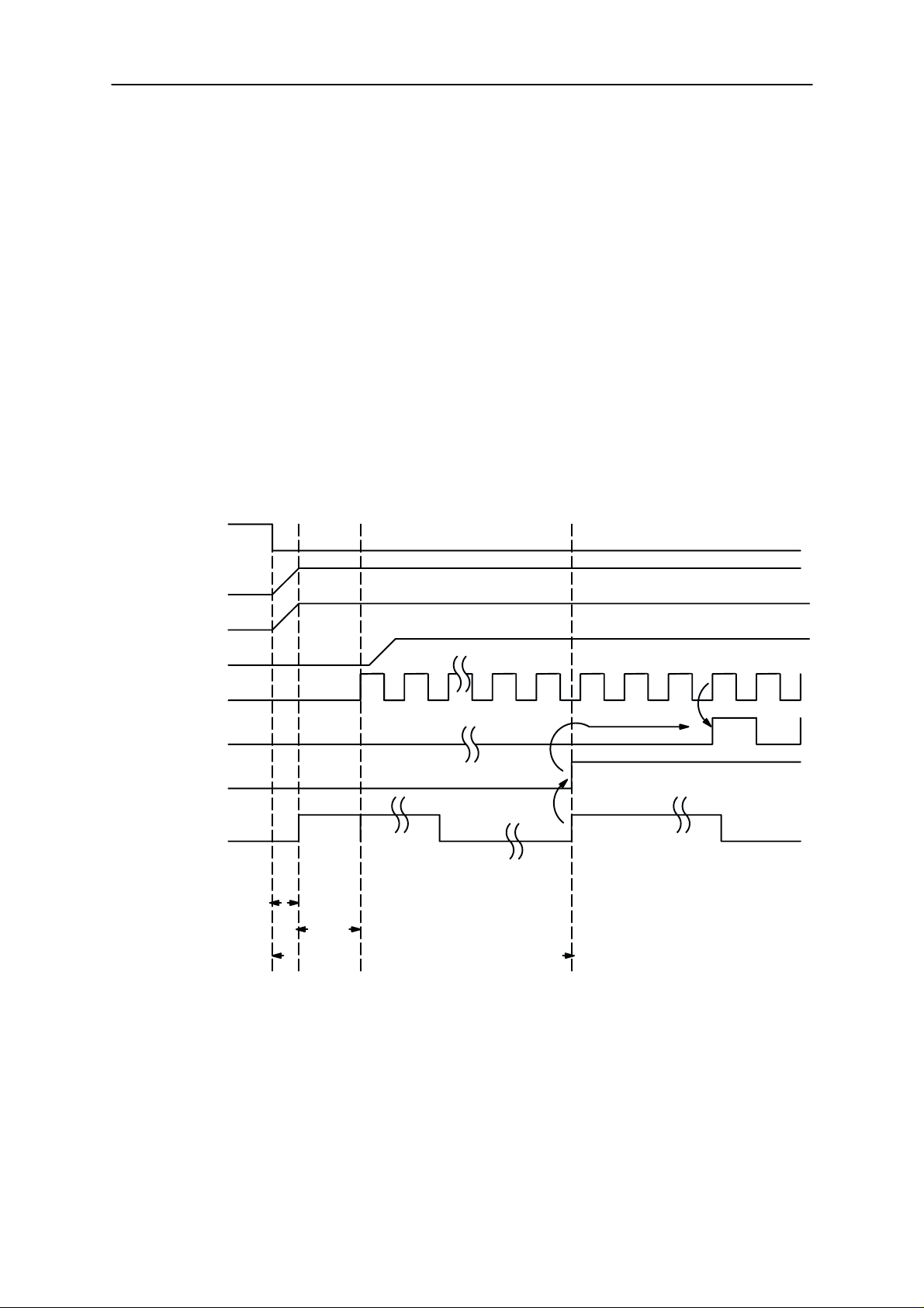
Power up when power–button is pushed
PWRONX
System Module US4U/US4RM/US4RSMD
VR1, VBB, VR6
RFCEN
RFCSETTLED
RFC (VCXO)
COBBACLK
PURX
SLCLK
t1
t2
t3
t1 < 1 ms
t2 1 – 6 ms, VCXO settled
t3 62 ms, PURX delay generated by CCONT
After PWR–key has been pushed, CCONT gives PURX reset to MAD and
COBBA, and turns on VR1, VBB and VR6 regulators (if battery voltage
has exceeded 3.0 V). VR1 supplies VCXO, VBB supplies MAD and digital
parts of COBBA, and VR6 supplies analog parts of COBBA and some RF
Original 11/99
Page 3 – 19
Page 20

NSC–3
PAMS
System Module US4U/US4RM/US4RSMD
parts. After the initial delay t2 VCXO starts to give proper RFC to COBBA
that further divides it to COBBACLK for MAD. COBBA will output the
COBBACLK only after the PURX reset has been removed. After delay t3
CCONT releases PURX and MAD can take control of the operation of the
phone.
After that MCU–SW in MAD detects that the PWR–key is still pushed and
shows the user that the phone is powering up by starting the LCD and
turning on the lights. MCU–SW must start also RF receiver parts at this
point.
CCONT will automatically power–up also VSIM–regulator (used for possible reFlashing), regardless of the control pin SIMPWR state, and the
regulator default voltage is 3V. VSIM voltage could be selected to be 5V,
by writing the selection via serial bus to CCONT, but that is not needed
with the new Flash versions (Jaguar).
V5V–regulator (for RF) default value is off in power–up, and can be controlled on via serial bus when needed.
Technical Documentation
IBI (Intelligent Battery Interface)
Phone can be powered up by external device (accessory or similar) by
providing a start pulse to the battery signal BTEMP; this is detected by
CCONT. After that the power–up procedure is similar to pushing power–
button.
Mixed trigger to power up
It is possible that PWR–key is pushed during charger initiated power–up
procedure or charger is connected during PWR–key initiated power up
procedure. In this kind of circumstances the power–up procedure (in HW
point of view) continues as nothing had happened.
When the Baseband HW is working normally and SW is running, SW detects that both conditions are fulfilled and then acts accordingly.
Power Off
Power off by pushing Power–key
MAD (MCU SW) detects that PWR–key is pressed long enough time. After that the lights and LCD are turned off. MCU stops all the activities it
was doing (e.g. ends a call), sends power off command to CCONT (i.e.
gives a short watchdog time) and goes to idle–task. After the delay
CCONT cuts all the supply voltages from the phone. Only the 32 kHz
sleep clock remains running.
Note that the phone doesn’t go to power off (from HW point of view) when
the charger is connected and PWR–key is pushed. It is shown to user
that the phone is in power off, but in fact the phone is just acting being
powered off (this state is usually called acting dead).
Page 3 – 20
Original 11/99
Page 21

PAMS
NSC–3
Technical Documentation
Power off when battery voltage low
During normal discharge the phone indicates the user that the battery will
drain after some time. If not recharged, SW detects that battery voltage is
too low and shuts the phone off through a normal power down procedure.
Anyway, if the SW fails to power down the phone, CCONT will make a reset and power down the phone if the battery voltage drops below 2.8 V.
Power off when fault in the transmitter
If the MAD receives fault indication, from the line TXF, that the transmitter
is on although it shouldn’t be, the control SW will power down the phone.
Sleep Mode
The phone can enter SLEEP only when both MCU and DSP request it. A
substantial amount of current is saved in SLEEP. When going to SLEEP
following things will happen
System Module US4U/US4RM/US4RSMD
1. Both MCU and DSP enable sleep mode, set the sleep timer
and enter sleep mode
2. RFCEN and RFCSETTLED –> 0 –> COBBACLK will stop
(gated in COBBA). Also VR1 is disabled –> VCXO supply voltage is cut off –> RFC stops.
3. LCD display remains the same, no changes
4. Sleep clock (SLCLK) and watchdog in CCONT running
5. Sleep counter in MAD running, uses SLCLK
Waking up from the Sleep–mode
In the typical case phone leaves the SLEEP–mode when the SLEEP–
counter in MAD expires. After that MAD enables VR1 ⇒ VCXO starts running ⇒ after a pre–programmed delay RFCSETTLED rises => MAD receives COBBACLK clock ⇒ MAD operation re–starts.
There are also many other cases when the SLEEP mode can be interrupted, in these cases MAD enables the VR1 and operation is started
similarly
– some MCU or DSP timer expires
– DSP regular event interrupt happens
– MBUS activity is detected
– FBUS activity is detected
– Charger is connected, Charger interrupt to MAD
– any key on keyboard is pressed, interrupt to MAD
– HEADSETINT, from system connector XMIC line (EAD)
– HOOKINT, from system connector XEAR line
Original 11/99
Page 3 – 21
Page 22

NSC–3
PAMS
System Module US4U/US4RM/US4RSMD
Baseband submodules
CTRLU
CTRLU comprises MAD ASIC (MCU, DSP, System Logic) and Memories.
The environment consists of three memory circuits (FLASH,SRAM,EE-
PROM), 22–bit address bus and 8/16–bit data bus. Besides there are
ROM1SELX, ROM2SELX, RAMSELX and EEPROMSELX signals for chip
select.
MCU main features
System control
Cellular Software (CS)
Cellular Software takes care of communication with switching
office, as well call build–up, maintenance and termination.
Technical Documentation
Communication control
M2BUS is used to communicate to external devices. This interface is also used for factory testing, service and maintenance purposes.
User Interface (UI)
PWR–key, keyboard, LCD, flip/door switch, backlight, mic, ear
and alert (buzzer, vibra, led) control. Serial interface from MAD
to LCD (common for CCONT).
Authentication
Authentication is used to prevent fraud usage of cellular
phones.
RF monitoring
RF temperature monitoring by VCXOTEMP, ADC in CCONT.
Received signal strength monitoring by RSSI, ADC in CCONT.
False transmission detection by TXF signal, digital IO–pin.
Power up/down and Watchdog control
When power key is pressed, initial reset (PURX) has happened
and default regulators have powered up in CCONT, MCU and
DSP take care of the rest of power up procedures (LCD, COBBA, RF). MCU must regularly reset Watchdog counter in
CCONT, otherwise the power will be switched off.
Accessory monitoring
Page 3 – 22
Accessory detection by EAD (XMIC/HEADSETINT), AD–con-
verter in CCONT. Connection (FBUS) for data transfer.
Original 11/99
Page 23

PAMS
NSC–3
Technical Documentation
Battery and charging monitoring
MCU reads the battery type (BTYPE), temperature (BTEMP)
and voltage (VBAT) values by AD–converter in CCONT, and
phone’s operation is allowed only if the values are reasonable.
Charging current is controlled by writing suitable values to
PWM control in CCONT. MCU reads also charger voltage
(VCHAR) and charging current values (ICHAR).
Production/after sales tests and tuning
Flash and EEPROM loading, baseband tests, RF tuning
Control of CCONT via serial bus
MCU writes controls (regulators on/off, Watchdog reset,
charge PWM control) and reads AD–conversion values. For
AD–conversions MCU gives the clock for CCONT (bus clock),
because the only clock in CCONT is sleep clock, which has too
low frequency.
System Module US4U/US4RM/US4RSMD
DSP main features
DSP (Digital Signal Processor) is in charge of the channel and speech
coding according to the IS–136 specification. The block consists of a DSP
and internal ROM and RAM memory. The input clock is 9.72 MHz, and
DSP has it’s own internal PLL–multiplier. Main interfaces are to MCU,
and via System Logic to COBBA and RF.
System Logic main features
– MCU related clocking, timing and interrupts (CTIM)
– DSP related clocking, timing and interrupts (CTID)
– DSP general IO–port
–reset and interrupts to MCU and DSP
– interface between MCU and DSP (API)
– MCU interface to System Logic (MCUif)
– MCU controlled PWMs, general IO–port and USART for MBUS (PUP)
– Receive Modem (Rxmodem)
– Interface to Keyboard, CCONT and LCD Drivers (UIF)
– Interface to MCU memories, address lines and chip select decoding
(BUSC)
– DSP interface to System Logic (DSPif)
– serial accessory interface (AccIf, DSP–UART)
– Modulation, transmit filter and serial interface to COBBA (MFI)
– Serial interface for RF synthesizer control (SCU)
Memories
The speed requirement of FLASH and SRAM is assumed to be 120 ns.
Original 11/99
Page 3 – 23
Page 24

NSC–3
PAMS
System Module US4U/US4RM/US4RSMD
FLASH
– size 8 Mbit (512k * 16 bit), optional 4 Mbit and 16 Mbit, all made layout
compatible by having additional higher address lines ready in the layout.
Flash memory contains the main program code for the MCU, and EEPROM default values.
SRAM
– size 64k * 8 bit (US4U Phase1) / 128k/256 * 8 bit (US4RM Phase2)
both in STSOP32 package
EEPROM
– size 16k * 8 bit, optional 8k * 8 bit
– serial or optional parallel interface can be used (MAD1 supports both),
but serial interface is used.
AUDIO–RF
Audio interface and baseband–RF interface converters are integrated into
COBBA circuit.
Technical Documentation
Cobba main features
The codec includes microphone and earpiece amplifier and all the necessary switches for routing. There are 2 different possibilities for routing;
internal and external devices. There are also all the AD– and DA– converters for the RF interface.
New solution, DEMO block, is used for FM–demodulation in analog
mode.
A slow speed DA–converter provides automatic frequency control (AFC).
In addition, there is a DA–converters for transmitter power control (TXC).
COBBA also passes the RFC (19.44 MHz) to MAD as COBBACLK (9.72
MHz).
COBBA is connected to MAD via two serial busses:
– RXTXSIO, for interfacing the RF–DACs and DEMO; and also for audio
codec and general control. Signals used: COBBACLK (9.72 MHz, from
COBBA), COBBACSX, COBBASD (bi–directional data) and COBBADAX (data ready flag for rx–samples).
– Codec SIO, for interfacing the audio ADCs / DACs (PCM–samples).
Signals: PCMDCLK (data clock 1.08 MHz / 1.215 MHz), PCMSCLK
(frame sync 8.0 kHz / 8.1 kHz), PCMTxdata and PCMRxdata.
Page 3 – 24
Original 11/99
Page 25

PAMS
NSC–3
Technical Documentation
Speech processing
The speech coding functions are performed by the DSP in the MAD and
the coded speech blocks are transferred to the COBBA for digital to analog conversion, down link direction. In the up link direction the PCM coded
speech blocks are read from the COBBA by the DSP.
There are two separate interfaces between MAD and COBBA: 2 serial
buses. The first serial interface is used to transfer all the COBBA control
information (both the RFI part and the audio part). The second serial interface between MAD and COBBa includes transmit and receive data,
clock and frame synchronisation signals. It is used to transfer the PCM
samples. The frame synchronisation frequency is 8 kHz ( the sample rate
is in digital mode 8.0 kHz and in analog mode 8.1 kHz) which indicates
the rate of the PCM samples and the clock frequency is 1 MHz. COBBA is
generating both clocks.
Alert Signal Generation
System Module US4U/US4RM/US4RSMD
A buzzer is used for giving alerting tones and/or melodies as a signal of
an incoming call. The buzzer is controlled with a BuzzerPWM output signal from the MAD. A dynamic type of buzzer must be used since the supply voltage available can not produce the required sound pressure for a
piezo type buzzer. The low impedance buzzer is connected to an output
transistor that gets drive current from the PWM output. The alert volume
can be adjusted either by changing the pulse width causing the level to
change or by changing the frequency to utilize the resonance frequency
range of the buzzer.
A vibra alerting device is used for giving silent signal to the user of an incoming call. The device is controlled with a VibraPWM output signal from
the MAD. The vibra alert can be adjusted either by changing the pulse
width or by changing the pulse frequency. The vibra device is not inside
the phone, but in a special vibra battery.
Original 11/99
Page 3 – 25
Page 26

NSC–3
PAMS
System Module US4U/US4RM/US4RSMD
PWRU
PWRU comprises CCONT circuit and CHAPS circuit.
CCONT main features
CCONT generates regulated supply voltages for baseband and RF.
There are seven 2.8 V linear regulators for RF, one 2.8 V regulator for
baseband, one special switched output (VR1_SW), one programmable
2V output (V2V), one 3/5 V output (VSIM), one 5V output (V5V), and one
1.5 V +/– 1.5% reference voltage for RF and COBBA.
Other functions are
– power up/down procedures and reset logic
– charging control (PWM), charger detection
– watchdog
– sleep clock (32 kHz) and control
– 8–channel AD–converter.
Technical Documentation
CHAPS main features
CHAPS comprises the hardware for charging the battery and protecting
the phone from over–voltage in charger connector.
The main function are
– transient, over–voltage and reverse charger voltage protection
– limited start–up charge current for a totally empty battery
– voltage limit when battery removed
– with SW protection protection against too high charging current
Page 3 – 26
Original 11/99
Page 27

PAMS
NSC–3
Technical Documentation
RF Module
RF Frequency Plan
Intermediate frequencies of the RX are the same in all operation modes.
LO and modulator frequencies in TDMA800 operation modes. See figure
1 for details.
869.01–893.97 MHz
1st IF
116.19 MHz
System Module US4U/US4RM/US4RSMD
2nd IF
450 kHz
116.64 MHz
IF2 A–mode
450 kHz
IF2 D–mode
450 kHz
LO 1
LO 3 PLL
824.01–848.97 MHz
985.20–1010.16 MHz
161.19 MHz
322.38 MHz
LO 2
DC Characteristics
Power Distribution Diagram
Power distribution in a 800 MHz DAMPS phone. Current consumptions in
the diagrams are only suggestive.
PLL
f
f/2
PLL
VCTCXO
19.44 MHz
2f
f
PLUSSA
f
3f
58.32 MHz
19.44 MHzRFC
Original 11/99
Page 3 – 27
Page 28

NSC–3
PAMS
System Module US4U/US4RM/US4RSMD
DAMPS OPERATION
2 mA
RFCEN
SPWR1
TXPWR1
RXPWR
SPWR2
(via serial bus)
TXPWR3
TXP
VR1
VREF
VR2
V5V
VR6
VR5
VR4
VR3
CCONT
VR7
3 mA
8 mA
RX FRONT
END
19 mA
3 * Multiplier
30 mA
4 mA
3 mA
15 mA
Enable
3 mA
VCTCXO19.44 MHz
& Buffer
UHF–
VCO
2 mA
1 mA
TQ UHF
LO–buffer
COBBA_D
(Analog)
Detector
IF1 –
amp.
VHF
VCO
TX
mixer
TX PA
MMIC bias
Technical Documentation
2 mA
6 mA
8 mA
5 mA (peak)
2 mA
1 mA
35 mA
26 mA/5.6 mA
1 mA
Freq.
doubler
VHF
presc.
Bias
UHF
presc.
& PLL
Phase
det.
Digital
supply
Power
control
Modulator
Digital m.
IF– parts
Analog m.
IF– parts
Limiter
PLUSSA
Control
block
MODE
VBATT
Page 3 – 28
VRBB
55 mA
TX
driver
BASEBAND
TX PA
SDATA
SCLK
SENA1
Original 11/99
Page 29

PAMS
NSC–3
Technical Documentation
System Module US4U/US4RM/US4RSMD
Power Distribution – Typical Currents
800 MHz
Ext.
Standby
[mA]
VR1 3.0 / 0.0 3.0 9.0 3.0 / 0.0 9.0
VR2 16.0 / 0.0 16.0 16.0 16.0 / 0.0 16.0
VR3 0.0 0.0 23.0 0.0 13.0
VR4 11.6 / 0.0 11.6 11.6 32 / 0.0 12.8*
VR5 0.0 0.0 37.0 0.0 13.0 **
VR6 2.0 / 0.1 2.0 32.0 *** 2.0 / 0.1 32.0 ***
VR7 0.0 0.0 58.0 0.0 19.2 ’
VR8 19.0 / 0.0 19.0 19.0 19.0 / 0.0 7.6 ’’
VR9 0.0 0.0 0.0 0.0 0.0
800 MHz
Analog
Control
Channel
[mA]
800 MHz
Analog
Traffic
Channel
[mA]
800 MHz
Digital
Control
Channel
[mA]
800 MHz
Digital
Traffic
Channel
[mA]
VR10 0.0 0.0 0.0 0.0 0.0
VR11 0.0 0.0 0.0 0.0 0.0
VR12 0.0 0.0 0.0 0.0 0.0
V5V 5.0 / 0.0 5.0 5.0 5.0 / 0.0 5.0
Total 56.6 / 0.1 56.6 210.6 77.0 / 0.1 127.6
NOTES: * Mean value (ON/OFF=8/20ms), peak current 32.0 mA
** Mean value (ON/OFF=7/20ms), peak current 37.0 mA
*** Cobba_D mean current consumption estimated to be 30 mA
’ Mean value (ON/OFF=6.6/20ms), peak current 180.0 mA
’’ Mean value (ON/OFF=8/20ms), peak current 10.0 mA
Original 11/99
Page 3 – 29
Page 30

NSC–3
PAMS
System Module US4U/US4RM/US4RSMD
Functional Description
Receiver
DAMPS800 RX
The receiver is a double conversion receiver. Most of the RX functions
are integrated in two ICs, namely receiver front end and PLUSSA. Receiver front end contains a LNA and the 1st mixer. Analog and digital IF–
parts are integrated in the PLUSSA.
The received RF signal from the antenna is fed via a duplex filter to the
receiver unit. The signal is amplified by a low noise preamplifier. In digital mode the gain of the amplifier is controlled by the AGC2 control line.
The nominal gain of 17 – 19 dB is reduced in the strong signal condition
about 15 dB (in the digital mode). After the preamplifier the signal is filtered by SAW RF filter. The filter rejects spurious signals coming from the
antenna and spurious emissions coming from the mixer and IF parts.
AGC2 gain step is also used to improve receiver’s performance against
spurious responses in real field situations, when received signal level is
high enough for reduced gain and there are radio signals causing on
channel intermodulation results.
Technical Documentation
The filtered RF–signal is down converted by an active mixer. The frequency of the first IF is 116.19 MHz. The first local signal is generated in
the UHF synthesizer. The IF signal is fed to a SAW IF–filter. The filter re-
jects intermodulating signals and the second IF image signal. The filtered
1st IF is amplified and fed to the receiver section of the integrated RF circuit PLUSSA, which has separate IF paths for analog and digital modes
of operation.
In digital mode the IF1 signal is amplified by an AGC amplifier, which has
gain control range of 57 dB. The gain is controlled by an analog signal via
AGC1–line. The amplified IF signal is down converted to the second IF in
the mixer of PLUSSA. The second local signal is the 6th overtone of the
19.44 MHz VCTCXO. LO frequency multiplier is implemented in two
stages. First multiplication by 3 is done within the VCTCXO–module and
the second multiplication by 2 is done in the PLUSSA.
The second IF frequency is 450 kHz. The second IF is filtered by a ceramic filter. The filter rejects signals of the adjacent channels. The filtered second IF is fed back to PLUSSA, where it is amplified and fed out
to COBBA_D via balanced IF2D lines.
In analog mode the filtered and amplified IF1 signal is fed to a mixer. This
mixer has been optimized for low current consumption. After this the mixer down converted signal is fed through the same IF2 filter as in digital
mode and finally it is amplified in the limiter amplifier. The limited IF2 signal is fed via balanced IF2A lines to COBBA_D, which has a FM–detector.
The limiter amplifier produces also a RSSI voltage for analog mode field
strength indication.
Page 3 – 30
Original 11/99
Page 31

PAMS
NSC–3
Technical Documentation
Transmitter
DAMPS800 TX
The TX intermediate frequency is modulated in digital mode by an I/Q
modulator contained in the transmitter section of PLUSSA IC. The TX I
and TXQ signals are generated in the COBBA_D interface circuit and
they are fed differentially to the modulator. In analog mode the FM modulation is also generated in the I/Q modulator.
Intermediate frequency level at the modulator output is controlled via serial bus. Modulator output level control is used to tune out tolerances of the
TX chain and expand the range of the VGA. The output level of the modulator is typically –18dBm on the highest power level (PL2). For lower power levels modulator output is reduced by 4 dB for each power level. In
analog mode PLUSSA modulator has fixed output level. All power levels
are defined by adjusting driver amplifier’s gain.
The output signal from PLUSSA modulator is filtered to reduce harmonics
and RX–band noise. The final TX signal is achieved by mixing the UHF
VCO signal and the modulated TX intermediate signal in an active mixer.
After the mixing TX signal is amplified by a driver stage. Driver amplifier
has a gain control stage, which is used for power level adjustment and
generating ramps. From driver stage the signal is fed trough TX filter to
PA MMIC.
System Module US4U/US4RM/US4RSMD
The PA amplifies the signal TX 27–30 dB. Amplified TX signal is filtered in
duplex filter. Then signal is fed to the antenna switch, where the signal is
coupled either to antenna or to external antenna connector. The typical
maximum output level is 600 mW.
The power control loop controls the gain of the driver amplifier. The power detector consists of a directional coupler and a diode rectifier. The output voltage of the detector is compared to TXC voltage in PLUSSA. The
power control signal (TXC), comes from the RF interface circuit, COBBA_D. TXP signal sets driver power down to ensure off–burst level requiremensts.
False transmission indication is used to protect transmitter against false
transmission caused by component failure. Protection circuit is in Plussa.
The level for TXF is set by internal resistor values in Plussa.
Frequency Synthesizers
The stable frequency reference for the synthesizers and base band circuits is a voltage controlled temperature compensated crystal oscillator
VCTCXO. Frequency of the oscillator is 19.44 MHz. It is controlled by an
AFC voltage, which is generated in the base band circuits. In digital mode
operation, the receiver is locked to base station frequency by AFC. Next
to detector diode, there is a sensor for temperature measurement. Voltage RFTEMP from this sensor is fed to baseband for A/D conversion.
Original 11/99
Page 3 – 31
Page 32

NSC–3
PAMS
System Module US4U/US4RM/US4RSMD
This information of RF PA–block temperature is used as input for compensation algorithms.
The ON/OFF switching of the VCTCXO is controlled by the sleep clock in
the baseband via RFCEN. Other parts of the synthesizer section are 1
GHz VCO, 2 GHz VCO, VHF VCO, PLL for 2 GHz VCO and PLL sections
of the Plussa IC.
DAMPS800 operation
1GHz UHF synthesizer generates the down conversion injection for the
receiver and the up conversion injection for the transmitter. UHF frequency is 985.20 ... 1010.16 MHz, depending on the channel which is used.
1GHz UHF VCO is a module. The PLL circuit is dual PLL, common for
both UHF and VHF synthesizers. These PLLs are included in the PLUSSA IC.
LO signal for the 2nd RX mixer is multiplied from the VCTCXO frequency
as described above.
Technical Documentation
VHF synthesizer is running only on digital or analog traffic channel.
322.38 MHz signal (divided by 2 in Plussa) is used as a LO signal in the
I/Q modulator of the transmitter chain.
Supply voltages in different modes of operation
800
MHz
Ext.
Stadby
VR1 ON/OFF ON ON ON/OFF ON
VR2 ON/OFF ON ON ON/OFF ON
VR3 OFF OFF ON OFF ON
VR4 ON/OFF ON ON ON/OFF ON/OFF
VR5 OFF OFF ON OFF ON/OFF
VR6 ON ON/OFF ON ON/OFF ON
VR7 OFF OFF ON OFF ON/OFF
VR8 ON/OFF ON ON ON/OFF ON/OFF
800
MHz
Analog
Control
Channel
800
MHz
Analog
Traffic
Channel
800
MHz
Digital
Control
Channel
800
MHz
Digital
Traffic
Channel
Page 3 – 32
VR9 OFF OFF OFF OFF OFF
VR10 OFF OFF OFF ON/OFF* ON/OFF*
VR11 OFF OFF OFF OFF OFF
VR12 OFF OFF OFF OFF OFF
VSIM ON/OFF ON ON ON/OFF ON
NOTE: * ON during interband MAHO
Original 11/99
Page 33

PAMS
NSC–3
Technical Documentation
Software Compensations
Power Levels (TXC) vs. Temperature
Because of wide temperature range and poor cooling of the RF block, it is
neccessary to compensate the effect of temperature on the output power.
To monitor this environment change, temperature measurement is done
by using NTC resistor. Factor table is used for temperature compensation,. The table contains common values for all power levels and operating modes. Table values are defined without factory measurements. Temperature is measured and right compensation value is added to TXC–val-
ue. Requirement for compensation update is for every 1 minutes or after
every 5 degrees C of temperature change. This means, that during analog mode transmission there will be a need for temperature reading and
TXC compensation update. Because of poor cooling of RF block and insufficient linearity in high temperatures, output power is reduced from level 2 to level 2.5 when temperature inside the phone is above +55 C in
analog mode and above +60 C in digital mode.
System Module US4U/US4RM/US4RSMD
Power Levels (TXC) vs. Channel
Duplexer frequency response ripple is compensated by software. Power
levels are calibrated on four channels in production. Values for channels
between these tuned channels are calculated by using linear interpolation.
Power levels vs. Battery Voltage
For saving battery capacity and because of insufficient linearity in digital
mode, output power is decreased from level 2 to level 2.5, when battery
voltage drops below 3.3V. (tbd.). The power reduction is done linearly as
a function of battery voltage. Vcc 3.3V ... 3.1V –> PL2 ... PL2.5.
TX Power Up/Down Ramps
Transmitter output power up/down ramps are controlled by SW. A special
ramp tables are used for that. Requirement is for nine different ramps in
digital mode for both operating bands and one ramp for analog mode.
Separate ramps are used in power up and power down ramps.
Modulator Output Level
For optimum linerity and efficiency the output level of the modulator is adjusted in the production. AGC amplifier is used as 2 dB step attenuator to
define power levels. The 0 dB level is the production tuned reference level.
Digital Mode RSSI
Digital mode RSSI vs. input signal is calibrated in production, but RSSI
vs. temperature and RSSI vs. channel are compensated by software.
Original 11/99
Page 3 – 33
Page 34

NSC–3
PAMS
System Module US4U/US4RM/US4RSMD
RF Block Specifications
Receiver
DAMPS 800 Mhz Front End
Parameter Minimum Typical /
Gain, LNA gain enabled
(gain variations vs temp. included)
Gain, LNA gain disabled –10 dB
Gain step 15 dB
Gain variation vs temp –30...+85 dC,
amplifier enabled, ref. to nominal gain
Noise figure, LNA enabled 2.5 3.0 dB
Technical Documentation
Maximum Unit /
Nominal
19 21 23 dB
1.5 dB
Notes
First IF Filter
Parameter Minimum Typical /
Nominal
Operation frequency 116.19 MHz
Supply voltage 2.7 2.8 2.9 V
Current consumption 1.0 1.5 mA
Insertion gain 10 14 dB
Noise figure 3 dB
IIP3 –20 dBm
Input impedance TBD matched to the IF filter
Output impedance TBD matched to PLUSSA
Maximum Unit / Notes
Page 3 – 34
Original 11/99
Page 35

PAMS
NSC–3
Technical Documentation
System Module US4U/US4RM/US4RSMD
Transmitter
RF Characteristics
Item DAMPS
TX frequency range 824.01...848.97 MHz
Type Upconversion
Intermediate frequency 161.19 MHz
Nominal power on highest power level 0.6 W ( 27.8 dBm)
Power control range 30+38 dB
Maximum rms error vector 12.5 %
Power Levels
( see tuning table within Section: tuning Instructions (pages 17 & 18).
Synthesizers
UHF
Parameter UHF 800MHz
analog mode
rx/tx injec-
tion
Frequency range 985.20 ...
1010.16
Reference frequency 30 30 kHz
Reference peaks @ 30 kHz
@ 60 kHz
2 x fo level –20 –20 dBc
Phase noise, fo 60 kHz
fo 120 kHz
Phase error – 4
Residual FM
Filters: 300 Hz HP
3 kHz LP
–31
–70
–115
150 – Hz, max
UHF 800MHz
digital mode
rx/tx slot
985.20 ...
1010.16
–38
–57
–101
–121
Unit /
Notes
MHz
dBc, max
dBc/Hz,
max
d
, max
rms
Frequency settling time
within 3 kHz
within 30 Hz
Start up settling time 30 3 ms, max
20
1.4
2.0
ms, max
Original 11/99
Page 3 – 35
Page 36

NSC–3
PAMS
System Module US4U/US4RM/US4RSMD
VHF
Parameter VHF, 800MHz
analog mode
tx injection
Frequency range 322.38 322.38 MHz
Reference frequency 30 30 kHz
Reference peaks @ 30 kHz
@ 60 kHz
2 x fo level –30 –30 dBc
Phase noise, fo 60 kHz
fo 120 kHz
Phase error 2 2
Frequency settling time
within 3 kHz
within 30 Hz
Start up settling time 20 20 ms, max
–31
–66
–105 –105 dBc/Hz,
20 20
VHF, 800MHz
digital mode
rx/tx slot
–41
–60
Unit /
Notes
dBc, max
max
d
, max
rms
ms, max
Technical Documentation
Output Levels
Parameter Minimum Typical /
2G UHF synthesizer to Lo buffer
level
resistive load
parallel capacitance
1G UHF synthesizer to TX mixer
level
impedance
VHF synthesizer to PLUSSA
level
resistive load
parallel capacitance
VCTCXO 19.44 MHz to BB
level
resistive load
parallel capacitance
VCTCXO 19.44 MHz to PLUSSA
level
resistive load
parallel capacitance
100
1k
1000
10k
100
Nominal
tbd
tbd
tbd
tbd
tbd
tbd
Maximum Unit /
Notes
–10
–5 dBm
10
dBm
W
pF
W
mV
W
pF
mV
W
pF
mV
W
pF
pp
pp
pp
VCTCXO 58.32 MHz to PLUSSA
3 * fo level
fo and 2xfo level
harmonic supression
resistive load
parallel capacitance
Page 3 – 36
50
–25
–25
5k
tbd
100 mV
dBc
dBc
W
pF
pp
Original 11/99
Page 37

PAMS
regul.,
tors in dual band
RXPWR1
IF1–amp
NSC–3
Technical Documentation
Connections
RF–Baseband signals
Signal
name
VBAT battery RF
VREF CCONT Plussa
VR1 CCONT Plussa,
From/
Control
/
RFCEN
To Parameter Min Typ Max Unit Function
2V8
regul.,
PA
VCTCXO,
2GHz
PLL
System Module US4U/US4RM/US4RSMD
Voltage 3.1 3.6 5.3 V
Voltage during TX 3.0 3.6 5.0 V
Current 1200 mA
Voltage 1.478 1.50 1.523 V
Current 10 uA
Voltage 2.7 2.8 2.85 V
Current, tdma 800 3.0 7 9 mA
Current, tdma1900 3.0 17 19 mA
Supply voltage for
discrete 2V8 regulators in dual band
phone and PA
PLUSSA reference
voltage
Supply for VCTCXO &
multiplier, Plussa VHF
prescaler and bias and
2 GHz PLL
VR2 CCONT Plussa,
/
SPWR1
VR3 CCONT VHF–
/
SPWR2
(via serial
bus)
VR4 CCONT Plussa,
/
RXPWR1 IF1–amp
VR5 CCONT Plussa,
/
TXPWR1
VR6 CCONT Plussa
VR7 CCONT TX PA
TXP1
UHF
VCO1
VCO,
LO–buff,
TX mixer
VCTCXO
TX pwr
control
disc.PLL
Cobba_D
Voltage 2.7 2.8 2.85 V
Current, tdma800 14 16 20 mA
Current, tdma1900 off mA
Voltage 2.7 2.8 2.85 V
Current, tdma800 20 24 30 mA
Current, tdma1900 4 9 12 mA
Voltage 2.7 2.8 2.85 V
Current, anal.RX 10 12 15 mA
Current, digi.RX 30 32 34 mA
Voltage 2.7 2.8 2.85 V
Current, TX–mode 33 37 41 mA
Voltage 2.7 2.8 2.85 V
Current (RF block) 2.0 3.0 mA
Voltage 2.7 2.8 2.85 V
Current, tdma800 55 60 mA
Supply voltage for
tdma 800 UHF VCO
and prescaler
Supply for VHF VCO,
LO buffer, tdma800 TX
mixer and TXF
Supply for Plussa IF–
parts, IF1–amp.
Supply for Plussa
modulator, TX pwr
control
Plussa & disc PLL:
digital supply ,
Cobba_D:
analog supply
TX PA and driver supply
VR7_bias CCONT TX PA
TXP1 &
MODE
V5V CCONT PLUSSA
/
RFCEN
RFTEMP RF CCONT Voltage 0 1.5 V RF temperature sen-
Original 11/99
Voltage 2.7 2.8 2.85 V
Current, tdma800 3 mA
Voltage 4.8 5.0 5.2 V
Current 3.0 5.0 mA
TX PA bias
800 band
Plussa and discrete
synthesizer phase det
sor (47 k NTC to GND)
Page 3 – 37
Page 38

NSC–3
mode PA
W
PGA = 0 dB
PAMS
System Module US4U/US4RM/US4RSMD
Signal
name
AFC Cobba_D VCTCXO
AGC1 Cobba_D PLUSSA
Control
Voltage Min 0.05 1.2 2.25 V
Resolution 11 bits
Load resistance 10 kW
(dynamic)
Load resistance
(DC)
Voltage Min 0.5 1.40 V
Load resistance 10 kW
Load capacitance 10 pF
Resolution 10 bits
Timing inaccuracy 8 us
Technical Documentation
Automatic frequency
control signal for
VCTCXO. When DAC
VCTCXO. When DAC
is switched OFF AFC
output is in high–Z
110 kW
mode
Digital mode receiver
gain control.
DSP
FunctionUnitMaxTypMinParameterToFrom/
AGC2 MAD RX LNA
(CTID
AGC2,
AGC2,
genpio)
BAND Cobba_D VHF
VCO
1)
1)
MODE MAD Analog/
digital
mode PA
bias con-
trol
Logic high ”1” 2.0 V
Logic low ”0” 0.7 V
Sink/source curr. 20 uA
Load capacitance 10 pF
Timing inaccuracy 8 us
Logic high ”1” 2.1 V TDMA1900 operation
Logic low ”0” 0 0.4 V TDMA800 operation
Sink/source curr. 1.0 mA
Load capacitance 10 pF
Timing inaccuracy 1 ms
Logic high ”1” 2.1 V Digital 800 operation
Logic low ”0” 0 0.4 V Analog 800 operation
Sink/source curr. 2.0 mA
Load capacitance tbd pF
Timing inaccuracy ms
LNA gain switch.
Polarity: 0=reduced
1=normal
DSP
DSP, MCU
DSP
IF2AP/ PLUSSA Cobba_D
IF2AN
IF2DP/ PLUSSA Cobba_D
IF2DN
Page 3 – 38
IF2 frequency 450 kHz
Output level, 0.6 Vpp
Load resistance 10 k
Load capacitance 5 pF
IF2 frequency 450 kHz
Output level 170 1400 mVpp
Source imp. 600 W
Original 11/99
Differential IF2–signal
from limiter to DEMO
detector in Cobba_D
detector in Cobba_D
Differential IF2–signal
to RX A/D–converter,
PGA = 0 dB
Page 39

PAMS
SCLK)
PLL
NSC–3
Technical Documentation
Signal
name
RFC VCTCXO Cobba_D
RFCEN MAD
RSSI PLUSSA CCONT
Control
(CTID,
(CTID,
RFCEN)
CCONT,
Cobba_D
System Module US4U/US4RM/US4RSMD
FunctionUnitMaxTypMinParameterToFrom/
Frequency 19.44 MHz
Signal amplitude 0.2 1.0 Vpp
Load resistance 10 kW
Load capacitance 5 pF
Logic high ”1” 2.0 V Supply voltage VR1
Logic low ”0” 0.5 V Supply voltage VR1
Current 100 uA
timing inaccuracy 50 us
Voltage 0.1 1.5 V
Load resistance 1 MW
Load capacitance 50 pF
Voltage 0.1 V
High stability clock signal for the locig
circuits
circuits
ON, RFC enable
OFF, RFC disable
MCU, DSP
Analog mode
field strength
indicator voltage
indicator voltage
Digital mode
RXPWR1 MAD
(CTID,
LNASEL)
RXPWR2 MAD
(CTID,
1) DSP
FTC)
MUX
RXPWR3 MAD
(CTID,
1) DSP
FTC)
MUX
CCONT
RF block
2V8
regulator
RF block
2V8
regulator
Logic high ”1” 2.0 V Supply voltage VR4
ON
Logic low ”0” 0.5 V Supply voltage VR4
OFF
Current 100 uA
timing inaccuracy 30 us
Logic high ”1” 2.0 V Supply voltage VR8
Logic low ”0” 0.5 V Supply voltage VR8
Current 100 uA
timing inaccuracy 30 us
Logic high ”1” 2.0 V Supply voltage VR9
Logic low ”0” 0.5 V Supply voltage VR9
Current 100 uA
timing inaccuracy 30 us
DSP
ON
OFF
DSP
ON
OFF
DSP
SCLK MAD PLUSSA,
(SCU,
SCLK) PLL
UHF
tdma1900
Original 11/99
Logic high ”1” 2 V
Logic low ”0” 0.8 V
Load resistance 50 kW
Load capacitance 20 pF
Data rate freq. 1.62 MHz
Synthesizer
and control clock
Page 3 – 39
Page 40

NSC–3
PAMS
System Module US4U/US4RM/US4RSMD
Signal
name
SDATA MAD PLUSSA,
SENA1 MAD PLUSSA
SENA2 MAD UHF
1)
1) SENA2) tdma1900
Control
(SCU,
SDATA) PLL
SDATA)
(SCU,
SENA1)
SENA1)
(SCU,
SENA2)
UHF
PLL
tdma1900
PLL
tdma1900
Logic high ”1” 2.0 V
Logic low ”0” 0.8 V
Load resistance 50 kW
Load capacitance 20 pF
Timing accuracy 20 us
Logic high ”1” 2.0 V
Logic low ”0” 0.8 V
Load resistance 50 kW
Load capacitance 20 pF
Logic high ”1” 2.0 V
Logic low ”0” 0.8 V
Load resistance 50 kW
Technical Documentation
FunctionUnitMaxTypMinParameterToFrom/
Synthesizer
and control data
Synthesizer
and Plussa control
enable
enable
TDMA1900 UHF
synthesizer enable
SPWR1 Cobba_D CCONT
SPWR2 Cobba_D CCONT
SPWR3 Cobba_D RF
2v8
1) regul.
Load capacitance 20 pF
Logic high ”1” 2.0 V Supply voltage VR2
ON
Logic low ”0” 0.5 V Supply voltage VR2
OFF
Current 100 uA
timing inaccuracy 200 us
Control sent via CCONT serial bus ”1” Supply voltage VR3
Control sent via CCONT serial bus ”0” Supply voltage VR3
Current 100 uA
timing inaccuracy 200 us
Logic high ”1” 2.0 V Supply voltage VR10
Logic low ”0” 0.5 V Supply voltage VR10
Current 100 uA
timing inaccuracy 200 us
DSP
ON
OFF
DSP
ON
OFF
DSP
TXA MAD PLUSSA
(MFI,
TXA)
Page 3 – 40
Logic high ”1” 2.5 V Power control loop
mode during tx burst
Logic low ”0” 0.2 V Power control loop
mode during ramp
up/down
Load resistance 10 kW
Load capacitance 20 pF
Timing inaccuracy 10 us
DSP
Original 11/99
Page 41

PAMS
trolled via Plussa reg-
NSC–3
Technical Documentation
Signal
name
TXC Cobba_D PLUSSA
TXF PLUSSA MAD
TXIP/
TXIN
Control
Cobba_D PLUSSA
System Module US4U/US4RM/US4RSMD
Voltage Min value
Max value
Load resistance 10 kW
Load capacitance 10 pF
Number of bits 10
Logic high ”1” 2.5 3.0 V
Logic low ”0” 0 0.5 V
Load capacitance 10 pF
Differential voltage
swing
Common mode v.
(digital mode)
Load resistance
(differential)
0.12
2.27
200 kW
0.15
2.30
0.8 V
0.18
2.33
1.18 V
V
FunctionUnitMaxTypMinParameterToFrom/
Makes transmitter
power ramps and sets
transmitter power
level
False transmission indicator, function controlled via Plussa register
Differential in–phase
pp
TX baseband signal
for the RF modulator.
TXQP/
TXQN
TXLX1 MAD
TXLX2 MAD RF
1) (TXLX2,
Cobba_D PLUSSA
(CTID,RFtdma800
TXLX)
tdma1900
DSPGen-
Pio(6))
2)
Differential voltage
swing
Common mode v.
(digital mode)
Load resistance
(differential)
Logic high ”1” 2.1 V Low power level mode
Logic low ”0” 0 0.6 V High power level mode
Sink/source curr. 8.0 mA
Load capacitance 10 pF
Timing inaccuracy 8 us
Logic high ”1” 2.1 V Low power level mode
Logic low ”0” 0 0.6 V High power level mode
Sink/source curr. 8.0 mA
Load capacitance 10 pF
Timing inaccuracy 8 us
200 kW
0.8 V
1.18 V
Differential quadrature
pp
phase TX baseband
signal for the RF modulator.
for power detector
for power detector
Timing tied to
TXPWR1
DSP
for power detector
for power detector
Timing tied to
TXPWR1
DSP
TXP1 MAD
Original 11/99
(MFI,
TXP)
3)
CCONT,
TX driver,
TX PA,
in
in
tdma800
mode
Logic high ”1” 2.0 V Supply voltage VR7
ON
Logic low ”0” 0.5 V Supply voltage VR7
OFF
Current 100 uA
Load capacitance 10 pF
Timing inaccuracy 10 us
DSP
Page 3 – 41
Page 42

NSC–3
upcon.
PAMS
System Module US4U/US4RM/US4RSMD
Signal
name
TXP2 MAD
1)
TXPWR1 MAD
Control
(MFI,
TXP)
3)
(CTID,
TXPWR1
)
Penta
reg,
TX driver,
TX PA,
TX PA,
in
tdma1900
mode
CCONT
Logic high ”1” 2.0 V Supply voltage VR11
Logic low ”0” 0.5 V Supply voltage VR11
Current 100 uA
Load capacitance 10 pF
Timing inaccuracy 10 us
Logic high ”1” 2.0 V Supply voltage VR5
Logic low ”0” 0.5 V Supply voltage VR5
Technical Documentation
FunctionUnitMaxTypMinParameterToFrom/
ON
OFF
DSP
ON, TX power control
enable.
800 tx–mixer enable
OFF, TX power control
disable
800 tx–mixer disable
TXPWR2 MAD
(CTID,
1)
TXPWR3 MAD RF
(CTID,
BENA)
(CTID,
BENA)
RF
2v8
regul.
800 MHz
upcon.
1) Signal in use only in dual band engine
2) Valid from MAD80
3) Multiplexed with band signal at BB
Current 50 uA
Timing inaccuracy 8 us
Logic high ”1” 2.0 V Supply voltage VR12
Logic low ”0” 0.5 V Supply voltage VR12
Current 50 uA
Timing inaccuracy 1 us
Logic high ”1” 2.0 V Upconv enabled
Logic low ”0” 0.5 V Upconv disabled
Current 50 uA
Timing inaccuracy 1 us
DSP
ON
OFF
DSP
DSP
Page 3 – 42
Original 11/99
Page 43

PAMS
NSC–3
Technical Documentation
Data Interface and Timing
PLUSSA is programmed via a 3 wire serial bus. Control wires in the RF/
BB interface are named SENA1, SDATA and SCLK.
SDAT: Serial data input
The PLUSSA programming data is applied to that pin. The data is qualified by SCLK clock.
SCLK: Serial clock input
Qualifies the data applied to SDAT pin. Rising edge of the SCLK signal
shifts the data to the PLUSSA’s internal shift register. The falling edge af-
ter the third rising edge qualifies the internal addressing
SLE: Serial latch enable (active low)
By forcing SLE line down the serial interface of the PLUSSA is activated.
During the active state PLUSSA interface accepts the clocking and the
data applied to the SCLK and SDAT pins. While SLE is high the interface
is completely inactive, so multiple devices can share the same SCLK and
SDAT lines.
System Module US4U/US4RM/US4RSMD
SLE
SDAT
SCLK
t
t
slc
sdc
t
cl hcl
t
ch
t
t
lh
Serial data input timing
Timing ratings.
abbr Definition Min [ns] Max [ns]
tslc SLE to SCLK setup time 40
tsdc SDAT to SCLK setup time 20
tch SCLK high period 50
tcl SCLK low period 50
thcl SCLK to SLE hold time 20
tlh SLE high period 4000
Original 11/99
Page 3 – 43
Page 44

NSC–3
ÇÇ
Ä
Ä
PAMS
System Module US4U/US4RM/US4RSMD
Digital control channels
SPWR1
SPWR2
SPWR3
5 ms
RX
5 ms
NL or MACA
546 us
N x 20 ms
RX
Technical Documentation
TX
min 22 ms
546 us
RXPWR1
RXPWR2
AGC1
AGC2
TXPWR1
TXLX
TXP1
TXA
TXC
AFC
200 us
100 us
2 ms
RFCEN
SDATA, SCLK
Page 3 – 44
VHF synth init & load
NL or MACA
ch loads 0 ... 24 pcs
UHF synth.
1GHz
ch load
1GHz UHF synth.
TXAGC
TDMA800 digital control channel timing diagram
Original 11/99
Page 45

PAMS
NSC–3
Technical Documentation
Analog control channel
A4
B4 A5 B5 DS A1 B1 A2..B4 A5 B5DS A1 B1 A2..B4 A5 B5
VRBB
AGC2
RXPWR1
RXPWR2
”1”
1.5 ms
System Module US4U/US4RM/US4RSMD
92.6 ms
46.3 ms
A1 B1
S
D
AFC
SPWR1
RFCEN
3.0 ms
3.0 ms
6 ms
Extended stand by mode timings
Original 11/99
Page 3 – 45
Page 46

NSC–3
PAMS
System Module US4U/US4RM/US4RSMD
Technical Documentation
Parts list of US4U Phase1 (EDMS Issue 8.3) Code: 0200973
ITEM CODE DESCRIPTION VALUE TYPE
R150 1620019 Res network 0w06 2x10k j 0404 0404
R152 1620025 Res network 0w06 2x100k j 0404 0404
R153 1422881 Chip resistor 0.22 5 % 1 W 1218
R154 1430826 Chip resistor 680 k 5 % 0.063 W 0402
R156 1430853 Chip resistor 2.2 M 5 % 0.063 W 0402
R158 1430690 Chip jumper 0402
R159 1430764 Chip resistor 3.3 k 5 % 0.063 W 0402
R161 1620025 Res network 0w06 2x100k j 0404 0404
R163 1620019 Res network 0w06 2x10k j 0404 0404
R164 1620019 Res network 0w06 2x10k j 0404 0404
R165 1430796 Chip resistor 47 k 5 % 0.063 W 0402
R166 1825005 Chip varistor vwm14v vc30v 0805 0805
R168 1430804 Chip resistor 100 k 5 % 0.063 W 0402
R169 1430690 Chip jumper 0402
R200 1620025 Res network 0w06 2x100k j 0404 0404
R201 1620025 Res network 0w06 2x100k j 0404 0404
R202 1620031 Res network 0w06 2x1k0 j 0404 0404
R203 1620031 Res network 0w06 2x1k0 j 0404 0404
R204 1620031 Res network 0w06 2x1k0 j 0404 0404
R205 1430754 Chip resistor 1.0 k 5 % 0.063 W 0402
R206 1620101 Res network 0w06 2x470r j 0404 0404
R207 1620027 Res network 0w06 2x47r j 0404 0404
R208 1430744 Chip resistor 470 5 % 0.063 W 0402
R209 1430812 Chip resistor 220 k 5 % 0.063 W 0402
R210 1430770 Chip resistor 4.7 k 5 % 0.063 W 0402
R211 1620025 Res network 0w06 2x100k j 0404 0404
R212 1430796 Chip resistor 47 k 5 % 0.063 W 0402
R213 1620027 Res network 0w06 2x47r j 0404 0404
R214 1430754 Chip resistor 1.0 k 5 % 0.063 W 0402
R215 1620031 Res network 0w06 2x1k0 j 0404 0404
R216 1620031 Res network 0w06 2x1k0 j 0404 0404
R218 1430778 Chip resistor 10 k 5 % 0.063 W 0402
R256 1620025 Res network 0w06 2x100k j 0404 0404
R258 1430718 Chip resistor 47 5 % 0.063 W 0402
R259 1430804 Chip resistor 100 k 5 % 0.063 W 0402
R260 1620023 Res network 0w06 2x47k j 0404 0404
R261 1430740 Chip resistor 330 5 % 0.063 W 0402
R264 1620027 Res network 0w06 2x47r j 0404 0404
R265 1430762 Chip resistor 2.2 k 5 % 0.063 W 0402
R266 1430762 Chip resistor 2.2 k 5 % 0.063 W 0402
R267 1430762 Chip resistor 2.2 k 5 % 0.063 W 0402
R268 1430812 Chip resistor 220 k 5 % 0.063 W 0402
R270 1430812 Chip resistor 220 k 5 % 0.063 W 0402
Page 3 – 46
Original 11/99
Page 47

PAMS
NSC–3
Technical Documentation
R271 1430690 Chip jumper 0402
R272 1430744 Chip resistor 470 5 % 0.063 W 0402
R273 1430710 Chip resistor 22 5 % 0.063 W 0402
R275 1620031 Res network 0w06 2x1k0 j 0404 0404
R726 1430710 Chip resistor 22 5 % 0.063 W 0402
R731 1430820 Chip resistor 470 k 5 % 0.063 W 0402
R741 1430778 Chip resistor 10 k 5 % 0.063 W 0402
R742 1430784 Chip resistor 15 k 5 % 0.063 W 0402
R743 1430730 Chip resistor 150 5 % 0.063 W 0402
R744 1430730 Chip resistor 150 5 % 0.063 W 0402
R745 1430754 Chip resistor 1.0 k 5 % 0.063 W 0402
R746 1430740 Chip resistor 330 5 % 0.063 W 0402
R747 1430770 Chip resistor 4.7 k 5 % 0.063 W 0402
R751 1430812 Chip resistor 220 k 5 % 0.063 W 0402
R752 1430754 Chip resistor 1.0 k 5 % 0.063 W 0402
R756 1430804 Chip resistor 100 k 5 % 0.063 W 0402
R758 1430778 Chip resistor 10 k 5 % 0.063 W 0402
R759 1620023 Res network 0w06 2x47k j 0404 0404
R760 1620023 Res network 0w06 2x47k j 0404 0404
R761 1430812 Chip resistor 220 k 5 % 0.063 W 0402
R762 1430851 Chip resistor 15 k 2 % 0.063 W 0402
R763 1430758 Chip resistor 1.5 k 5 % 0.063 W 0402
R764 1430744 Chip resistor 470 5 % 0.063 W 0402
R765 1430744 Chip resistor 470 5 % 0.063 W 0402
R768 1430778 Chip resistor 10 k 5 % 0.063 W 0402
R770 1430700 Chip resistor 10 5 % 0.063 W 0402
R771 1430700 Chip resistor 10 5 % 0.063 W 0402
R772 1430700 Chip resistor 10 5 % 0.063 W 0402
R774 1430764 Chip resistor 3.3 k 5 % 0.063 W 0402
R775 1430804 Chip resistor 100 k 5 % 0.063 W 0402
R776 1430726 Chip resistor 100 5 % 0.063 W 0402
R786 1430726 Chip resistor 100 5 % 0.063 W 0402
R787 1430778 Chip resistor 10 k 5 % 0.063 W 0402
R788 1430744 Chip resistor 470 5 % 0.063 W 0402
R789 1430744 Chip resistor 470 5 % 0.063 W 0402
R791 1430690 Chip jumper 0402
R801 1430778 Chip resistor 10 k 5 % 0.063 W 0402
R802 1430754 Chip resistor 1.0 k 5 % 0.063 W 0402
R803 1430754 Chip resistor 1.0 k 5 % 0.063 W 0402
R807 1430762 Chip resistor 2.2 k 5 % 0.063 W 0402
R808 1430772 Chip resistor 5.6 k 5 % 0.063 W 0402
R809 1430740 Chip resistor 330 5 % 0.063 W 0402
R810 1430726 Chip resistor 100 5 % 0.063 W 0402
R811 1430788 Chip resistor 22 k 5 % 0.063 W 0402
R812 1430778 Chip resistor 10 k 5 % 0.063 W 0402
R813 1430754 Chip resistor 1.0 k 5 % 0.063 W 0402
R814 1430700 Chip resistor 10 5 % 0.063 W 0402
System Module US4U/US4RM/US4RSMD
Original 11/99
Page 3 – 47
Page 48

NSC–3
PAMS
System Module US4U/US4RM/US4RSMD
R821 1430710 Chip resistor 22 5 % 0.063 W 0402
R822 1430700 Chip resistor 10 5 % 0.063 W 0402
R823 1430710 Chip resistor 22 5 % 0.063 W 0402
R830 1430792 Chip resistor 33 k 5 % 0.063 W 0402
R831 1430700 Chip resistor 10 5 % 0.063 W 0402
R832 1430734 Chip resistor 220 5 % 0.063 W 0402
R833 1430700 Chip resistor 10 5 % 0.063 W 0402
R840 1430784 Chip resistor 15 k 5 % 0.063 W 0402
R841 1430778 Chip resistor 10 k 5 % 0.063 W 0402
R842 1430754 Chip resistor 1.0 k 5 % 0.063 W 0402
R843 1430726 Chip resistor 100 5 % 0.063 W 0402
R850 1430778 Chip resistor 10 k 5 % 0.063 W 0402
R851 1430726 Chip resistor 100 5 % 0.063 W 0402
R852 1430778 Chip resistor 10 k 5 % 0.063 W 0402
R853 1430784 Chip resistor 15 k 5 % 0.063 W 0402
R854 1430754 Chip resistor 1.0 k 5 % 0.063 W 0402
R855 1430726 Chip resistor 100 5 % 0.063 W 0402
R894 1430804 Chip resistor 100 k 5 % 0.063 W 0402
R900 1430726 Chip resistor 100 5 % 0.063 W 0402
R901 1430710 Chip resistor 22 5 % 0.063 W 0402
R904 1430754 Chip resistor 1.0 k 5 % 0.063 W 0402
R905 1430710 Chip resistor 22 5 % 0.063 W 0402
R906 1430718 Chip resistor 47 5 % 0.063 W 0402
R907 1430710 Chip resistor 22 5 % 0.063 W 0402
R908 1430734 Chip resistor 220 5 % 0.063 W 0402
R910 1430726 Chip resistor 100 5 % 0.063 W 0402
R930 1430726 Chip resistor 100 5 % 0.063 W 0402
R931 1620101 Res network 0w06 2x470r j 0404 0404
R934 1620101 Res network 0w06 2x470r j 0404 0404
R936 1620031 Res network 0w06 2x1k0 j 0404 0404
R937 1620029 Res network 0w06 2x4k7 j 0404 0404
R938 1430778 Chip resistor 10 k 5 % 0.063 W 0402
R939 1620029 Res network 0w06 2x4k7 j 0404 0404
R940 1800659 NTC resistor 47 k 10 % 0.12 W 0805
R941 1430726 Chip resistor 100 5 % 0.063 W 0402
R942 1430788 Chip resistor 22 k 5 % 0.063 W 0402
R943 1430740 Chip resistor 330 5 % 0.063 W 0402
C101 2320536 Ceramic cap. 10 p 5 % 50 V 0402
C150 2320584 Ceramic cap. 1.0 n 5 % 50 V 0402
C151 2320544 Ceramic cap. 22 p 5 % 50 V 0402
C154 2320548 Ceramic cap. 33 p 5 % 50 V 0402
C155 2320540 Ceramic cap. 15 p 5 % 50 V 0402
C157 2320620 Ceramic cap. 10 n 5 % 16 V 0402
C158 2320469 Ceramic cap. Y5 V 0603
C159 2320469 Ceramic cap. Y5 V 0603
C160 2320469 Ceramic cap. Y5 V 0603
C161 2310781 Ceramic cap. 220 n 10 % 16 V 0805
Technical Documentation
Page 3 – 48
Original 11/99
Page 49

PAMS
NSC–3
Technical Documentation
C162 2310781 Ceramic cap. 220 n 10 % 16 V 0805
C163 2320469 Ceramic cap. Y5 V 0603
C164 2320469 Ceramic cap. Y5 V 0603
C166 2320469 Ceramic cap. Y5 V 0603
C167 2320620 Ceramic cap. 10 n 5 % 16 V 0402
C169 2320131 Ceramic cap. 33 n 10 % 16 V 0603
C170 2320469 Ceramic cap. Y5 V 0603
C171 2320620 Ceramic cap. 10 n 5 % 16 V 0402
C172 2320620 Ceramic cap. 10 n 5 % 16 V 0402
C173 2320620 Ceramic cap. 10 n 5 % 16 V 0402
C174 2320620 Ceramic cap. 10 n 5 % 16 V 0402
C175 2312403 Ceramic cap. 2.2 u 10 % 10 V 1206
C176 2312403 Ceramic cap. 2.2 u 10 % 10 V 1206
C177 2610005 Tantalum cap. 10 u 20 % 16 V 3.5x2.8x1.9
C178 2610005 Tantalum cap. 10 u 20 % 16 V 3.5x2.8x1.9
C179 2604127 Tantalum cap. 1.0 u 20 % 35 V 3.5x2.8x1.9
C180 2320469 Ceramic cap. Y5 V 0603
C181 2320131 Ceramic cap. 33 n 10 % 16 V 0603
C185 2610005 Tantalum cap. 10 u 20 % 16 V 3.5x2.8x1.9
C187 2320469 Ceramic cap. Y5 V 0603
C188 2610005 Tantalum cap. 10 u 20 % 16 V 3.5x2.8x1.9
C189 2320469 Ceramic cap. Y5 V 0603
C190 2320508 Ceramic cap. 1.0 p 0.25 % 50 V 0402
C200 2320131 Ceramic cap. 33 n 10 % 16 V 0603
C201 2320469 Ceramic cap. Y5 V 0603
C202 2320620 Ceramic cap. 10 n 5 % 16 V 0402
C203 2320131 Ceramic cap. 33 n 10 % 16 V 0603
C204 2320544 Ceramic cap. 22 p 5 % 50 V 0402
C205 2320560 Ceramic cap. 100 p 5 % 50 V 0402
C206 2320544 Ceramic cap. 22 p 5 % 50 V 0402
C207 2320620 Ceramic cap. 10 n 5 % 16 V 0402
C209 2320544 Ceramic cap. 22 p 5 % 50 V 0402
C210 2320131 Ceramic cap. 33 n 10 % 16 V 0603
C212 2320131 Ceramic cap. 33 n 10 % 16 V 0603
C214 2320131 Ceramic cap. 33 n 10 % 16 V 0603
C217 2320469 Ceramic cap. Y5 V 0603
C218 2320469 Ceramic cap. Y5 V 0603
C219 2320469 Ceramic cap. Y5 V 0603
C220 2320131 Ceramic cap. 33 n 10 % 16 V 0603
C221 2320131 Ceramic cap. 33 n 10 % 16 V 0603
C223 2320131 Ceramic cap. 33 n 10 % 16 V 0603
C225 2320131 Ceramic cap. 33 n 10 % 16 V 0603
C227 2320620 Ceramic cap. 10 n 5 % 16 V 0402
C228 2320131 Ceramic cap. 33 n 10 % 16 V 0603
C250 2320564 Ceramic cap. 150 p 5 % 50 V 0402
C255 2320564 Ceramic cap. 150 p 5 % 50 V 0402
C256 2320131 Ceramic cap. 33 n 10 % 16 V 0603
System Module US4U/US4RM/US4RSMD
Original 11/99
Page 3 – 49
Page 50

NSC–3
PAMS
System Module US4U/US4RM/US4RSMD
C258 2320779 Ceramic cap. 100 n 10 % 16 V 0603
C259 2312296 Ceramic cap. Y5 V 1210
C260 2312296 Ceramic cap. Y5 V 1210
C261 2320560 Ceramic cap. 100 p 5 % 50 V 0402
C262 2320560 Ceramic cap. 100 p 5 % 50 V 0402
C263 2320779 Ceramic cap. 100 n 10 % 16 V 0603
C264 2320779 Ceramic cap. 100 n 10 % 16 V 0603
C265 2320779 Ceramic cap. 100 n 10 % 16 V 0603
C266 2320779 Ceramic cap. 100 n 10 % 16 V 0603
C268 2320544 Ceramic cap. 22 p 5 % 50 V 0402
C269 2320544 Ceramic cap. 22 p 5 % 50 V 0402
C270 2320544 Ceramic cap. 22 p 5 % 50 V 0402
C271 2320131 Ceramic cap. 33 n 10 % 16 V 0603
C273 2320131 Ceramic cap. 33 n 10 % 16 V 0603
C275 2320131 Ceramic cap. 33 n 10 % 16 V 0603
C277 2320131 Ceramic cap. 33 n 10 % 16 V 0603
C278 2320131 Ceramic cap. 33 n 10 % 16 V 0603
C279 2320544 Ceramic cap. 22 p 5 % 50 V 0402
C281 2320131 Ceramic cap. 33 n 10 % 16 V 0603
C282 2320131 Ceramic cap. 33 n 10 % 16 V 0603
C283 2320544 Ceramic cap. 22 p 5 % 50 V 0402
C284 2320544 Ceramic cap. 22 p 5 % 50 V 0402
C285 2320131 Ceramic cap. 33 n 10 % 16 V 0603
C286 2320469 Ceramic cap. Y5 V 0603
C702 2320524 Ceramic cap. 3.3 p 0.25 % 50 V 0402
C703 2320546 Ceramic cap. 27 p 5 % 50 V 0402
C706 2320546 Ceramic cap. 27 p 5 % 50 V 0402
C707 2320518 Ceramic cap. 1.8 p 0.25 % 50 V 0402
C708 2320520 Ceramic cap. 2.2 p 0.25 % 50 V 0402
C709 2320546 Ceramic cap. 27 p 5 % 50 V 0402
C710 2320620 Ceramic cap. 10 n 5 % 16 V 0402
C739 2320520 Ceramic cap. 2.2 p 0.25 % 50 V 0402
C741 2320560 Ceramic cap. 100 p 5 % 50 V 0402
C743 2320584 Ceramic cap. 1.0 n 5 % 50 V 0402
C744 2320584 Ceramic cap. 1.0 n 5 % 50 V 0402
C745 2320560 Ceramic cap. 100 p 5 % 50 V 0402
C746 2320560 Ceramic cap. 100 p 5 % 50 V 0402
C747 2320560 Ceramic cap. 100 p 5 % 50 V 0402
C748 2312401 Ceramic cap. 1.0 u 10 % 10 V 0805
C755 2320728 Ceramic cap. 220 p 10 % 50 V 0402
C756 2320618 Ceramic cap. 4.7 n 5 % 25 V 0402
C757 2320552 Ceramic cap. 47 p 5 % 50 V 0402
C758 2320552 Ceramic cap. 47 p 5 % 50 V 0402
C759 2320620 Ceramic cap. 10 n 5 % 16 V 0402
C760 2320560 Ceramic cap. 100 p 5 % 50 V 0402
C761 2320618 Ceramic cap. 4.7 n 5 % 25 V 0402
C762 2320618 Ceramic cap. 4.7 n 5 % 25 V 0402
Technical Documentation
Page 3 – 50
Original 11/99
Page 51

PAMS
NSC–3
Technical Documentation
C763 2320618 Ceramic cap. 4.7 n 5 % 25 V 0402
C764 2320584 Ceramic cap. 1.0 n 5 % 50 V 0402
C765 2320584 Ceramic cap. 1.0 n 5 % 50 V 0402
C766 2320592 Ceramic cap. 2.2 n 5 % 50 V 0402
C767 2320618 Ceramic cap. 4.7 n 5 % 25 V 0402
C768 2320618 Ceramic cap. 4.7 n 5 % 25 V 0402
C769 2320618 Ceramic cap. 4.7 n 5 % 25 V 0402
C770 2320618 Ceramic cap. 4.7 n 5 % 25 V 0402
C773 2320618 Ceramic cap. 4.7 n 5 % 25 V 0402
C778 2320620 Ceramic cap. 10 n 5 % 16 V 0402
C779 2312401 Ceramic cap. 1.0 u 10 % 10 V 0805
C780 2320586 Ceramic cap. 1.2 n 5 % 50 V 0402
C781 2320620 Ceramic cap. 10 n 5 % 16 V 0402
C782 2312401 Ceramic cap. 1.0 u 10 % 10 V 0805
C783 2320620 Ceramic cap. 10 n 5 % 16 V 0402
C784 2320620 Ceramic cap. 10 n 5 % 16 V 0402
C785 2320620 Ceramic cap. 10 n 5 % 16 V 0402
C786 2320620 Ceramic cap. 10 n 5 % 16 V 0402
C787 2320560 Ceramic cap. 100 p 5 % 50 V 0402
C788 2320560 Ceramic cap. 100 p 5 % 50 V 0402
C789 2320584 Ceramic cap. 1.0 n 5 % 50 V 0402
C790 2320584 Ceramic cap. 1.0 n 5 % 50 V 0402
C792 2320779 Ceramic cap. 100 n 10 % 16 V 0603
C801 2320584 Ceramic cap. 1.0 n 5 % 50 V 0402
C802 2320620 Ceramic cap. 10 n 5 % 16 V 0402
C803 2320584 Ceramic cap. 1.0 n 5 % 50 V 0402
C806 2320548 Ceramic cap. 33 p 5 % 50 V 0402
C807 2611668 Tantalum cap. 4.7 u 20 % 10 V 3.2x1.6x1.6
C808 2320540 Ceramic cap. 15 p 5 % 50 V 0402
C809 2320536 Ceramic cap. 10 p 5 % 50 V 0402
C810 2320560 Ceramic cap. 100 p 5 % 50 V 0402
C811 2320520 Ceramic cap. 2.2 p 0.25 % 50 V 0402
C816 2320508 Ceramic cap. 1.0 p 0.25 % 50 V 0402
C821 2320508 Ceramic cap. 1.0 p 0.25 % 50 V 0402
C824 2610005 Tantalum cap. 10 u 20 % 16 V 3.5x2.8x1.9
C825 2320560 Ceramic cap. 100 p 5 % 50 V 0402
C830 2320584 Ceramic cap. 1.0 n 5 % 50 V 0402
C831 2310248 Ceramic cap. 4.7 n 5 % 50 V 1206
C833 2320564 Ceramic cap. 150 p 5 % 50 V 0402
C834 2320564 Ceramic cap. 150 p 5 % 50 V 0402
C840 2320548 Ceramic cap. 33 p 5 % 50 V 0402
C841 2320728 Ceramic cap. 220 p 10 % 50 V 0402
C842 2320560 Ceramic cap. 100 p 5 % 50 V 0402
C843 2320532 Ceramic cap. 6.8 p 0.25 % 50 V 0402
C844 2320584 Ceramic cap. 1.0 n 5 % 50 V 0402
C845 2312401 Ceramic cap. 1.0 u 10 % 10 V 0805
C850 2320779 Ceramic cap. 100 n 10 % 16 V 0603
System Module US4U/US4RM/US4RSMD
Original 11/99
Page 3 – 51
Page 52

NSC–3
PAMS
System Module US4U/US4RM/US4RSMD
C853 2320584 Ceramic cap. 1.0 n 5 % 50 V 0402
C854 2320524 Ceramic cap. 3.3 p 0.25 % 50 V 0402
C855 2312401 Ceramic cap. 1.0 u 10 % 10 V 0805
C856 2312401 Ceramic cap. 1.0 u 10 % 10 V 0805
C857 2320728 Ceramic cap. 220 p 10 % 50 V 0402
C858 2320584 Ceramic cap. 1.0 n 5 % 50 V 0402
C900 2320560 Ceramic cap. 100 p 5 % 50 V 0402
C903 2320546 Ceramic cap. 27 p 5 % 50 V 0402
C904 2320536 Ceramic cap. 10 p 5 % 50 V 0402
C905 2320131 Ceramic cap. 33 n 10 % 16 V 0603
C906 2320560 Ceramic cap. 100 p 5 % 50 V 0402
C907 2320560 Ceramic cap. 100 p 5 % 50 V 0402
C908 2320620 Ceramic cap. 10 n 5 % 16 V 0402
C910 2320560 Ceramic cap. 100 p 5 % 50 V 0402
C914 2312401 Ceramic cap. 1.0 u 10 % 10 V 0805
C917 2320560 Ceramic cap. 100 p 5 % 50 V 0402
C920 2320917 Ceramic cap. 25 V 0402
C921 2320546 Ceramic cap. 27 p 5 % 50 V 0402
C923 2320941 Ceramic cap. 10 V 0402
C924 2320620 Ceramic cap. 10 n 5 % 16 V 0402
C925 2320913 Ceramic cap. 25 V 0402
C926 2320560 Ceramic cap. 100 p 5 % 50 V 0402
C927 2320560 Ceramic cap. 100 p 5 % 50 V 0402
C928 2320508 Ceramic cap. 1.0 p 0.25 % 50 V 0402
C929 2320546 Ceramic cap. 27 p 5 % 50 V 0402
C930 2320131 Ceramic cap. 33 n 10 % 16 V 0603
C931 2320524 Ceramic cap. 3.3 p 0.25 % 50 V 0402
C934 2320546 Ceramic cap. 27 p 5 % 50 V 0402
C937 2320546 Ceramic cap. 27 p 5 % 50 V 0402
C939 2320546 Ceramic cap. 27 p 5 % 50 V 0402
C940 2320602 Ceramic cap. 4.7 p 0.25 % 50 V 0402
C943 2320546 Ceramic cap. 27 p 5 % 50 V 0402
C965 2320560 Ceramic cap. 100 p 5 % 50 V 0402
C969 2320560 Ceramic cap. 100 p 5 % 50 V 0402
C993 2310424 Ceramic cap. 100 p 5 % 50 V 0805
L701 3643045 Chip coil 27 n 5 % Q=45/250 MHz 0805
L702 3643101 Chip coil 270 n 10 % Q=20/25 MHz 0805
L703 3640051 Chip coil 12 n 5 % Q=45/250 MHz 0805
L705 3608319 Chip coil 270 n 10 % 1206
L741 3641620 Chip coil 180 n 5 % Q=35/100 MHz 0805
L750 3643067 Chip coil 100 u 5 % Q=15/796 kHz 1008
L801 3645043 Chip coil 47 n 2 % Q=40/200 MHz 0805
L840 3641620 Chip coil 180 n 5 % Q=35/100 MHz 0805
L841 3641575 Chip coil 100 n 5 % Q=40/150 MHz 0805
L850 3645045 Chip coil 10 % Q=45/10 MHz 0805
L901 3645157 Chip coil 100 n 10 % Q=12/100 MHz 0603
L902 3645005 Chip coil 15 n 10 % Q=12/100 MHz 0603
Technical Documentation
Page 3 – 52
Original 11/99
Page 53

PAMS
NSC–3
Technical Documentation
L903 3645157 Chip coil 100 n 10 % Q=12/100 MHz 0603
L905 3643069 Chip coil 47 n 5 % Q=40/200 MHz 0805
L906 3203701 Ferrite bead 33r/100mhz 0805 0805
L931 3645157 Chip coil 100 n 10 % Q=12/100 MHz 0603
L940 3645001 Chip coil 4 n 10 % Q=10/100 MHz 0603
B150 4510003 Crystal 32.768 k +–20PPM 8x3.8
G820 4350121 Vco 985.2–1010.2mhz 2.8v 8ma tdma TDMA
G850 4510165 VCTCXO 19.44 M +–2.5PPM 2.8V
F150 5119019 SM, fuse f 1.5a 32v 0603
Z100 3640069 Filt 47pf 25v 0r01 6a 1206
Z701 4510121 Saw filter 881.5+–12.5 M /3.5DB 4X4
Z741 4511011 Saw filter 116.19+–0.015 M 9.3X5
Z750 4550057 Cer.filt 450+–12.5khz 11.8x7.5 11.8x7.5
Z900 4511031 Saw filter 161.2/196.2 M 5X5
Z901 4510127 Saw filter 836.5+–12.5 M /3.5DB 4X4
Z910 4512013 Dupl 824–849/869–894mhz 19.2x11.2 19.2x11.2
V150 4210037 Transistor BCW30 pnp 32 V 0.1 A SOT23
V151 4110067 Schottky diode MBR0520L 20 V 0.5 A SOD123
V152 4210052 Transistor DTC114EE npn RB V EM3
V153 4211202 DM MosFet p–ch 50 V 0.13 A SOT23
V200 4110072 Diode x 2 BAV99W 70 V 0.2 A SOT323
V201 4110072 Diode x 2 BAV99W 70 V 0.2 A SOT323
V202 4110072 Diode x 2 BAV99W 70 V 0.2 A SOT323
V250 4210100 Transistor BC848W npn 30 V SOT323
V741 4210066 Transistor BFR93AW npn 12 V 35 mA SOT323
V800 4219903 Transistor x 2 BFM505 npn 20 V 20V18 mA
V803 4110018 Cap. diode BB135 30 V SOD323
V840 4210066 Transistor BFR93AW npn 12 V 35 mA SOT323
V850 4210100 Transistor BC848W npn 30 V SOT323
V929 4110008 Schottky diode HSMS2825 8 V SOT143
V930 4110008 Schottky diode HSMS2825 8 V SOT143
V932 4112469 Pindix2 bar64–07 200v 0.1a sot143 SOT143
D200 4340273 IC, SRAM STSOP32
D201 4340261 IC, flash mem. TSO48
D202 4370249 Mad1 rom2 f711857 c12 tqfp144 TQFP144
D203 4340357 IC, EEPROM SO8
N150 4370047 Ccont 2f dct3 bb asic tqfp64 TQFP64
N151 4370165 Chaps charger control so16 SO16
N250 4370341 Cobba d b03 bb asic damps tqfp64 TQFP64
N701 4370063 Sc3918 tdma rec 869–894mhz qsop16 QSOP16
N750 4370273 Plussa txmod+rxif+2pll tqfp64 TQFP64
N900 4340171 IC, upconv 1.9ghz 3v souPC8106T SO6S
N902 4340277 IC, RF amp. FMM5020 SSOP8
N903 4370311 Rf9103p1 pw amp 824–849 mhz
X100 5469061 SM, system conn 6af+3dc+mic+jack
X102 5460021 SM, conn 2x14m spring p1.0 pcb/p PCB/PCB
System Module US4U/US4RM/US4RSMD
SOT363
Original 11/99
Page 3 – 53
Page 54

NSC–3
PAMS
System Module US4U/US4RM/US4RSMD
X104 5469069 SM, batt conn 2pol spr p3.5 100v 100V2A
X105 5469069 SM, batt conn 2pol spr p3.5 100v 100V2A
X991 5429007 SM, coax conn m sw 50r 0.4–2ghz
9850017 PCB UT4 163.7X135.9X0.9 6 2/PA
Technical Documentation
Page 3 – 54
Original 11/99
Page 55

PAMS
NSC–3
Technical Documentation
System Module US4U/US4RM/US4RSMD
Parts list of US4RM Phase 2 (EDMS Issue 3.2) Code: 0201308
ITEM CODE DESCRIPTION VALUE TYPE
R150 1620019 Res network 0w06 2x10k j 0404 0404
R152 1620025 Res network 0w06 2x100k j 0404 0404
R153 1422881 Chip resistor 0.22 5 % 1 W 1218
R154 1430826 Chip resistor 680 k 5 % 0.063 W 0402
R156 1430853 Chip resistor 2.2 M 5 % 0.063 W 0402
R159 1430764 Chip resistor 3.3 k 5 % 0.063 W 0402
R161 1620025 Res network 0w06 2x100k j 0404 0404
R163 1620019 Res network 0w06 2x10k j 0404 0404
R164 1620019 Res network 0w06 2x10k j 0404 0404
R165 1430796 Chip resistor 47 k 5 % 0.063 W 0402
R166 1825005 Chip varistor vwm14v vc30v 0805 0805
R168 1430804 Chip resistor 100 k 5 % 0.063 W 0402
R169 1430690 Chip jumper 0402
R200 1620025 Res network 0w06 2x100k j 0404 0404
R201 1620025 Res network 0w06 2x100k j 0404 0404
R202 1620031 Res network 0w06 2x1k0 j 0404 0404
R203 1620031 Res network 0w06 2x1k0 j 0404 0404
R204 1620031 Res network 0w06 2x1k0 j 0404 0404
R205 1430754 Chip resistor 1.0 k 5 % 0.063 W 0402
R206 1620101 Res network 0w06 2x470r j 0404 0404
R207 1620027 Res network 0w06 2x47r j 0404 0404
R208 1430744 Chip resistor 470 5 % 0.063 W 0402
R209 1430812 Chip resistor 220 k 5 % 0.063 W 0402
R210 1430770 Chip resistor 4.7 k 5 % 0.063 W 0402
R211 1620025 Res network 0w06 2x100k j 0404 0404
R212 1430796 Chip resistor 47 k 5 % 0.063 W 0402
R213 1620027 Res network 0w06 2x47r j 0404 0404
R214 1430754 Chip resistor 1.0 k 5 % 0.063 W 0402
R215 1620031 Res network 0w06 2x1k0 j 0404 0404
R216 1620031 Res network 0w06 2x1k0 j 0404 0404
R218 1430778 Chip resistor 10 k 5 % 0.063 W 0402
R256 1620025 Res network 0w06 2x100k j 0404 0404
R257 1430690 Chip jumper 0402
R258 1430718 Chip resistor 47 5 % 0.063 W 0402
R259 1430804 Chip resistor 100 k 5 % 0.063 W 0402
R260 1620023 Res network 0w06 2x47k j 0404 0404
R261 1430740 Chip resistor 330 5 % 0.063 W 0402
R264 1620027 Res network 0w06 2x47r j 0404 0404
R265 1430762 Chip resistor 2.2 k 5 % 0.063 W 0402
R266 1430762 Chip resistor 2.2 k 5 % 0.063 W 0402
R267 1430762 Chip resistor 2.2 k 5 % 0.063 W 0402
R268 1430812 Chip resistor 220 k 5 % 0.063 W 0402
R270 1430812 Chip resistor 220 k 5 % 0.063 W 0402
Original 11/99
Page 3 – 55
Page 56

NSC–3
PAMS
System Module US4U/US4RM/US4RSMD
R272 1430744 Chip resistor 470 5 % 0.063 W 0402
R273 1430710 Chip resistor 22 5 % 0.063 W 0402
R275 1620031 Res network 0w06 2x1k0 j 0404 0404
R701 1430700 Chip resistor 10 5 % 0.063 W 0402
R726 1430710 Chip resistor 22 5 % 0.063 W 0402
R731 1430820 Chip resistor 470 k 5 % 0.063 W 0402
R741 1430778 Chip resistor 10 k 5 % 0.063 W 0402
R742 1430784 Chip resistor 15 k 5 % 0.063 W 0402
R743 1430730 Chip resistor 150 5 % 0.063 W 0402
R744 1430730 Chip resistor 150 5 % 0.063 W 0402
R745 1430754 Chip resistor 1.0 k 5 % 0.063 W 0402
R746 1430740 Chip resistor 330 5 % 0.063 W 0402
R747 1430770 Chip resistor 4.7 k 5 % 0.063 W 0402
R751 1430812 Chip resistor 220 k 5 % 0.063 W 0402
R752 1430754 Chip resistor 1.0 k 5 % 0.063 W 0402
R756 1430804 Chip resistor 100 k 5 % 0.063 W 0402
R758 1430778 Chip resistor 10 k 5 % 0.063 W 0402
R759 1620023 Res network 0w06 2x47k j 0404 0404
R760 1620023 Res network 0w06 2x47k j 0404 0404
R761 1430812 Chip resistor 220 k 5 % 0.063 W 0402
R762 1430851 Chip resistor 15 k 2 % 0.063 W 0402
R763 1430758 Chip resistor 1.5 k 5 % 0.063 W 0402
R764 1430744 Chip resistor 470 5 % 0.063 W 0402
R765 1430744 Chip resistor 470 5 % 0.063 W 0402
R768 1430778 Chip resistor 10 k 5 % 0.063 W 0402
R770 1430700 Chip resistor 10 5 % 0.063 W 0402
R771 1430700 Chip resistor 10 5 % 0.063 W 0402
R772 1430700 Chip resistor 10 5 % 0.063 W 0402
R774 1430764 Chip resistor 3.3 k 5 % 0.063 W 0402
R775 1430804 Chip resistor 100 k 5 % 0.063 W 0402
R776 1430726 Chip resistor 100 5 % 0.063 W 0402
R786 1430726 Chip resistor 100 5 % 0.063 W 0402
R787 1430778 Chip resistor 10 k 5 % 0.063 W 0402
R788 1430744 Chip resistor 470 5 % 0.063 W 0402
R789 1430744 Chip resistor 470 5 % 0.063 W 0402
R791 1430690 Chip jumper 0402
R801 1430778 Chip resistor 10 k 5 % 0.063 W 0402
R802 1430754 Chip resistor 1.0 k 5 % 0.063 W 0402
R803 1430754 Chip resistor 1.0 k 5 % 0.063 W 0402
R807 1430762 Chip resistor 2.2 k 5 % 0.063 W 0402
R808 1430772 Chip resistor 5.6 k 5 % 0.063 W 0402
R809 1430740 Chip resistor 330 5 % 0.063 W 0402
R810 1430726 Chip resistor 100 5 % 0.063 W 0402
R811 1430788 Chip resistor 22 k 5 % 0.063 W 0402
R812 1430778 Chip resistor 10 k 5 % 0.063 W 0402
R813 1430754 Chip resistor 1.0 k 5 % 0.063 W 0402
R814 1430700 Chip resistor 10 5 % 0.063 W 0402
Technical Documentation
Page 3 – 56
Original 11/99
Page 57

PAMS
NSC–3
Technical Documentation
R821 1430710 Chip resistor 22 5 % 0.063 W 0402
R822 1430700 Chip resistor 10 5 % 0.063 W 0402
R823 1430710 Chip resistor 22 5 % 0.063 W 0402
R830 1430792 Chip resistor 33 k 5 % 0.063 W 0402
R831 1430700 Chip resistor 10 5 % 0.063 W 0402
R832 1430734 Chip resistor 220 5 % 0.063 W 0402
R833 1430700 Chip resistor 10 5 % 0.063 W 0402
R840 1430784 Chip resistor 15 k 5 % 0.063 W 0402
R841 1430778 Chip resistor 10 k 5 % 0.063 W 0402
R842 1430754 Chip resistor 1.0 k 5 % 0.063 W 0402
R843 1430726 Chip resistor 100 5 % 0.063 W 0402
R850 1430778 Chip resistor 10 k 5 % 0.063 W 0402
R851 1430726 Chip resistor 100 5 % 0.063 W 0402
R852 1430778 Chip resistor 10 k 5 % 0.063 W 0402
R853 1430784 Chip resistor 15 k 5 % 0.063 W 0402
R854 1430754 Chip resistor 1.0 k 5 % 0.063 W 0402
R855 1430726 Chip resistor 100 5 % 0.063 W 0402
R894 1430804 Chip resistor 100 k 5 % 0.063 W 0402
R901 1430700 Chip resistor 10 5 % 0.063 W 0402
R904 1430734 Chip resistor 220 5 % 0.063 W 0402
R906 1430718 Chip resistor 47 5 % 0.063 W 0402
R907 1430690 Chip jumper 0402
R910 1430726 Chip resistor 100 5 % 0.063 W 0402
R911 1430690 Chip jumper 0402
R930 1430726 Chip resistor 100 5 % 0.063 W 0402
R934 1620101 Res network 0w06 2x470r j 0404 0404
R936 1620031 Res network 0w06 2x1k0 j 0404 0404
R937 1620029 Res network 0w06 2x4k7 j 0404 0404
R938 1430778 Chip resistor 10 k 5 % 0.063 W 0402
R939 1620029 Res network 0w06 2x4k7 j 0404 0404
R940 1800659 NTC resistor 47 k 10 % 0.12 W 0805
R941 1430726 Chip resistor 100 5 % 0.063 W 0402
R942 1430788 Chip resistor 22 k 5 % 0.063 W 0402
R943 1430740 Chip resistor 330 5 % 0.063 W 0402
R990 1430718 Chip resistor 47 5 % 0.063 W 0402
C101 2320536 Ceramic cap. 10 p 5 % 50 V 0402
C103 2320584 Ceramic cap. 1.0 n 5 % 50 V 0402
C104 2320584 Ceramic cap. 1.0 n 5 % 50 V 0402
C105 2320584 Ceramic cap. 1.0 n 5 % 50 V 0402
C150 2320584 Ceramic cap. 1.0 n 5 % 50 V 0402
C151 2320544 Ceramic cap. 22 p 5 % 50 V 0402
C154 2320548 Ceramic cap. 33 p 5 % 50 V 0402
C155 2320540 Ceramic cap. 15 p 5 % 50 V 0402
C157 2320620 Ceramic cap. 10 n 5 % 16 V 0402
C158 2320469 Ceramic cap. Y5 V 0603
C159 2320469 Ceramic cap. Y5 V 0603
C160 2320469 Ceramic cap. Y5 V 0603
System Module US4U/US4RM/US4RSMD
Original 11/99
Page 3 – 57
Page 58

NSC–3
PAMS
System Module US4U/US4RM/US4RSMD
C161 2310781 Ceramic cap. 220 n 10 % 16 V 0805
C162 2310781 Ceramic cap. 220 n 10 % 16 V 0805
C163 2320469 Ceramic cap. Y5 V 0603
C164 2320469 Ceramic cap. Y5 V 0603
C166 2320469 Ceramic cap. Y5 V 0603
C167 2320620 Ceramic cap. 10 n 5 % 16 V 0402
C169 2320131 Ceramic cap. 33 n 10 % 16 V 0603
C170 2320469 Ceramic cap. Y5 V 0603
C171 2320620 Ceramic cap. 10 n 5 % 16 V 0402
C172 2320620 Ceramic cap. 10 n 5 % 16 V 0402
C173 2320620 Ceramic cap. 10 n 5 % 16 V 0402
C174 2320620 Ceramic cap. 10 n 5 % 16 V 0402
C175 2312403 Ceramic cap. 2.2 u 10 % 10 V 1206
C176 2312403 Ceramic cap. 2.2 u 10 % 10 V 1206
C177 2610005 Tantalum cap. 10 u 20 % 16 V
3.5x2.8x1.9
C178 2610005 Tantalum cap. 10 u 20 % 16 V
3.5x2.8x1.9
C179 2604127 Tantalum cap. 1.0 u 20 % 35 V
3.5x2.8x1.9
C180 2320469 Ceramic cap. Y5 V 0603
C181 2320131 Ceramic cap. 33 n 10 % 16 V 0603
C185 2610005 Tantalum cap. 10 u 20 % 16 V
3.5x2.8x1.9
C187 2320469 Ceramic cap. Y5 V 0603
C188 2610005 Tantalum cap. 10 u 20 % 16 V
3.5x2.8x1.9
C189 2320469 Ceramic cap. Y5 V 0603
C190 2320508 Ceramic cap. 1.0 p 0.25 % 50 V 0402
C200 2320131 Ceramic cap. 33 n 10 % 16 V 0603
C201 2320469 Ceramic cap. Y5 V 0603
C202 2320620 Ceramic cap. 10 n 5 % 16 V 0402
C203 2320131 Ceramic cap. 33 n 10 % 16 V 0603
C204 2320544 Ceramic cap. 22 p 5 % 50 V 0402
C205 2320560 Ceramic cap. 100 p 5 % 50 V 0402
C206 2320544 Ceramic cap. 22 p 5 % 50 V 0402
C207 2320620 Ceramic cap. 10 n 5 % 16 V 0402
C209 2320544 Ceramic cap. 22 p 5 % 50 V 0402
C210 2320131 Ceramic cap. 33 n 10 % 16 V 0603
C212 2320131 Ceramic cap. 33 n 10 % 16 V 0603
C214 2320131 Ceramic cap. 33 n 10 % 16 V 0603
C217 2320469 Ceramic cap. Y5 V 0603
C218 2320469 Ceramic cap. Y5 V 0603
C219 2320469 Ceramic cap. Y5 V 0603
C220 2320131 Ceramic cap. 33 n 10 % 16 V 0603
C221 2320131 Ceramic cap. 33 n 10 % 16 V 0603
C223 2320131 Ceramic cap. 33 n 10 % 16 V 0603
Technical Documentation
Page 3 – 58
Original 11/99
Page 59

PAMS
NSC–3
Technical Documentation
C225 2320131 Ceramic cap. 33 n 10 % 16 V 0603
C227 2320620 Ceramic cap. 10 n 5 % 16 V 0402
C228 2320131 Ceramic cap. 33 n 10 % 16 V 0603
C250 2320564 Ceramic cap. 150 p 5 % 50 V 0402
C255 2320564 Ceramic cap. 150 p 5 % 50 V 0402
C256 2320131 Ceramic cap. 33 n 10 % 16 V 0603
C258 2320779 Ceramic cap. 100 n 10 % 16 V 0603
C259 2312296 Ceramic cap. Y5 V 1210
C260 2312296 Ceramic cap. Y5 V 1210
C261 2320560 Ceramic cap. 100 p 5 % 50 V 0402
C262 2320560 Ceramic cap. 100 p 5 % 50 V 0402
C263 2320779 Ceramic cap. 100 n 10 % 16 V 0603
C264 2320779 Ceramic cap. 100 n 10 % 16 V 0603
C265 2320779 Ceramic cap. 100 n 10 % 16 V 0603
C266 2320779 Ceramic cap. 100 n 10 % 16 V 0603
C268 2320544 Ceramic cap. 22 p 5 % 50 V 0402
C269 2320544 Ceramic cap. 22 p 5 % 50 V 0402
C270 2320544 Ceramic cap. 22 p 5 % 50 V 0402
C271 2320131 Ceramic cap. 33 n 10 % 16 V 0603
C273 2320131 Ceramic cap. 33 n 10 % 16 V 0603
C275 2320131 Ceramic cap. 33 n 10 % 16 V 0603
C277 2320131 Ceramic cap. 33 n 10 % 16 V 0603
C278 2320131 Ceramic cap. 33 n 10 % 16 V 0603
C279 2320544 Ceramic cap. 22 p 5 % 50 V 0402
C281 2320131 Ceramic cap. 33 n 10 % 16 V 0603
C282 2320131 Ceramic cap. 33 n 10 % 16 V 0603
C283 2320544 Ceramic cap. 22 p 5 % 50 V 0402
C284 2320544 Ceramic cap. 22 p 5 % 50 V 0402
C285 2320131 Ceramic cap. 33 n 10 % 16 V 0603
C286 2320469 Ceramic cap. Y5 V 0603
C703 2320546 Ceramic cap. 27 p 5 % 50 V 0402
C706 2320546 Ceramic cap. 27 p 5 % 50 V 0402
C707 2320518 Ceramic cap. 1.8 p 0.25 % 50 V 0402
C708 2320520 Ceramic cap. 2.2 p 0.25 % 50 V 0402
C709 2320546 Ceramic cap. 27 p 5 % 50 V 0402
C710 2320620 Ceramic cap. 10 n 5 % 16 V 0402
C739 2320520 Ceramic cap. 2.2 p 0.25 % 50 V 0402
C741 2320560 Ceramic cap. 100 p 5 % 50 V 0402
C743 2320584 Ceramic cap. 1.0 n 5 % 50 V 0402
C744 2320584 Ceramic cap. 1.0 n 5 % 50 V 0402
C745 2320560 Ceramic cap. 100 p 5 % 50 V 0402
C746 2320560 Ceramic cap. 100 p 5 % 50 V 0402
C747 2320560 Ceramic cap. 100 p 5 % 50 V 0402
C748 2312401 Ceramic cap. 1.0 u 10 % 10 V 0805
C755 2320728 Ceramic cap. 220 p 10 % 50 V 0402
C756 2320618 Ceramic cap. 4.7 n 5 % 25 V 0402
C757 2320552 Ceramic cap. 47 p 5 % 50 V 0402
System Module US4U/US4RM/US4RSMD
Original 11/99
Page 3 – 59
Page 60

NSC–3
PAMS
System Module US4U/US4RM/US4RSMD
C758 2320552 Ceramic cap. 47 p 5 % 50 V 0402
C759 2320620 Ceramic cap. 10 n 5 % 16 V 0402
C760 2320560 Ceramic cap. 100 p 5 % 50 V 0402
C761 2320618 Ceramic cap. 4.7 n 5 % 25 V 0402
C762 2320618 Ceramic cap. 4.7 n 5 % 25 V 0402
C763 2320618 Ceramic cap. 4.7 n 5 % 25 V 0402
C764 2320584 Ceramic cap. 1.0 n 5 % 50 V 0402
C765 2320584 Ceramic cap. 1.0 n 5 % 50 V 0402
C766 2320592 Ceramic cap. 2.2 n 5 % 50 V 0402
C767 2320618 Ceramic cap. 4.7 n 5 % 25 V 0402
C768 2320618 Ceramic cap. 4.7 n 5 % 25 V 0402
C769 2320618 Ceramic cap. 4.7 n 5 % 25 V 0402
C770 2320618 Ceramic cap. 4.7 n 5 % 25 V 0402
C773 2320618 Ceramic cap. 4.7 n 5 % 25 V 0402
C778 2320620 Ceramic cap. 10 n 5 % 16 V 0402
C779 2312401 Ceramic cap. 1.0 u 10 % 10 V 0805
C780 2320586 Ceramic cap. 1.2 n 5 % 50 V 0402
C781 2320620 Ceramic cap. 10 n 5 % 16 V 0402
C782 2312401 Ceramic cap. 1.0 u 10 % 10 V 0805
C783 2320620 Ceramic cap. 10 n 5 % 16 V 0402
C784 2320620 Ceramic cap. 10 n 5 % 16 V 0402
C785 2320620 Ceramic cap. 10 n 5 % 16 V 0402
C786 2320620 Ceramic cap. 10 n 5 % 16 V 0402
C787 2320560 Ceramic cap. 100 p 5 % 50 V 0402
C788 2320560 Ceramic cap. 100 p 5 % 50 V 0402
C789 2320584 Ceramic cap. 1.0 n 5 % 50 V 0402
C790 2320584 Ceramic cap. 1.0 n 5 % 50 V 0402
C792 2320779 Ceramic cap. 100 n 10 % 16 V 0603
C801 2320584 Ceramic cap. 1.0 n 5 % 50 V 0402
C802 2320620 Ceramic cap. 10 n 5 % 16 V 0402
C803 2320584 Ceramic cap. 1.0 n 5 % 50 V 0402
C806 2320548 Ceramic cap. 33 p 5 % 50 V 0402
C807 2611668 Tantalum cap. 4.7 u 20 % 10 V
3.2x1.6x1.6
C808 2320540 Ceramic cap. 15 p 5 % 50 V 0402
C809 2320536 Ceramic cap. 10 p 5 % 50 V 0402
C810 2320560 Ceramic cap. 100 p 5 % 50 V 0402
C811 2320520 Ceramic cap. 2.2 p 0.25 % 50 V 0402
C816 2320508 Ceramic cap. 1.0 p 0.25 % 50 V 0402
C821 2320508 Ceramic cap. 1.0 p 0.25 % 50 V 0402
C824 2610005 Tantalum cap. 10 u 20 % 16 V
3.5x2.8x1.9
C825 2320560 Ceramic cap. 100 p 5 % 50 V 0402
C830 2320584 Ceramic cap. 1.0 n 5 % 50 V 0402
C831 2310248 Ceramic cap. 4.7 n 5 % 50 V 1206
C833 2320564 Ceramic cap. 150 p 5 % 50 V 0402
C834 2320564 Ceramic cap. 150 p 5 % 50 V 0402
Technical Documentation
Page 3 – 60
Original 11/99
Page 61

PAMS
NSC–3
Technical Documentation
C840 2320548 Ceramic cap. 33 p 5 % 50 V 0402
C841 2320728 Ceramic cap. 220 p 10 % 50 V 0402
C842 2320560 Ceramic cap. 100 p 5 % 50 V 0402
C843 2320532 Ceramic cap. 6.8 p 0.25 % 50 V 0402
C844 2320584 Ceramic cap. 1.0 n 5 % 50 V 0402
C845 2312401 Ceramic cap. 1.0 u 10 % 10 V 0805
C850 2320779 Ceramic cap. 100 n 10 % 16 V 0603
C853 2320584 Ceramic cap. 1.0 n 5 % 50 V 0402
C854 2320524 Ceramic cap. 3.3 p 0.25 % 50 V 0402
C855 2312401 Ceramic cap. 1.0 u 10 % 10 V 0805
C856 2312401 Ceramic cap. 1.0 u 10 % 10 V 0805
C857 2320728 Ceramic cap. 220 p 10 % 50 V 0402
C858 2320584 Ceramic cap. 1.0 n 5 % 50 V 0402
C900 2320560 Ceramic cap. 100 p 5 % 50 V 0402
C901 2320536 Ceramic cap. 10 p 5 % 50 V 0402
C902 2320552 Ceramic cap. 47 p 5 % 50 V 0402
C903 2320546 Ceramic cap. 27 p 5 % 50 V 0402
C904 2320560 Ceramic cap. 100 p 5 % 50 V 0402
C905 2320779 Ceramic cap. 100 n 10 % 16 V 0603
C906 2320560 Ceramic cap. 100 p 5 % 50 V 0402
C907 2320560 Ceramic cap. 100 p 5 % 50 V 0402
C908 2320620 Ceramic cap. 10 n 5 % 16 V 0402
C910 2320560 Ceramic cap. 100 p 5 % 50 V 0402
C914 2312401 Ceramic cap. 1.0 u 10 % 10 V 0805
C917 2320560 Ceramic cap. 100 p 5 % 50 V 0402
C920 2320917 Ceramic cap. 25 V 0402
C921 2320552 Ceramic cap. 47 p 5 % 50 V 0402
C923 2320941 Ceramic cap. 10 V 0402
C924 2320620 Ceramic cap. 10 n 5 % 16 V 0402
C925 2320524 Ceramic cap. 3.3 p 0.25 % 50 V 0402
C926 2320560 Ceramic cap. 100 p 5 % 50 V 0402
C927 2320560 Ceramic cap. 100 p 5 % 50 V 0402
C928 2320536 Ceramic cap. 10 p 5 % 50 V 0402
C929 2320552 Ceramic cap. 47 p 5 % 50 V 0402
C931 2320524 Ceramic cap. 3.3 p 0.25 % 50 V 0402
C933 2320131 Ceramic cap. 33 n 10 % 16 V 0603
C934 2320546 Ceramic cap. 27 p 5 % 50 V 0402
C937 2320546 Ceramic cap. 27 p 5 % 50 V 0402
C939 2320546 Ceramic cap. 27 p 5 % 50 V 0402
C940 2320602 Ceramic cap. 4.7 p 0.25 % 50 V 0402
C943 2320546 Ceramic cap. 27 p 5 % 50 V 0402
C965 2320560 Ceramic cap. 100 p 5 % 50 V 0402
L103 3640035 Filt z>450r/100m 0r7max 0.2a 0603 0603
L104 3640035 Filt z>450r/100m 0r7max 0.2a 0603 0603
L105 3640035 Filt z>450r/100m 0r7max 0.2a 0603 0603
L150 3203701 Ferrite bead 33r/100mhz 0805 0805
L701 3641572 Chip coil 22 n 5 % Q=45/250 MHz
System Module US4U/US4RM/US4RSMD
Original 11/99
Page 3 – 61
Page 62

NSC–3
PAMS
System Module US4U/US4RM/US4RSMD
0805
L702 3643101 Chip coil 270 n 10 % Q=20/25 MHz
0805
L703 3640051 Chip coil 12 n 5 % Q=45/250 MHz
0805
L705 3608319 Chip coil 270 n 10 % 1206
L741 3641620 Chip coil 180 n 5 % Q=35/100 MHz
0805
L750 3643067 Chip coil 100 u 5 % Q=15/796 kHz
1008
L801 3645043 Chip coil 47 n 2 % Q=40/200 MHz
0805
L840 3641620 Chip coil 180 n 5 % Q=35/100 MHz
0805
L841 3641575 Chip coil 100 n 5 % Q=40/150 MHz
0805
L850 3645045 Chip coil 10 % Q=45/10 MHz
0805
L900 3645157 Chip coil 100 n 10 % Q=12/100 MHz
0603
L901 3645005 Chip coil 15 n 10 % Q=12/100 MHz
0603
L902 3645005 Chip coil 15 n 10 % Q=12/100 MHz
0603
L903 3645005 Chip coil 15 n 10 % Q=12/100 MHz
0603
L904 3645157 Chip coil 100 n 10 % Q=12/100 MHz
0603
L905 3645005 Chip coil 15 n 10 % Q=12/100 MHz
0603
L906 3645157 Chip coil 100 n 10 % Q=12/100 MHz
0603
L907 3203701 Ferrite bead 33r/100mhz 0805 0805
L910 3643069 Chip coil 47 n 5 % Q=40/200 MHz
0805
L931 3645157 Chip coil 100 n 10 % Q=12/100 MHz
0603
L940 3645001 Chip coil 4 n 10 % Q=10/100 MHz
0603
B150 4510003 Crystal 32.768 k +–20PPM 8x3.8
G820 4350121 Vco 985.2–1010.2mhz 2.8v 8ma tdma TDMA
G850 4510165 VCTCXO 19.44 M +–2.5PPM 2.8V
F150 5119019 SM, fuse f 1.5a 32v 0603
Z100 3640069 Filt 47pf 25v 0r01 6a 1206
Z701 4510121 Saw filter 881.5+–12.5 M /3.5DB 4X4
Z741 4511011 Saw filter 116.19+–0.015 M 9.3X5
Z750 4550057 Cer.filt 450+–12.5khz 11.8x7.5 11.8x7.5
Technical Documentation
Page 3 – 62
Original 11/99
Page 63

PAMS
NSC–3
Technical Documentation
Z900 4511031 Saw filter 161.2/196.2 M 5X5
Z901 4510127 Saw filter 836.5+–12.5 M /3.5DB 4X4
Z910 451H143 Dupl 824–849/869–894mhz 9.5x7.5
Z970 4550047 Dipl 824–894/1850–1990mhz 3.4x2.7
V150 4210037 Transistor BCW30 pnp 32 V 0.1 A SOT23
V151 4110067 Schottky diode MBR0520L 20 V 0.5 A SOD123
V152 4210052 Transistor DTC114EE npn RB V EM3
V153 4211202 DM MosFet p–ch 50 V 0.13 A
SOT23
V200 4110072 Diode x 2 BAV99W 70 V 0.2 A SOT323
V201 4110072 Diode x 2 BAV99W 70 V 0.2 A SOT323
V202 4110072 Diode x 2 BAV99W 70 V 0.2 A SOT323
V250 4210100 Transistor BC848W npn 30 V SOT323
V254 4110072 Diode x 2 BAV99W 70 V 0.2 A SOT323
V741 4210066 Transistor BFR93AW npn 12 V 35 mA
SOT323
V800 4219903 Transistor x 2 BFM505 npn 20 V 20V18 mA
SOT363
V803 4110018 Cap. diode BB135 30 V SOD323
V840 4210066 Transistor BFR93AWnpn 12 V 35 mA SOT323
V850 4210100 Transistor BC848W npn 30 V SOT323
V929 4110008 Schottky diode HSMS2825 8 V SOT143
V930 4110008 Schottky diode HSMS2825 8 V SOT143
V932 4112469 Pindix2 bar64–07 200v 0.1a SOT143
D200 4340397 IC, SRAM STSOP3
D201 4340261 IC, flash mem. TSO48
D202 4370249 Mad1 rom2 f711857 c12 TQFP144
D203 4340357 IC, EEPROM SO8
N150 4370391 Ccont2h dct3 bb asic TQFP64
N151 4370165 Chaps charger control SO16
N250 4370413 Cobba_d b05 bb asic damps TQFP64
N701 4370063 Sc3918 tdma rec 869–894mhz QSOP16
N750 4370273 Plussa txmod+rxif+2pll TQFP64
N900 4340171 IC, upconv 1.9ghz 3v souPC8106T SO6S
N902 4340515 Fmm5024ml power amp 800mhz SSO6
N903 4370311 Rf9103p1 pw amp 824–849 mhz
X100 5469061 SM, system conn 6af+3dc+mic+jack
X102 5460021 SM, conn 2x14m spring p1.0 pcb/p PCB/PCB
X104 5469069 SM, batt conn 2pol spr p3.5 100v 100V2A
X105 5469069 SM, batt conn 2pol spr p3.5 100v 100V2A
X991 5429007 SM, coax conn m sw 50r 0.4–2ghz
9854339 PCB US4R 41.0X124.3X0.9 M6 4/PA
System Module US4U/US4RM/US4RSMD
Original 11/99
Page 3 – 63
Page 64

NSC–3
PAMS
System Module US4U/US4RM/US4RSMD
Technical Documentation
Parts list of US4RSMD Phase 3 (EDMS Issue 3.0) Code: 0201371
ITEM CODE DESCRIPTION VALUE TYPE
R150 1620019 Res network 0w06 2x10k j 0404
R152 1620025 Res network 0w06 2x100k j 0404
R153 1422881 Chip resistor 0.22 5 % 1 W 1218
R154 1430826 Chip resistor 680 k 5 % 0.063 W 0402
R156 1430853 Chip resistor 2.2 M 5 % 0.063 W 0402
R159 1430764 Chip resistor 3.3 k 5 % 0.063 W 0402
R161 1620025 Res network 0w06 2x100k j 0404
R163 1620019 Res network 0w06 2x10k j 0404
R164 1620019 Res network 0w06 2x10k j 0404
R165 1430796 Chip resistor 47 k 5 % 0.063 W 0402
R166 1825005 Chip varistor vwm14v vc30v 0805
R168 1430804 Chip resistor 100 k 5 % 0.063 W 0402
R170 1430690 Chip jumper 0402
R200 1620025 Res network 0w06 2x100k j 0404
R201 1620025 Res network 0w06 2x100k j 0404
R202 1620031 Res network 0w06 2x1k0 j 0404
R203 1620031 Res network 0w06 2x1k0 j 0404
R204 1620031 Res network 0w06 2x1k0 j 0404
R205 1430754 Chip resistor 1.0 k 5 % 0.063 W 0402
R206 1620101 Res network 0w06 2x470r j 0404
R207 1620027 Res network 0w06 2x47r j 0404
R208 1430744 Chip resistor 470 5 % 0.063 W 0402
R209 1430812 Chip resistor 220 k 5 % 0.063 W 0402
R210 1430770 Chip resistor 4.7 k 5 % 0.063 W 0402
R211 1620025 Res network 0w06 2x100k j 0404
R212 1430796 Chip resistor 47 k 5 % 0.063 W 0402
R213 1620027 Res network 0w06 2x47r j 0404
R214 1430754 Chip resistor 1.0 k 5 % 0.063 W 0402
R215 1620031 Res network 0w06 2x1k0 j 0404
R216 1620031 Res network 0w06 2x1k0 j 0404
R218 1430778 Chip resistor 10 k 5 % 0.063 W 0402
R252 1430804 Chip resistor 100 k 5 % 0.063 W 0402
R256 1620025 Res network 0w06 2x100k j 0404
R257 1430690 Chip jumper 0402
R258 1430718 Chip resistor 47 5 % 0.063 W 0402
R259 1430804 Chip resistor 100 k 5 % 0.063 W 0402
R260 1620023 Res network 0w06 2x47k j 0404
R261 1430740 Chip resistor 330 5 % 0.063 W 0402
R264 1620027 Res network 0w06 2x47r j 0404
R265 1430762 Chip resistor 2.2 k 5 % 0.063 W 0402
R266 1430762 Chip resistor 2.2 k 5 % 0.063 W 0402
R267 1430762 Chip resistor 2.2 k 5 % 0.063 W 0402
R268 1430812 Chip resistor 220 k 5 % 0.063 W 0402
Page 3 – 64
Original 11/99
Page 65

PAMS
NSC–3
Technical Documentation
R270 1430812 Chip resistor 220 k 5 % 0.063 W 0402
R272 1430744 Chip resistor 470 5 % 0.063 W 0402
R273 1430710 Chip resistor 22 5 % 0.063 W 0402
R275 1620031 Res network 0w06 2x1k0 j 0404
R701 1430700 Chip resistor 10 5 % 0.063 W 0402
R726 1430710 Chip resistor 22 5 % 0.063 W 0402
R731 1430820 Chip resistor 470 k 5 % 0.063 W 0402
R741 1430778 Chip resistor 10 k 5 % 0.063 W 0402
R742 1430784 Chip resistor 15 k 5 % 0.063 W 0402
R743 1430730 Chip resistor 150 5 % 0.063 W 0402
R744 1430730 Chip resistor 150 5 % 0.063 W 0402
R745 1430754 Chip resistor 1.0 k 5 % 0.063 W 0402
R746 1430740 Chip resistor 330 5 % 0.063 W 0402
R747 1430770 Chip resistor 4.7 k 5 % 0.063 W 0402
R751 1430812 Chip resistor 220 k 5 % 0.063 W 0402
R752 1430754 Chip resistor 1.0 k 5 % 0.063 W 0402
R756 1430804 Chip resistor 100 k 5 % 0.063 W 0402
R758 1430778 Chip resistor 10 k 5 % 0.063 W 0402
R759 1620023 Res network 0w06 2x47k j 0404
R760 1620023 Res network 0w06 2x47k j 0404
R761 1430812 Chip resistor 220 k 5 % 0.063 W 0402
R762 1430851 Chip resistor 15 k 2 % 0.063 W 0402
R763 1430758 Chip resistor 1.5 k 5 % 0.063 W 0402
R764 1430744 Chip resistor 470 5 % 0.063 W 0402
R765 1430744 Chip resistor 470 5 % 0.063 W 0402
R768 1430778 Chip resistor 10 k 5 % 0.063 W 0402
R770 1430700 Chip resistor 10 5 % 0.063 W 0402
R771 1430700 Chip resistor 10 5 % 0.063 W 0402
R772 1430700 Chip resistor 10 5 % 0.063 W 0402
R774 1430764 Chip resistor 3.3 k 5 % 0.063 W 0402
R775 1430804 Chip resistor 100 k 5 % 0.063 W 0402
R776 1430726 Chip resistor 100 5 % 0.063 W 0402
R786 1430726 Chip resistor 100 5 % 0.063 W 0402
R787 1430778 Chip resistor 10 k 5 % 0.063 W 0402
R788 1430744 Chip resistor 470 5 % 0.063 W 0402
R789 1430744 Chip resistor 470 5 % 0.063 W 0402
R791 1430690 Chip jumper 0402
R801 1430778 Chip resistor 10 k 5 % 0.063 W 0402
R802 1430754 Chip resistor 1.0 k 5 % 0.063 W 0402
R803 1430754 Chip resistor 1.0 k 5 % 0.063 W 0402
R807 1430762 Chip resistor 2.2 k 5 % 0.063 W 0402
R808 1430772 Chip resistor 5.6 k 5 % 0.063 W 0402
R809 1430740 Chip resistor 330 5 % 0.063 W 0402
R810 1430726 Chip resistor 100 5 % 0.063 W 0402
R811 1430788 Chip resistor 22 k 5 % 0.063 W 0402
R812 1430778 Chip resistor 10 k 5 % 0.063 W 0402
R813 1430754 Chip resistor 1.0 k 5 % 0.063 W 0402
System Module US4U/US4RM/US4RSMD
Original 11/99
Page 3 – 65
Page 66

NSC–3
PAMS
System Module US4U/US4RM/US4RSMD
R814 1430700 Chip resistor 10 5 % 0.063 W 0402
R821 1430710 Chip resistor 22 5 % 0.063 W 0402
R822 1430700 Chip resistor 10 5 % 0.063 W 0402
R823 1430710 Chip resistor 22 5 % 0.063 W 0402
R830 1430792 Chip resistor 33 k 5 % 0.063 W 0402
R831 1430700 Chip resistor 10 5 % 0.063 W 0402
R832 1430734 Chip resistor 220 5 % 0.063 W 0402
R833 1430700 Chip resistor 10 5 % 0.063 W 0402
R840 1430784 Chip resistor 15 k 5 % 0.063 W 0402
R841 1430778 Chip resistor 10 k 5 % 0.063 W 0402
R842 1430754 Chip resistor 1.0 k 5 % 0.063 W 0402
R843 1430726 Chip resistor 100 5 % 0.063 W 0402
R850 1430778 Chip resistor 10 k 5 % 0.063 W 0402
R851 1430726 Chip resistor 100 5 % 0.063 W 0402
R852 1430778 Chip resistor 10 k 5 % 0.063 W 0402
R853 1430784 Chip resistor 15 k 5 % 0.063 W 0402
R854 1430754 Chip resistor 1.0 k 5 % 0.063 W 0402
R855 1430726 Chip resistor 100 5 % 0.063 W 0402
R894 1430804 Chip resistor 100 k 5 % 0.063 W 0402
R901 1430700 Chip resistor 10 5 % 0.063 W 0402
R904 1430734 Chip resistor 220 5 % 0.063 W 0402
R906 1430718 Chip resistor 47 5 % 0.063 W 0402
R907 1430690 Chip jumper 0402
R910 1430726 Chip resistor 100 5 % 0.063 W 0402
R911 1430690 Chip jumper 0402
R930 1430726 Chip resistor 100 5 % 0.063 W 0402
R934 1620101 Res network 0w06 2x470r j 0404
R936 1620031 Res network 0w06 2x1k0 j 0404
R937 1620029 Res network 0w06 2x4k7 j 0404
R938 1430778 Chip resistor 10 k 5 % 0.063 W 0402
R939 1620029 Res network 0w06 2x4k7 j 0404
R940 1800659 NTC resistor 47 k 10 % 0.12 W 0805
R941 1430726 Chip resistor 100 5 % 0.063 W 0402
R942 1430788 Chip resistor 22 k 5 % 0.063 W 0402
R943 1430740 Chip resistor 330 5 % 0.063 W 0402
R990 1430718 Chip resistor 47 5 % 0.063 W 0402
C101 2320536 Ceramic cap. 10 p 5 % 50 V 0402
C103 2320744 Ceramic cap. 1.0 n 10 % 50 V 0402
C104 2320744 Ceramic cap. 1.0 n 10 % 50 V 0402
C105 2320744 Ceramic cap. 1.0 n 10 % 50 V 0402
C150 2320744 Ceramic cap. 1.0 n 10 % 50 V 0402
C151 2320544 Ceramic cap. 22 p 5 % 50 V 0402
C154 2320548 Ceramic cap. 33 p 5 % 50 V 0402
C155 2320540 Ceramic cap. 15 p 5 % 50 V 0402
C157 2320778 Ceramic cap. 10 n 10 % 16 V 0402
C158 2320469 Ceramic cap. Y5 V 0603
C159 2320469 Ceramic cap. Y5 V 0603
Technical Documentation
Page 3 – 66
Original 11/99
Page 67

PAMS
NSC–3
Technical Documentation
C160 2320469 Ceramic cap. Y5 V 0603
C161 2310781 Ceramic cap. 220 n 10 % 16 V 0805
C162 2310781 Ceramic cap. 220 n 10 % 16 V 0805
C163 2320469 Ceramic cap. Y5 V 0603
C164 2320469 Ceramic cap. Y5 V 0603
C166 2320469 Ceramic cap. Y5 V 0603
C167 2320778 Ceramic cap. 10 n 10 % 16 V 0402
C169 2320131 Ceramic cap. 33 n 10 % 16 V 0603
C170 2320469 Ceramic cap. Y5 V 0603
C171 2320778 Ceramic cap. 10 n 10 % 16 V 0402
C172 2320778 Ceramic cap. 10 n 10 % 16 V 0402
C173 2320778 Ceramic cap. 10 n 10 % 16 V 0402
C174 2320778 Ceramic cap. 10 n 10 % 16 V 0402
C175 2312403 Ceramic cap. 2.2 u 10 % 10 V 1206
C176 2312403 Ceramic cap. 2.2 u 10 % 10 V 1206
C177 2610005 Tantalum cap. 10 u 20 % 16 V
3.5x2.8x1.9
C178 2610005 Tantalum cap. 10 u 20 % 16 V
3.5x2.8x1.9
C179 2604127 Tantalum cap. 1.0 u 20 % 35 V
3.5x2.8x1.9
C180 2320469 Ceramic cap. Y5 V 0603
C181 2320131 Ceramic cap. 33 n 10 % 16 V 0603
C185 2610005 Tantalum cap. 10 u 20 % 16 V
3.5x2.8x1.9
C187 2320469 Ceramic cap. Y5 V 0603
C188 2610005 Tantalum cap. 10 u 20 % 16 V
3.5x2.8x1.9
C189 2320469 Ceramic cap. Y5 V 0603
C190 2320508 Ceramic cap. 1.0 p 0.25 % 50 V 0402
C200 2320131 Ceramic cap. 33 n 10 % 16 V 0603
C201 2320469 Ceramic cap. Y5 V 0603
C202 2320778 Ceramic cap. 10 n 10 % 16 V 0402
C203 2320131 Ceramic cap. 33 n 10 % 16 V 0603
C204 2320544 Ceramic cap. 22 p 5 % 50 V 0402
C205 2320560 Ceramic cap. 100 p 5 % 50 V 0402
C206 2320544 Ceramic cap. 22 p 5 % 50 V 0402
C207 2320778 Ceramic cap. 10 n 10 % 16 V 0402
C209 2320544 Ceramic cap. 22 p 5 % 50 V 0402
C210 2320131 Ceramic cap. 33 n 10 % 16 V 0603
C212 2320131 Ceramic cap. 33 n 10 % 16 V 0603
C214 2320131 Ceramic cap. 33 n 10 % 16 V 0603
C217 2320469 Ceramic cap. Y5 V 0603
C218 2320469 Ceramic cap. Y5 V 0603
C219 2320469 Ceramic cap. Y5 V 0603
C220 2320131 Ceramic cap. 33 n 10 % 16 V 0603
C221 2320131 Ceramic cap. 33 n 10 % 16 V 0603
System Module US4U/US4RM/US4RSMD
Original 11/99
Page 3 – 67
Page 68

NSC–3
PAMS
System Module US4U/US4RM/US4RSMD
C223 2320131 Ceramic cap. 33 n 10 % 16 V 0603
C225 2320131 Ceramic cap. 33 n 10 % 16 V 0603
C227 2320778 Ceramic cap. 10 n 10 % 16 V 0402
C228 2320131 Ceramic cap. 33 n 10 % 16 V 0603
C250 2320564 Ceramic cap. 150 p 5 % 50 V 0402
C255 2320564 Ceramic cap. 150 p 5 % 50 V 0402
C256 2320131 Ceramic cap. 33 n 10 % 16 V 0603
C258 2320779 Ceramic cap. 100 n 10 % 16 V 0603
C259 2312296 Ceramic cap. Y5 V 1210
C260 2312296 Ceramic cap. Y5 V 1210
C261 2320560 Ceramic cap. 100 p 5 % 50 V 0402
C262 2320560 Ceramic cap. 100 p 5 % 50 V 0402
C263 2320779 Ceramic cap. 100 n 10 % 16 V 0603
C264 2320779 Ceramic cap. 100 n 10 % 16 V 0603
C265 2320779 Ceramic cap. 100 n 10 % 16 V 0603
C266 2320779 Ceramic cap. 100 n 10 % 16 V 0603
C268 2320544 Ceramic cap. 22 p 5 % 50 V 0402
C269 2320544 Ceramic cap. 22 p 5 % 50 V 0402
C270 2320544 Ceramic cap. 22 p 5 % 50 V 0402
C271 2320131 Ceramic cap. 33 n 10 % 16 V 0603
C273 2320131 Ceramic cap. 33 n 10 % 16 V 0603
C275 2320131 Ceramic cap. 33 n 10 % 16 V 0603
C277 2320131 Ceramic cap. 33 n 10 % 16 V 0603
C278 2320131 Ceramic cap. 33 n 10 % 16 V 0603
C279 2320544 Ceramic cap. 22 p 5 % 50 V 0402
C281 2320131 Ceramic cap. 33 n 10 % 16 V 0603
C282 2320131 Ceramic cap. 33 n 10 % 16 V 0603
C283 2320544 Ceramic cap. 22 p 5 % 50 V 0402
C284 2320544 Ceramic cap. 22 p 5 % 50 V 0402
C285 2320131 Ceramic cap. 33 n 10 % 16 V 0603
C286 2320469 Ceramic cap. Y5 V 0603
C703 2320546 Ceramic cap. 27 p 5 % 50 V 0402
C706 2320546 Ceramic cap. 27 p 5 % 50 V 0402
C707 2320518 Ceramic cap. 1.8 p 0.25 % 50 V 0402
C708 2320520 Ceramic cap. 2.2 p 0.25 % 50 V 0402
C709 2320546 Ceramic cap. 27 p 5 % 50 V 0402
C710 2320778 Ceramic cap. 10 n 10 % 16 V 0402
C739 2320520 Ceramic cap. 2.2 p 0.25 % 50 V 0402
C741 2320560 Ceramic cap. 100 p 5 % 50 V 0402
C743 2320744 Ceramic cap. 1.0 n 10 % 50 V 0402
C744 2320744 Ceramic cap. 1.0 n 10 % 50 V 0402
C745 2320560 Ceramic cap. 100 p 5 % 50 V 0402
C746 2320560 Ceramic cap. 100 p 5 % 50 V 0402
C747 2320560 Ceramic cap. 100 p 5 % 50 V 0402
C748 2312401 Ceramic cap. 1.0 u 10 % 10 V 0805
C755 2320728 Ceramic cap. 220 p 10 % 50 V 0402
C756 2320760 Ceramic cap. 4.7 n 10 % 25 V 0402
Technical Documentation
Page 3 – 68
Original 11/99
Page 69

PAMS
NSC–3
Technical Documentation
C757 2320552 Ceramic cap. 47 p 5 % 50 V 0402
C758 2320552 Ceramic cap. 47 p 5 % 50 V 0402
C759 2320778 Ceramic cap. 10 n 10 % 16 V 0402
C760 2320560 Ceramic cap. 100 p 5 % 50 V 0402
C761 2320760 Ceramic cap. 4.7 n 10 % 25 V 0402
C762 2320760 Ceramic cap. 4.7 n 10 % 25 V 0402
C763 2320760 Ceramic cap. 4.7 n 10 % 25 V 0402
C764 2320744 Ceramic cap. 1.0 n 10 % 50 V 0402
C765 2320744 Ceramic cap. 1.0 n 10 % 50 V 0402
C766 2320592 Ceramic cap. 2.2 n 5 % 50 V 0402
C767 2320760 Ceramic cap. 4.7 n 10 % 25 V 0402
C768 2320760 Ceramic cap. 4.7 n 10 % 25 V 0402
C769 2320760 Ceramic cap. 4.7 n 10 % 25 V 0402
C770 2320760 Ceramic cap. 4.7 n 10 % 25 V 0402
C773 2320760 Ceramic cap. 4.7 n 10 % 25 V 0402
C778 2320778 Ceramic cap. 10 n 10 % 16 V 0402
C779 2312401 Ceramic cap. 1.0 u 10 % 10 V 0805
C780 2320586 Ceramic cap. 1.2 n 5 % 50 V 0402
C781 2320778 Ceramic cap. 10 n 10 % 16 V 0402
C782 2312401 Ceramic cap. 1.0 u 10 % 10 V 0805
C783 2320778 Ceramic cap. 10 n 10 % 16 V 0402
C784 2320778 Ceramic cap. 10 n 10 % 16 V 0402
C785 2320778 Ceramic cap. 10 n 10 % 16 V 0402
C786 2320778 Ceramic cap. 10 n 10 % 16 V 0402
C787 2320560 Ceramic cap. 100 p 5 % 50 V 0402
C788 2320560 Ceramic cap. 100 p 5 % 50 V 0402
C789 2320744 Ceramic cap. 1.0 n 10 % 50 V 0402
C790 2320744 Ceramic cap. 1.0 n 10 % 50 V 0402
C792 2320779 Ceramic cap. 100 n 10 % 16 V 0603
C801 2320584 Ceramic cap. 1.0 n 5 % 50 V 0402
C802 2320620 Ceramic cap. 10 n 5 % 16 V 0402
C803 2320584 Ceramic cap. 1.0 n 5 % 50 V 0402
C806 2320548 Ceramic cap. 33 p 5 % 50 V 0402
C807 2611668 Tantalum cap. 4.7 u 20 % 10 V
3.2x1.6x1.6
C808 2320540 Ceramic cap. 15 p 5 % 50 V 0402
C809 2320536 Ceramic cap. 10 p 5 % 50 V 0402
C810 2320560 Ceramic cap. 100 p 5 % 50 V 0402
C811 2320520 Ceramic cap. 2.2 p 0.25 % 50 V 0402
C816 2320508 Ceramic cap. 1.0 p 0.25 % 50 V 0402
C821 2320508 Ceramic cap. 1.0 p 0.25 % 50 V 0402
C824 2610005 Tantalum cap. 10 u 20 % 16 V
3.5x2.8x1.9
C825 2320560 Ceramic cap. 100 p 5 % 50 V 0402
C830 2320744 Ceramic cap. 1.0 n 10 % 50 V 0402
C831 2310248 Ceramic cap. 4.7 n 5 % 50 V 1206
C833 2320564 Ceramic cap. 150 p 5 % 50 V 0402
System Module US4U/US4RM/US4RSMD
Original 11/99
Page 3 – 69
Page 70

NSC–3
PAMS
System Module US4U/US4RM/US4RSMD
C834 2320564 Ceramic cap. 150 p 5 % 50 V 0402
C840 2320548 Ceramic cap. 33 p 5 % 50 V 0402
C841 2320728 Ceramic cap. 220 p 10 % 50 V 0402
C842 2320560 Ceramic cap. 100 p 5 % 50 V 0402
C843 2320532 Ceramic cap. 6.8 p 0.25 % 50 V 0402
C844 2320744 Ceramic cap. 1.0 n 10 % 50 V 0402
C845 2312401 Ceramic cap. 1.0 u 10 % 10 V 0805
C850 2320779 Ceramic cap. 100 n 10 % 16 V 0603
C853 2320744 Ceramic cap. 1.0 n 10 % 50 V 0402
C854 2320524 Ceramic cap. 3.3 p 0.25 % 50 V 0402
C855 2312401 Ceramic cap. 1.0 u 10 % 10 V 0805
C856 2312401 Ceramic cap. 1.0 u 10 % 10 V 0805
C857 2320728 Ceramic cap. 220 p 10 % 50 V 0402
C858 2320744 Ceramic cap. 1.0 n 10 % 50 V 0402
C900 2320560 Ceramic cap. 100 p 5 % 50 V 0402
C901 2320536 Ceramic cap. 10 p 5 % 50 V 0402
C902 2320552 Ceramic cap. 47 p 5 % 50 V 0402
C903 2320546 Ceramic cap. 27 p 5 % 50 V 0402
C904 2320560 Ceramic cap. 100 p 5 % 50 V 0402
C905 2320779 Ceramic cap. 100 n 10 % 16 V 0603
C906 2320560 Ceramic cap. 100 p 5 % 50 V 0402
C907 2320560 Ceramic cap. 100 p 5 % 50 V 0402
C908 2320620 Ceramic cap. 10 n 5 % 16 V 0402
C910 2320560 Ceramic cap. 100 p 5 % 50 V 0402
C914 2312401 Ceramic cap. 1.0 u 10 % 10 V 0805
C917 2320560 Ceramic cap. 100 p 5 % 50 V 0402
C920 2320917 Ceramic cap. 25 V 0402
C921 2320552 Ceramic cap. 47 p 5 % 50 V 0402
C923 2320941 Ceramic cap. 10 V 0402
C924 2320620 Ceramic cap. 10 n 5 % 16 V 0402
C925 2320524 Ceramic cap. 3.3 p 0.25 % 50 V 0402
C926 2320560 Ceramic cap. 100 p 5 % 50 V 0402
C927 2320560 Ceramic cap. 100 p 5 % 50 V 0402
C928 2320536 Ceramic cap. 10 p 5 % 50 V 0402
C929 2320552 Ceramic cap. 47 p 5 % 50 V 0402
C931 2320524 Ceramic cap. 3.3 p 0.25 % 50 V 0402
C933 2320131 Ceramic cap. 33 n 10 % 16 V 0603
C934 2320546 Ceramic cap. 27 p 5 % 50 V 0402
C937 2320546 Ceramic cap. 27 p 5 % 50 V 0402
C939 2320546 Ceramic cap. 27 p 5 % 50 V 0402
C940 2320602 Ceramic cap. 4.7 p 0.25 % 50 V 0402
C943 2320546 Ceramic cap. 27 p 5 % 50 V 0402
C965 2320560 Ceramic cap. 100 p 5 % 50 V 0402
L150 3203701 Ferrite bead 33r/100mhz 0805
L701 3641572 Chip coil 22 n 5 % Q=45/250 MHz
0805
L702 3643101 Chip coil 270 n 10 % Q=20/25 MHz
Technical Documentation
Page 3 – 70
Original 11/99
Page 71

PAMS
NSC–3
Technical Documentation
0805
L703 3640051 Chip coil 12 n 5 % Q=45/250 MHz
0805
L705 3608319 Chip coil 270 n 10 % 1206
L741 3641620 Chip coil 180 n 5 % Q=35/100 MHz
0805
L750 3643067 Chip coil 100 u 5 % Q=15/796 kHz
1008
L801 3645043 Chip coil 47 n 2 % Q=40/200 MHz
0805
L840 3641620 Chip coil 180 n 5 % Q=35/100 MHz
0805
L841 3641575 Chip coil 100 n 5 % Q=40/150 MHz
0805
L850 3645045 Chip coil 10 % Q=45/10 MHz
0805
L900 3645157 Chip coil 100 n 10 % Q=12/100 MHz
0603
L901 3645005 Chip coil 15 n 10 % Q=12/100 MHz
0603
L902 3645005 Chip coil 15 n 10 % Q=12/100 MHz
0603
L903 3645005 Chip coil 15 n 10 % Q=12/100 MHz
0603
L904 3645157 Chip coil 100 n 10 % Q=12/100 MHz
0603
L905 3645005 Chip coil 15 n 10 % Q=12/100 MHz
0603
L906 3645157 Chip coil 100 n 10 % Q=12/100 MHz
0603
L907 3203701 Ferrite bead 33r/100mhz 0805
L931 3645157 Chip coil 100 n 10 % Q=12/100 MHz
0603
L940 3645001 Chip coil 4 n 10 % Q=10/100 MHz
0603
B150 4510159 Crystal 32.768 k +–20PPM
G820 4350121 Vco 985.2–1010.2mhz 2.8v 8ma tdma TDMA
G850 4510165 VCTCXO 19.44 M +–2.5PPM 2.8V
F150 5119019 SM, fuse f 1.5a 32v 0603
Z100 3640069 Filt 47pf 25v 0r01 6a 1206
Z103 3640035 Filt z>450r/100m 0r7max 0.2a 0603
Z104 3640035 Filt z>450r/100m 0r7max 0.2a 0603
Z105 3640035 Filt z>450r/100m 0r7max 0.2a 0603
Z701 4511135 Saw filter 881.5+–12.5 M /3.5DB 4X4
Z741 4511011 Saw filter 116.19+–0.015 M 9.3X5
Z750 4550057 Cer.filt 450+–12.5khz 11.8x7.5 11.8x7.5
Z900 4511031 Saw filter 161.2/196.2 M 5X5
System Module US4U/US4RM/US4RSMD
Original 11/99
Page 3 – 71
Page 72

NSC–3
PAMS
System Module US4U/US4RM/US4RSMD
Z901 4511137 Saw filter 836.5+–12.5 M /3.5DB 4X4
Z910 4512081 Dupl 824–849/869–894mhz 19.1x11.9
Z970 4550047 Dipl 824–894/1850–1990mhz 3.4x2.7
V150 4210037 Transistor BCW30 pnp 32 V 0.1 A
V151 4110067 Schottky diode MBR0520L 20 V 0.5 A SOD123
V152 4210052 Transistor DTC114EE npn RB V EM3
V153 4211202 DM MosFet p–ch 50 V 0.13 A
V200 4110072 Diode x 2 BAV99W 70 V 0.2 A SOT323
V201 4110072 Diode x 2 BAV99W 70 V 0.2 A SOT323
V202 4110072 Diode x 2 BAV99W 70 V 0.2 A SOT323
V250 4210100 Transistor BC848W npn 30 V SOT323
V251 4210052 Transistor DTC114EE npn RB V EM3
V253 4211231 MosFet NDS33 SOT23
V254 4110072 Diode x 2 BAV99W 70 V 0.2 A SOT323
V741 4210066 Transistor BFR93AW npn 12 V 35 mA
V800 4219903 Transistor x 2 BFM505 npn 20 V 20V18 mA
V803 4110018 Cap. diode BB135 30 V SOD323
V840 4210066 Transistor BFR93AW npn 12 V 35 mA
V850 4210100 Transistor BC848W npn 30 V SOT323
V929 4110055 Sch. diode x 2 BAT17–07 4 V SOT143
V930 4110055 Sch. diode x 2 BAT17–07 4 V SOT143
V932 4112469 Pindix2 bar64–07 200v 0.1a sot143 SOT143
D200 4340397 IC, SRAM STSOP3
D201 4340711 IC, flash mem. TSOP48
D202 4370557 Mad1 v18 rom6 f731575 c07 tqfp144 TQFP144
D203 4340357 IC, EEPROM SO8
N150 4370479 Ccont2i wfd163kt64t tqfp64
N151 4370165 Chaps uba2006t/n2,118 so16 SO16
N250 4370107 Cobba_d b06 twl91302pm tqfp64 TQFP64
N701 4370063 Sc3918 tdma rec 869–894mhz QSOP16
N750 4370273 Plussa5 wfd146et64t tqfp64 TQFP64
N900 4340171 IC, upconv 1.9ghz 3v souPC8106T SO6S
N902 4340515 Fmm5024ml power amp 800mhz SSO6
N903 4370311 Rf9103p1 pw amp 824–849 mhz
X100 5469061 SM, system conn 6af+3dc+mic+jack
X102 5460021 SM, conn 2x14m spring p1.0 pcb/p PCB/PCB
X104 5469069 SM, batt conn 2pol spr p3.5 100v 100V2A
X105 5469069 SM, batt conn 2pol spr p3.5 100v 100V2A
X991 5429007 SM, coax conn m sw 50r 0.4–2ghz
9854360 PCB US4RS 41.0X124.3X0.9 M6 4/PA
9854360 PC board US4RS41.0x124.3x0.9 m6 4/pa4/PA
Technical Documentation
SOT23
SOT23
SOT323
SOT363
SOT323
Page 3 – 72
Original 11/99
 Loading...