

Page 1
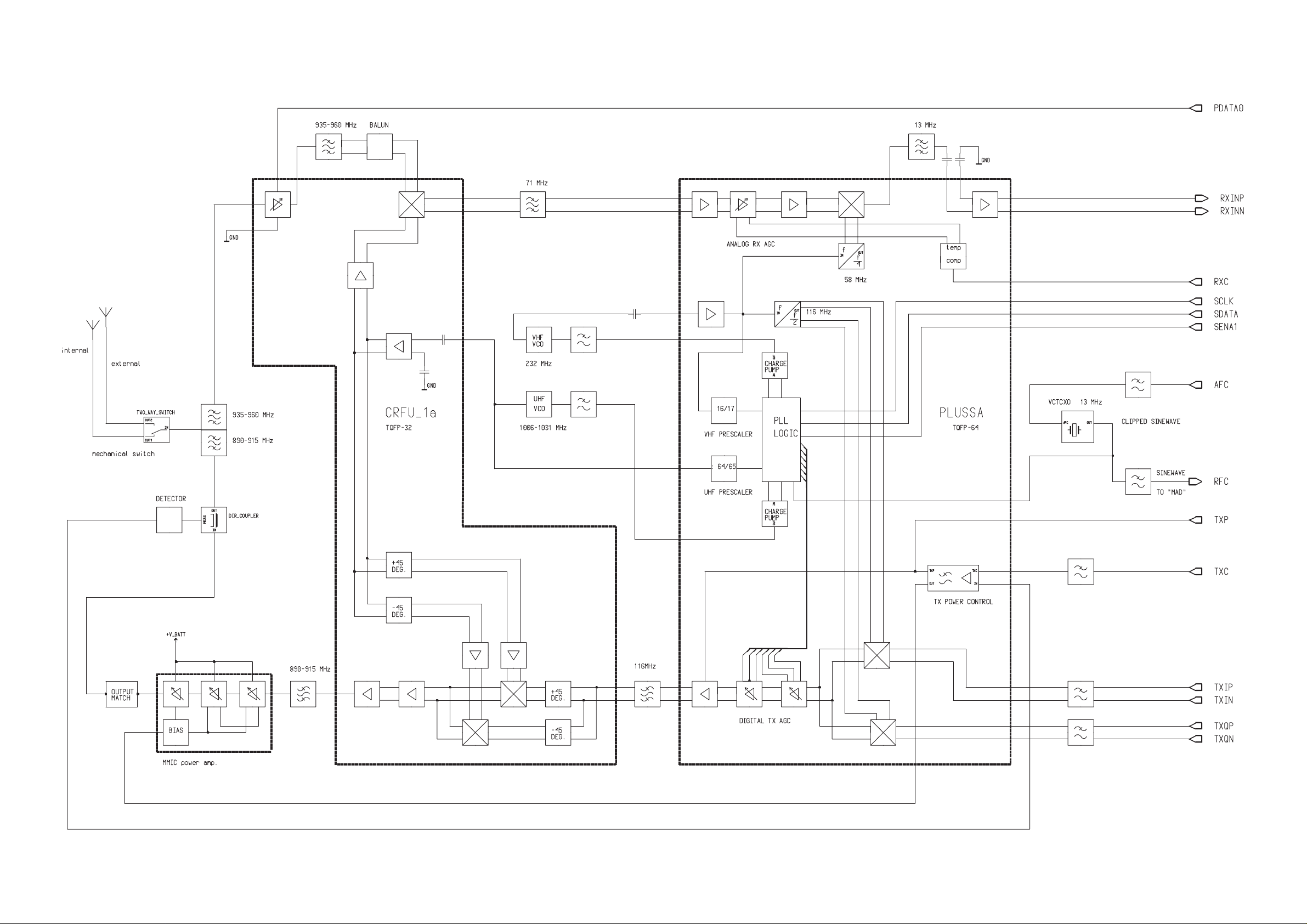
Block Diagram of System/RF Blocks
NSE–3System Module UP8T
Original 11/97
3/A3–1
Page 2
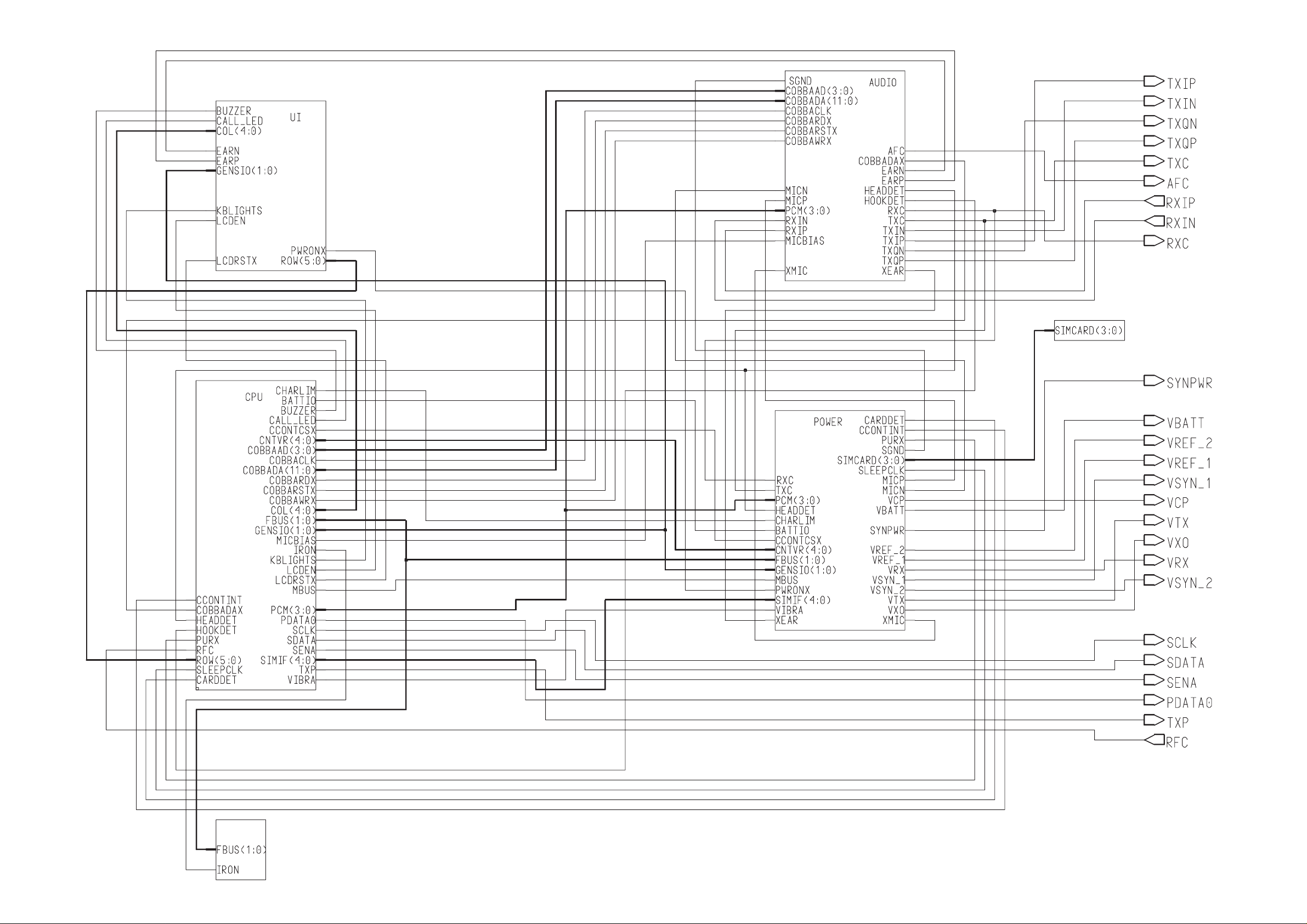
Circuit Diagram of Baseband (Version 12 Edit 8) for layout version 14
NSE–3System Module UP8T
Original 11/97
3/A3–2
Page 3
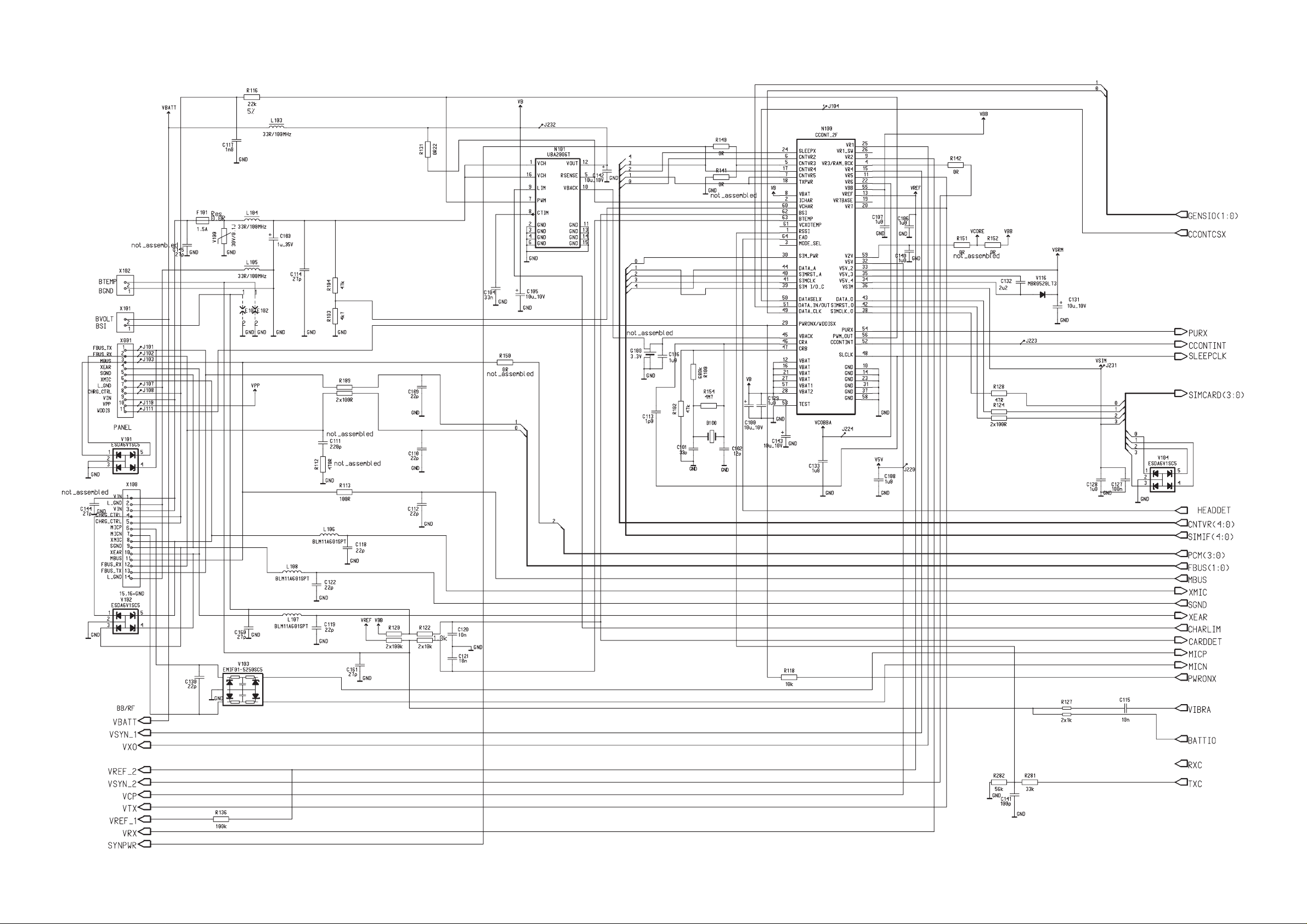
Circuit Diagram of Power Supply (Version 14 Edit 41) for layout version 14
NSE–3System Module UP8T
Original 11/97
3/A3–3
Page 4

Circuit Diagram of SIM Connectors (Version 14 Edit 9) for layout version 14
NSE–3System Module UP8T
Original 11/97
3/A3–4
Page 5

Circuit Diagram of CPU Block (Version 14 Edit 23) for layout version 14
NSE–3System Module UP8T
NSE–3
(NSE–1)
Original 11/97
3/A3–5
Page 6

Circuit Diagram of Audio (Version 14 Edit 27) for layout version 14
NSE–3System Module UP8T
Original 11/97
3/A3–6
Page 7

Circuit Diagram of IR Module (Version 14 Edit 21) for layout version 14
NSE–3System Module UP8T
Original 11/97
3/A3–7
Page 8

Circuit Diagram of RF Block (Version 14 Edit 26) for layout version 14
NSE–3System Module UP8T
Original 11/97
3/A3–8
Page 9

Layout Diagram of UPT8T – Top (Version 14)
NSE–3System Module UP8T
testpoint name condition dc–level ac–level
J102 FBUS_RX power on pulsed DC (0V/2.8V)
J103 MBUS power on pulsed DC (0V/2.8V)
J107 LGND 0V
J110 VPP flash programming nominal 5V (5V flash) or 3.0V
(3V flash)
J111 WDDISX power on reset state 0V, normal state 2.8V
J221 5V flash programming nominal 5.0V (5V flash) or 3.0V
(3V flash)
J222 DSPXF power on pulse active 0V, non–active 2.8V
J229 MAD selftest test mode set externally
J230 MAD selftest test mode set externally
J231 VSIM SIM power on nominal 2.8V (3V SIM card) or
5.0V (5V SIM card)
J232 VB (battery voltage in
baseband)
J233 RFCLK active state typ. 1.0Vpp (min
J234 VSRM power on nominal 5.5V (min 5V, max 6V) CCONT switch
J236 RAMSELX active state pulse active 0V, non–active 2.8V
J250 GND 0V
J252 COBBARSTX power on reset state 0V, normal state 2.8V
J253 COBBAWRX active state pulse active 0V, non–active 2.8V
J254 COBBARDX active state pulse active 0V, non–active 2.8V
J255 COBBACLK active state pulsed DC (0V/2.8V)
battery connected nominal 3.6V (min 3.0, max 4.2)
0.5Vpp, max
2.0Vpp)
mode regulator
ripple voltage
testpoint name condition dc–level ac–level
J502 Power control op.amp
output voltage to N550
( Vpd, pin )
J506 RFC ( 13 MHz sine-
wave )
J510 VRX ( regulated supply
for RX )
J514 VTX ( regulated supply
for TX )
J516 VSYN_1 ( regulated
supply for VCOs)
J518 VREF_2 ( ref. voltage
for N500 )
J520 AFC ( autom. freq. cntrl
)
J522 VXO ( regulated supply
for VCTCXO )
J530
& J532
J540 13 MHz output from
J550 &
J552
J562 RXC ( receive gain
71 MHz IF input to
N620
N620 to Z620
116 MHz TX IF to N500 typ. ca. 1.1 – 1.2 V pulsed typ. ca. 100
control voltage )
power level depended
pulsed DC
0 V typ. 1.0 Vpp min
2.8 V min 2.7 / max 2.85 V,
pulsed
2.8 V min 2.7 / max 2.85 V,
pulsed
2.8 V min 2.7 / max 2.85 V
1.5 V +/– 1.5%
0 – 2.3 V, typ. 1.15 V ( room
temp. )
2.8 V min 2.7 / max 2.85 V
–95 dBm @ X540
(ext. RF connector )
–95 dBm @ X540
(ext. RF connector )
RXC at level of full
calibrated gain
RX gain setting depended control range is 0.5 – 1.45 V,
typ. ca. 1.2 V pulsed typ 100 – 140
typ. ca. 1.5 V pulsed typ. ca. 700
,pulsed.
typ. 1.3–1.4 V for calibrated
maximum gain
0.5/max 2.0 Vpp
uVpp balanced
voltage at 71
MHz
uVrms
mVrms each
Original 11/97
3/A3–9
Page 10

Layout Diagram of UPT8T – Bottom (Version 14)
NSE–3System Module UP8T
testpoint name condition dc–level ac–level
J101 FBUS_TX active state pulsed DC (0V72.8V)
J104 CCONTCSX (CCONT
chip select)
J108 CHRG_CTRL charger connected pulsed DC (0V/2.8V)
J220 V5V active state nominal 5.0V (min 4.8V, max
J223 CCONTINT (charger,
RTC interrupt)
J224 VCOBBA active state nominal 2.8V (min 2.7V, max
J225 EXTSYSRESETX power on reset state 0V, normal state
J226 VCXOPWR power on active state 2.8V, non–active
J227 PURX (power on reset) power up/down reset state 0V, normal state
J228 SLEEPCLK (32kHz
clock)
J235 ROM1SELX active state pulse active 0V, non–active
J251 AGND pcb ground 0V
J256 COBBADAX active state pulse active 0V, non–active
active state pulse active 0V, non–active
2.8V
5.2V)
interrupt pulse active 2.8V, non–active
0V
2.85V)
2.8V
0V
2.8V
power on pulsed DC (0V/2.8V)
2.8V
2.8V
testpoint name condition dc–level ac–level
J500 Control voltage for UHF
VCO module G600
J504 Control voltage for VHF
VCO circuit
J508 VSYN_2 ( regulated
supply for PLLS )
J534&J53613 MHz IF output to
N250
J538 13 MHz output from
Z620 to N620
J542 VHF VCO output ( 232
MHz )
J554 TXC ( TX power control
voltage )
J556 TXP ( TX enable ) 2.8 V logic level pulse,
J558 TXQP ( other half of
balanced Q–signal )
J560 TXIP ( other half of bal-
anced I–signal )
channel 60
channel 1
channel 124
–95 dBm @ X540
(ext. RF connector )
RXC at level of full
calibrated gain
–95 dBm @ X540
(ext. RF connector )
RXC at level of full
calibrated gain
2.25 +/– 0.25 V
> 0.8 V
< 3.7 V
typ. 2.0 –2.2 V min 0.5 / max
4.0 V
2.8 V min 2.7 / max 2.85 V
typ ca. 1.0 – 1.1 V pulsed
min. 0.7 / max. 1.4 V
typ. ca. 1.5 V pulsed typ. ca 600 uVrms
– typ. 400 mVpp.
@level 19 typ. ca. 0.6 V pulse
@level 5 typ ca. 1.8 V pulse
( max. 0.8 V ”0” / min 2.0 V ”1” )
0.8 V pulsed 400 mVpp
0.8 V pulsed 400 mVpp
typ. 50 mVpp balanced
voltage at 13 MHz
> 100 mVpp required
Original 11/97
3/A3–10
 Loading...