

Page 1

Programme’s After Market Services
NME–3 Series Transceivers
JBD–2 User Guide
Issue 1 10/99
Page 2

NME–3
PAMS
JBD–2 User Guide
Technical Documentation
Contents
Introduction 5. . . . . . . . . . . . . . . . . . . . . . . . . . . . . . . . . . . . . . . . . . . . . . . . . . . . . .
Common Functional Description 6. . . . . . . . . . . . . . . . . . . . . . . . . . . . . . . . . . . .
Technical Description 6. . . . . . . . . . . . . . . . . . . . . . . . . . . . . . . . . . . . . . . . . . . . .
Operation Mode TEST 7. . . . . . . . . . . . . . . . . . . . . . . . . . . . . . . . . . . . . .
Operation Mode FLASH 18. . . . . . . . . . . . . . . . . . . . . . . . . . . . . . . . . . . . .
Operation Mode FLS1 19. . . . . . . . . . . . . . . . . . . . . . . . . . . . . . . . . . . . . .
Power Distribution Diagram 19. . . . . . . . . . . . . . . . . . . . . . . . . . . . . . . . . . . . .
Control Unit (EPLD) Description 20. . . . . . . . . . . . . . . . . . . . . . . . . . . . . .
Remote Interface 21. . . . . . . . . . . . . . . . . . . . . . . . . . . . . . . . . . . . . . . . . . . . . .
Page No
Technical Specification 22. . . . . . . . . . . . . . . . . . . . . . . . . . . . . . . . . . . . . . . . . . . .
DC Characteristics 22. . . . . . . . . . . . . . . . . . . . . . . . . . . . . . . . . . . . . . . . . . . .
External Signals and Connections 22. . . . . . . . . . . . . . . . . . . . . . . . . . . . . . .
Abbreviations 27. . . . . . . . . . . . . . . . . . . . . . . . . . . . . . . . . . . . . . . . . . . . . . . . . . . .
Test Sequence of RS232 CTRL–lines 27. . . . . . . . . . . . . . . . . . . . . . . . . . . .
Repair setup 28. . . . . . . . . . . . . . . . . . . . . . . . . . . . . . . . . . . . . . . . . . . . . . . . . .
Flash setup 28. . . . . . . . . . . . . . . . . . . . . . . . . . . . . . . . . . . . . . . . . . . . . . . . . . .
Page 2
Issue 1 10/99
Page 3

PAMS
NME–3
Technical Documentation
JBD–2 User Guide
List of figures
Figure 1. Front Panel Map 6. . . . . . . . . . . . . . . . . . . . . . . . . . . . . . . . . . . . . . .
Figure 2. Rear Panel Map 7. . . . . . . . . . . . . . . . . . . . . . . . . . . . . . . . . . . . . . .
Figure 3. Routed audio path in Test mode 8. . . . . . . . . . . . . . . . . . . . . . . . .
Figure 4. Routed audio path in HS path 9. . . . . . . . . . . . . . . . . . . . . . . . . . .
Figure 5. Routed audio path in HF path 10. . . . . . . . . . . . . . . . . . . . . . . . . . .
Figure 6. Routed audio path in MicSpk 11. . . . . . . . . . . . . . . . . . . . . . . . . . . .
Figure 7. Routed audio path in HF Line 11. . . . . . . . . . . . . . . . . . . . . . . . . . .
Figure 8. Routed audio path in HS test 12. . . . . . . . . . . . . . . . . . . . . . . . . . . .
Figure 9. AMC Circuit 14. . . . . . . . . . . . . . . . . . . . . . . . . . . . . . . . . . . . . . . . . . .
Figure 10. CRM Circuit 15. . . . . . . . . . . . . . . . . . . . . . . . . . . . . . . . . . . . . . . . . .
Figure 11. IGNS Circuit 15. . . . . . . . . . . . . . . . . . . . . . . . . . . . . . . . . . . . . . . . .
Figure 12. PWM Circuit 16. . . . . . . . . . . . . . . . . . . . . . . . . . . . . . . . . . . . . . . . . .
Figure 13. RS232 Test Circuit 17. . . . . . . . . . . . . . . . . . . . . . . . . . . . . . . . . . . .
Figure 14. Old Flash concept 18. . . . . . . . . . . . . . . . . . . . . . . . . . . . . . . . . . . . .
Figure 15. New Flash concept 19. . . . . . . . . . . . . . . . . . . . . . . . . . . . . . . . . . . .
Figure 16. Power Distribution 19. . . . . . . . . . . . . . . . . . . . . . . . . . . . . . . . . . . . .
Figure 17. Simplified Block Diagram of EPLD 20. . . . . . . . . . . . . . . . . . . . . . .
Figure 18. Remote Interface 21. . . . . . . . . . . . . . . . . . . . . . . . . . . . . . . . . . . . . .
Figure 19. Repair setup 28. . . . . . . . . . . . . . . . . . . . . . . . . . . . . . . . . . . . . . . . . .
Figure 20. Flash setup 28. . . . . . . . . . . . . . . . . . . . . . . . . . . . . . . . . . . . . . . . . . .
Issue 1 10/99
Page 3
Page 4

NME–3
PAMS
JBD–2 User Guide
Technical Documentation
[This page intentionally left blank]
Page 4
Issue 1 10/99
Page 5
PAMS
NME–3
Technical Documentation
Introduction
JBD–2 is used to test the NME–3 in the Service Center. It is possible to
use the JBD–2 for testing, analyzing, repairing, and fault logging of the
Radio Unit (RU) and the Handset (HS).
JBD–2 User Guide
JBD–2 is an interface between the phone and the computer when
WinTesla service software is running.
With the JBD–2, it is possible to simulate a normal call, to check all
interfaces are working and to run a final test via WinTesla service
software. The JBD–2 will test all the hardware (HW) interfaces that can
not be checked by using WinTesla.
Issue 1 10/99
Page 5
Page 6
NME–3
PAMS
JBD–2 User Guide
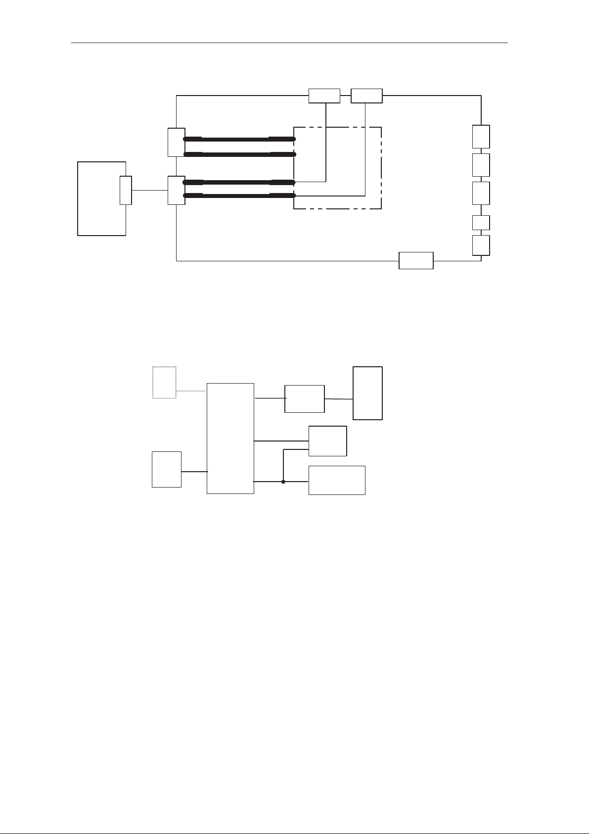
Common Functional Description
In the Test Interface Box (JBD–2), the different audio signal paths are
switched with relays. The actual setting is displayed with LED’s. In
addition the original handsfree equipment can be connected.
Two VDA–signals (IGNS and BLD) will be set from the JBD–2. The AMC
and CRM signals are tested from the JBD–2.
The RS–232 from NME–3 can be tested by using WinTesla together with
RS232 test circuit of the Test Interface Box.
WinTesla communicates with the RU and the HS via the MBUS. The
MBUS is connected tramsparently.
A remote connector optionally controls all settings.
Technical Description
Technical Documentation
AMC
2
VDA–Signals
CRM
IGNS
BLD
100%
OFF
75%
HFMIC
OFF
3 4
RS232–Test /
FLASH_PRG
TEST
FLASH
FLS–1
1
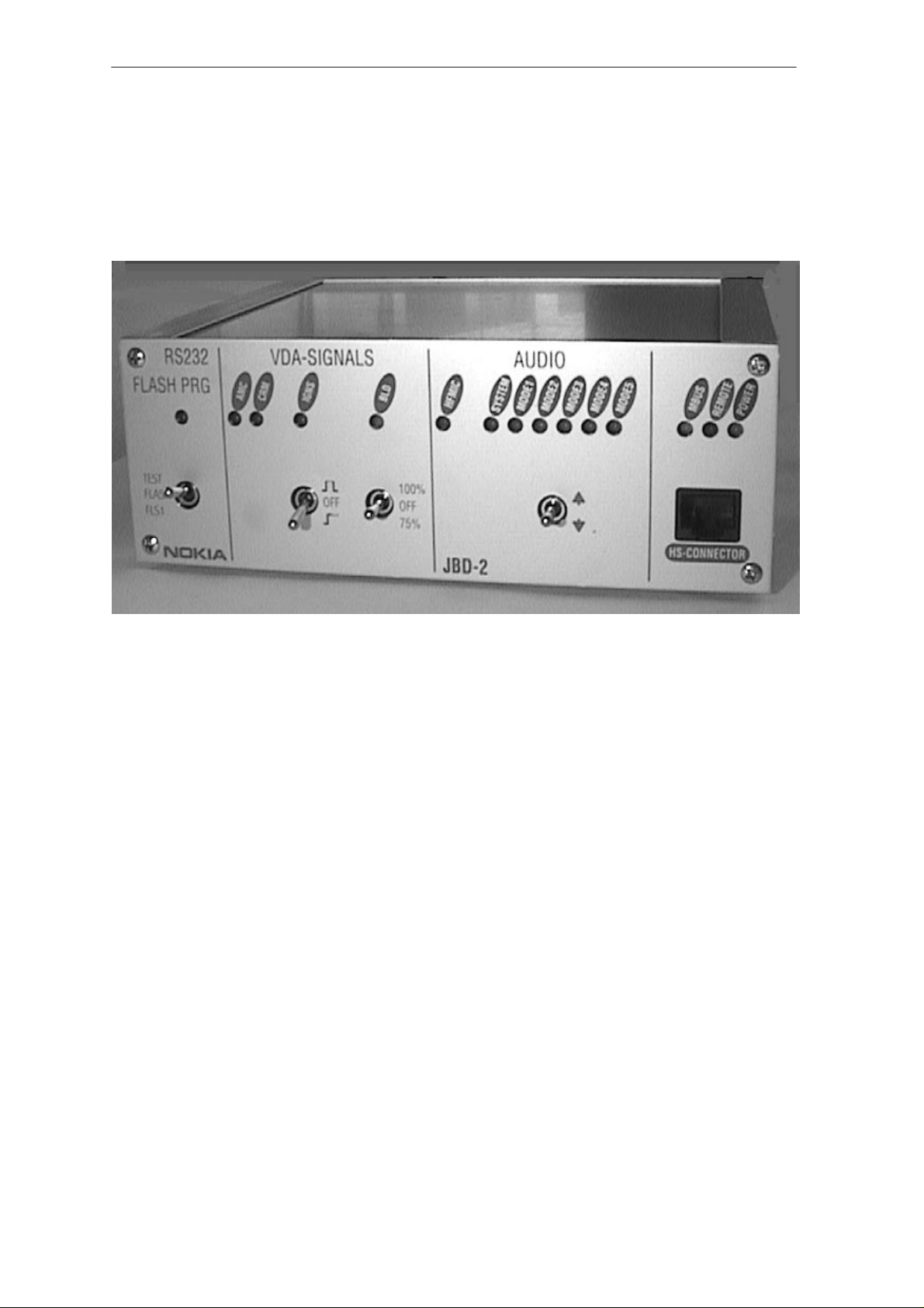
1– Main Switch (testing/flashing) (FLS–1 for future use)
2– Ignition sense (pulsed / off / on)
3– Back light dimming (on / off / 75% brightness = 50% duty cycle
4– DC power for HF mic activen(above &V)
5– Audio path switch
6– HS connector
Figure 1. Front Panel Map
AUDIO
SYSTEM
HSpath
MicSpk
HFpath
HFLine
HStest
MBUS
REMOTE
HS–Connector
POWER
Page 6
Issue 1 10/99
Page 7
PAMS
NME–3
Technical Documentation
JBD–2 User Guide
Modes of Operation
JBD–2 has three operation modes. They are selectable with the switch
(TEST/FLASH/FLS1). The general mode is TEST. In this case, the box is
testing all interfaces from NME–3.
In FLASH mode the JBD–2 support the old FLASH concept and in FLS1
mode the JBD–2 box support the new flash concept with FLS–1
Operation Mode TEST
In this mode, the JBD–2 box together with WinTesla or PCI–/HCI–Test is
able to test all interfaces from NME–3.
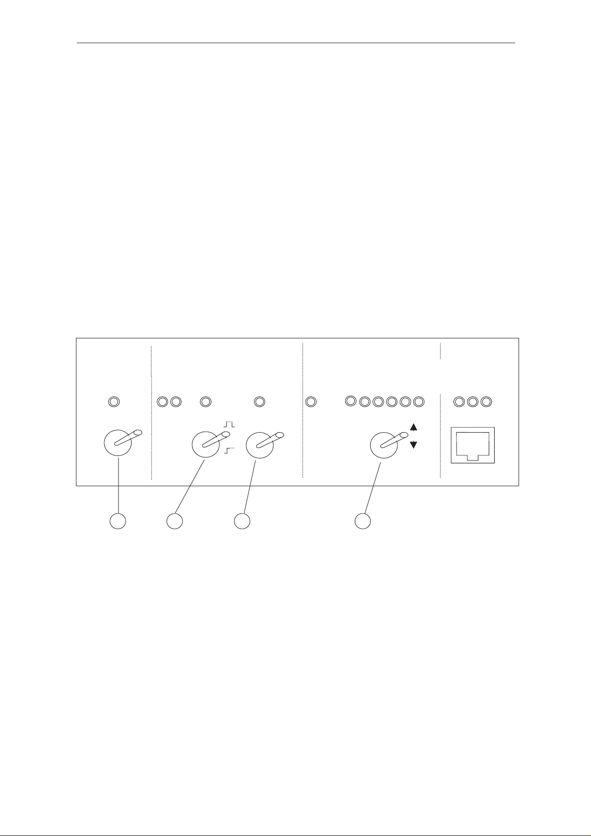
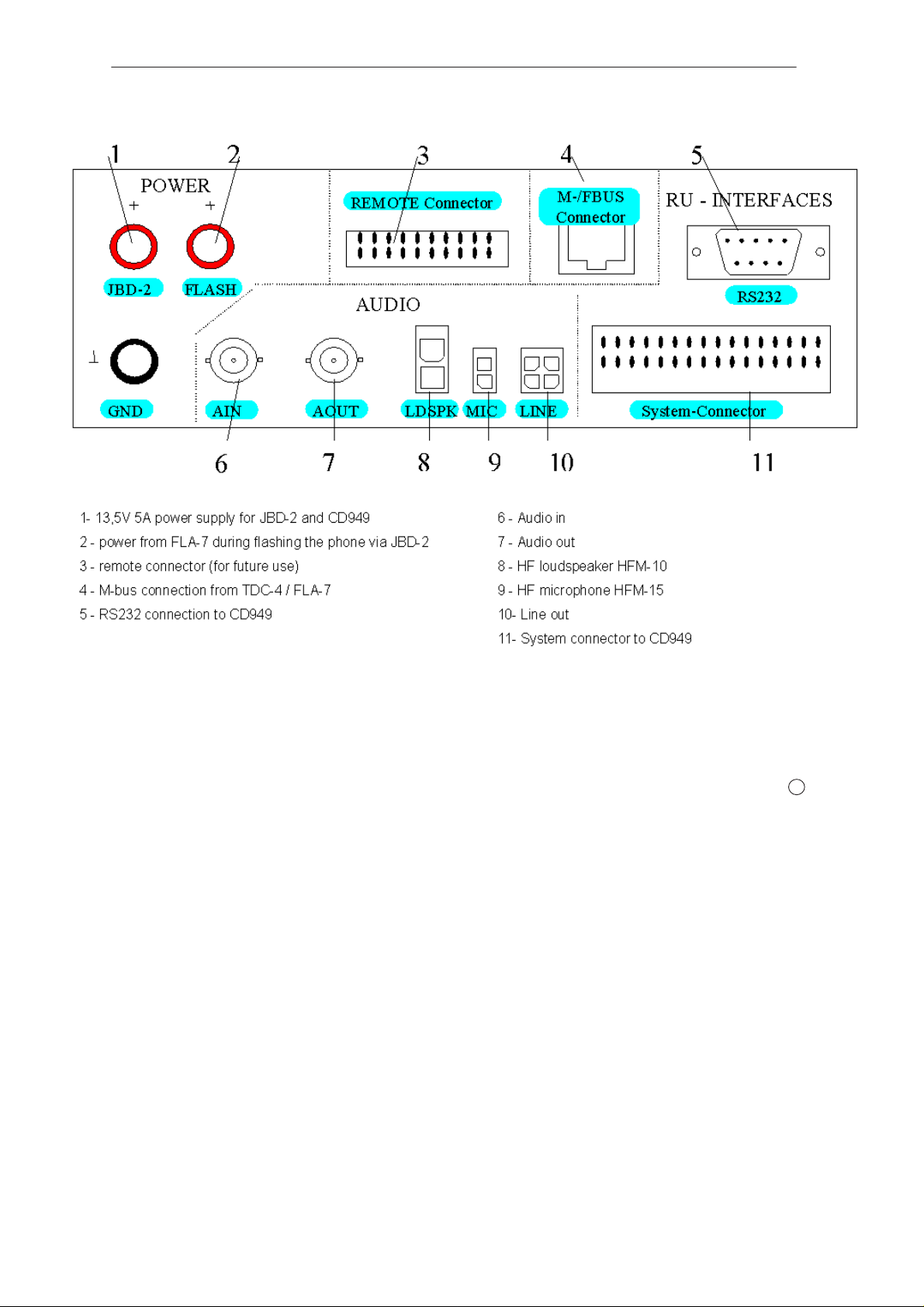
Figure 2. Rear Panel Map
1
Issue 1 10/99
Page 7
Page 8
NME–3
PAMS
JBD–2 User Guide
Possible Audio Test Paths
There are six different audio modes. All audio modes are selectable with
the switch .
Set the switch into the upper position then change the JBD–2 into the
next mode. Switching to the next mode will be indicated by a shift of the
indicator LED one position to right. On the end of the LED line, there is a
wrap around with the next push up.
If you actuate the switch in its bottom position then the JBD–2 will change
into the previous audio mode. On the left end of the LED line, there is a
wrap around with the next push down.
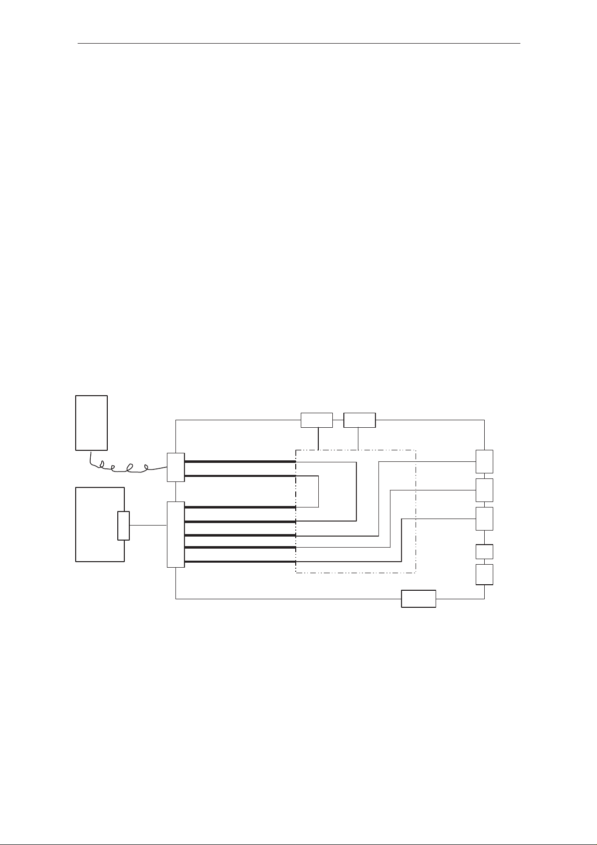
SYSTEM Mode
SYSTEM Mode tests the normal mobile mode.
The audio signals (HSMICP/N & HSEARP/N) will be routed via a matrix to
the handset.
Additionally it will be connecting the following signals HFMICP and
SPKP/N to the handsfree accessories connectors.
Technical Documentation
HS
RU
— These are the default setting after the power–on.
AOUT
HSEARP, HSEARN
HS
HSMICP, HSMICN
HSMICP, HSMICN
HSEARP, HSEARN
HFMICP, HFMICGND
RU
SPKP, SPKN
LINEP, LINEN
AIN
Switch–Matrix
RS232
Figure 3. Routed audio path in Test mode
MIC
SPK
LINE
to PC
Test case
HS path
Page 8
Tests the HS path from the RU.
The audio signals (HSMICP/N & HSEARP/N) are routed via switch matrix
to AIN and AOUT. They are converted with electronics from an
unbalanced to balanced signal and vice versa.
Issue 1 10/99
Page 9
PAMS
NME–3
Technical Documentation
HS
RU
RU
AIN
HSEARP,HSEARN
HSMICP , HSMICN
HSMICP , HSMICN
HSEARP ,HSEARN
Switch–Matrix
Figure 4. Routed audio path in HS path
JBD–2 User Guide
AOUT
MIC
SPK
LINE
to PC
RS232
Test Setup
HS
RU
Measure Application
This describes one of several measure possibilities.
In order to test to the complete HSMIC and HSEAR path, the RU must be
set on internal audio–loop. Then inject a HSMIC signal in AIN and
measure the HSEAR signal with oscilloscope at AOUT.
If it is not possible to set the RU on the internal audio–loop, it is possible
to create it on the RF side with an external audio–loop and a GSM tester.
JBD–2
AOUT
AIN
TDC–4
CH1
CH2
PC
OSCI
Signal
Generator
HF path
Tests the HF path from the RU.
The audio signals (HFMICP& SPKP/N) are routed via switch–matrix to
AIN and AOUT.
— The audio signal SPKP/N is a balanced signal. (A
balanced–to–unbalanced converter is used).
Issue 1 10/99
Page 9
Page 10

NME–3
PAMS
JBD–2 User Guide
RU
Test Setup
HS
RU
AIN
HSEARP,HSEARN
HSMICP , HSMICN
HFMIC
P
SPKP,SPKN
Switch–Matrix
Figure 5. Routed audio path in HF path
Technical Documentation
AOUT
MIC
SPK
LINE
to PC
RS232
Test Application
One of several measuring possibilities is to test the complete audio path
HFMIC–SPK with the help of a signal generator and an oscilloscope. The
RU must be switched into the internal audio loop between the HFMIC path
and the SPK path. The HFMIC signal has to be injected at AIN AC
coupled. Then measure the SPK signal at AOUT with an oscilloscope.
MicSpk
HS
RU
JBD–2
AOUT
AIN
PC
TDC–4
OSCI
CH1
CH2
Signal
Generator
Page 10
MicSpk tests the HF path from the RU with the original accessories.
The audio signals (HFMICP & SPKP/N) are routed via matrix to the
handsfree accessories.
Issue 1 10/99
Page 11

PAMS
NME–3
Technical Documentation
HS
RU
RU
AIN
HSEARP,HSEARN
HSMICP , HSMICN
HFMICP
SPKP ,SPKN
Switch–Matrix
Figure 6. Routed audio path in MicSpk
JBD–2 User Guide
AOUT
MIC
SPK
LINE
to PC
RS232
HF Line
RU
Tests the Lineout path from the RU.
The audio signals LINEP/N&HFMICP are routed via switch matrix to
AOUT and AIN.
HS
RU
HSEARP,HSEARN
HSMICP , HSMICN
HFMICP
LINEP , LINEN
AIN
Switch–Matrix
Switch–Matrix
AOUT
RS232
MIC
SPK
LINE
to PC
Issue 1 10/99
Figure 7. Routed audio path in HF Line
Page 11
Page 12

NME–3
PAMS
JBD–2 User Guide
Test Setup
HS
HS test
Tests the HS path from the HS.
The audio signals (HSMICP/N & HSEARP/N) are routed via switch matrix
to AOUT and AIN where they are converted with to an unbalanced to
balanced signal and vica versa.
RU
JBD–2
AOUT
AIN
Technical Documentation
PC
TDC–4
OSCI
CH1
CH2
Signal
Generator
HS
HS
RU
AIN AOUT
HSEARP,HSEARN
HSMICP , HSMICN
HSMICP , HSMICN
HSEARP , HSEARN
Switch–Matrix
Figure 8. Routed audio path in HS test
MIC
SPK
LINE
to PC
RS232
Page 12
Issue 1 10/99
Page 13

PAMS
NME–3
Technical Documentation
Test Setup
HS
RU
Measure Application
JBD–2
AOUT
AIN
JBD–2 User Guide
PC
TDC–4
OSCI
CH1
CH2
Signal
Generator
The ear path can be tested by injecting a sinusoidal signal to AIN then a
tone can be detected on the HS.
To test the microphone path, inject a tone in the microphone of HS and
measure the signal with oscilloscope at AOUT.
In addition, with an acoustic coupler between ear and microphone in HS
you can estimate the audio HS path with an oscilloscope.
Additional measure applications:
• Set backlight in the HS to 100%, 75% and OFF with MBUS
commands.
³WinTesla creates the MBUS commands.
³The result must be checked visually.
• Keyboard test
1st step: WinTesla sends MBUS commands to HS, which create
characters on HS display.
2nd step: Press the required character on the keyboard manual.
3rd step: WinTesla read the pressed character via MBUS and
compare it with the required character.
• SIM–connector test controlled about WinTesla with MBUS commands
VDA Tests only this must be converted by means of electronics.
The JBD–2 can check four VDA signals. The signals AMC and CRM are
checked permanently. The other signals IGNS and BLD generates the
box. Make these tests only in the audio modes 1–4 and system.
Note : It is important that the power supply is adjusted to 13.5V.
Issue 1 10/99
Page 13
Page 14

NME–3
Á
Á
PAMS
JBD–2 User Guide
AMC
The integrated test circuit checks the line continually, if the signal is active
and it meets the specification, the dedicated green LED will be lit.
RU Connector
VDA Signals
AMC
100 mA
Figure 9. AMC Circuit
On (is lit)
ÁÁÁÁ
Level detection
> 9V
LED–State
Technical Documentation
AMC OK
Explanation
Signal meets the specification.
БББББББББ
(The drive current ~100 mA)
Test Setup
HS
RU
Measure Application
Activate AMC signal with MBUS commands. WinTesla or PCI–Tests create
the MBUS commands.
The indication LED illuminates if the signal meets the VDA specification.
Do not activate AMC into WinTesla or PCI–Test. Then the LED has to be
switched off.
JBD–2
TDC–4
OFF
Signal doesn’t meet the specification.
PC
Page 14
Issue 1 10/99
Page 15

PAMS
Á
Á
Á
Á
NME–3
Technical Documentation
CRM
The line will be observed permanently. If the signal is active and it meets
the specification, a green LED will be lit.
VDA Signals
RU Connector
CRM
120 mA
Figure 10. CRM Circuit
LED State
ON (is lit)
ÁÁÁ
OFF
ÁÁÁ
JBD–2 User Guide
+5V
Level detection
< 0,3V
CRM OK
Explanation
Signal meets the specification; i.e. the level of signal will
БББББББББББББ
be driven at lower than 0,3 V.
Signals don’t meet the specification.
БББББББББББББ
Test Setup
HS
RU
Test Application
In WinTesla or PCI–Test, you can switch on and off the CRM signal. The
dedicated LED will be showing the actual test result. The LED is lit only
when the CRM level is lower than 0,3 V and NME–3 can drive 100 mA to
low114.
IGNS
The signal can be superimposed with a pulse or it can be switched on
continuously. If the signal is activated a green LED will be lit.
PC
TDC–4
JBD–2
OFF
RU Connector
Issue 1 10/99
VDA Signals)
IGNS
+12V
Figure 11. IGNS Circuit
IGNS
LED State
ON (lit)
OFF
Explanation
The signal is active; i.e. the level
of signal is higher than 12V
The signal isn’t active
Page 15
Page 16

NME–3
PAMS
JBD–2 User Guide
Test Setup
HS
RU
Measure Application
Activate the switch, NME–3–RU has to be running.
While the RU is running press the IGNS switch (operates/stroke) for a
short time in the other position, WinTesla will show the changes in a
window.
BLD
Technical Documentation
PC
TDC–4
JBD–2
The signal can be superimposed (supercharged) with fixed values of a
PWM. If the backlight signal is active the green LED (BLD), has to be lit.
• If a handset is available, the test path can be checked visually.
• If no HS is available the converted value can be read from the RU and
compared with the expected value. This is a semi–automatic test.
75%
OFF
100%
BLD
PWM
Generator
VDA Signals
RU Connector
BACKLIGHT
Page 16
Figure 12. PWM Circuit
Note: 100% – maximum brightness
75% -¾ of maximum brightness (conforms a duty cycle with
50%)
Issue 1 10/99
Page 17

PAMS
NME–3
Technical Documentation
Test Setup
HS
RU
Measure Application
With the tappet switch it is possible to inject a specific PWM signal. E.g.,
75% and WinTesla reads the converted signal from NME–3–RU and show
it in the correct window. Check if the signal value meets the expected
value.
RS232 Test
JBD–2 User Guide
PC
TDC–4
JBD–2
Connect to the RS232 interface to test the functionality of the connector. If
Service SW starts the interface test, the test signals pass the Loop
Adapter and will be sent back, if the interface is working correct.
Loop Adapter circuit :
RS232–Test
OFF
ON
RXD
RTS
DTR
CTS DSR CTRL
0X 0
X0 0
11 1
RS232
Connector
TXD, RTS, DSR, DCD, RI
TXD
RXD, CTS, DTR
CTS
DCD
DSR
RI
CTS, DSR
Decoder
Note: CTRL=’l’ DCD,RI connected to CTS,DTR
The test circuit has two possible states. The first state is the ‘
mode and the second condition is the ‘
DSR lines can control the switching between the two modes.
• In the normal–loop mode, the lines RX/TX, RTS/CTS and DSR/DTR
The service software must be regarded that the CTS and the DSR line never take
the logical value ‘1’ at the same time.
Issue 1 10/99
Figure 13. RS232 Test Circuit
can be checked.
advance–loop
normal–loop
’ mode. The CTS and
Page 17
’
Page 18

NME–3
PAMS
JBD–2 User Guide
• In the advance–loop mode check the RI and DCD lines.
The service SW has to ensure care that the lines CTS & DSR are
activate during measurement.
Test Setup
HS
RU
Measure Application
Technical Documentation
PC
TDC–4
JBD–2
RS232
Activate the loop–back test in WinTesla. The test result will be displayed in
a window of WinTesla.
Additionally the RS232 control lines can be tested discretely. This is using
the settings in WinTesla. Test sequence are listed in
”Test Sequences of RS232 CTR–Lines”. at the end of this document.
Operation Mode FLASH
In this case, the switch has to be in the position FLASH and the power
connector “FLASH” must be connected to the service battery cable from
FLA–7.
In addition, the power supply at the power connector “JBD–2” must be
+13.5 V.
HS
JBD–2
MBUS
FLA–7
FPS–4
Dongle
PC
Page 18
RU
TDF–4
Figure 14. Principle old Flash concept
Issue 1 10/99
Page 19

PAMS
NME–3
Technical Documentation
Operation Mode FLS1
In this mode, the NME–3–RU can be reprogrammed with the new flash
concept.
HS
MBUS
JBD–2
RU
Figure 15. Principle new Flash concept
Power Distribution Diagram
JBD–2 User Guide
FLS–1
PC
HS
Connector
RU
Connector
The main operational voltage is +5 and +12V, but the
balanced–to–unbalanced and unbalanced–to–balanced converters need a
special operating voltage: +10V. In the audio mode 5, the power supply of
the handset will be supplied from the JBD–2. The level detection circuits
also need +12V. This is why four voltage regulators are needed.
CTRL_SystemMode
+
V
HS8V
HS8V_RU
CAR12V, CARGND
CTRL_FLASH_Prg
Adj. 8V REG
1 A
TESTBOX
Adj. 12V REG
1 A
Adj. 10V REG
250 mA
Adj. 5V REG
1 A
Verpolungsschutz
+ 1,5A Fuse
+12V
+10V
+5V
The voltage will be controlled via dedicated control lines. The control line
“CTRL13” will be activate if the switch is in its upper (TEST) position.
The control line “CTRL12” will be activated if the audio mode 5 is selected.
Issue 1 10/99
FLASH
JBD–2
Figure 16. Power Distribution
Page 19
Page 20

NME–3
PAMS
JBD–2 User Guide
Control Unit (EPLD) Description
The control unit is implemented with a programmable logic block
Functions of the EPLD:
• PWM Generator of BLD signal
• Handling of all switches on the front panel
• It links the remote control interface with the manual control elements
The EPLD was designed with the “ALTERA MAX+PLUS II” version 9.1 on
a personal computer. The design is hierarchically structured. A big part of
the EPLD circuit design is implemented in schematics and the rest is in
VHDL–scripts and truth tables. The VHDL script is be used to design the
PWM generator of the backlight circuit. The truth–tables are preferential
used for decoders.
Technical Documentation
To
audio mode switch
13kHz
To
BLD switch
To
REMOTE connector
RM_Enable
Scanning of
the Audio
Mode
Switch
RM_Enable
PWM
Generator
Audio mode
Counter with
wraparound
RM_Enable
RM_Enable
Audio mode path
Decoder
Unit to control
the rest of
signals
To
audio path relays
To
BLD transistor
To
the remaining switches
Page 20
Figure 17. Simplified Block Diagram of EPLD
Issue 1 10/99
Page 21

PAMS
ББББББББББББББББ
ББББББ
ББББББ
ББББББ
ББББББ
ББББББ
ББББББ
ББББББББББ
БББББ
БББББ
БББББ
БББББ
БББББ
NME–3
Technical Documentation
Remote Interface
Remote Interface allows all manual adjustments to be controlled. The
results of the VDA measurements (AMC & CRM) and the result of
detecting the DC voltage level in the HFMIC path, are available as output
on the interface.
Use a PC to control the JBD–2 from the IEC–to–Parallel interface.
For example: “ICS 4863 - GPIB Parallel Interface”
JBD–2
Remote connector
ICS 4863
Parallel
IEEE–488
JBD–2 User Guide
PC
Bus Connector
IEC–
Figure 18. Remote Interface
To activate the remote control, the remote line “REMOTE_EN” has to be
set to logical level high (+5V).
The different audio paths can be selected with the three BCD coded
remote lines RM_SYSTEM, RM_MODE1 and RM_MODE2.
Table 2. Significance of the RM_SYSTEM,RM_MODE1,RM_MODE2
RM_MODE2
0
0
0
0
1
1
1
Remote lines
RM_MODE1
0
0
1
1
0
0
1
RM_SYSTEM
0
1
0
1
0
1
X
Selected audio mode
SYSTEM
MODE1
MODE2
MODE3
MODE4
MODE5
reserved
With the input lines RM_FLS1 and RM_TEST will be selected the
differently operating modes of the JBD–2 box.
Table 3. Significance of the RM_FLS1, RM_TEST
Remote lines
RM_FLS1
0
0
1
1
RM_TEST
0
1
0
1
Issue 1 10/99
Selected operating modes
Operating mode FLASH
Operating mode TEST
Operating mode FLS1
reserved
Page 21
Page 22

NME–3
Á
Á
Á
Á
Á
Á
Á
Á
Á
Á
Á
Á
Á
Á
БББББ
Á
БББББ
Á
БББББ
Á
БББББББББББ
Á
БББББ
БББББ
БББББ
БББББББББББ
БББББ
БББББ
БББББ
БББББББББББ
БББББ
БББББ
БББББ
БББББББББББ
БББББ
БББББ
БББББ
БББББББББББ
БББББ
БББББ
БББББ
БББББББББББ
БББББ
БББББ
БББББ
БББББББББББ
БББББ
БББББ
БББББ
БББББББББББ
БББББ
БББББ
БББББ
БББББББББББ
Á
Á
БББББ
Á
БББББ
Á
БББББ
Á
БББББББББББ
Á
БББББ
БББББ
БББББ
БББББББББББ
БББББ
БББББ
БББББ
БББББББББББ
БББББ
БББББ
БББББ
БББББББББББ
БББББ
БББББ
БББББ
БББББББББББ
БББББ
БББББ
БББББ
БББББББББББ
БББББ
БББББ
БББББ
БББББББББББ
БББББ
БББББ
БББББ
БББББББББББ
БББББ
БББББ
БББББ
БББББББББББ
БББББ
БББББ
БББББ
БББББББББББ
БББББ
БББББ
БББББ
БББББББББББ
БББББ
БББББ
БББББ
БББББББББББ
БББББ
БББББ
БББББ
БББББББББББ
БББББ
БББББ
БББББ
БББББББББББ
БББББ
БББББ
БББББ
БББББББББББ
БББББ
БББББ
БББББ
БББББББББББ
Á
Á
БББББ
Á
БББББ
Á
БББББ
Á
БББББББББББ
Á
БББББ
БББББ
БББББ
БББББББББББ
БББББ
БББББ
БББББ
БББББББББББ
PAMS
JBD–2 User Guide
Technical Specification
DC Characteristics
Table 4. Power Supply
Pin / Conn.
БББББ
X21
X21
БББББ
Line Symbol
ÁÁÁÁ
PWR
PWR
ÁÁÁÁ
External Signals and Connections
Pin
ÁÁ
1
2
3
4
5
6
7
8
Line Symbol
БББББ
CAR12V
CARGND
BLD
AMC
FBUSTX
GND
GND
HSPOWER_KEY
Minimum
ÁÁÁÁ
Minimum
ÁÁÁ
13
150
ÁÁÁ
Table 5. System connector (X17)
T ypical /
Nominal
ÁÁÁÁ
Typical /
ÁÁÁ
Nominal
13.5
190
ÁÁÁ
Maximum
ÁÁÁÁ
16
16
Technical Documentation
Maximum
ÁÁÁ
16
300
ÁÁÁ
1.5
ББББББББББ
V /
/ dependent on the connecting device
/ dependent on the connecting device
/ dependent on the connecting device
Unit / Notes
БББББББ
V /
mA / only JBD–2
БББББББ
A / with HS&RU
Unit / Notes
9
ÁÁ
10
11
12
13
14
15
16
17
18
19
20
21
22
23
24
25
ÁÁ
26
27
HSEARP_RU
БББББ
HSEARN_RU
GND
LINEP_RU
LINEN_RU
CAR12V
CARGND
IGNS
CRM
FBUSRX
MBUS
MBUS
HS8V_RU
HSMICP_RU
БББББ
HSMICN_RU
HFMICGND
ÁÁÁÁ
ÁÁÁÁ
ÁÁÁÁ
ÁÁÁÁ
ÁÁÁÁ
16
8
ÁÁÁÁ
ББББББББББ
Not Connected
Not Connected
Not Connected
V /
/ dependent on the connecting device
/ dependent on the connecting device
/ dependent on the connecting device
V /
ББББББББББ
Page 22
Issue 1 10/99
Page 23

PAMS
БББББ
БББББ
БББББ
БББББББББББ
БББББ
БББББ
БББББ
БББББББББББ
БББББ
БББББ
БББББ
БББББББББББ
БББББ
БББББ
БББББ
БББББББББББ
БББББ
БББББ
БББББ
БББББББББББ
Á
Á
Á
Á
Á
Á
Á
Á
Á
Á
Á
Á
Á
Á
Á
Á
Á
Á
Á
Á
Á
Á
Á
Á
Á
Á
Á
Á
Á
Á
Á
Á
Á
Á
Á
Á
Á
Á
Á
Á
Á
Á
Á
Á
Á
Á
Á
Á
Á
Á
Á
Á
Á
Á
Á
Á
Á
Á
Á
Á
Á
Á
Á
Á
Á
Á
Á
Á
Á
Á
Á
Á
Á
Á
Á
Á
Á
Á
Á
Á
Á
Á
Á
Á
Á
Á
Á
Á
Á
Á
Á
Á
Á
Á
Á
Á
Á
Á
Á
Á
Á
Á
Á
Á
Á
Á
Á
Á
Á
Á
Á
NME–3
Technical Documentation
28
29
30
31
32
HFMICP
SPKP_RU
SPKN_RU
Table 6. NME–3 RS–232 interface connector (X25)
Á
1
Á
2
Á
Á
3
Á
Á
4
Á
Á
5
6
Á
7
Á
Á
8
Á
Á
9
Á
Pin
Line
Symbol
ÁÁÁ
DCD
ÁÁÁ
RXD
ÁÁÁ
ÁÁÁ
TXD
ÁÁÁ
ÁÁÁ
DTR
ÁÁÁ
ÁÁÁ
GND
DSR
ÁÁÁ
RTS
ÁÁÁ
ÁÁÁ
CTS
ÁÁÁ
ÁÁÁ
RI
ÁÁÁ
Parameter
ББББББ
Device Carrier Detect
ББББББ
Data Transmit
ББББББ
ББББББ
Data Receive
ББББББ
ББББББ
Data Send Ready
ББББББ
ББББББ
Ground
Data Terminal Ready
ББББББ
Clear T o Send
ББББББ
ББББББ
Ready To Send
ББББББ
ББББББ
Ring Indicator
ББББББ
‘1’
‘0’
‘1’
‘0’
‘1’
‘0’
‘1’
‘0’
‘1’
‘0’
‘1’
‘0’
‘1’
‘0’
‘1’
‘0’
JBD–2 User Guide
Not Connected
Not Connected
Type
Á
ÁÁÁÁÁÁÁÁÁББББББББ
Á
Á
Á
Á
Á
Á
ÁÁÁÁÁ
Á
Á
Á
Á
ÁÁÁÁÁÁÁÁÁББББББББ
Mini–
mum
ÁÁÁ
ÁÁÁ
ÁÁÁ
ÁÁÁ
ÁÁÁ
ÁÁÁ
ÁÁÁ
0
–12
ÁÁÁ
ÁÁÁ
–12
ÁÁÁ
ÁÁÁ
Maxi–
mum
ÁÁ
ÁÁ
ÁÁ
ÁÁ
ÁÁ
ÁÁ
ÁÁ
+12
ÁÁ
ÁÁ
ÁÁ
+12
ÁÁ
ÁÁ
Unit / Notes
ББББББББ
V / dependent on connecting device
V / dependent on connecting device
ББББББББ
ББББББББ
V / dependent on connecting device
ББББББББ
ББББББББ
V / dependent on connecting device
ББББББББ
ББББББББ
V
V / It’s a input
ББББББББ
V / dependent on connecting device
ББББББББ
ББББББББ
V / It’s a input
ББББББББ
ББББББББ
V / dependent on connecting device
Á
Pin
ББББББ
Line
Symbol
1
2
MBUS
3
Á
Á
Á
Issue 1 10/99
HS8V
ББББББ
ББББББ
4
GND
5
HSEARP_HS
6
HSEARN_HS
ББББББ
Table 7. NME–3 Handset interface connector (X1)
Parameter
ÁÁÁÁ
ÁÁÁÁ
ÁÁÁÁ
ÁÁÁÁÁÁÁÁÁÁÁÁÁББББББББББ
Mini–
Á
mum
Á
Á
Typical /
ÁÁÁ
Nominal
8
ÁÁÁ
ÁÁÁ
Maxi–
Á
mum
Á
Á
Unit / Notes
ББББББББББ
Not Connected
V / dependent on the connecting device
V / in MODE5
ББББББББББ
V / in SYSTEM mode depend from
ББББББББББ
NME–3
mV
mV
Page 23
Page 24

NME–3
Á
Á
Á
Á
Á
Á
Á
Á
Á
Á
Á
Á
Á
БББББББББББ
Á
Á
Á
Á
БББББББББББ
Á
БББББББББББ
Á
Á
Á
Á
Á
Á
БББББББББББ
Á
БББББББББББ
БББББББББББ
Á
Á
Á
Á
Á
Á
БББББББББББ
БББББББББББ
Á
Á
Á
Á
Á
Á
Á
Á
Á
Á
Á
Á
Á
Á
Á
Á
Á
Á
БББББББББББ
БББББББББББ
БББББББББББ
Á
Á
Á
Á
Á
Á
Á
Á
Á
Á
Á
Á
Á
Á
Á
Á
Á
Á
Á
Á
Á
Á
Á
Á
Á
Á
Á
Á
Á
Á
PAMS
JBD–2 User Guide
7
Á
Á
Á
HSPOWER_KEY
ББББББ
8
HSMICP_HS
9
HSMICN_HS
10
ББББББ
Pin
Line
ÁÁÁ
Symbol
1
2
SPKP
ÁÁÁ
SPKN
Á
Note: Table1–8, All voltage levels are dependent on the connecting
devices.
Not active
ÁÁÁÁ
Active
ÁÁÁÁÁÁÁÁÁÁÁÁÁББББББББББ
>0,2
Á
0
ÁÁÁÁÁ
0,2
*
Table 8. HF Loudspeaker connector (X14)
Parameter
ББББББ
ББББББÁÁÁÁÁÁÁÁ
Mini–
Á
mum
Typical /
ÁÁ
Nominal
Maxi–
ÁÁ
mum
Technical Documentation
V / *dependent on the connecting device
ББББББББББ
Not Connected
ББББББББББ
V / dependent on the connecting device
ББББББББББ
V / dependent on the connecting device
Unit / Notes
Á
1
2
Á
1
2
Á
Á
Á
3
4
Á
1
Pin
ÁÁÁÁ
HFMICGND
HFMICP
Pin
ÁÁÁÁ
Shield line
LINEN
ÁÁÁÁ
ÁÁÁÁ
ÁÁÁÁ
LINEP
Pin
ÁÁÁÁ
Line
Symbol
Line
Symbol
Line
Symbol
Table 9. HF Microphone connector (X15)
Parameter
БББББ
DC–level
Mini–
mum
Á
900
Typical /
Nominal
ÁÁ
Maxi–
mum
ÁÁ
1100
ББББББББББ
mVRMS / dependent on the connect device
Table 10. LineOut connector (X16)
Parameter
БББББ
Ground
БББББ
БББББ
БББББ
Mini–
Á
mum
900
Á
Á
Á
Typical /
ÁÁ
Nominal
ÁÁ
ÁÁ
ÁÁ
Maxi–
ÁÁ
mum
1100
ÁÁ
ÁÁ
ÁÁ
БББББББББББ
mVRMS / level between LINEN and
БББББББББББ
LINEP is dependent on the
БББББББББББ
connecting device
БББББББББББ
Not Connected
Table 11. M–/ FBUS interface connector (X24)
Parameter
БББББ
Mini–
ÁÁ
mum
Typical /
ÁÁÁ
Nominal
Maxi–
Á
mum
Unit / Notes
Unit / Notes
ББББББББ
Unit / Notes
Not Connected
2
Á
Á
Á
Á
Page 24
ÁÁÁÁÁБББББÁÁÁÁÁÁÁÁÁÁББББББББ
3
GND
4
MBUS
ÁÁÁÁ
5
FBUS_RX
ÁÁÁÁ
6
FBUS_TX
ÁÁÁÁ
Ground
‘1’
БББББ
‘0’
‘1’
БББББ
‘0’
‘1’
БББББ
‘0’
2,25
0
ÁÁ
2,25
0
ÁÁ
2,0
0
ÁÁ
0
3
ÁÁÁ
3
ÁÁÁ
2,8
ÁÁÁ
3,3
0,6
3,3
0,4
3,5
0,6
Á
Á
Á
Not Connected
V
V / dependent on the
connecting devices
ББББББББ
V / dependent on the
connecting devices
ББББББББ
V / dependent on the
connecting devices
ББББББББ
Issue 1 10/99
Page 25

PAMS
Á
Á
Á
Á
Á
Á
Á
Á
Á
Á
Á
Á
Á
Á
Á
Á
Á
Á
Á
Á
Á
Á
Á
Á
Á
Á
Á
Á
Á
Á
Á
Á
Á
Á
Á
Á
Á
Á
Á
Á
Á
Á
Á
Á
Á
Á
Á
Á
Á
Á
Á
Á
Á
Á
Á
Á
Á
Á
Á
Á
Á
Á
Á
Á
Á
Á
Á
Á
Á
Á
Á
Á
Á
Á
Á
Á
Á
Á
Á
Á
Á
Á
Á
Á
Á
Á
Á
Á
Á
Á
Á
Á
Á
Á
Á
Á
Á
Á
Á
Á
Á
Á
Á
Á
Á
Á
Á
Á
Á
Á
Á
Á
Á
Á
Á
Á
Á
Á
NME–3
Technical Documentation
7
Á
Á
Á
Á
Á
Á
Á
Á
Á
Á
Á
Á
Á
Á
Á
Á
CNTRL_A
ÁÁÁÁ
8
CNTRL_B
ÁÁÁÁ
БББББÁÁÁÁÁÁÁÁÁÁББББББББ
БББББÁÁÁÁÁÁÁÁÁÁББББББББ
9
10
Pin
1
2
3
4
5
6
7
8
9
10
11
12
Line
БББББ
Symbol
Parameter
REMOTE_EN
БББББ
GND
RM_IGNS
БББББ
RM_BLD_75
БББББ
RM_BLD_100
БББББ
БББББÁÁÁÁÁÁÁÁÁÁÁÁÁББББББББББ
RM_SYSTEM
RM_MODE1
БББББ
RM_MODE2
БББББ
RM_MODE3
БББББ
RM_MODE4
БББББ
RM_CNTRL_A
БББББ
13
14
RM_CNTRL_B
15
RES_AMC
БББББ
16
RES_CRM
БББББ
БББББ
ÁÁÁ
‘0’
ÁÁÁ
‘1’
Ground
‘0’
ÁÁÁ
‘1’
‘0’
‘1’
ÁÁÁ
‘0’
‘1’
ÁÁÁ
‘0’
‘1’
‘0’
ÁÁÁ
‘1’
‘0’
ÁÁÁ
‘1’
‘0’
ÁÁÁ
‘1’
‘0’
‘1’
ÁÁÁ
‘0’
‘1’
ÁÁÁ
‘0’
‘1’
‘0’
ÁÁÁ
‘1’
‘0’
ÁÁÁ
‘1’
ÁÁÁ
Table 12. Remote connector (X23)
Type
Á
IN
Á
IN
Á
IN
Á
IN
Á
IN
IN
Á
IN
Á
ÁÁÁÁ
ÁÁÁÁ
IN
Á
IN
OUT
Á
OUT
Á
Á
Mini–
ÁÁ
mum
0
ÁÁ
2
0
ÁÁ
2
0
2
ÁÁ
0
2
ÁÁ
0
2
0
ÁÁ
2
0
ÁÁ
2
0
2
0
2
0
2
ÁÁ
0
2
0
ÁÁ
2
0
ÁÁ
2
ÁÁ
Maxi–
ÁÁ
mum
0.8
ÁÁ
5
0.8
ÁÁ
5
0.8
5
ÁÁ
0.8
5
ÁÁ
0.8
5
0.8
ÁÁ
5
0.8
ÁÁ
5
0.8
ÁÁ
5
0.8
5
ÁÁ
0.8
5
ÁÁ
0.8
5
0.8
ÁÁ
5
0.8
ÁÁ
5
ÁÁ
ББББББББББ
V /
ББББББББББ
V / Ignition Sense
ББББББББББ
V / Backlight 75%
ББББББББББ
V / Backlight 100%
ББББББББББ
Not Connected
V / Lines to select the audio modes
ББББББББББ
ББББББББББ
V.../ reserved
ББББББББББ
V.../ reserved
ББББББББББ
V.../
ББББББББББ
Not Connected
V /
V / T est result of
ББББББББББ
AntennaMotorControl
V / T est result of
ББББББББББ
CarRadioMute
ББББББББББ
JBD–2 User Guide
V / dependent on the
connecting device
V / dependent on the
connecting device
Not Connected
Not Connected
Unit / Notes
17
RES_HFMIC
Á
Á
Á
БББББ
БББББ
18
RM_PWRKEY
БББББ
Issue 1 10/99
‘0’
‘1’
ÁÁÁ
ÁÁÁ
‘0’
‘1’
ÁÁÁ
OUT
Á
Á
IN
Á
0
2
ÁÁ
ÁÁ
0
2
ÁÁ
0.8
5
ÁÁ
ÁÁ
0.8
5
ÁÁ
V / Test result of
ББББББББББ
ББББББББББ
V / HSPWR_KEY inactive
––––––– “ –––––––– active
ББББББББББ
BIAS
HF–Microphone
Page 25
Page 26

NME–3
Á
Á
Á
Á
Á
Á
Á
Á
Á
Á
Á
Á
Á
Á
Á
Á
Á
Á
Á
Á
Á
Á
Á
Á
Á
Á
Á
Á
Á
Á
Á
Á
Á
Á
Á
Á
Á
Á
Á
Á
Á
Á
Á
Á
Á
Á
Á
Á
Á
Á
Á
Á
Á
Á
Á
Á
Á
Á
Á
Á
Á
Á
Á
Á
Á
Á
Á
Á
Á
Á
Á
Á
PAMS
JBD–2 User Guide
19
RM_FLS1
Á
Á
Á
Á
ÁÁÁÁ
ÁÁÁÁ
ÁÁÁÁ
ÁÁÁÁ
БББББ
БББББ
БББББ
20
RM_TEST
БББББ
Connector
X12
X13
Connector
X21
X11
Line
ÁÁ
Symbol
AIN
AOUT
Line
Symbol
ÁÁ
PWR
ÁÁ
GND
ÁÁ
Technical Documentation
‘0’
ÁÁÁ
‘1’
ÁÁÁ
ÁÁÁ
‘0’
ÁÁÁ
‘1’
IN
IN
Á
Á
Á
Á
0
ÁÁ
2
ÁÁ
ÁÁ
0
ÁÁ
2
0.8
ÁÁ
5
ÁÁ
ÁÁ
0.8
ÁÁ
5
V /
V /
Lines to select the operating
Á
Á
Á
Á
ББББББББ
mode of JBD–2:
FLASH 00
ББББББББ
FLS1 01
ББББББББ
TEST 10
ББББББББ
Table 13. AIN & AOUT BNC–connectors
Parameter
ББББББ
Mini–
ÁÁ
mum
35
35
Typical /
ÁÁ
Nominal
Maxi–
Á
mum
2500
2500
ББББББББ
mV
mV
Table 14. DC supply connector
Parameter
ББББББ
Power supply input
ББББББ
Ground
ББББББ
Mini–
mum
ÁÁ
13
ÁÁ
Typical /
Nominal
ÁÁ
13,5
ÁÁ
0
ÁÁÁÁÁ
Maxi–
mum
Á
16
Á
ББББББББ
V / Red banana female
connector
ББББББББ
V / Black banana female
ÁÁББББББББ
connector
Table 15. RadioUnit DC Power Supply Connector
Unit / Notes
Unit / Notes
Á
X22
Á
X11
Á
Pin
Line
Symbol
ÁÁÁ
FPWR
ÁÁÁ
GND
ÁÁÁ
Parameter
ББББББ
Mini–
mum
ÁÁ
8
ББББББÁÁÁ
Ground
ББББББ
ÁÁÁÁÁÁ
Typical /
Nominal
ÁÁÁ
13,5
ÁÁÁ
0
Maxi–
mum
Á
16
Á
ББББББББ
V / Red banana female connector
ББББББББ
Unit / Notes
V / Black banana female con-
ÁÁББББББББ
nector
Page 26
Issue 1 10/99
Page 27

PAMS
ББББББ
ББББББ
ББББББ
ББББББ
ББББББ
ББББББ
ББББББ
ББББББ
NME–3
Technical Documentation
Abbreviations
AMC Antenna Motor Control
BLD Backlight Dimming
CRM Car Radio Mute
FLA–7 Flash Loading Adapter
FLS–1 Point of Sale Flash device
FPS–4 Flash Prommer
HS Hand Set
HW Hardware
IGNS Ignition Sense
JBD–2 Test Interface Box
JBD–2 User Guide
PKD–1 Standard Software Dongle
PKD–1CS Central Service Dongle
RU Radio Unit
SCD–2 Repair Place Cable
SW Software
t.b.d. to be defined
TDC–4 ComBox
TDF–4 Security Box
Test Sequence of RS232 CTRL–lines
The following NME–3–Outputs has to set in WinTesla. The NME–3–Inputs
represents the displayed result in WinTesla.
Table 15. Test Sequence of RS232 CTRL–lines
RI
NME–3–Outputs
DCD
X1
X
X
0
0
1
1
X
X
X
0
1
0
1
DSR
CTS
0
0
1
1
1
1
1
NME–3–Inputs
DTR
0
1
0
1
1
1
1
RTS
0
0
1
0
0
1
1
0
1
0
0
1
0
1
DSR DTR
DSR DTR
DSR DTR
RI DTR
RI DTR
RI DTR
RI DTR
Explanation
CTS RTS
CTS RTS
CTS RTS
DCD RTS
DCD RTS
DCD RTS
DCD RTS
Relay state
Inactive
Inactive
Inactive
Active
Active
Active
Active
Issue 1 10/99
Note: 1 the value is not relevant
Page 27
Page 28

NME–3
PAMS
JBD–2 User Guide
Repair setup
Technical Documentation
Flash setup
Figure 19. Repair setup
Page 28
Figure 20. Flash setup
Issue 1 10/99
 Loading...