

Page 1

Programme’s After Market Services
NME–3 Series Transceivers
Troubleshooting
Issue 1 10/99
Page 2

NME–3
PAMS
Troubleshooting
Technical Documentation
CONTENTS
Introduction 3. . . . . . . . . . . . . . . . . . . . . . . . . . . . . . . . . . . . . . . . . . . . .
Radiounit failures 4. . . . . . . . . . . . . . . . . . . . . . . . . . . . . . . . . . . . . . . .
Flashing failures 9. . . . . . . . . . . . . . . . . . . . . . . . . . . . . . . . . . . . . . . .
Phone doesn’t Power On 15. . . . . . . . . . . . . . . . . . . . . . . . . . . . . . . . .
Phone doesn’t Power Off 15. . . . . . . . . . . . . . . . . . . . . . . . . . . . . . . . .
Handset not recognized 15. . . . . . . . . . . . . . . . . . . . . . . . . . . . . . . . . .
Phone doesn’t register to network or phone doesn’t make a call 15
Receiver faults 19. . . . . . . . . . . . . . . . . . . . . . . . . . . . . . . . . . . . . . . . . .
Transmitter faults 29. . . . . . . . . . . . . . . . . . . . . . . . . . . . . . . . . . . . . . . .
AMC not working 47. . . . . . . . . . . . . . . . . . . . . . . . . . . . . . . . . . . . . . . .
Car Radio Mute not working 48. . . . . . . . . . . . . . . . . . . . . . . . . . . . . .
Backlight dimming not working 49. . . . . . . . . . . . . . . . . . . . . . . . . . . .
Audio failure Handsetmode 49. . . . . . . . . . . . . . . . . . . . . . . . . . . . . . .
Audiofailure Handsfreemode 50. . . . . . . . . . . . . . . . . . . . . . . . . . . . . .
Failure in Data interface 50. . . . . . . . . . . . . . . . . . . . . . . . . . . . . . . . . .
SIM–Card not recognized 52. . . . . . . . . . . . . . . . . . . . . . . . . . . . . . . .
Handset failures 55. . . . . . . . . . . . . . . . . . . . . . . . . . . . . . . . . . . . . . . . .
Microphone path fault 59. . . . . . . . . . . . . . . . . . . . . . . . . . . . . . . . . . . .
Earpiece path fault 60. . . . . . . . . . . . . . . . . . . . . . . . . . . . . . . . . . . . . .
LCD fault 61. . . . . . . . . . . . . . . . . . . . . . . . . . . . . . . . . . . . . . . . . . . . . . .
SIM interface fault 61. . . . . . . . . . . . . . . . . . . . . . . . . . . . . . . . . . . . . . .
Keypad fault 63. . . . . . . . . . . . . . . . . . . . . . . . . . . . . . . . . . . . . . . . . . . .
BLD fault 63. . . . . . . . . . . . . . . . . . . . . . . . . . . . . . . . . . . . . . . . . . . . . . .
Hall sensor fault 63. . . . . . . . . . . . . . . . . . . . . . . . . . . . . . . . . . . . . . . . .
Power key fault 63. . . . . . . . . . . . . . . . . . . . . . . . . . . . . . . . . . . . . . . . .
Page 2
Issue 1 10/99
Page 3

PAMS
NME–3
Technical Documentation
Introduction
This document gives a comprehensive guide to NME–3 faultfinding.
NOTE
ules and ensure that:
a) There is no mechanical damages at the units
b) Soldered joints are o.k.
c) check which unit is broken HS or Radiounit
NOTE
umentations. (Power supply connected to the unit, IGNS high, Handset
conneced,...)
The following hints should make it easier to find the cause of the problem
when the product seems to be faulty. This trouble shooting instruction is
divided into the following sections:
: The first thing to do is carry out a through visual check of the mod-
: Make sure that the system is installed as specifided in the AS doc-
Troubleshooting
1. Which Unit is broken
2. RU failures
3. HS failures
Which Unit is broken
To check which unit is broken, the following steps should be performed:
Have a look at the failure describtion, if it doesn’t already indicate which
unit is broken, follow the procedure descibed below:
if there is a handset audio problem, connect the HS to a reference Radiounit and check if the problem is still there.
if the the system is not working at all then follow the steps described below:
– Connect the HS to 8V
– check if the current consumption is O.K.
– check if the Nokia Hands are shown
– If both things are O.K. connect the HS to a reference Radiounit and check if it
works without problems
– In this case it is most likely a Radiounit problem, in all other cases it is most likely
a Handset problem
– Important NOTE: After repair of one unit it allways have to be checked that the
combination of both units is working !!!
Issue 1 10/99
Page 3
Page 4

NME–3
PAMS
Troubleshooting
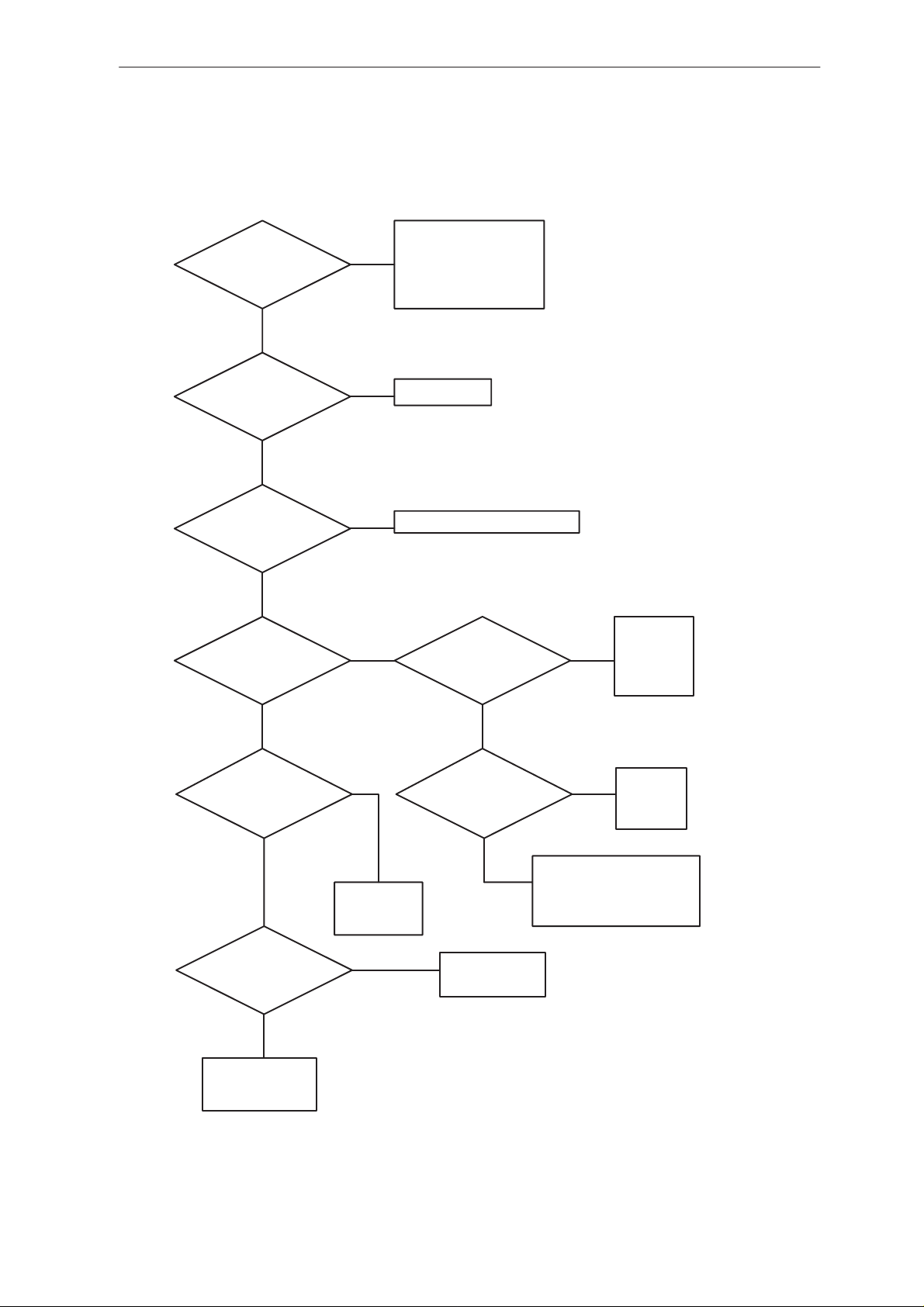
Radiounit failures
This chapter describes how to find failures in the Radiounit:
Radiounit doesn’t Powerup
Connect the Radiounit to +12V while ignition sense is switched off and
look to see if the Leds are turned ON for a short time
– If they don’t turn on at all,
– check the current consumtion, if it is about 300– 400uA the wakeup
logic should be checked, if it is much less or more there is a Problem
in the powersupply
– Check the status of all voltages
– Check the status of the wakeup logic
– If the Leds stay on,
– Check the digital part
Technical Documentation
– Check powerdown logic
– If the LEDs go off as specifed and current is O.K.:
– Try to wakeup the radiounit by turning Ignition sense ON,
– if the Leds stay on go to the next step
– if they don’t stay on or don’t turn on at all check the Ignition circuit
– Try to wakeup the radiounit by pressing the powerbutton of the HS,
– if the Leds stay on go on, try flashing the unit
– if they don’t stay on or don’t turn on at all check the Powerbutton cir-
cuit
Page 4
Issue 1 10/99
Page 5
PAMS
NME–3
Technical Documentation
12V at V1
Yes
12V at C437
Yes
3.8V at C426
No
No
No
Check PCB
fuse, and solderjoints on systemconnector
Check L13
Check N402 and V404
Troubleshooting
Yes
12V at C410
Yes
8V at C415
Yes
8V at C404
Yes
No
No
Check
N401
No
PURX high
D701 Pin 9
Yes
voltage at
C403 =0.7V
No
Check N400
No
Yes
Check
Overvoltagecircuit
Check
wakeup
logic
Check
V400,
V403
Powersupply
O.K.
Issue 1 10/99
Figure 1.
Check the voltages and powersupply
Page 5
Page 6
NME–3
PAMS
Troubleshooting
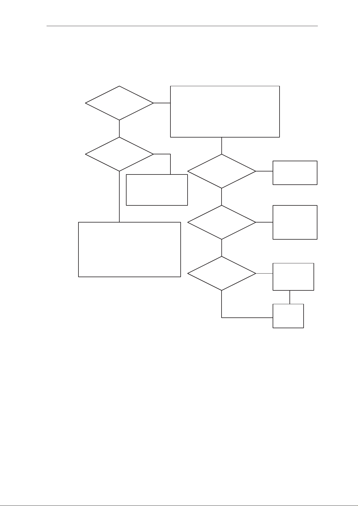
Is Pin 9 of
D702 high
No
Is Pin 13 of
D702 high
Yes
Yes
No
Check circuit on
Pin 13 of D702
Technical Documentation
Disconnect the Powersupply
Connect Probe to Pin 3 of D701
set scope to singletrigger falling edge,
reconnect the powersupply
Scope pic
according
figure 1
Yes
No
Check D701
Check D702
Check that a low pulse is produced
on Pin 10 of D702 when
switching Power On
D701 Pin 9 high
Yes
LEDs on
Yes
No
Check CCONT
No
Check
Powersupply
Check
Digitalpart
Page 6
Figure 2. check wakeup circuit
Issue 1 10/99
Page 7
PAMS
NME–3
Technical Documentation
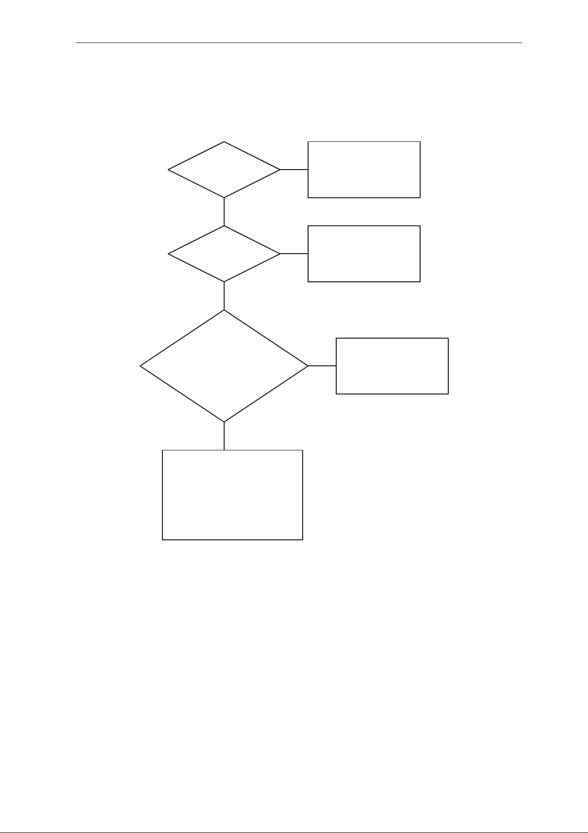
32 Khz
clock on
N700 Pin 48
Yes
13 Mhz
clock on
N700 Pin 48
Yes
No
Check CCONT
and 32Khz oscilator
No
Check VCXO circuit
Troubleshooting
Frequent data from
MAD to CCONT on
CCONT PIN 49–51
No
Check D600.. D603 for
open solder joints
shortcircuits
and broken components
Yes
Try to flash new SW
Issue 1 10/99
Figure 3. check digital part
Page 7
Page 8

NME–3
PAMS
Troubleshooting
D702 Pin 10
high ??
No
Is SW producing a
Powerdown signal
on R721
Check circuit
arround V707
and D702
Technical Documentation
Yes Check circuit connected
to this pin
No
Signal on
R600 low
Yes
Signal on
R603 low
Yes
No
No
check related
circuit
check related
circuit
Try to Flash new
SW
check digital part
Page 8
Figure 4. Check Powerdownlogic
Issue 1 10/99
Page 9

PAMS
NME–3
Technical Documentation
Flashing not possible
The flash programming can be done via system connector X1.
In production, the first programming is done applying 12V flashvoltage to
TP610. In aftersales the Flashvoltage is generated by an on board regulator.
The main differences between production flashing and aftersales flashing
are :
a) FLASH programming voltage is produced in a different way.
b) Signal routings are different.
The fault finding diagrams for production flash programming are shown in
figures 5 and 6.
The fault finding diagrams for aftersales flash programming are shown in
figures 7 and 8.
Troubleshooting
In flash programming error cases the flash prommer can give some information about a fault.
The fault information messages could be:
– MCU doesn’t boot
– Serial clock line failure
– Serial data line failure
– External RAM fault
– Algorithm file or alias ID don’t find
– MCU flash Vpp error
In cases that the flash programming doesn’t succeed there is a possibility
to check short circuits between the memories and the MCU (MAD2).
This test is useful to do, when the fault information is: MCU doesn’t boot,
Serial clock line failure or Serial data line failure.
The test procedure is following:
1. Connect the short circuit wire between the test points J229 and J230.
2. Switch power on to start selftest
3. If the voltage level in D600 PIN 134 is 2.8 V (”1”), the interface is OK. If
there is a short circuit, the voltage level in D600 PIN 134 stays low and
32kHz square wave signal can be seen in the lines which are already
tested.
Selftest behaviour can be seen on the next page.
Note this test can be found only short circuits, not open pins.
Also upper data lines (15:8) of flash circuit D602 are not included to this
test.
Issue 1 10/99
Page 9
Page 10
NME–3
PAMS
Troubleshooting
passed
Technical Documentation
CCONT pin 54
MAD pin 38
MAD pin 134
( PURX )
( MCUAD0)
( ExtSysResX))selftest
Page 10
Issue 1 10/99
Page 11

PAMS
NME–3
Technical Documentation
Production Flash Programming Failure (1)
Flash programming doesn’t work
YES
If the fault information from the prommer is:
a) MCU doesn’t boot
b) serial data line failure
c) serial clock line failure
connect:
connect watchdog disable (WDDIS) line (N700 PIN 28) to ground
OK
EEPROM (D601) Pin 8 (VBB) 2.8V
C706 (VXO) 2.8V
YES
NO
Troubleshooting
See section: Phone is totally dead
check C213, R213
YES
R607 (RFC) 13Mhz
800 mV min
NO
check buffer V300 and
VCXO G300
NO TP700 clock(SCLK)
D701 PIN 9 PURX =”1” 2.8V
YES
NO
MAD2 (D600) pin 93 13 Mhz sine wave
clock signal: 500 mVpp min.
YES
Check that following lines are correct:
FCLK (MBUS) line: X1 pin 22 –> D600 pin 112
FTX (fbus_tx) line: X1 pin 6 ––> D600 pin 104
FRX (fbus_rx) line: X1 pin21 .–>D600 pin 109
check also pullup and pulldown resistors: R606,R614,R617
Check D700, no low signal from N650
OK
Enable the selftest function of D200 by connecting
Voltage level rises to ”1” after power on at D600 Pin 134
D600 PIN 17 to GND
Connect an oscilloscope to D600 PIN 134 and
power on
YES
square wave 32 kHz
YES
Faulty circuit N700
or over loaded PurX line
NO
There is a shortcircuit
somewhere in memory control
lines or MCU address lines or
MCU lower (7:0) data lines
check sleep
NO
clock circuitry
(B701,R707,..)
Issue 1 10/99
There could be open pins in circuits D600 (D602, D603)
If not, the PCB or D600 (D602, D603) is faulty
Figure 5.
Page 11
Page 12
NME–3
PAMS
Troubleshooting
Production Flash Programming failure (2)
Flash progrmming doesn’t work
YES
If the fault information from the prommer is:
External RAM fault
YES
Check pins of SRAM (D603)
Check control lines of SRAM:
RAMSelX ...
Flash progrmming doesn’t work
YES
Technical Documentation
If the fault information from the prommer is:
Algorithm file or alias ID don’t find, ID is unknown etc.
YES
Check pins of FLASH (D602)
Check control lines and upper data lines (15:8)
of FLASH: ROM1SelX...
Flash progrmming doesn’t work
YES
If the fault information from the prommer is:
MCU flash Vpp error
YES
Check connection between TP610 ––> D210; 13
Check components C600, R612, N600, V600
OK
Page 12
Faulty component D602
Figure 6.
Issue 1 10/99
Page 13
PAMS
NME–3
Technical Documentation
Aftersales Flash Programming failure (3)
Flash programming doesn’t work
YES
If the fault information from the prommer is:
a) MCU doesn’t boot
b) serial data line failure
c) serial clock line failure
connect:
connect the shortcircuit wire from N700 pin 29 to Ground (watchdog)
OK
EEPROM (D601) pin 8 (VBB)
C706 (VTX) 2.8V
YES
NO
VBAT is correct
3.8 V
Troubleshooting
YES
N700 is faulty
check C213, R213
YES
R607 (RFC) 13Mhz
800 mV min
NO
check buffer V300 and
VCXO G300
NO C728 sleep clock (SCLK)
D701 Pin 9 PURX = ”1” (2.8V)
YES
NO
MAD2 (D600) pin 93 13 Mhz sine wave
clock signal: 500 mVpp min.
YES
Check that following lines are correct:
FCLK (MBUS) line: X1 pin 22 –> D600 pin 112
FTX (fbus_tx) line: X1 pin 6 ––> D600 pin 104
FRX (fbus_rx) line: X1 pin21 .–>D600 pin 109
check also pullup and pulldown resistors: R606,R614,R617
Check D700, no low signal from N650
OK
Enable the selftest function of D200 by connecting
Voltage level rises to ”1” after power on at D600 Pin 134
D600 PIN 17 to GND
Connect an oscilloscope to D600 PIN 134 and
power on
YES
square wave 32 kHz
YES
Faulty circuit N700
or over loaded PurX line
NO
There is a shortcircuit
somewhere in memory control
lines or MCU address lines or
MCU lower (7:0) data lines
NO
clock circuitry
(B 701, R707)
check sleep
Issue 1 10/99
There could be open pins in circuits D600 (D602, D603)
If not, the PCB or D600 (D602, D603) is faulty
Figure 7.
Page 13
Page 14
NME–3
PAMS
Troubleshooting
Aftersales Flash Programming failure (4)
Flash progrmming doesn’t work
YES
If the fault information from the prommer is:
External RAM fault
YES
Check pins of SRAM (D603)
Check control lines of SRAM:
RAMSelX ...
Flash progrmming doesn’t work
YES
Technical Documentation
If the fault information from the prommer is:
Algorithm file or alias ID don’t find, ID is unknown etc.
Check pins of FLASH (D602)
Check control lines and upper data lines (15:8)
of FLASH: ROM1SelX...
Flash progrmming doesn’t work
YES
If the fault information from the prommer is:
MCU flash Vpp error
YES
Vpp > 3 V in D602 pin 13 (or C600)
YES
Check components C600, R612
OK
NO
YES
Vpp > 3 V in testpoint TP610
YES
Check D601 for bad soldering
NO
Check regulator N600
Page 14
Faulty component D601
Figure 8.
Issue 1 10/99
Page 15

PAMS
NME–3
Technical Documentation
Phone doesn’t Power On
This is described in section 2.2.1
Phone doesn’t Power Off
Press Powerbutton, and check if Powerdown pulse is produced on R 721,
if it isn’t check Powerbutton circuit, if it is produced check circuit around
D702 according to Figure 5.
Set Auto power off to 45 seconds, switch Ignition Off, look if a message
Power will switch of if not used comes up after some seconds. If not
check Ignitionsensecircuit
If yes check if the powerdownpulse is produced on R721, if it is check circuit arround D702 according to figure 2.
If no pulse is produced check the connection from R721 to D600 !!
Handset not recognized
Connect a probe to R606, and check if the line is high and carrying HS
signals, if it check the resistor and the MAD D600.
Troubleshooting
If yes follow the M–Bus signal to the connector.
Phone doesn’t register to network or phone doesn’t make a call
If the phone doesn’t register to the network or the phone doesn’t make a
call, the reason could be either the baseband or the RF part.
The phone can be set to wanted mode by WinTesla service software and
determinate if the fault is in RF or in baseband part (RF interface measurements).
The control lines for RF part are supplied by both the System Asic
(MAD2;D600) and the RFI (Cobba; N800). MAD2 handles digital control
lines ( like synthe, TxP etc.) and Cobba handles analog control lines (like
AFC, TxC etc.).
The DSP software is constructed so that operation states of DSP (MAD2)
can be seen in external flag (DSPXF) output pin (D600 pin 91).
After power up, DSP signals all completed functions by changing the state
of the XF pin (see figure 9 for complete timing and figure10 for detailed
timing).
Issue 1 10/99
Page 15
Page 16
NME–3
PAMS
Troubleshooting
Technical Documentation
1. DSP initialization done
2.Synchronization to network
done
3. Registrarition to network
done.
1 2 3
MAD2 pin 91 (DSPXF)
Figure 9.
Page 16
Issue 1 10/99
Page 17
PAMS
NME–3
Technical Documentation
init
initialize
1
patch code
download
2
dsp
constants
download
initialization
done
Troubleshooting
MAD2 pin 91 (DSPXF)
channel
scan starts
PSW
search last PSW
OK
3
send RACH
RACH OK
go SDCCH
imediate assigment
OK
synchronization
OK
MAD2 pin 91 (DSPXF)
MAD2 pin 91 (DSPXF)
Issue 1 10/99
Figure 10.
Page 17
Page 18
NME–3
PAMS
Troubleshooting
Phone register failure
Phone doesn’t register to the network
Analog supply voltage VCOBBA is >2.7 V
at pin 7,12 ... of Cobba (N800)
Analog reference voltage Vref is 1.5 V
Supply voltage VCP (N700 pin 32) > 4.8 V
Supply voltage VRX (N700 pin 9) > 2.7 V
Supply voltage VSYN_1 (N700 pin 15) > 2.7 V
Supply voltage VSYN_2 (N700 pin 4) > 2.7 V
Supply voltage VTX (N700 pins 11, 20) > 2.7 V
phone doesn,t make a call
or
YES
YES
at pin 9 of Cobba (N800)
YES
during the receiving slot
during the transmitting slot
Check
NO
N700
NO
Check
R800,C800
NO Check
Technical Documentation
N700, D600
YES
Synthesizer lines: SEna (N101 pin 56),
SClk (N101 pin 54)
SData (N101 pin 55)
pulses 0 –> 1 during receiving slot
YES
NO
Check
D600
RF control lines: RxC (N800 pin 18) 0 –> 2.3 Vmax during receiving slot
AFC (N800 pin 19) 0 – 1.2 V typ. during receiving slot
YES
Analog data signal RxIP (N800 pin 22) 0–> 1.5 V DC during receiving slot
Analog data signal RxIN (N800 pin 22) 0–> 1.5 V DC during receiving slot
Used benefit signal is biased to DC and its amplitude is 50 mVpp
nominal and frequency is 13 MHz
YES
NO
DAX signal (N800 pin 48) pulses 1 –> 0 during receiving slot
YES
RF control lines: TxC (N800 pin 17) 0 –> 2.3 Vmax during transmit slot
TxP (D600 pin 176) 0–>1 (2.8 V) during transmit slot
YES
NO
Check
N800
NO
Check
N800 if DC is failed
Check
RF part if benefit signal is failed
Check
N800
Check
NO
N800 if TxC is failed
Check
D600 if TxP is failed
Page 18
Analog data signals: TxIN (N800 pin 13) 0–> 0.8 V DC during transmit slot
TxIP (N800 pin 14) 0 –>0.8 V DC during transmit slot
TxQN (N800 pin 15) 0 –>0.8 V DC during transmit slot
TxQP (N800 pin 16) 0 –>0.8 V DC during transmit slot
Used benefit signal is biased to DC and its amplitude is 300 mVpp
nominal and frequency is 64 kHz
NO
YES
Check
N800
Check
RF part
Issue 1 10/99
Page 19

PAMS
NME–3
Technical Documentation
Receiver faults
This section gives an overview of the strategies used to hunt failures and
defects in the receiver path of the radio unit. Tracking of receiver errors is
best done by following the RX signal path and tracking the signal applied
to the antenna port with a probe and a spectrum analyzer. The following
steps should be done prior to the signal tracking:
– Apply test signal generated by CMD55 to antenna port.
– Set radio unit to local mode with Wintesla.
– Choose RF Controls from Wintesla Testing menu.
– Perform the following settings:
The test signal should then be tracked through the rx signal path by following the procedures given in the figures below.
Troubleshooting
Frequency: 947 MHz
Level: –55dBm
Set RX continuous mode
Set Cont. mode channel 60
Tick front end on.
The RF levels given in the following flow charts were measured with a
Hewlett Packard RF probe. When measuring the levels with a different
probe the resulting levels may be different. The most important thing to
check is wether there is a signal present or not.
Issue 1 10/99
Page 19
Page 20

NME–3
PAMS
Troubleshooting
Receiver Fault (1)
RX
FAULT
Duplexer (Z100)
Ant Pin: –56dBm ?
Yes
Duplexer (Z100)
RX Pin: –59dBm ?
Yes
RX Filter (Z101)
Input: –39dBm ?
Yes
RX Filter (Z101)
Output: –42dBm ?
Yes
No
No
No
No
C135: Check soldering!
If soldering okay:
Change C135!
Z100:Check soldering!
If soldering okay:
Change Z100!
Check Bias of V100!
Vbase = 0.9 V (at R109)
Vcoll = 2.3V (at C115)
Yes
Check soldering of passive
components in LNA
area and change component (V100) if necessary!
Z101: Check soldering!
If soldering is okay
change Z101!
No
Technical Documentation
Check VRX2 (R102):
2.8V
Yes
Check Pdata0 (R100):
2.8V
Yes
Check soldering of passive
components in LNA
area and change component (V100) if necessary!
Check supply of CCONT!
No
No
CCONT (N700)
Check soldering!
MAD (D600):
Check soldering!
Mixer (N100)
RF Input: –44dBm?
1st IF
71MHz
Page 20
Yes
No
C108: Check soldering!
If soldering is okay
change C108!
Issue 1 10/99
Page 21

PAMS
NME–3
Technical Documentation
Receiver Fault (2)
1st IF
71MHz
Mixer (N100)
IF Output: –50dBm
at 71 MHz?
Yes
IF Amp output:
C104
IF signal: –37dBm
at 71 MHz
No
No
Mixer (N100)
RF LO Input:
9dBm at 1018MHz?
Yes
N100: Check soldering!
If soldering is okay
change N100!
Check Bias of V102:
Vbase=0.9V
Vcoll=1.7V
No
No
Troubleshooting
UHF LO
Check soldering of passive
components in IF–AMP
area and change compo-
nents if necessary!
Yes
IF Filter (Z102):
Input: –18 dB
Yes
IF Filter (Z102):
Output: –29 dB
Yes
Plussa (N101):
Pin 51,52: –29 dB
(Single ended)
No
No
No
Yes
C108, C104:
Check soldering!
If soldering is okay
change components!
L101,L102,C109:
Check soldering!
If soldering okay,check for-
short circuits and change
brocken components!
Z102: Check soldering!
If soldering is okay
change Z102!
L104,L105,L107,C110,C111,C1 12,R106:
Check soldering! If soldering okay, check for
short circuits and change brocken components!
Also check Plussa (N101) soldering!
2nd IF
13MHz
Issue 1 10/99
Yes
Page 21
Page 22

NME–3
PAMS
Troubleshooting
Receiver Fault (3)
2nd IF
13MHz
Plussa (N101):
Pin 8: 0dBm at 232
Mhz?
Yes
Plussa (N101):
Pin 44: –3dBm at
13 Mhz?
Yes
No
No No
VHFLO
Plussa (N101):
Pin 47: 2.8V?
Yes
Plussa (N101):
Pin 53: 1.2V?
No
Technical Documentation
Check VRX1 supply volt-
age at CCONT!
Check RXC control voltage
from COBBA (N800)
Pin 18!
Filter (Z103) Input:
–7dBm at 13 MHz?
Yes
Filter (Z103) Output:
–10dBm at 13 MHz?
Yes
Plussa (N101):
Pin 34: –20dBm
Pin35: –16dBm at 13 MHz?
Yes
A
No
No
No
Yes
Change Plussa (N101)!
R116: Check soldering!
If soldering okay, change
component!
Z103: Check soldering!
If soldering okay, change
component!
Plussa (N101):
Pin 34,35: 1.4V DC?
Yes
R114,R112:
Check soldering!
If soldering okay, change
component!
No
Change Plussa (N101)!
Page 22
Issue 1 10/99
Page 23

PAMS
NME–3
Technical Documentation
Receiver Fault (3a)
A
Plussa (N101):
Pin 29,30:
–2dBm at 13 MHz?
Yes
Cobba (N800):
Pin 22,23:
–2dBm at 13 MHz?
No
No
Plussa (N101):
Pin 29,30: 1.2V DC?
Yes
Plussa (N101):
Check soldering!
If soldering okay, change
component!
Check connections
between
Plussa (N101),
Cobba (N800)!
Troubleshooting
Change Plussa (N101)!
No
Yes
COBBA
Issue 1 10/99
Page 23
Page 24

NME–3
PAMS
Troubleshooting
Receiver Fault (4)
COBBA
Cobba (N800):
Pin 7,12,21,25,63: 2.8V
DC?
Yes
Cobba (N800):
Pin 27,53: 2.8V DC?
Yes
No
No
Technical Documentation
Check Cobba voltage!
CCONT Pin 22
Check VBB voltage!
CCONT Pin 55
Cobba (N800):
Pin 9: 1.5V DC?
Yes
Cobba (N800):
Pin 10: 100k load?
Yes
Cobba (N800):
Pin 45:13MHz clock OK?
Yes
Cobba (N800):
Pin 28: “High”?
Yes
Check data and adress lines be-
tween MAD and Cobba(N800)!
If OK, change Cobba (N800)!
No
No
No
No
Check Vref voltage!
CCONT Pin 13
through R253
R800: Check soldering!
If soldering okay,
change component!
Check COBBACLK line
from MAD (D600) Pin144!
Check COBBRSTX line
from MAD (D600) Pin163!
Page 24
Issue 1 10/99
Page 25

PAMS
NME–3
Technical Documentation
Receiver Fault (5)
UHFLO
UHFLO (G301):
Output: –10dBm at
1018 MHz
Yes
No
UHFLO (G301):
Vcc pin: 2.8V DC?
Yes
UHF LO (G301):
VC Voltage (R313)
2.2V at Mid CH?
Yes Yes
Change G301!
No
Check VVCO and R305!
No
Also check Plussa (N101)
Troubleshooting
UHFLO (G301):
Check soldering!
connections!
B
Check bias of V303
Vbase= 0.73V
Vcoll= 7.3V
Yes
Check passive components
in supply and signal path for
soldering and short circuits!
Change defective compo-
nents!
No
Check V8PA (R306):
8V DC?
Yes
Check soldering of V303!
If soldering is OK, change
component!
Check 8V regulator for
No
V8PA!
Issue 1 10/99
Page 25
Page 26

NME–3
PAMS
Troubleshooting
Receiver Fault (5a)
B
UHFLO (G301)
oscillates at any
frequency?
Yes
Plussa (N101):
Pin 21: 13 MHz?
Yes
No
No
Technical Documentation
Change G301!
Check C304
and soldering at Plussa
(N101)!
Plussa (N101):
Pin 9,22,25: 2.8V DC?
Yes
Plussa (N101):
Pin 17,28: 5.0V DC?
Yes
Plussa (N101):
Pin 59: 15k load?
Yes
SCLK, SDATA, SENA
signalling okay?
No
No
No
No
Check VSYN from
CCONT (N700) and
CNTVR3 control from
MAD (D600)!
Check VCP voltage
from CCONT (N700)
Pin 32!
Check soldering at
N101 and R125!
If OK, change R125!
Check SCLK, SDATA,
SENA line from MAD
(D600)!
Change Plussa N101!
Page 26
Yes
Issue 1 10/99
Page 27

PAMS
NME–3
Technical Documentation
Receiver Fault (6)
VHFLO
Plussa (N101):
Pin 18: 2.0V?
Yes
Check soldering of compo-
nents and change defect
components if necessary!
Plussa (N101):
Pin 9,22,25: 2.8V DC?
No
No
Does the VCO oscillate
at any frequency?
Yes
Check VVCO
supply voltage!
No
V301 collector:
2.6V DC?
V301 base:
1.7V DC?
Yes
Yes
Troubleshooting
Check VVCO
No
No
supply voltage!
R311,R319:
Check soldering!
If soldering OK,
change component!
Yes
Plussa (N101):
Pin 17, 25 5V DC?
Yes
Change Plussa (N101)!
No
Check VCP
supply voltage!
V301 emitter:
1.2V DC
Yes
Check V301 and passive
components for soldering
and short circuits!
Change defective
components!
Load at emitter: 330 Ohm
No
If OK, change V301!
V301:
Issue 1 10/99
Page 27
Page 28

NME–3
PAMS
Troubleshooting
Receiver Fault (7)
AFC
RSSI tuning OK?
Yes
Cobba (N800):
Pin 19
between 0.5 ... 2.3V?
Yes
Set Spectrum Analyzer!
Frequency: 13MHz
Span: 10kHz
RESBW:3kHz
No
No
RX Fault
Cobba (N800):
Load at Pin 19:
>1M Ohm?
Change Cobba
Yes
(N800)!
No
Technical Documentation
Check AFC line
for short circuits!
If OK, change Cobba
(N800)!
VCTCXO (G300):
Output frequency
exactly 13MHz?
No
Use Wintesla to set
AFC to MAX!
VCTCXO (G300):
AFC voltage: 2.3V?
Yes
VCTCXO (G300)
Main clock > 13MHz
No
No
Check R302,C305!
If OK, change Cobba
(N800)!
Change VCTCXO
(G300)!
Page 28
Issue 1 10/99
Page 29

PAMS
NME–3
Technical Documentation
Transmitter faults
The following chapter gives an overview of the principles helpful to hunt
errors in the transmit path of the radio unit. The best possibility to look for
the root cause of a transmitter malfunction is to track the transmit signal
through the transmitter path starting at the RF–BB interface to the antenna port.
The following settings should be done using Wintesla prior to the examination of the transmitter path:
– Set radio unit to local mode.
– Choose RF Controls from Wintesla menu.
– Set TX level to TEST.
– Set TX continuos mode.
– Set cont. mode channel 60.
The test signal can now be tracked from the TX–IQ inputs of the Plussa to
the antenna connector.
Note The transmitter should under no circumstances be operated in continuos mode on
any other then the TEST level. If a higher power level is needed for error hunting the
transmitter has to be switched to burst mode.
Troubleshooting
Issue 1 10/99
Page 29
Page 30

NME–3
PAMS
Troubleshooting
Transmitter Fault (1)
TX
FAULT
Plussa (N101) Pin 8:
–2dBm at 232MHz
Yes
Plussa (N101):
Pin 61,62:
–10dBm at 116 MHz
Yes
TXLEV: Test
No
No
Technical Documentation
VHFLO
C
CRFU1A (N200):
Pin 2.3:
–13dBm at 116 MHz
Yes
CRFU1A (N200):
Pin 13:
–10dBm at 1018MHz?
Yes
D
CRFU1A (N200);
No No
Check soldering of R201, R202, L203,
If OK, change defective components!
Load at pin 2,3,
> 1MOhm?
Yes
L203, L201, L202, C203!
UHFLO
No
Check CRFU1A (N200)
pin 2,3 for short circuits!
If OK, change N200!
Page 30
Issue 1 10/99
Page 31

PAMS
NME–3
Technical Documentation
Transmitter Fault (1a)
C
Plussa (N101):
TXQP,TXQN,TXIP,TXIN
okay?
Yes
Plussa (N101):
TXP pulse at Pin 1 OK?
Yes
No
No
Check TXQP,TXQN,TXIP,TXIN
lines from Cobba (N800, pin
13...16) and soldering at Plussa
(N101) and Cobba (N800)!
If OK, change Cobba (N800)!
Check TXP line from MAD (D600)!
Troubleshooting
Note:
For the steps described on this
page the transmitter should be
switched to burst mode!
Power level should be 2!
Plussa (N101):
Pin 63:
VTX pulse OK?
Yes
Plussa (N101):
Pin 11:
TXC pulse OK?
Yes
Plussa (N101):
Pin 58:
VREF: 1.5V DC?
Yes
Plussa (N101):
Pin 59:
load = 15 kOhm?
No
No
No
No
Check VTX supply voltage from
CCONT (N700)!
Check TXC line
from COBBA (N800)!
Check VREF line from
CCONT (N700)!
R125:Check soldering!
If soldering OK,
change component!
Plussa (N101):
Pin 61,62:
0.8V DC?
Issue 1 10/99
Yes
Change Plussa (N800)!
No
Page 31
Page 32

NME–3
PAMS
Troubleshooting
Transmitter Fault (1b)
D
CRFU1A (N200):
Pin 30:
–10dBm at 902 MHz
Yes
TX Fault 1
No
CRFU1A (N200):
Pin 1,29:
2.8V DC?
Yes
CRFU1A (N200):
Pin 16:
1.5V DC?
Technical Documentation
For the steps described on this
page the transmitter should be
switched back to continuos mode!
No
No
Note:
Check VTX supply voltage
from CCONT (N700)!
Check VREF
from CCONT (N700)!
Yes
CRFU1A (N200):
Pin 20:
load = 10kOhm?
Yes
Change CRFU1A (N200)!
No
R205: Check soldering!
If OK, change component!
Page 32
Issue 1 10/99
Page 33

PAMS
NME–3
Technical Documentation
Transmitter Fault (2)
TX Fault 1
TX Filter (Z250):
Input: 6 dBm?
Yes
No
V8PA supply
at C624 OK?
Yes
Check bias of V254:
Vbase =0.75V
Vcollector =5V
For the steps described on this
page the transmitter should be
switched to burst mode!
TX power level should be 2!
No
No
Note:
Check V8PA regulator (N400)
and switching circuit (V253,
S251) for soldering and defective
components!
Check passive components for sol-
dering and defective components!
Troubleshooting
PA (N254):
Input: 4 dBm?
Yes
PA (N254)
Output: 40 dBm?
Yes
E
No
No
Yes
V254: Check soldering!
If soldering okay, change
component!
TX FIlter (Z250):
Check for soldering
and short circuits!
If OK change TX Filter (Z254)!
PA (N254)
Pin 3: 12V DC?
Yes
PA (N254)
Pin 2: TXC Pulse?
Yes
Change P A module (N245)!
No
No
Check VPA connection!
Check C272, C273, C274, C275
for short circuits!
Change defective components!
Power
control
Issue 1 10/99
Page 33
Page 34

NME–3
PAMS
Troubleshooting
Transmitter Fault (2b)
E
Duplexer (Z100)
Output: 39 dBm?
Yes
Antenna port (X240)
Output: 39 dBm?
Yes
Ant connector (X240):
Check for soldering and short circuits!
If okay, change connector (X240)!
No
No
Technical Documentation
Check duplexer (Z100) for solder-
ing and short circuits!
If OK, change duplexer (Z100)!
(C135): Check soldering!
If OK, change component!
Page 34
Issue 1 10/99
Page 35

PAMS
NME–3
Technical Documentation
Transmitter Fault (3)
Power
control
Transmitter OK?
Yes
Plussa (N101):
Pin 11:
TXC pulse OK?
Yes
No
No No
TX Fault
Cobba (N800):
Pin 17
TXC pulse OK?
Yes
R110, R11 1:
Check for soldering
and short circuits!
If OK change defective components!
Troubleshooting
Note:
For the steps described on this
page the transmitter should be
switched to burst mode!
TX power level should be 2!
Check Cobba (N800)
for soldering and short circuits!
If OK, change Cobba (N800)!
Plussa (N101):
Pin 15:
TXC pulse OK?
Yes
OpAmp (N250):
Pin 5:
TXC pulse OK?
Yes
OpAmp (N250):
Pin 10:
LOOP = 2.8V?
Yes
OpAmp (N250):
Pin 8:
LOOP = 8V?
Yes
F
No
No
No
No
Plussa (N101):
Check for soldering
and short circuits!
If OK change Plussa (N101)!
R268, R270, R266, C259:
Check for soldering
If OK change defective component!
Check LOOP signal from
and short circuits!
MAD (D600) Pin 168!
OpAmp (N250):
Pin 9:
1.4V DC?
Yes
Check N250 and supply
(8V at pin 4) for soldering
and short circuits!
If OK, change N250!
No
Check R258, R252, C257, C256
for soldering and short circuits and
change defective components!
Issue 1 10/99
Page 35
Page 36

NME–3
PAMS
Troubleshooting
Transmitter Fault (4)
F
OpAmp (N250):
Pin 6: Picture 12?
Yes
No
Switch (N250):
Pin 1:
Picture 12?
Yes
OpAmp (N250):
Pin 6:
Picture 12?
Yes
Check N250 and supply
(8V at pin 4) for soldering
and short circuits!
If OK, change N250!
No
No
Technical Documentation
Check S250
for soldering and short circuits!
Change components if soldering is
okay!
Check R260, R256, R257, R250,
R255, C 254
for soldering and short circuits and
change defective components!
OpAmp (N250):
Pin 7: Picture 13?
Yes
OpAmp (N250):
Pin 3: Picture 14?
Yes
OpAmp (N250):
Pin 2: Picture 15?
Yes
OpAmp (N250):
Pin 1: Picture 16?
Yes
Check N250 and supply
(8V at pin 4) for soldering
and short circuits!
If OK, change N250!
No
No
No
No
Check N250 and supply
(8V at pin 4) for soldering
and short circuits!
If OK, change N250!
Check R263, R255
for soldering and short circuits and
change defective components!
Detector-
Fault
Check R261, C255
for soldering and short circuits and
change defective components!
Page 36
Issue 1 10/99
Page 37

PAMS
NME–3
Technical Documentation
Transmitter Fault (5)
Detector-
Fault
Diode (V252):
Pin 3: Picture 17?
Yes
Transistor (V251):
Base: Picture 18?
No
No
Transistor (V251)::
Emitter: 8V DC?
Yes
Check R272, R271, C261, R269
for short circuits and soldering!
Change defective components!
PA Module (N254):
Pin 2: 12V DC?
No
Troubleshooting
Check V8PA supply!
No
Check VPA supply!
Yes
Transistor (V251):
Collector: Fig 19?
Yes
Check V250, R253, R254
for short circuits and soldering!
Change defective components!
No
Yes
Check R264, R267, C260, R265,
R262, V252, R259, V261
for short circuits and soldering!
Change defective components!
Check V251
for short circuits and soldering!
Change defective components!
Issue 1 10/99
Page 37
Page 38

NME–3
PAMS
Troubleshooting
Clock Signals
Technical Documentation
Picture 1. COBBACLK – signal
Picture 2. 13 MHz Main clock – signal
Page 38
Issue 1 10/99
Page 39

PAMS
NME–3
Technical Documentation
Synthesizer Signals
Picture 3. SCLK – signal
Troubleshooting
Picture 4. SDATA – signal
Picture 5. SENA1 – signal
Issue 1 10/99
Page 39
Page 40

NME–3
PAMS
Troubleshooting
Transmitter Signals
Technical Documentation
Picture 6. TXQP, TXQN, TXIP and TXIN – signal
Picture 7. TXQP, TXQN, TXIP and TXIN – signal (single burst)
Page 40
Issue 1 10/99
Page 41

PAMS
NME–3
Technical Documentation
Troubleshooting
Picture 8. TXC – signal at Plussa Pin 5, Pin 15
Picture 9. VTX – signal
Issue 1 10/99
Page 41
Page 42

NME–3
PAMS
Troubleshooting
Technical Documentation
Picture 10. Vapc – signal (TXLEV2)
Picture 11. OPAMP (N250) Pin 5
Page 42
Issue 1 10/99
Page 43

PAMS
NME–3
Technical Documentation
Troubleshooting
Picture 12. OPAMP (N250) Pin 6
Picture 13. OPAMP (N250) Pin 7
Issue 1 10/99
Page 43
Page 44

NME–3
PAMS
Troubleshooting
Technical Documentation
Picture 14. OPAMP (N250) Pin 3
Picture 15. OPAMP (N250) Pin 2
Page 44
Issue 1 10/99
Page 45

PAMS
NME–3
Technical Documentation
Troubleshooting
Picture 16. OPAMP (N250) Pin 1
Picture 17. Signal at detector diode input
Issue 1 10/99
Page 45
Page 46

NME–3
PAMS
Troubleshooting
Technical Documentation
Picture 18. Signal V251 base
Picture 19. Signal V251 emitter
Page 46
Issue 1 10/99
Page 47

PAMS
NME–3
Technical Documentation
AMC not working
Switch on the phone, with no
load on the AMC ouput
AMC output
high ?
Yes
Add 150 Ohm Load
to AMC output
AMC output
high ?
No
Ask load from
Yes
costumer
check cableing
highlevel
on R458
Yes
Troubleshooting
No
Check D600
for shortcicuits or
open Joints
No
Check
C451, R455
R459 V453
Follow Levels in
AMC circuit
Figure 11. AMC not working
Issue 1 10/99
Page 47
Page 48

NME–3
PAMS
Troubleshooting
Car Radio Mute not working
Switch on the phone, make a call
with no load
on the CRM ouput
CRM output
low ?
Yes
Add 150 Ohm Load
to CRM output and 12V
CRM output
low ?
No
Ask load from
Yes
costumer
check cableing
highlevel
on R453
Yes
Technical Documentation
No
Check D600
for shortcicuits or
open Joints
No
Check
C450, R451
R454 V45
Follow Levels in
CRM circuit
Figure 12. CRM not working
Page 48
Issue 1 10/99
Page 49

PAMS
NME–3
Technical Documentation
Backlight dimming not working
Apply different Dutycycles
to BLD input
Inverted BLD
at R712 ?
DC Level at C729
follows dutycycle
Check circuit
No
before R712
No
Troubleshooting
Check BLD
circuit
Yes
Check N700 for
bad solderpoints
shortcircuits, or
change CCONT
Figure 13. Backlight dimming not working
Audio failure Handsetmode
Setup a call to a GSM–Tester
If uplink is broken use testbox to feed a audiosignal into the circuit, and
follow the signal to the COBBA.
If it is O.K. till here, check the PCM interface on PIN 49..52 of N800.
Check N800,D600 for broken solderjoints shortcircuits, or change compo-
nents
If downlink is broken send a testsignal from the GSM–Tester to phone
and follow the signal from COBBA till the Connector.
If no signal comes out of N800 check PCM interface and act as decribed
above.
Issue 1 10/99
Page 49
Page 50

NME–3
PAMS
Troubleshooting
If both links are broken, start the investigation on the N800 side as described
Audiofailure Handsfreemode
First steps:
Check that 8V DC are on the HF–Micinput, when no load is connected.
Check that a 4V DC Offset voltage is at the outputs are on N502
PIN 7, PIN8
If not check the Offset voltage generation (R522, N502 )
Check that a 4V DC Offset voltage is at the outputs of N501PIN 1, Pin 7
If not check the Offset voltage generation (R522, N502 )
If these checks are passed make a call to the CMD 55.
Technical Documentation
If there is an uplink failure, feed a signal into the HF–Microphone input,
and follow the signal to N800.
If it is O.k. check N800, D600 and the PCM interface
If there is a downlink failure, send a audio signal from the tester to the
phone, and follow the signal from the Cobba to the outputs for Lineout
and HF speaker.
If no signal comes out of N800 check N800, D600 and the PCM interface
Failure in Data interface
Put the data loopback adapter to the D9 connector and use Win–tesla to
control the RS232 outputpins and read the RS232–Inputs.
Page 50
Issue 1 10/99
Page 51

PAMS
NME–3
Technical Documentation
Pin 26 N650
2.8V ?
Yes
Pin 4 N650
–5V ?
Yes
Pin 27 N650
+5V ?
Troubleshooting
No
Check Z650
No
Check Chargepump
C650..C653, N650
No
Yes
Use Wintesla and Loopbackadapter to set the status of every loop
On and Off. Follow every signal
from the Madoutput to the connector and back from the connector to
the MADinput
Figure 14. Failure in RS232 interface
Issue 1 10/99
Page 51
Page 52

NME–3
PAMS
Troubleshooting
SIM–Card not recognized
Disconnect SIM from
phone, connect probe to
C750
2.8V at
No
C750
Yes
Press SIM.
switch
Yes
0V at
C750
Technical Documentation
Check R751, check C750 and
X750 for Shortcircuits
Check contact of
No
SIM–Reader check
switch
Yes
Put Simcard on Simreader
using Simadapter
SIM
No
recognized ?
Yes
Follow instructions
described in Figure 10
Figure 15.
Put insulated wire to C750,
assemble Bottomenclossure, repeat test using big
SIM–Card to close switch
Page 52
Issue 1 10/99
Page 53

PAMS
NME–3
Technical Documentation
The hardware of the SIM interface from MAD2 (D600) to the SIM connector (X750) can be tested without the SIM card.
You have to close the SIM–Switch by using the SIMCard adapter with a
SIM–Card. When the power is switched on, the Sim interface is started
once at 3V and once at 5V. Check with a storage osciloscope, that
VSIM,RSTand DATA rise up to 3V and 5V for some short time, and that
there is 3V/5V Clocksignal on the Clock Pin. To Trace the signals you
should switch the phone on and off several times.
Thus ”Insert SIM card” faults can be found without SIM card.
The fault information ”Card rejected” means that ATR message (the first
message is always sent from card to phone) is sent from card to phone
but the message is somehow corrupted, data signal levels are wrong etc.
or factory set values (stored to the EEPROM) are not correct.
Troubleshooting
Issue 1 10/99
Page 53
Page 54

NME–3
PAMS
Troubleshooting
SIM Card failure
VSIM(36), DATAO(43),SIMRSTO(42) and SIMCLKO(38) lines
rises up to 3/5 V after power on at pins of N100 (CCONT)
SIMPWR(30), DATAA(44), SIMRST A(40), SIMCLK(41) and SIMIOC(39) lines
Insert SIM card fault
YES
Voltage level < 1.5 V
NO
at pin 95 of D600 when
YES
VSIM, DATA, RESET and CLOCK lines
rises up to 3/5 V after power on at pins
Check
R751,C750,X750
YES
of SIM card
NO
YES
NO
rises up to 2.8 V after power on at pins of N700 (CCONT)
NO
Technical Documentation
Check
SIM card and SIM reader
connectors
Check
X750, R709, R710, C730
C731, V703
YES
faulty circuit
N700 (CCONT)
SIMCardPwr(129), SIMCardData(120), SIMCardRstX(127), SIMCardClk(126) and SIMCardIOC(128) lines
rises up to 2.8 V after power on at pins of D600 (MAD2)
NO
Check again that voltage level at pin 95 (SIMCardDetX) of D600 is lower than 1.5V
If it is, change D600
Card Rejected fault
YES
VSIM is according the specification
VSIM = 2.8 V min (with 3 V SIM card)
NO
faulty circuit
N700 (CCONT)
VSIM = 4.5 V min (with 5 V SIM card)
YES
The ATR data can be seen at pin 43
(CCONT, N700)
YES
The ATR data can be seen at pin 120
(MAD2, D600)
YES
SIMIOControl line (N700 pin 36) is ”1”
during the ATR message
NO
NO
NO
Check
X750, R710
Check
N700
Check
D600
YES
faulty PCB
Page 54
YES
Check D600
Issue 1 10/99
Page 55

PAMS
NME–3
Technical Documentation
2 Handset failures
This section describes faults by active components and trace defects,
serial resistances, interconnections etc..
When you get a defective HS then first connect the HS to 8V and check if
the Nokia hands are shown in the display. In this case you can be sure
that main parts of the HS are running (MCU and oscillator, 5V and 3V
power supply, reset circuit, LCD circuit), if not go to section 3.1.
If no further information is shown on the LCD when connected to the reference RU, then there is a problem with the HS MBUS circuit, goto section 3.2.
When there is some further information on the LCD when connected to
the reference RU you can be sure that the MBUS circuit is working and
you can go to other failures like
1. Audio failure
2. LCD failure
Troubleshooting
3. Sim Interface failure
4. Keypad failure
5. Backlight dimming failure
6. Hall sensor failure
7. Power key failure
These are described separately at the end of the section
Issue 1 10/99
Page 55
Page 56

NME–3
PAMS
Troubleshooting
HS general fault
HS general
fault
8V supply ok?
Limits 7.5V – 8.0V
C106
Yes
5V supply ok?
Limits 4.8–5.2V
C113
Yes
No
No
Check Curly–Cord
Check V100
Yes
Check N100
Technical Documentation
No
Change V100
No
Change N100
3V supply ok?
Limits 2.8–3.2V
C124
Yes
Measure Pin 3 /
N101 if High
Limits 4.5–5.0V
Yes
Measure Pin 4 /
N102 if High
Limits 4.8–5.0V
No
No
No
Change N103
Measure Pin 2 /
N101 if Low
Limits 0–0.5V
Yes
Change N101
Change N102
No
Change V101
Next Page
Page 56
Issue 1 10/99
Page 57

PAMS
NME–3
Technical Documentation
Continue
Yes
Check oscillator
Pin 77 / D300
Scope 14.6–14.8 MHz
Yes
Check RAM D301
connections to MCU
Yes
Troubleshooting
No
Change crystal B300
No
Change RAM D301
Change MCU D300
Issue 1 10/99
Page 57
Page 58

NME–3
PAMS
Troubleshooting
MBUS fault
Connect the Handset to a Radiounit and switch on the equipment. Between the MBUS messages are times without datatransfer consider these
measurements.
MBUS fault
Yes
Check MBUS communicatiom
at R302
Yes
Check MBUS communication
at R307
No
No
Change Curly–Cord
Change V300
Technical Documentation
Receive–Path and
Transmit–Path
Receive–Path
Yes
Check MBUS communication
Check MBUS communication
at R305
Yes
at R305 and R302
parallel
Yes
Change MCU D300
No
No
Change MCU D300
Change V301
Transmit–Path
Transmit–Path
Page 58
Issue 1 10/99
Page 59

PAMS
NME–3
Technical Documentation
Audio fault
1 Microphone path fault
For checking the microphone path connect the handset to an radiounit
and connect this equipment to an power supply and an CMD55. Set the
CMD55 for audio in the echomode and make a speech test.
With a microphone path fault the first step is to check the microphone,
therefore change the complete microphone and boot and then check the
microphone path again.
If it doesn‘t work check the complete microphone amplifier stage.
Micamp fault
Yes
Check 2.5V supply
at L202
Limits 2.3–2.7V
No
Troubleshooting
Change N201
Yes
Sinus at the
input T207/208
uin=30mVRMS
Check signal at C235/253
u=21mVRMS
+/–3dB
Yes
Sinus at the
input T207/208
Check signal at R218/R229
u=790mVRMS
+/–3dB
Yes
Sinus at the
input T207/208
Check signal at Pin 8/9 X1
u=790mVRMS
+/–3dB
Yes
Change Curly–Cord
No
Check the input path
No
Change OP N202
No
Check the output path
Issue 1 10/99
Page 59
Page 60

NME–3
PAMS
Troubleshooting
Earpiece path fault
For checking the earpiece path connect the handset to an radiounit and
connect this equipment to an powersupply and an CMD55. Set the
CMD55 for audio in the echomode and make a speech test.
With an earpiece path fault the first step is to check the earpiece resistance is between 26 and 36 ohms. If not then change the complete B–cover with earpiece. Then check the earpiece path again.
Earamp fault
Yes
Sinus at the
Wetern–Plug Pin 5/6
Check Pin 5/6 X1
uin=500mVRMS
Yes
Technical Documentation
No
Change Curly–Cord
Sinus at the
Wetern–Plug Pin 5/6
Check signal at C201/C220
u=500mVRMS
+/–2dB
Yes
Sinus at the
Wetern–Plug Pin 5/6
Check signal at Pin 5/8 N200
u=2000mVRMS
+/–2dB
Yes
Sinus at the
Wetern–Plug Pin 5/6
Check signal at X200
u=500mVRMS
+/–2dB
No
Check the input path
No
Change N200
No
Check the output path
Page 60
Issue 1 10/99
Page 61

PAMS
NME–3
Technical Documentation
LCD fault
If there is an LCD fault first check what kind of failure it is. If there are
missing lines or rows, missing pixels or permanently on pixels you have to
change the LCD module, because these failures are related to the module itself.
When you connect the HS to 8V power supply and there are no Nokia
Hands on the display you have to perform the following steps.
LCD fault
Troubleshooting
Nokia Hands ok?
SIM interface fault
For testing of the SIM interface use the Wintesla and also the HCI functions of the Handset. You can use these functions to switch on the 3V and
5V power supply for the SIM interface and to set the SIM_CLK and
SIM_data line to low and high level.
If you don‘t have the possibility to set the HCI functions (R&D software)
you can only test the functionality of the SIM–door switch by WinTesla
and the general power supply for the SIM card.
No
Check SCLK at pin 2 and
SDIN at pin 4 of D401
Yes
Check SCLK at pin 18 and
SDIN at pin 16 of D401
No
No
Change MCU (D300)
Change D401
When you get a Handset with SIM failure first connect it to an RU and put
in a Test–SIM, to check if SIM switch is working. If SIM card is not recognized the failure is related to the SIM switch, otherwise to the rest of the
SIM interface.
Before error hunting also check the mechanics of the SIM reader and the
SIM door for damage or dirt on the contacts. After this goto the following
procedure.
Issue 1 10/99
Page 61
Page 62

NME–3
PAMS
Troubleshooting
SIM fault
Check 3V power
supply at C401 (lim-
its 2.8V to 3.2V)
Yes
No
Check 3V power supply at
C400 (limits 2.8V to 3.2V)
Yes
Check voltage of gate V401
limits 0V to 0.5V
Yes
No
No
Technical Documentation
Check voltage at basis of
V400 (limits 0V to 0.5V)
for 3V
Yes
Change V400
Change MCU D300
Check 5V power
supply at C400 (lim-
its 4.8V to 5.2V)
Yes
Change D400
By no reaction
Change MCU D300
No
Change V401
Check voltage at basis of
V400 (limits 0V to 0.5V)
for 5V
Yes
Change V400
No
Change MCU D300
Page 62
Issue 1 10/99
Page 63

PAMS
NME–3
Technical Documentation
Keypad fault
First check with WINTESLA which keys are not working. Then change
keymat and repeat test. If anything is ok keymat was defective otherwise
check connections from MCU to keypad matrix.
If all connections are ok check diodes and pullup resistors for keypress
interrupt. If ok change the MCU (D300).
BLD fault
First check which kind of failure you have, is complete keypad and/or
LCD illumination not working or only a part of the illumination not working.
If complete keypad illumination is not working measure voltage at base
(Pin2/V422). If voltage is approximately 4.4V then change V422, if not
change MCU D300.
If complete LCD illumination is not working measure voltage at base
(Pin2/V423). If voltage is approximately 4.4V then change V423, if not
change MCU D300.
Troubleshooting
If only one part of the keypad or LCD illumination is not working check the
3 diodes of the common part.
Hall sensor fault
For checking the hall sensor connect the handset to an radiounit and connect this equipment to an powersupply and an CMD55. Setup a call. Then
check the handset and the handsfree mode via the cradle. If the audio
switch handset/handsfree is working then change the cradle.Also check
the level at the hallsensor output N400 is low when the handset is in the
cradle. If not change the hallsensor. Is the hallsensor working then
change the MCU D300.
Power key fault
When the power key is not working first check the curly cord. If curly cord
is ok change power key button else check the passive hardware circuit.
Issue 1 10/99
Page 63
 Loading...