

Page 1

Programmes After Market Services
NME–3 Series Transceivers
Technical Information
Issue 1 10/99
Page 2

NME–3
Technical Information
Technical Documentation
CONTENTS
Introduction 5. . . . . . . . . . . . . . . . . . . . . . . . . . . . . . . . . . . . . . . . . . . . . . . . . . . . . .
Powerdown Mode: 5. . . . . . . . . . . . . . . . . . . . . . . . . . . . . . . . . . . . . . . . . . . .
Idle Mode 5. . . . . . . . . . . . . . . . . . . . . . . . . . . . . . . . . . . . . . . . . . . . . . . . . . . .
normal mode 5. . . . . . . . . . . . . . . . . . . . . . . . . . . . . . . . . . . . . . . . . . . . . .
timer mode 5. . . . . . . . . . . . . . . . . . . . . . . . . . . . . . . . . . . . . . . . . . . . . . . .
Call Mode 5. . . . . . . . . . . . . . . . . . . . . . . . . . . . . . . . . . . . . . . . . . . . . . . . . . . .
HF voice call 5. . . . . . . . . . . . . . . . . . . . . . . . . . . . . . . . . . . . . . . . . . . . . . .
HS voice call 5. . . . . . . . . . . . . . . . . . . . . . . . . . . . . . . . . . . . . . . . . . . . . .
Data call 5. . . . . . . . . . . . . . . . . . . . . . . . . . . . . . . . . . . . . . . . . . . . . . . . . .
Power Distribution 6. . . . . . . . . . . . . . . . . . . . . . . . . . . . . . . . . . . . . . . . . . . . . . . .
PAMS
Page No
Protection Circuits 8. . . . . . . . . . . . . . . . . . . . . . . . . . . . . . . . . . . . . . . . . .
Power Supply – Handset 9. . . . . . . . . . . . . . . . . . . . . . . . . . . . . . . . . . .
External Signals and Connections 10. . . . . . . . . . . . . . . . . . . . . . . . . . . . . . . . . .
System Connector 10. . . . . . . . . . . . . . . . . . . . . . . . . . . . . . . . . . . . . . . . . . . . .
Data Connector 11. . . . . . . . . . . . . . . . . . . . . . . . . . . . . . . . . . . . . . . . . . . . . . .
Internal Signals and Connections 15. . . . . . . . . . . . . . . . . . . . . . . . . . . . . . . . . . .
SYS Conn Block Conections 17. . . . . . . . . . . . . . . . . . . . . . . . . . . . . . . . . . . .
Audio Block Connections 17. . . . . . . . . . . . . . . . . . . . . . . . . . . . . . . . . . . . . . .
Audio Connection to Handset 17. . . . . . . . . . . . . . . . . . . . . . . . . . . . . . . . . . .
Handsfree Audio Path 19. . . . . . . . . . . . . . . . . . . . . . . . . . . . . . . . . . . . . . . . .
Handset Audio Path 20. . . . . . . . . . . . . . . . . . . . . . . . . . . . . . . . . . . . . . . . . . .
Handsfree Loudspeaker 21. . . . . . . . . . . . . . . . . . . . . . . . . . . . . . . . . . . . . . . .
Handsfree Microphone 21. . . . . . . . . . . . . . . . . . . . . . . . . . . . . . . . . . . . . . . . .
Specification for microphone input 21. . . . . . . . . . . . . . . . . . . . . . . . . . . .
Transceiver (NME–3) 28. . . . . . . . . . . . . . . . . . . . . . . . . . . . . . . . . . . . . . . . . . . .
Baseband 28. . . . . . . . . . . . . . . . . . . . . . . . . . . . . . . . . . . . . . . . . . . . . . . . . . . .
Functional Description 28. . . . . . . . . . . . . . . . . . . . . . . . . . . . . . . . . . . . . .
Page 2
CCONT for CD949 29. . . . . . . . . . . . . . . . . . . . . . . . . . . . . . . . . . . . . . . . .
Handset interface 33. . . . . . . . . . . . . . . . . . . . . . . . . . . . . . . . . . . . . . . . . .
Multiplexing the Busses 33. . . . . . . . . . . . . . . . . . . . . . . . . . . . . . . . . . . . .
SIM Card in RU 33. . . . . . . . . . . . . . . . . . . . . . . . . . . . . . . . . . . . . . . . . . . .
Power up/Power down procedure 33. . . . . . . . . . . . . . . . . . . . . . . . . . . .
Description of the Brownout circuit 36. . . . . . . . . . . . . . . . . . . . . . . . . . . .
RF 40. . . . . . . . . . . . . . . . . . . . . . . . . . . . . . . . . . . . . . . . . . . . . . . . . . . . . . . . . .
Maximum Ratings 40. . . . . . . . . . . . . . . . . . . . . . . . . . . . . . . . . . . . . . . . . .
Power Distribution 40. . . . . . . . . . . . . . . . . . . . . . . . . . . . . . . . . . . . . . . . . .
Issue 1 10/99
Page 3

PAMS
NME–3
Technical Documentation
Functional Description 42. . . . . . . . . . . . . . . . . . . . . . . . . . . . . . . . . . . . . .
Receiver Characteristics 46. . . . . . . . . . . . . . . . . . . . . . . . . . . . . . . . . . . .
Receiver Module Specification 47. . . . . . . . . . . . . . . . . . . . . . . . . . . . . . .
Transmitter Characteristics 51. . . . . . . . . . . . . . . . . . . . . . . . . . . . . . . . . .
Sub Block Description/Tables 52. . . . . . . . . . . . . . . . . . . . . . . . . . . . . . . .
Synthesizer 57. . . . . . . . . . . . . . . . . . . . . . . . . . . . . . . . . . . . . . . . . . . . . . . .
Antenna 60. . . . . . . . . . . . . . . . . . . . . . . . . . . . . . . . . . . . . . . . . . . . . . . . . . .
Handset (RTE–2HJ) 61. . . . . . . . . . . . . . . . . . . . . . . . . . . . . . . . . . . . . . . . . . . . .
Power up/Power down procedure HS 61. . . . . . . . . . . . . . . . . . . . . . . . .
D.C. Characteristics 61. . . . . . . . . . . . . . . . . . . . . . . . . . . . . . . . . . . . . . . .
External Signals and Connections 63. . . . . . . . . . . . . . . . . . . . . . . . . . . .
Functional Description 63. . . . . . . . . . . . . . . . . . . . . . . . . . . . . . . . . . . . . .
Cradle (CRD–8)) 66. . . . . . . . . . . . . . . . . . . . . . . . . . . . . . . . . . . . . . . . . . . . . . . . .
System Description 66. . . . . . . . . . . . . . . . . . . . . . . . . . . . . . . . . . . . . . . . . . . .
Technical Information
Cradle Concept 66. . . . . . . . . . . . . . . . . . . . . . . . . . . . . . . . . . . . . . . . . . . .
List of Figures
Figure 1. Power Supply Block Diagram 6. . . . . . . . . . . . . . . . . . . . . . . . . . . .
Figure 2. Power Supply Blockdiagram 9. . . . . . . . . . . . . . . . . . . . . . . . . . . . .
Figure 3. Signals and Connections 15. . . . . . . . . . . . . . . . . . . . . . . . . . . . . . . .
Figure 4. CD 949 System overview 16. . . . . . . . . . . . . . . . . . . . . . . . . . . . . . . .
Figure 5. Digital interface in GM8B 17. . . . . . . . . . . . . . . . . . . . . . . . . . . . . . . .
Figure 6. HS audio interface 18. . . . . . . . . . . . . . . . . . . . . . . . . . . . . . . . . . . . . .
Figure 7. Audio Paths for Hands–Free 19. . . . . . . . . . . . . . . . . . . . . . . . . . . . .
Figure 8. Audio Path – Hand–Set 20. . . . . . . . . . . . . . . . . . . . . . . . . . . . . . . . .
Figure 9. Write cycle timing. 29. . . . . . . . . . . . . . . . . . . . . . . . . . . . . . . . . . . . . .
Figure 10. Regular Startup 34. . . . . . . . . . . . . . . . . . . . . . . . . . . . . . . . . . . . . . . .
Figure 11. Invalid wakeup (ignored) 35. . . . . . . . . . . . . . . . . . . . . . . . . . . . . . .
Figure 12. SW crash + Restart 35. . . . . . . . . . . . . . . . . . . . . . . . . . . . . . . . . . .
Figure 13. Regular Shutdown 36. . . . . . . . . . . . . . . . . . . . . . . . . . . . . . . . . . . . .
Figure 14. Brownout procedure total powerdrop 37. . . . . . . . . . . . . . . . . . . . .
Figure 15. Power distribution diagram 41. . . . . . . . . . . . . . . . . . . . . . . . . . . . .
Figure 16. Block diagramm of the CD949 GSM RF part 43. . . . . . . . . . . . . .
Figure 17. RF frequency plan 43. . . . . . . . . . . . . . . . . . . . . . . . . . . . . . . . . . . . .
Figure 18. Phase locked loop , PLL 46. . . . . . . . . . . . . . . . . . . . . . . . . . . . . . .
Figure 19. Power distribution diagram 62. . . . . . . . . . . . . . . . . . . . . . . . . . . . .
Issue 1 10/99
Page 3
Page 4

NME–3
Technical Information
Technical Documentation
A3 Schematics/Layouts
Radio Unit GM8B_06 A–1 – A20. . . . . . . . . . . . . . . . . . . . . . . . . . . . . . . . . . . .
Handset A–21– A28. . . . . . . . . . . . . . . . . . . . . . . . . . . . . . . . . . . . . . . . . . . . . . .
Radio Unit GM8B_07 A–29 – A47. . . . . . . . . . . . . . . . . . . . . . . . . . . . . . . . . .
Note: In printed manuals all A3 drawings are located at the back of the binder
PAMS
Page 4
Amendment 11/99
Page 5

PAMS
NME–3
Technical Documentation
Introduction
The CD949 has 3 Basic Operating Modes, divided into submodes:
Powerdown Mode:
In powerdown mode the complete system is switched off, it is not in
service and consumes a minimum of current.
Idle Mode
normal mode
In idle mode the phone is switched on and in service (if inside network
coverage).
timer mode
When Ignition is switched off the phone goes in to timermode. This means
that the phones stays in idlemode for a specified time and switches itself
off if no action from the user takes place.
Technical Information
Call Mode
HF voice call
Handsfree voice call
HS voice call
Handset voice call
Data call
Receive transmit data
Issue 1 10/99
Page 5
Page 6

NME–3
Technical Information
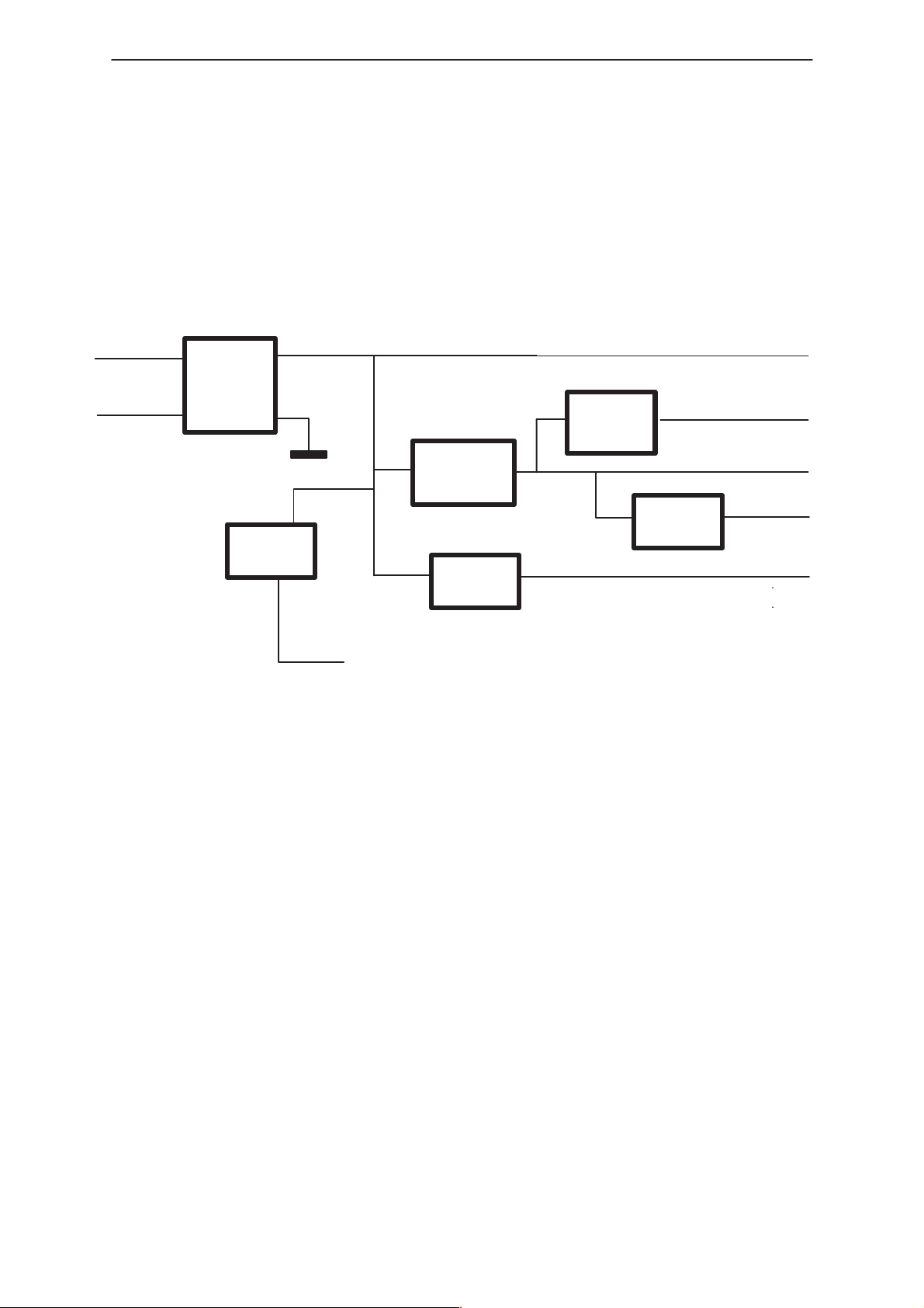
Power Distribution
Power is supplied to the system via the System–Cable or SCM5 (longer
one). The Figure below shows an overview of Power Supply and
Protection Circuits
Carbat+
Carbat–
PowerOn
LineFilter
TVS
Si Switch
&
Aux
Protect
Technical Documentation
12V Supply
8V
Regulator
8V Supply
PAMS
Supply
Monitor
Figure 1. Power Supply Block Diagram
Table 1. Supply Voltages and Power Consumption
Pin / Conn. Line Symbol Minimum Typical /
1/System
17/System
VBATT 0
VBATT 1.5
LoPower
Regulator
_OVERVOLTAGE
_POWERF AIL
_POWERCRITICAL
Nominal
5
10.8
16
13.5
150
Feedback
Maximum Unit / Notes
5
10.8
16
28
4
500
1
Post–Regulator /
LoPower Bypass
V/ no operation
V/ reduced operation
V/ nomal operation
V/ no Operation
A Callmode
mA Idle mode
mA Powerdown mode
3.8V Supply
Page 6
Issue 1 10/99
Page 7
PAMS
NME–3
Technical Documentation
Table 2. External Signals
Pin / Conn. Line Symbol Minimum Typical /
Nominal
11/System Ignition 9
3/System Backlightdimming 9
4/System Antenna motor
control
20/System Car radio mute
21/System FBUS Rx
5/System FBUS Tx
0
13%
60
V–BATT–1 VBATT
9
13.5 16
13.5 16
1
Technical Information
Maximum Unit / Notes
V / ON
0.6
100%
100
0.3
100
0.3
V–BATT
V / OFF
V / High voltage
% / Duty Cycle
Hz / Frequency
V / ON
V / OFF
mA/ Current
V / Voicecall active
V / inactive
kW / external pullup
resistance
23/System MBUS Handset
22/System MBUS Test/Flash
28/System HFMic 92 843 mVrms
32/System HF P 234 2828 mVrms
31/System HF N 234 2828 mVrms
14/System Line out P 70 2000 mVrms
13/System Line out N 70 2000 mVrms
9/System HSEar N 28 802 mVrms
10/System HSEar P 28 802 mVrms
26/System HSMicN 87 790 mV Microphone –
to
microphone +
25/System HSMicP 87 790 mV Microphone +
to
microphone –
8/System HS Powerbutton
1/Data DCD +/– 3.3 +/– 15 V/ inactive
V /active
2/Data Received Data
(output)
+/– 3.3 +/–15 V / binary state 1
V / binary state 0
3/Data transmitted data
(input
4/Data DTR +/– 3.3 +/– 15 V / inactive
5/Data GND 0 V/ reference
6/Data DSR +/– 3.3 +/– 15 V / inactive
+/– 3.3 +/– 15 V/ binary state 1
V/ binary state 0
V / active
ground
V/ active
Issue 1 10/99
Page 7
Page 8

NME–3
Technical Information
PAMS
Technical Documentation
Table 2. External Signals (continued)
MinimumLine SymbolPin / Conn.
Nominal
7/Data RTS +/– 3.3 +/– 15 V / inactive
8/Data CTS +/– 3.3 +/– 15 V / inactive
9/Data RI +/– 3.3 +/– 15 V / inactive
Unit / NotesMaximumTypical /
V/ active
V/ active
V/ active
Protection Circuits
Power is first filtered and protected agains Voltages>30V and Reverse
Voltage. The Supply Monitor switches off the 12V Supply via Si–Switch at
supply Voltages > 16.25V. Aux–Protect clamps peak pulses that are not
covered by the Supply Monitor. Three signals are provided to detect
different supply–voltage levels by other hard– and software:
_OVERVOLTAGE is active at >16.25V, _POWERFAIL at <10,9V.
_POWERCRITICAL is active at a drop of more than 5% on 3.8V Supply. A
LowPower Regulator is used for sleep power for CCONT and MAD.
Three different Voltages are used in CD949. 3.8V for CCONT
(VBCCONT), 8V for RF–PREAMP, AUDIO and for VBCCONT
Regulator,HS and 12V for RFPA, Audio PowerAmp. 12V and 8V can be
switched by PowerOn and automatically by _OVERVOLTAGE.
Page 8
Issue 1 10/99
Page 9
PAMS
NME–3
Technical Documentation
Power Supply – Handset
Power is supplied to the HS via cable from RU. The Figure below shows
an overview of Power Supply and Reset Circuits.
8V
LineFilter
GND
Supply
Monitor
5V
Regulator
3V
Regulator
FIL TER
Technical Information
8V Backlightdiming
5V Audio
5V Digital
RESET
Generator
_RESOUT
3V
SUPPLOWINT
Figure 2. Power Supply Blockdiagram
Issue 1 10/99
Page 9
Page 10
NME–3
Technical Information
External Signals and Connections
CD949 has three external connectors:
– System Connector
– Data Connector
– RF Connector
System Connector
Table 3. External Signals
PAMS
Technical Documentation
Pin / Conn. Line Symbol Minimum Typical /
Nominal
19/System Ignition 9
0
3/System Backlightdimming 9
13%
60
4/System Antenna motor con-
trol
20/System Car radio mute
21/System FBUS Rx
5/System FBUS Tx
23/System MBUS Handset
22/System MBUS Test/Flash
28/System HFMic 92 843 mVrms
31/System HF P 234 2828 mVrms
32/System HF N 234 2828 mVrms
9 VBATT
9
13.5 16
13.5 16
1
Maximum Unit / Notes
V / ON
0
100%
100
0.3
100
0.3
16
V / OFF
V / High voltage
% / Duty Cycle
Hz / Frequency
V / ON
V / OFF
mA/ Current
V / Voicecall active
V / inactive
kW / external pullup
resistance
14/System Line–out P 70 2000 mVrms
13/System Line–out N 70 2000 mVrms
9/System HSEar N 28 802 mVrms
10/System HSEar P 28 802 mVrms
25/System HSMicP 87 mV Microphone +
to
microphone –
26/System HSMicN 87 mV Microphone –
to
microphone +
Page 10
Issue 1 10/99
Page 11
PAMS
NME–3
Technical Documentation
Technical Information
Data Connector
The CD949 transceiver unit GM8B has 3 digital interfaces between the
MAD and external devices. These are the data or RS232 interface, to use
the transceiver as modem. The handset interface used for communication
between the radiounit and the handset, and the Test and Flash interface,
needed for production and after sales purposes. All of these interfaces are
implemented using the M– and F–Bus coming from the MAD.
Table 4. Data interface Spec RS 232
Signal
name
RS232
DCD
RS232TXOutput +– 3,3V .. 15V PIN 2 RS 232 interface for dataaplications and remo-
RS232RXInput +– 3,3V .. 15V PIN 3 RS 232 interface for dataaplications and remo-
RS232
DTR
Signal-
type
Output +– 3,3V .. 15V PIN 1 Handshake: Data Carrier Detect
Input +– 3,3V .. 15V PIN 4 Handshake: Data Terminal ready
electrical spec Pinnum-
ber
Notes
tecontrol aplications using advanced At–commandset
tecontrol aplications using advanced At–commandset
GND Power-
supply
RS232
DSR
RS232
RTS/
RS232
CTS
RI Output +– 3,3V .. 15V PIN 9 handshake: Ring Indication
Output +– 3,3V .. 15V PIN 6 Handshake: Data Set Ready
Input +– 3,3V .. 15V PIN 7 handshake: ready for receiving
Output +– 3,3V .. 15V PIN 8 handshake: Clear to send
0V DC GND PIN 5
All Signals converted from RS232 level to 2.8V with a normal RS232
Levelconverter which has an own chargepump. All handshake signals are
controlled by the MAD via the Row/Col pins originally used for the
keyboard . The RX and TX signals are connected to the F–Bus that is
shared with the Testinterface.
Issue 1 10/99
Page 11
Page 12
NME–3
Technical Information
SIM Connector RU
PAMS
Technical Documentation
Table 5. SIM–Card interface
Pin Line Symbol Minimum Typical /
Nominal
1 VCC 4.5
2.7
2 Reset 0
4.3
0
2.4
3 CLK 0
3.5
0
2.1
45
1 3.25
4 N.C. reserved for future use
Maximum Unit / Notes
5.5
3.3
10
6
0.6
VCC
400
0.6
3
400
0.5
5
0.6
3
9% of period
9% of period
50
50
55
5
V / supply voltage for 5V
cards
V / supply voltage for 3V
cards
mA / supply current for 5V
cards
mA / supply current for 3V
cards
V / low voltage for 5V
cards
V / high voltage for 5V
cards
µs / rise and falltime
V / low voltage for 3V
cards
V / high voltage for 3V
cards
µs / rise and falltime
V / low voltage 5V cards
V / high voltage 5V cards
V / low voltage 3V cards
V / high voltage 3V cards
ns / risetime 5V cards
ns / falltime 5V cards
ns / risetime 3V cards
ns / falltime 3V cards
% / duty cycle
MHz / clock frequency
5 GND ground
Page 12
Issue 1 10/99
Page 13
PAMS
NME–3
Technical Documentation
Table 5. SIM–Card interface (continued)
MinimumLine SymbolPin
Nominal
6 VPP 4.5
2.7
7 I/O –0.3
3.5
0
3.8
–0.3
2.1
0
2.1
8 N.C reserved for future use
5.5
3.3
0.8
5.3
0.4
5
0.6
3.3
0.4
3
1
1
Technical Information
Unit / NotesMaximumTypical /
V / programming voltage
idle state 5V cards
V / programming voltage
idle state 3V cards
V / input low voltage 5V
cards
V / input high voltage 5V
cards
V / output low voltage 5V
cards
V / output high voltage 5V
cards
V / input low voltage 3V
cards
V / input high voltage 3V
cards
V / output low voltage 3V
cards
V / output high voltage 3V
cards
µs / risetime
µs / falltime
Issue 1 10/99
Page 13
Page 14
NME–3
Technical Information
SIM Connector HS
PAMS
Technical Documentation
Table 6. SIM–Card interface
Pin Line Symbol Minimum Typical /
Nominal
1 VCC 4.5
2.7
2 Reset 0
4.3
0
2.4
3 CLK 0
3.5
0
2.1
45
1 3.25
4 N.C. reserved for future use
Maximum Unit / Notes
5.5
3.3
10
6
0.6
VCC
400
0.6
3
400
0.5
5
0.6
3
9% of period
9% of period
50
50
55
5
V / supply voltage for 5V cards
V / supply voltage for 3V cards
mA / supply current for 5V
cards
mA / supply current for 3V
cards
V / low voltage for 5V cards
V / high voltage for 5V cards
µs / rise and falltime
V / low voltage for 3V cards
V / high voltage for 3V cards
µs / rise and falltime
V / low voltage 5V cards
V / high voltage 5V cards
V / low voltage 3V cards
V / high voltage 3V cards
ns / risetime 5V cards
ns / falltime 5V cards
ns / risetime 3V cards
ns / falltime 3V cards
% / duty cycle
MHz / clock frequency
5 GND ground
6 VPP 4.5
2.7
7 I/O –0.3
3.5
0
3.8
–0.3
2.1
0
2.1
8 N.C reserved for future use
5.5
3.3
0.8
5.3
0.4
5
0.6
3.3
0.4
3
1
1
V / programming voltage idle
state 5V cards
V / programming voltage idle
state 3V cards
V / input low voltage 5V cards
V / input high voltage 5V cards
V / output low voltage 5V
cards
V / output high voltage 5V
cards
V / input low voltage 3V cards
V / input high voltage 3V cards
V / output low voltage 3V
cards
V / output high voltage 3V
cards
µs / risetime
µs / falltime
Page 14
Issue 1 10/99
Page 15
PAMS
NME–3
Technical Documentation
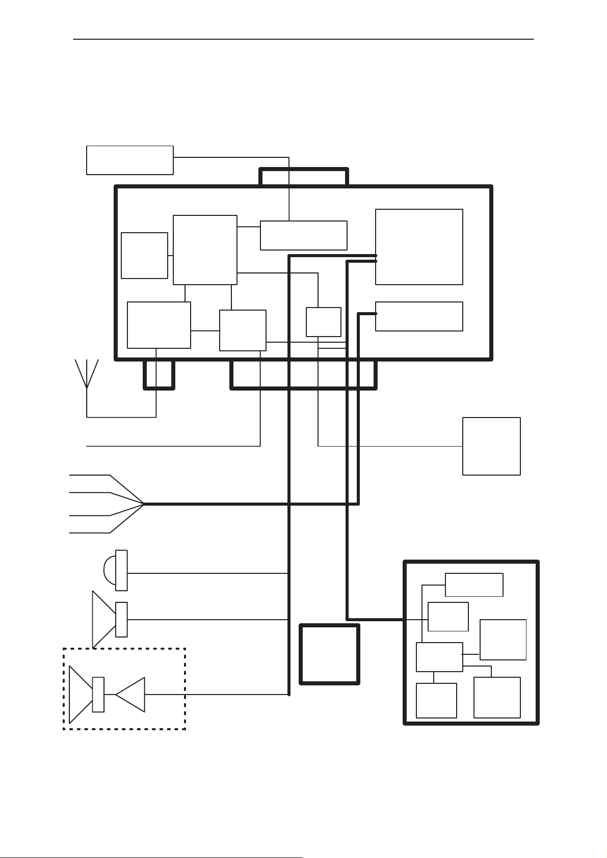
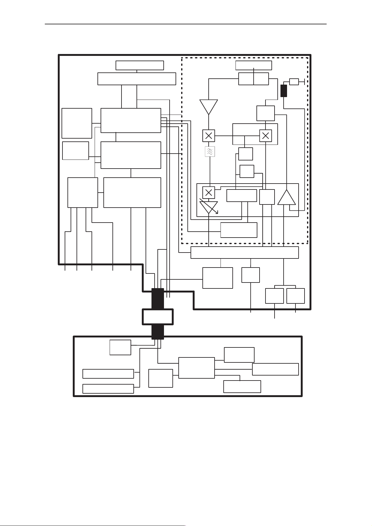
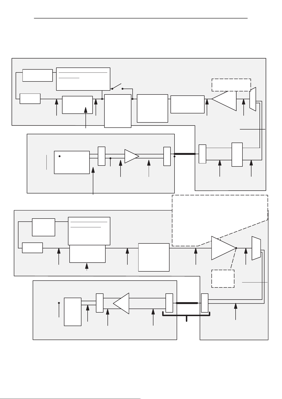
Internal Signals and Connections
LAPTOP
RS 232 Driver
HSIF
Antenna
SIM
Reader
RFPART
DCT 3
Engine
Power
supply
Technical Information
Transceiver
Audio circuits
VDA signals
Battery
Ignition
CRM
AMC
BackLD
HF Microphone
HF Loudspeaker
Carradio
Lineout
Cradle
Power
supply
MCU
Key
board
Car
Data IF
Audio
SIM
Reader
Display
Issue 1 10/99
Figure 3.
Page 15
Page 16
NME–3
Technical Information
PAMS
Technical Documentation
Transceiver
Flash
RAM
EEPROM
SIM
Reader
VDA
signals
DSUB 9
RS 232 Levelshifter
F–Bus
GenIO
MAD2
CCONT
Powersupply
RF–part
LNA
Antenna
Rx Tx
Duplexfilter
CRFU 1A
UHF
VCO
VHF
VCO
Synth
VCTCXO
PA
IQ
Backld
A
M
C
Earpiece amp
Mic–amp
IgnitionCRM
Car bat
Power
supply
M–Bus
COBBA
Handset
audio
interface
Test–
Flash IF
Cradle
Display
MCU
SIM
Reader
Keyboard
Figure 4. CD 949 System overview
HF
preamplifier
Line
Drive
r
HFMicrophone
Lineout
Handset
Illumination
PA
Loudspeaker
Page 16
Issue 1 10/99
Page 17
PAMS
NME–3
Technical Documentation
Row 0..4
Col 0..4
MAD
F–Bus Rx
F–Bus Tx
M–Bus
&
RS232
Level
shifter
Technical Information
System
connector
Data
connector
Flash/Test
equipment
Handset
Figure 5. Digital interface in GM8B
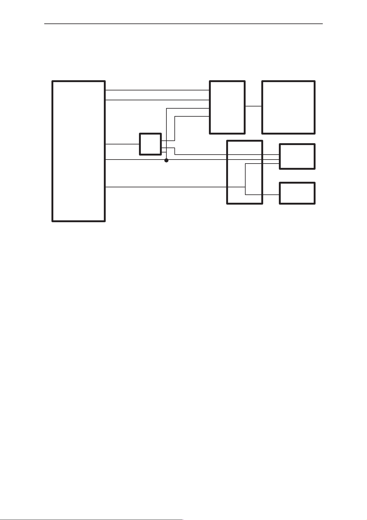
SYS Conn Block Conections
Audio Block Connections
The Cobba has to functions AD/DA converters for the RF–BB interface.
Codecs for the Audio interface. The RF–BB interface is used implemented
in the same way it is implemented in HD940. The Cobba audio interface is
used different to the handys. The Inputs and outputs for HS–use, which
are normally connected directlly to the Microphone and the earpiece are
connected to the Handset via balanced drivers and receivers. The
Handsfree input and output is connected to the analog HFanalog audio
parts on the RU PCB via Balanced lines as well.
Audio Connection to Handset
The audio interface to the HS will not be reused from CD 940. It consists
of balanced audiolines from Cobba to Earpiece and from HS Microphone
to Cobba.
Issue 1 10/99
Page 17
Page 18
NME–3
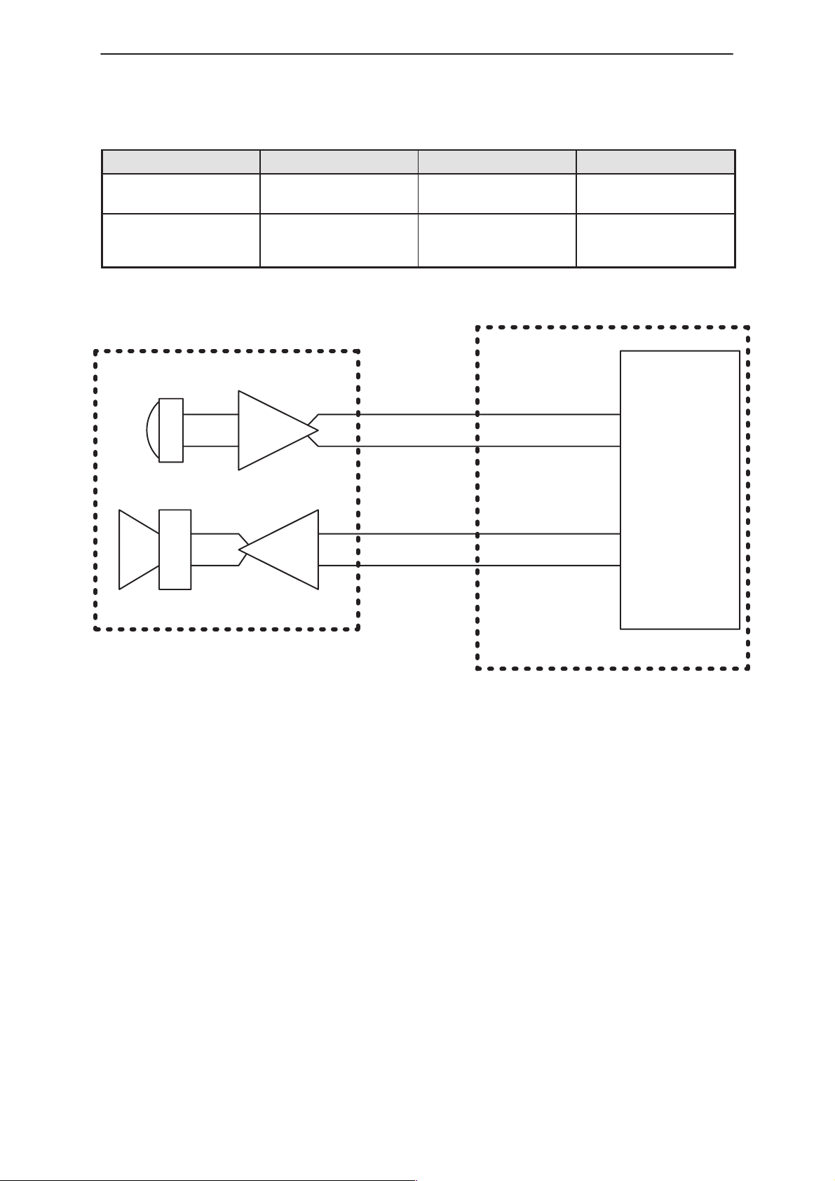
Technical Information
Table 7. Audio levels for HS
Signal name Nominal value Maximum value Notes
Technical Documentation
PAMS
HS EARP/EARN 17,5 mV
HS MICP/MICN 87 mV
RMS
RMS
501 mV
790 mV
RMS
RMS
This is the balanced
signal level at the HS
This is the balanced
signal level at the HS/
RU
Cobba
Handset
Radio Unit
Figure 6. HS audio interface
Page 18
Issue 1 10/99
Page 19
PAMS
NME–3
Technical Documentation
Handsfree Audio Path
DSP
0dB @ 1kHz
Serial Interface
13 bit
parallel
nom: –16dBm0
max: +3,14dBm0
92 mVrms nominal
843 mVrms maximal
Networklevel after
DSP correction:
nom: –16dBm0
max: +3,14dBm0
13 bit ADC
//
6,14 dBm0
@ 0dBV
8kHz
nom: 78mV
max: 707mV
8KHz
2nd
order
300Hz
highpass
filter
0dB @
1KHz
Phone Unit
–11,3dBm0/Pa @ 1kHz from MRP to Network
5th order
3kHz
elyptic
lowpass
filter
0dB @
1kHz
nom: 92mV
max: 843mV
Technical Information
Sending (SLR=8dB)
0–22,5 dB
in 1,5dB steps
anti–aliasing
prefilter
0dB
nom: 78mV
max: 707mV
+ 6 dB
nom: 184mV
max: 1686mV
–20dB
15dB
nom:
18.4mV
max: 168 mV
Cobba
nom: 18,4mV
max: 168mV
Mic1
VDA HF
Microphone
Networklevel after
DSP
0dB @
1kHz
Serial Interface
DSP correction:
nom: –16dBm0
max: +3,14dBm0
13 bit DAC
–7,07 dBVrms
//
@ 0dBm0
13 bit
parallel
nom: –16dBm0
max: +3dBm0
Gain is adjustable from
0 to –30dB in 2dB/4dB steps.
Sorftware is set up to provide
10 volume steps.
– 0dB
– 4dB
– 8dB
–10dB
–12dB
–14dB
–16dB
–20dB
–24dB
–28dB
8kHz
nom: 70,2mV
max: 636mV
8KHz
Phone Unit
Receiving (RLR=2dB)
–33dBPa/–16dBm0 from Network (nominal)
–4dBPa@3.14dBm0 (maximal)
5th order 3kHz
elyptic lowpass
filter
0dB @ 1kHz
LineOut
nom: 70mV
max: 2000mV
nom: 234mV
max: 6700mV
2828mV = 2W at 4W
nom: 70,2mV
max: 636mV
Loudspeaker
–18dB
(nom)
0dB (max)
–9.5 dB
20dB
nom: 23mV
max: 670mV
Gain (see steps
shown left lower)
nom: 14mV
6dB gain
max: 401mV
increase
done
+6dB
nom: 14mV
max: 401mV
nom: 70mV
max: 2000mV
HF
HFCM
Cobba
8dB
8dB
EARP
EARN
Issue 1 10/99
Figure 7. Audio Paths for Hands–Free
Page 19
Page 20
NME–3
Technical Information
Handset Audio Path
PAMS
Technical Documentation
DSP
0dB @ 1kHz
Serial Interface
13 bit
parallel
nom: –16dBm0
max: +3,14dBm0
nom: –4,7dBPa
max: 14,3dBPa
DSP
0dB @
1kHz
Serial Interface
nom: –16dBm0
max: +3dBm0
//
MRP
//
13 bit
parallel
Networklevel after DSP
correction:
nom: –16dBm0
max: +3,14dBm0
13 bit ADC
6,14 dBm0
@ 0dBV
8kHz
nom: 78mV
max: 707mV
8KHz
Mic+Boot
Mic:
–41,7dBV/Pa
@ 1cm @ 1kHz
Vbias
2.2V
nom: 3.28mV
max: 30,0mV
Networklevel after
DSP correction:
nom: –16dBm0
max: +3,14dB
m0
13 bit DAC
–7,07 dBVrms
@ 0dBm0
8kHz
8KHz
2nd order
300Hz
highpass
filter
0dB @
1KHz
–2.8 dB
EMC Filtering
nom: 2.37mV
max: 21.5mV
Handset
Phone Unit
nom: 70,2mV
max: 636mV
31dB
Phone Unit
5th order
3kHz
elyptic
lowpass filter
0dB @ 1kHz
HSMICP
HSMICN
nom: 87mV
max: 790mV
5th order
3kHz
elyptic
lowpass filter
0dB @ 1kHz
Sending (SLR=8dB)
–11,3dBm0/Pa @ 1kHz from MRP to Network
20–42,5 dB
in 1,5dB steps
anti–aliasing
prefilter
0dB
7m cable
0dB
EMC Filtering
– dB
– 6dB
– 8dB
–10dB
–12dB
–14dB
–16dB
–18dB
–20dB
–22dB
–24dB
nom: 78mV
max: 707mV
–18dB (nom)
– 6dB (max)
nom: 70,2mV
max: 636mV
29dB
Fix20dB+
Mic2
VAR9dB
nom: 1.95mV
max: 17.68mV
Cobba
HSMICP
0dB
HSMICN
EMC Filtering
nom: 87mV
max: 790mV
–33 dB
nom: 1.95mV
max: 17.68mV
Gain is adjustable from
0 to –30dB in 2dB steps.
Sorftware is set up to provide 10
volume steps.
nom: 14mV
6dB gain
increase
done
max: 401mV
Cobba
+6dB
EARP/EARN
ERP
Earp
24dB
Pa/V
–12dB
EMC Filtering
@
1kHz
nom: –9,5dBPa
max: 19,5dBPa
nom: 17.7mV
max: 506mV
nom: 70.5mV
max: 2030mV
Receiving (RLR=2dB)
6,5dBPa/0dBm0 from Network to ERP (nominal)
19,5dBPa@3,14dBm0 (maximal)
Figure 8. Audio Path – Hand–Set
Page 20
12.1dB
Handset
HSEARP
HSEARN
EMC Filtering
nom: 17.5mV
max: 501 mV
–__dB
–4 dB
–__dB
EMC Filtering
nom: 28mV
max: 802mV
Issue 1 10/99
EARP
EARN
Page 21

PAMS
NME–3
Technical Documentation
Handsfree Loudspeaker
According to VDA at has to be suitable to drive 4W Loudspeakers with a
maximumpower of 5W. When checking the offical requirements for the
response of the loudspeakerpart, we see that we need to have at 1,5W
Audiopower , if the sensitivity is as specified in CD949 acoustical
components. We are using a bridged Audio Amp. The requirements for
the Loudspeaker are shown below:
Table 8. Loudspeakeroutput
Parameter Value Note
Loadimpedance 3W– 5W
Power at 1% THD 1,5W
minimum drive capacitance 10 nF
Frequency response 300 Hz – 6,8 kHz
Total Powersupply rejection ra-
tio
Technical Information
> 60 dB
Handsfree Microphone
Specification for microphone input
First stage in the CD949 microphone path is an active microphone. This is
needed to get a good signal to noise ration on the long cable between
microphone and CD949 radio unit. The electrical specification for the
microphone (according VDA) could be seen in the table below.
1. 8V Biasvoltage
2. only two Pins
3. 10 kW minimum load
4. at P=74dB,1 khz and 30cm distance it has to deliver 190 mV with a distortion of less then 1%
PP
5. more then 15 dB dynamic range
6. Flat frequency response from 300 Hz to 4 khz +– 1 dB
7. signal to Noise ratio of more then 50 dB at 1% distortion limit
To interface this microphone, the CD949 radio unit has a low noise power
supply The input stage of CD949 has to have an input impedance of >20
kW.
Issue 1 10/99
8. mountable on sunscreen and at chassis of the Car
9. Possibility to drive 7m microphone cable
Page 21
Page 22

NME–3
g
and TX Interstage Am
(VR5)
(32mA)
Receiver (Plussa RX
IFAmp
PLIFIER)
Technical Information
Table 9. Specification for Microphone interface
Parameter Value Notes
Bias voltage 8V +– 10% <10 mV ripple max
Bias source impedance >300 W
Load resistance >10 kW
PAMS
Technical Documentation
AF level 190 mV
pp
15 dB dynamic range
at 1khz
P=74 dB
>1% distortion
The specifications for the line out is that it will be a balanced driver with
the capability of driving high capacitance loads, which are results of long
cables and EMC filtering. The load impedances and voltage levels are
defined and listed in the table below.
Table 10. Line out
Parameter Value Note
Loadimpedance >1k W
Outputlevel max 2000mV RMS
nom 70mV RMS
minimum drive capacitance 1 nF
Frequency response 300 Hz – 6,8kHz only analog Amplifiers
The Interface signals between the Baseband and the RF section of the
CD949 are shown in the following table below. On physical board level the
Baseband supplies voltages from CCONT Asic to seperate RF sub blocks.
The maximum values specified for the digital signals in the table is the
absolute max. value from the RF interface point of view.
Table 11. AC and DC Characteristics of RF baseband signals
Signal
name
VPA
VREF CCONT PLUSSA
VRX1 CCONT
VRX2 CCONT
From To Parameter Mini-
Unreg. car
battery voltage protected
against
overvoltage
(VR2)
RF–PA
PLUSSA
LNA
(25mA),
p
(25mA)
(VRX1)
Typi-
mum
Voltage 10.5 13.0 16.5 V
Current 3150 4500 mA
Voltage 1.478 1.5 1.523 V
Current 100 uA
Source resistance 10 ohm
Voltage 2.7 2.8 2.85 V
,
Current 32 mA
Voltage 2.7 2.8 2.85 V
Current 50 mA
cal
Maxi-
mum
Unit Function
Supply voltage for RF
(controlled with VTX),
plifier (current in TX
slot)
Reference voltage for
PLUSSA and CRFU1a
Supply voltage for RF
section)
Supply voltage for RF
Receiver (LNA, IFAM-
Page 22
Issue 1 10/99
Page 23

PAMS
()
(),
(VR3)
(19mA)
Synthesizer Digital
(),
(V5V)
Charge
Charge Pum s on the
g(
(VR7)
CRFU1a
TX arts on Plussa
NME–3
Technical Documentation
Table 11. AC and DC Characteristics of RF baseband signals (continued)
name
VXO CCONT
(VR1)
VSYN CCONT
VVCO CCONT
(VR4)
VCP CCONT
VCTCXO
(2mA),
Buffer
(5mA)
PLUSSA
UHFVCO
(10mA),
VHFVCO
(5mA),
CRFU1a
(7mA),
buffer
(10mA)
PLUSSA
Pumps
Technical Information
ParameterToFromSignal
Voltage 2.7 2.8 2.85 V
Current 7 mA
Voltage 2.7 2.8 2.85 V
Current 19 mA
Voltage 2.7 2.8 2.85 V
Current 32 mA
Voltage 4.8 5.0 5.2 V
Current 4 mA
Mini-
mum
Typi-
cal
mum
FunctionUnitMaxi-
Supply voltage for RF
VCTCXO and buffer
stage to Plussa if required
Supply voltage for RF
Part (VP1, VP2, VDD)
Supply voltage for RF
VCOs including a buffer and VDDSTBYBIAS
and VDDSTBYLB pins
of the CRFU1a
Supply voltage for RF
p
Plussa ASIC
V8P A VBBDIG Logic cir-
cuits P A
VTX CCONT
VXOPWRMAD CCONT
SYNPWRMAD CCONT
RXPWR MAD CCONT
PLUSSA
Voltage 7.60 8.0 8.40 V
Current 40 60 mA
Voltage 2.7 2.8 2.85 V
Current 72 mA
Logic high ”1” 2.0 2.85 V VR1, VR6 in CCONT
Logic low ”0” 0 0.8 V VR1, VR6 in CCONT
Current 0.1 mA
Timing inaccuracy 10 us
Logic high ”1” 2.0 2.85 V VR3, VR4 in CCONT
Logic low ”0” 0 0.8 V VR3,VR4 in CCONT
Current 0.1 mA
Logic high ”1” 2.0 2.85 V VR2, VR5 in CCONT
Supply voltage for RF
PA logic circuits (controlled with TXP), OpAmp for PA biasing
Supply voltage for RF
p
and CRFU1a
ON
OFF
ON
OFF
ON
TXPWR MAD CCONT
Issue 1 10/99
RF–part
Logic low ”0” 0 0.8 V VR2, VR5 in CCONT
OFF
Current 0.1 mA
Logic high ”1” 2.0 2.85 V VR7 in CCONT ON
Logic low ”0” 0 0.8 V VR7 in CCONT OFF
Current 0.1 mA Switches V8PA ON/
OFF
Page 23
Page 24

NME–3
O
VC(TC)XO
cuits
cuits
Technical Information
Table 11. AC and DC Characteristics of RF baseband signals (continued)
PAMS
Technical Documentation
name
PDATA0 MAD LNA
SENA MAD PLUSSA
SDATA MAD PLUSSA
SCLK MAD PLUSSA
ParameterToFromSignal
Logic high ”1” 2.0 2.85 V Nominal gain in LNA
Logic low ”0” 0 0.8 V Reduced gain in LNA
Current 0.1 mA
Logic high ”1” 2.0 2.85 V
Logic low ”0” 0 0.8 V
Current 50 uA
Load capacitance 10 pF
Logic high ”1” 2.0 2.85 V
Logic low ”0” 0 0.8 V
Load impedance 10 kohm
Load capacitance 10 pF
Data rate frequency 3.25 MHz
Databits S10–S14 10101
Logic high ”1” 2.0 2.85 V
Logic low ”0” 0 0.8 V
Load impedance 10 kohm
Mini-
mum
Typi-
cal
mum
FunctionUnitMaxi-
PLL enable
Synthesizer data
Synthesizer clock
AFC COBBA VCTCXO
RFC VCTCXO MAD
RXIP/
RXIN
PLUSSA COBBA
Load capacitance 10 pF
Data rate frequency 3.25 MHz
Voltage 0.046 2.254 V
Resolution 11 bits
Load resistance
(dynamic)
Load resistance
(static)
Noise voltage 500 uVrms
Settling time 0.5 ms
Frequency 13 MHz
Signal amplitude 0.5 1.0 2.0 Vpp
Load resistance 10 kohm
Load capacitance 10 pF
Output level 50 1344 mVpp
Source impedance tbd. ohm
Load resistance 1 Mohm
Load capacitance tbd. pF
10 kohm
1 Mohm
Automatic frequency
control signal for
VC(TC)X
10...10000Hz
High stability clock signal for the logic cir-
Differential RX 13 MHz
signal to baseband
Page 24
Issue 1 10/99
Page 25

PAMS
f
ulator
NME–3
Technical Documentation
Table 11. AC and DC Characteristics of RF baseband signals (continued)
name
TXIP/
TXIN
COBBA PLUSSA
Technical Information
ParameterToFromSignal
Differential voltage
swing
DC level 0.784 0.8 0.816 V
Differential offset
voltage (corrected)
Diff. offset voltage
temp. dependence
Source impedance 200 ohm
Load resistance 40 kohm
Load capacitance 10 pF
DNL +/–
INL +/–1 LSB
Mini-
mum
1.022 1.1 1.18 Vpp
Typi-
cal
mum
+/–
2.0
+/–
1.0
0.9
mV
mV
LSB
FunctionUnitMaxi-
Differential in–phase
TX baseband signal
or the RF modulator
TXQP/
TXQN
TXP MAD PLUSSA
COBBA PLUSSA
Group delay missmatch
Differential voltage
swing
DC level 0.784 0.8 0.816 V
Differential offset
voltage (corrected)
Diff. offset voltage
temp. dependence
Source impedance 200 ohm
Load resistance 40 kohm
Load capacitance 10 pF
Resolution 8 bits
DNL +/–
INL +/–1 LSB
Group delay mis-
smatch
Logic high ”1” 2.0 2.85 V
Logic low ”0” 0 0.8 V
1.022 1.1 1.18 Vpp
100 ns
+/–
2.0
+/–
1.0
0.9
100 ns
mV
mV
LSB
Differential quadrature
phase TX baseband
signal for the RF modulator
Transmitter power
control enable
Issue 1 10/99
Load Resistance 50 kohm
Load Capacitance 10 pF
Timing inaccuracy 1 us
Page 25
Page 26

NME–3
Technical Information
Table 11. AC and DC Characteristics of RF baseband signals (continued)
PAMS
Technical Documentation
name
TXC COBBA PLUSSA
RXC COBBA PLUSSA
ParameterToFromSignal
Voltage Min 0.12 0.18 V
Voltage Max 2.27 2.33 V
Vout temperature
dependence
Source impedance
active state
Source impedance
power down state
Input resistance 10 kohm
Input capacitance 10 pF
Settling time 10 us
Noise level 500 uVrms 0...200 kHz
Resolution 10 bits
DNL +/–0.9 LSB
INL +/– 4 LSB
Timing inaccuracy 1 us
Voltage Min 0.12 0.18 V
Mini-
mum
Typi-
cal
high Z
mum
10 LSB
200 ohm
FunctionUnitMaxi-
Transmitter power
control
Receiver gain control
LOOP MAD2
(DSP
GENOUT1)
Power
Detector
Voltage Max 2.27 2.33 V
Vout temperature
dependence
Source impedance
active state
Source impedance
power down state
Input resistance 1 Mohm
Input capacitance 10 pF
Settling time 10 us
Noise level 500 uVrms 0...200 kHz
Resolution 10 bits
DNL +/–0.9 LSB
INL +/– 4 LSB
Logic high ”1” 2.0 2.85 V Low impedance mode
Logic low ”0” 0 0.8 V High impedance mode
grounded
10 LSB
200 ohm
(High Power level
range (200mW...8W))
(Low Power level
range (3mW...126mW)
Page 26
Current 0.1 mA
Issue 1 10/99
Page 27

PAMS
NME–3
Technical Documentation
Transceiver (NME–3)
Baseband
This chapter of the document describes the baseband module of the
DCT3 engine used in CD949. The Baseband architecture is basically
similar to DCT2 GSM phones. The DCT3 differs from DCT2 in the
integration level of the baseband. In DCT3 the MCU, the system specific
ASIC and the DSP are integrated in one ASIC called MAD. This chip takes
care of all the signal processing and operation controlling tasks of the
phone.
Technical Information
The baseband architecture supports a power saving mode called ”sleep
mode”. This sleep mode shuts off the VCTCXO, which is used as system
clock for RF and baseband. During the sleep mode the system runs from
a 32khz crystal. The phone is woken up by a timer running from this 32khz
clock supply. The sleeping time is determined by some network
parameters. The sleep mode is entered when MCU and DSP are in stand
by mode and the normal VCTCXO clock has been switched off.
The nominal supply voltage for the baseband part of the engine is 2.8V.
Functional Description
The Baseband functions are controlled by the MAD ASIC, which consists
of a MCU a system ASIC and a DSP. The GSM/PCN specific ASIC is
named MAD2. All the MAD ASICs contains the same core processors and
similiar building blocks, but they differ from each other in system specific
functions, pinout and package types.
MAD2 contains the following blocks:
– ARM RISC processor with both 16 bit instruction set (THUMB mode)
and 32 bit instruction set (ARM mode)
– TI LEAD DSP core with peripherials:
– API (Arm Port Interface Memory) for MCU–DSP communication,
DSP code download, MCU interrupt handling vectors (in DSP RAM) and
DSP booting.
– Serial Port (connetion to PCM)
– Timer
Issue 1 10/99
Page 27
Page 28

NME–3
Technical Information
– DSP memory
– BUSC (Bus Controller for controlling accesses from ARM to API, System
logic and MCU externel Memory, both 8– and 16 bit memories)
– System Logic
– CTSI (Clock, Timing, Sleep and Interrpt control)
RFIClk
RFIWrX
PAMS
Technical Documentation
t
WSHL
RFIAD(3:0)
t
WASU
RFIDA(11:0)
t
WDSU
Figure 9. Write cycle timing.
Table 12. Write Cycle Timing Characteristics
Parameter Symbol Min Max unit
Write strobe active delay time tWSHL 20 tcyc–20 ns
Write strobe inactive delay time tWSLH 20 tcyc–20 ns
Address bus set up time tWASU 30 ns
Address bus hold time tWAHD 30 ns
Data bus set up time tWDSU 30 ns
t
WSLH
t
WAHD
t
WDHD
Data bus hold time tWDHD 30 ns
CCONT for CD949
The heart of the power distrubution is the CCONT. It includes all the
voltage regulators and feeds the power to the whole system. The
baseband digital parts are powered from the VBB regulator which
provides 2.8V baseband supply. The baseband regulator is active always
when the phone is powered on. The VBB baseband regulator feeds MAD
and memories plus COBBA digital parts. There is a separate regulator for
a SIM card. The regulator is selectable between 3V and 5V and controlled
by the SIMPwr line from MAD to CCONT. The COBBA analog parts are
powered from a dedicated 2.8V supply VCOBBA. The CCONT contains a
real time clock function, which is powered from a RTC backup when the
power supply is disconnected.
Page 28
Issue 1 10/99
Page 29

PAMS
NME–3
Technical Documentation
Operating mode Vref RF REG VCOB-
VBB VSIM SIMIF
Technical Information
BA
Power off Off Off Off Off Off Pull
down
Power on On On/Off On On On On/Off
Reset On Off
VR1 On
On On Off Pull
down
Sleep On Off Off On On On/Off
Note: COBBA regulator is off in SLEEP mode. Its output pin may be fed from
in SLEEP mode by setting bit RFReg(5) to ’1’ (default).
V
BB
CCONT includes also five additional 2.8V regulators providing power to
the RF section. These regulators can be controlled either by the direct
control signals from MAD or by the RF regulator control register in
CCONT which MAD can update. Below are listed the MAD control lines
and the regulators they are controlling.
– TxPwr controls VTX regulator (VR5)
– RxPwr controls VRX regulator (VR2)
– SynthPwr controls VSYN_1 and VSYN_2 regulators (VR4 and VR3)
– VCXOPwr controls VXO regulator (VR1)
CCONT also generates a 1.5 V reference voltage VREF to COBBA,
PLUSSA and CRFU. The VREF voltage is also used as a reference to
some of the CCONT A/D converters.
In additon to the above mentioned signals MAD includes also TXP control
signals which go to PLUSSA power control block and to the power
amplifier. The transmitter power control TXC is led from COBBA to
PLUSSA.
Operating mode Vref RF REG VCOB-
VBB VSIM SIMIF
BA
Power off Off Off Off Off Off Pull
down
Power on On On/Off On On On On/Off
Reset On Off
VR1 On
On On Off Pull
down
Sleep On Off Off On On On/Off
Issue 1 10/99
Page 29
Page 30

NME–3
Technical Information
Technical Documentation
Characteristics Condition Min Typ Max Unit
Output current VR1–VR6 Vout@2.8V 100 mA
PAMS
Output current VR7
Vout@2.8V 150 mA
Depends on external BJT
Output current VR7BASE
Vout@2.8V –10 mA
Base current limit
Output current VBB On
Vout@2.8V
Current limit 250mA
Output current VBB
Vout@2.8V
Sleep
Current limit 5mA
Output voltage VR1–VR7 over full tempera-
ture, input voltage
and load range
Output voltage VBB over full tempera-
ture, input voltage
and load range
Line regulation (not
VBB)
Line regulation (not
VBB)
F v 10kHz,
2) VBAT>3.15V
F v 100kHz,
2) VBAT>3.15v
Line regulation VBB F v 100kHz
2)
125
1
mA
mA
2.7 2.8 2.85 V
2.7 2.8 2.85 V
49 dB
40 dB
30 dB
Load regulation T = 25_C 0.6 1 mV/mA
Supply current (each reg-
ulator) VR1...VR7
Supply current VBB ON mode I
Supply current VBB SLEEP mode I
ON mode I
/60
out
+330
/60
out
+
250
/60
out
+
100
I
/10
out
+540
I
/10
out
+
400
I
/10
out
+
150
mA
mA
mA
Page 30
Issue 1 10/99
Page 31

PAMS
NME–3
Technical Documentation
Switching SIM power supply
Technical Information
There is a switched mode supply for the SIM–interface. SIM voltage is
selected via serial IO. The 5V SMR can be switched on independently of
the SIM voltage selection, but can’t be switched off when VSIM voltage
value is set to 5V.
Characteristics Condition Min Typ Max Unit
Output current VR1–VR6 Vout@2.8V 100 mA
Output current VR7
Depends on external BJT
Output current VR7BASE
Base current limit
Output current VBB On
Current limit 250mA
Output current VBB
Sleep
Current limit 5mA
Vout@2.8V 150 mA
Vout@2.8V –10 mA
Vout@2.8V
Vout@2.8V
125
1
mA
mA
Output voltage VR1–VR7 over full tempera-
2.7 2.8 2.85 V
ture, input voltage
and load range
Output voltage VBB over full tempera-
2.7 2.8 2.85 V
ture, input voltage
and load range
Line regulation (not
VBB)
Line regulation (not
VBB)
Line regulation VBB F v 100kHz
F v 10kHz,
2) VBAT>3.15V
F v 100kHz,
2) VBAT>3.15v
49 dB
40 dB
30 dB
2)
Load regulation T = 25_C 0.6 1 mV/mA
Supply current (each reg-
ulator) VR1...VR7
Supply current VBB ON mode I
Supply current VBB SLEEP mode I
ON mode I
/60
out
+330
/60
out
+
250
/60
out
+
100
I
/10
out
+540
I
/10
out
+
400
I
/10
out
+
150
mA
mA
mA
CCONT use in CD949
The CCONT is the Powersupply asic in the DCT3 architecture. The main
difference between the HD940 and the CD949 CCONT application is that
in CD949 all the charging and battery related signals are disabled. The
EAD ADC input is used for backlightdimming. The PowerOnX pulse for
the CCONT is generated by 3 different sources
Issue 1 10/99
Page 31
Page 32

NME–3
Technical Information
1. Ignition gets High
2. The Powerbuttom is pressed
3. The Supplyvoltage comes up from below 3.8V
4. PURX gets low caused by softwarecrash
Handset interface
The handset interface is implemented using the M–Bus. M–Bus is used
for Test puposes as well, but since M–Bus is a multipointbus there is no
problem in using M–Bus for multiple purposes.
For Test and Flash purposes F– and M–Bus are directly connected from
the MAD to the systemconnector. This enables us to use the common Test
and Flash utilities used for HD 941 and HD 943 for CD949 in the same
way.
Multiplexing the Busses
PAMS
Technical Documentation
The M–Bus is a multipoint bus, that could be used for both purposes
(Test/Flash and Handset) without any restrictions. The F–Bus is designed
as a point to point bus, so that it is not possible to connect it to 2 parties
(Data–If and Test IF) directlly. In CD949 it is implemented in a way that
the F–Bus TX from the MAD is going to the Data interface and the Test
interface. The Signals coming from the 2 interfaces are combined by a
AND–gate before they are going to the F–BUS RX. This means that you
could try to use both interfaces at the same time without any risk of
damage to any device, but it is not possible to make data transfer via the
RS232, will using the F–Bus for test or trace purposes. This is no major
drawback, because when you are flashing or aligning the product in the
factory, you are not using the data interface, and the enduser who need s
the Data interface is not touching the test interface at all.
SIM Card in RU
Due to the fact that we are reusing the CD745 mechanical parts we have
also to reuse the CD745 SIM card reader.
Power up/Power down procedure
In the gm8b the CCONT is acting as Reset and Powercontrol Master, as
well as as watchdogtimer. In a normal handportable DCT3 phone the main
powerupprocedure works as following: The user presses the powerbutton,
this signal is delivered to the CCONT via its poweronxpin. If this signal is
valid for more then 50mS the CCONT turns on PURX in order to RESET
the MAD and handover the control to the MAD. When the phone is
switched off or the software crashes the MAD is no longer reseting the
CCONTs watchdogtimer , the watchdogtimer gives an alert, CCONT
switches PURX off and puts the phone into sleepmode.
Page 32
In case of a handy its O.K. when the user has to switch on the phone
again after a softwarecrash, in a carphone (without a handset ??) he won’t
even realise that there is a problem, so this behaviour is not acceptable.
Issue 1 10/99
Page 33

PAMS
NME–3
Technical Documentation
Description of gm8b Powerup/Powerdown behaviour
In a carphone there are 2 sources that wakeup the system in a normal
situation:
1. Ignition is turned on
2. The User presses the Powerbutton
In both situations the phone has to stay in Power On status as long as the
Userpresses the Powerbutton again or Ignition is turned OFF. It should not
be switched off when the software crashed
To gauranty this behaviour, we have added several extra circuits around
CCONT. In gm8b are 4 events that generate a 100mS pulse on poweronx
and switch on CCONT.:
1. Ignition is switched ON
2. Powerbutton is pressed
Technical Information
In order to decide if the PURX is going low because of a Softwarecrash, or
because of a regular Shutdown, there is a Powerdown signal going from
MAD to the Powercontrol unit. When the SW is initiating a Shutdown,
Powerdown is set high, and the Pulse generator is disabled, and no Pulse
is generated on the falling edge of PURX. The following pictures are
ilustrating the Powerup/Down behaviour.
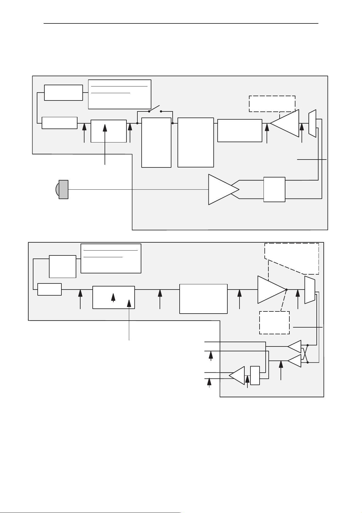
Wakeupevent
(IGNS/Powerbutton)
PowerOnX
3. The Carbatteryvoltage comes up from below 3.8V (Brownout).
4. PURX goes down caused by a software crash
200mS
200us
PURX
Powerdown
Issue 1 10/99
50mS
Figure 10. regular Startup
Page 33
Page 34

NME–3
Technical Information
Wakeupevent
(IGNS/Powerbutton)
PowerOnX
200us
PURX
PAMS
Technical Documentation
200mS
50mS
Powerdown
PURX
PowerOnX
Figure 11. unvalid wakeup (ignored)
50mS
200mS
200us
Powerdown
Page 34
Figure 12. SW crash + Restart
Issue 1 10/99
Page 35

PAMS
NME–3
Technical Documentation
PURX
PowerOnX
Powerdown
Figure 13. regular Shutdown
Description of the Brownout circuit
Technical Information
The CD949 transceiver is permanently connected to the Car battery which
has a nominal level of 13.5 V. Since there are some systems in a car like
ignition or electirical motors, it happens frequently that the voltage drops
below 4V or even down to 0V, for times up to several seconds. Since it is
impossible to buffer the voltage for such a long time we implemented a
strategy called Brownout into GM8B Power control. The Basic idea behind
this strategy is that if the voltage drops, the MAD gets an interrupt, saves
the last state in the EEPROM, and shutsdown. When the Power is back
the Brownout logic indicates to the software that a Power drop has
happened, the software gets the data from the EEPROM, and resets the
Brownout logic.
Issue 1 10/99
Page 35
Page 36

NME–3
Technical Information
VBAT
VBCCONT
VBB
Powercritical
PAMS
Technical Documentation
PowerOnX
Brownoutdet
Brownoutreset
EEPROMACCESS
Figure 14. Brownout procedure total powerdrop
VDA Car Signals
Ignition sense
For GM8B, Ignition sense is an Input. This signal is turned high when the
cars ignition is turned on, and low when the ignition is turned off again.
The system behaviour regarding this signal is so that the phone is turned
on, when Ignition is turned on, and turned off a programmable time after
igntion is turned OFF
Page 36
Issue 1 10/99
Page 37

PAMS
NME–3
Technical Documentation
Table 13. Ignition sense
Parameter max typ min Notes
active voltage Ignition ON 16 V 13,5 V 9 V
inactive voltage Ignition OFF 0,3 V 0 V
Current taken from this signal 1 mA 10mA
Maximum voltage in Fault condi-
tion
Implementation
28 V
80V
The Ignition sense Input is limited to 2.8V via an Resistor/ Z–Diode
combination. The resuting signal is routed to a GENIO of the MAD, it is
also a trigger signal for the wakeup logic.
Car Radio Mute
This signal is an output of CD949. It is an open collector output that is
turned Low when a call is active.
Technical Information
for up to 60s
for 500mS
Table 14. Antenna motor control
Parameter max typ min Notes
High voltage 16 V 9 V No call active
Low voltage 0.3 V call active
External pullup resistor 1 kW
maximum drive current 150 mA
The CRM implementation is reused from PHF–4, but is is not forfilling the
Low–voltage requirement of 0.3V at the moment. But it is no real problem
to make a version that forfills this specification.
Antenna Motor Control
This signal is an output of CD949. It is turned high when the phone ON
and turned LOW when the phone is turned off
Table 15. Antenna motor control
Parameter max typ min Notes
Phone On 16 V 9V
Phone Off 0.3V 0V
drive current 100mA
The Implementation of the AMC is completelly reused from DME–1D
Issue 1 10/99
Page 37
Page 38

NME–3
Technical Information
Backlight Dimming
Technical Documentation
The Backlight dimming is used to synchronise the dimming of all
backlights inside the cars cockpit. The Backlightdimming signal is a PWM
modulated signal that is delivered from the car to the GM8B.
Table 16. Backlight dimming
Parameter max typ min Notes
High voltage 16V 13.5V 9V
pulsewidth 100% 18% for supplyvoltage < 13 V
pulsewidth 100% 13% for supply voltage < 16 V
frequency 120 Hz 60 Hz
PAMS
Rise and fall times dV/dt
dI/dt
The Backlight dimming signal is inverted by an transisitor and then routed
through an single gate inverter, to provide the following Lowpassfilter with
an symetrical Push–Pull driver. The Lowpassfilter has a corner frequency
of 0.1, to provide the ADC of the CCONT with the DC voltage that is
proportional to the Dutycycle of the Backlight dimming signal. The
information about the Duty cycle will be transfered as an M–Bus message
to the Handset in order to dim the LEDs in the Handset.
When an unprogrammed module is powered up the first time the MCU
starts from the boot rom inside the MAD2. The MBUS line is to be kept
low to inform the MCU that the flash prommer is connected and the MCU
should stop after the boot and wait for a download code.
When the flash programming is performed successfully the MCU switches
to flash prom software. If the baseband is powered up for the first time the
MCU will remain in local mode as the factory set has not been executed.
To allow re–programming of working modules the MCU is at startup forced
into local mode by connecting the MBUS to GND.
200
mV/ms
20
mA/mS
Page 38
Issue 1 10/99
Page 39

PAMS
NME–3
Technical Documentation
RF
Item Values
Receive frequency range 935 ... 960 MHz
Transmit frequency range 890 ... 915 MHz
Duplex spacing 45 MHz
Channel spacing 200 kHz
Number of RF channels 124 (+50)
Power class 2 (39 dBm)
Number of power levels 18
Maximum Ratings
Nominal PA voltage: 13.5V
Lower extreme supply PA voltage: 10.5V
Higher extreme supply PA voltage: 16.5V
Technical Information
Table 17. Main RF characteristics
Nominal BB supply voltage is (CCONT) : 2.80V
Lower extreme voltage: 2.70V
Higher extreme voltage: 2.85V
Supply voltage for PA control logic: 8.00V
Lower extreme voltage: 7.60V
Higher extreme voltage: 8.40V
Supply voltage for charge pumps(CCONT) : 5.00V
Lower extreme voltage: 4.8V
Higher extreme voltage: 5.2V
Power Distribution
The following diagram shows the power distribution of the GM8B rf
engine. All major rf modules are supplied with 2.85V from the BB ASIC
CCONT. The specification of the regulators in the CCONT ASIC can be
found in one of the following tables. In addition to this there is a dedicated
8V regulator for the supply of the PA control circuits as well as some buffer
stages. The rf power amplifier itself is directly supplied by the car battery.
Issue 1 10/99
Page 39
Page 40

NME–3
Technical Information
12 V
BATTERY
3,15 A
PA
PAMS
Technical Documentation
VBATT
TXP
V8PA
3
19mA
VR
4
32mA
VCOs
VVCO
VR5VR6VR
0mA
PLUSSA
RX
(VRX)
COBBA
ANAL.
VCOBBA
7
PLUSSA
72mA
VTX
VREF
0,1mA
PLUSSA
CRFU
VREF
V5V
4mA
CHARGE
PUMPsCRFU TX
VCP
30 mA 10 mA
LO Buffer
TX Buffer
PA control
circuits
VR1VR2VR
7mA
VCTCXO
VXO
72mA
CRFU RX
VRX
PLLs
VSYN
Figure 15. Power distribution diagram
Control Signals
Table 18. Control signals and typical current consumptions
VXOENASYNPWRRXPWR TXPWR TXP Typ.
Notes
current
cons.
L L L L L <10 uA Leakage current ( PA )
VBBDIG
VXOENA
SYNPWR
RXPWR
TXPWR
H L L L L 7.0 mA VCTCXO
H H L L L 60 mA VCTCXO, VCOs, PLLs
act.
H H H L L 130 mA RX active
H H L H H 130 mA TX active except PA
H H L H H 3280 mA TX active, full power
All control signals are generated by MAD using 2.8 V logic.
Output Power
Table 19. List of supply voltages
Regulator in CCONT Name of supply Load Current consumption
VR1 VXO VCTCXO
VCTCXO Buffer
VR 2 VRX1 LNA
IF Amplifier
VR 3 VSYN Digital circuits off
PLLs in PLUSSA
2 mA
5 mA
max. 25 mA
max. 25 mA
20 mA
Page 40
Issue 1 10/99
Page 41

PAMS
NME–3
Technical Documentation
Table 19. List of supply voltages (continued)
VR 4 VVCO UHFVCO
VR 5 VRX2 Plussa RX path max. 32 mA
VR 6 VCOBBA COBBA analog circuits BB responsibility
VR 7 VTX PLUSSA and CRFU 1a
V5V VCP Charge pumps in
VREF VREF Reference voltage for
––– V8PA TX buffer
VHFVCO
CRFU 1a
TX path
PLUSSA
CRFU1a and PLUSSA
LO buffer
Bias of detector diode
OPAMPs for PA control
Technical Information
Current consumptionLoadName of supplyRegulator in CCONT
10 mA
5 mA
7 mA
72 mA
4 mA
15 mA
15 mA
10 mA
––– VPA Supply voltage PA max. 4 A
Functional Description
The RF block diagram shows a conventional dual conversion receiver and
the transmitter uses a single upconversion mixer. The architecture
contains two RF ASICs, PLUSSA and CRFU1a.
CRFU1a is a BiCMOS circuit containing the LNA, RX mixer and TX mixer
stages for the handportable GSM phones. However, in order to fulfill the
specifications for the CD949 project a discrete LNA and a discrete RX
mixer were employed.
PLUSSA is also a BiCMOS circuit which contains the IQ modulator for the
transmitter and the receiver stages between the channel filter and
COBBA. It also contains the PLLs for both the VHF and UHF synthesizers.
The Power amplifier is a MMIC ( monolithic microwave integrated circuit )
supplied by Hitachi. It has three amplifier stages including input and
interstage matching.
Using the high integrated engine of DCT3 as much as possible reduces
the component count. With this approach we want to fulfill the high
demands for the reliability demands of the automotive industry.
Issue 1 10/99
Page 41
Page 42

NME–3
Technical Information
PAMS
Technical Documentation
Detector
VPA
Coupler
8Watt PA Module
LNA
935–960MHz
890–915MHz
Int
ers
tag
e
Fil
LNA
25
ter
21, 22 24, 27
int
ers
tag
e
filt
er
VR1
VCP
VREF
V8PA
VPA
VR2
4 mA
100 uA
60 mA
4400 mA
VR3
VR4
VR5
V5V
VR7
VREF
V8PA
BB
Upc
onv
erte
r
7 mA
VXO
82 mA
te
m
p
co
m
p
PLUSSA
TQFP 64
VRX
VSYN
VVCO
(VRX)
VTX
19 mA
32 mA
0 mA
72 mA
Mixer
IF
A
13MHz
M
23
10
9
Mixer
P
8
7
RF
71MHz
Analog RX AGC
Out
58Mhz
:4
In
V
:2
C
ha
rg
eP
116MHz
Out
IN
C
O
Bu
ffe
r
232MHz
1006–1031
VHF Prescaler
PDATA0
VXOENA
SYNPWR
RXPWR
TXPWR
RX
IN
P
RXC
RX
SCLK
IN
SDATA
SENA1
N
AFC
RFC
u
UHF Prescaler
m
IN
p
C
Out
ha
rg
eP
Bias Out
u
m
p
116MHz
buffer
Digita
l TX
AGC
TX Power Control
TXC
Det In
Vo
lta
ge
di
vi
de
r
TXP
TXC
LOOP
TXIP
TXIN
TXQP
TXQN
(Not
used
in
GSM)
Figure 16. Block diagramm of the CD949 GSM RF part
925–960
MHz
880–915
MHz
Page 42
CRFU_1
LO–
buffers
1st IF 71 MHz
LO–
buffers
996–
1031
MHz
TX IF 116 MHz
UHF
PLL
f/2
2nd LO
58 MHz
f
f
PLUSSA
f
f/2f/2
VHF
PLL
Figure 17. RF frequency plan
2nd IF 13 MHz
232
MHz
13 MHz
VCTCXO
Issue 1 10/99
Page 43

PAMS
NME–3
Technical Documentation
Receiver
The transceiver uses a dual conversion linear receiver. The received
signal from the antenna is fed via the duplex filter to a discrete LNA ( low
noise amplifier ) which uses a BFP420 transistor. The LNA can be
switched between two gain settings in order to increase the dynamic
range of the receiver. Switching of the LNA is controlled using the PDATA0
line from MAD using a discrete transistor network. The gain step in the
LNA is activated when the RF input level at the antenna is less than –50
dBm.
Following the LNA, the signal is fed to the SAW interstage bandpass filter.
This filter in combination with the helical duplex filter defines the spurious
signal blocking for the receiver, in particular rejection of the image for
mixing to the first RX IF frequency at 71 MHz.
The first mixer is a double balanced (quad diode hybrid) type. This is
necessary in order to fulfill the strict blocking requirements, in particular
the half IF rejection is critical. To provide the required gain an IF amplifier
follows the mixer. Since the passive mixer requires a high LO signal level,
additional local signal buffering is provided by a discrete buffer. The mixer
uses upper sideband injection for generating the IF signal. The LO signal
is generated with the UHF synthesizer.
Technical Information
The first IF signal is then channel filtered by a bandpass SAW filter with a
bandwidth of ±100 KHz. It also provides attenuation to the image
frequency for mixing to the second IF frequency (13MHz).
This filter also stops signals and mixing products at frequencies outside of
the channel bandwidth from saturating proceeding amplifier stages,
therefore reducing receiver sensitivity.
The next stage in the receiver chain is the AGC amplifier which is
integrated into the PLUSSA ASIC. The control voltage for the AGC is
generated by the DAC in the COBBA ASIC and provides a gain control
range of 57 dB. The second mixer stage is also integrated into PLUSSA.
The LO signal for the mixer stage is generated by dividing the VHF
synthesizer frequency by a factor of four to produce 58 MHz. The resulting
2nd IF signal is at 13 MHz.
The 2nd IF filter is a ceramic bandpass filter located outside of PLUSSA. It
is centered at 13 MHz with a bandwidth of ±100 KHz. The purpose of this
filter is to attenuate signals at the adjacent channel frequencies except for
the neighboring channels at ± 200 KHz which are filtered digitally by the
DSP. The dynamic range of the DACs within COBBA is wide enough to
cope with the effects of fading, particularly when the signal strength of the
interferer is high.
After the 13 MHz filter there is a buffer stage in PLUSSA which converts
the signal from single ended to differential to drive the DACs. The buffer
has a voltage gain of 36 dB and the buffer gain setting in COBBA is 0 dB
or 9.5 dB if required.
Issue 1 10/99
Page 43
Page 44

NME–3
Technical Information
Transmitter
The transmitter chain contains an IQ–modulator, an upconversion mixer, a
power amplifier and a power control loop.
The I and Q signals are generated by the DACs in COBBA in the BB
section, post filtered (RC–network) and fed into the PLUSSA IQ
modulator. The modulated IF signal from this modulator is centered at
116MHz (this is the VHF synthesizer frequency divided by two (232MHz)).
Following the modulator, the signal is fed to a cascaded variable gain
amplifier. It’s gain is set to a fixed value of +4dB by a data word coming
from the MCU in MAD. (This cascaded amplifier is used in other digital
systems as well with stepped amplification values. PLUSSA is a core IC
created to fulfill different standards and frequency concepts.) This first TX
IF signal is then bandpass filtered and fed into the CRFU_1a. The TX part
of this ASIC contains a double balanced Gilbert cell (which is an image
rejection upconversion mixer), a buffer and two phase shifters for the LO
signal. The CRFU_1a’s output is single ended, therefore no external balun
is necessary. The LO signal is generated by the UHF–synthesizer, fed into
the phase shifters and then into the Gilbert cell.
PAMS
Technical Documentation
The signal at the final TX frequency is then fed to a TX interstage filter, a
buffer, a PA, a directional coupler, a duplex filter and and the antenna
connector. The TX interstage filter is a bandpass type (dielectric or SAW
filter) which attenuates the spurious signals of the upconverter and
reduces the wideband noise of the signal. The buffer stage is used to
provide the PA with sufficient input power. The final amplification is done
by a Hitachi MosFet PA module. This module is internally matched to 50
ohm and is able to provide 20W of output power using an input level of
approximately +3dBm. The power control range of this device is
approximately 100dB.
The directional coupler is designed to measure the PA output power. The
output power is detected by a detector diode and is used for the power
control loop. A duplex filter provides sufficient TX/RX isolation and filters
the harmonics generated by the PA.
Frequency Synthesizers
Both PLLs use the same reference signal generated by a13 MHz
VCTCXO module ( voltage controlled crystal oscillator ). Temperature
compensation is controlled by AFC ( automatic frequency control ). The
VCTCXO frequency is adjusted using the signal received from the base
station. AFC is generated by baseband with a 11 bit conventional DAC in
COBBA.
Page 44
PLUSSA contains the UHF PLL with prescaler, N, A and R dividers,
phase detector and charge pumps. The prescaler is a dual modulus 64/65
(P/P+1) type and the charge pump supply current to the external loop
filter. All PLL dividers are programmed via the 3–wire bus (i.e. SDATA,
SCLK and SENA1).
The output signal of the prescaler is fed to N and A divider which
produces one of the inputs to the phase detector.
Issue 1 10/99
Page 45

PAMS
NME–3
Technical Documentation
The phase detector compares this signal with the reference signal divided
by the reference divider from the VCTCXO. The error signal generated by
the phase detector drives the charge pumps. The current pulses
generated by the charge pumps are integrated by the loop filter to
produce a control voltage for the UHF VCO. The settling time of the
synthesizer is defined by the loop filter component values. The channel
spacing is equal to the comparison frequency which is 200 KHz.
: R
f
ref
f_out /
M
PHASE
DET.
M = A(P+1) + (N–A)P=
= NP+A
CHARGE
PUMP
Kd
freq.
reference
AFC–controlled VCTCXO
LP
VCO
Kvco
: M
Technical Information
f_out
Figure 18. Phase locked loop , PLL
The VHF PLL is also located in PLUSSA. There is a 16/17 ( P/P+1 ) dual
modulus prescaler, N and A dividers, reference divider, phase detector
and charge pumps. The VHF signal is generated by a discrete VCO
circuit. The VHF PLL works in the same way as the UHF PLL. The VHF
PLL operates at a fixed frequency (232 MHz) regardless of the traffic
channel frequencies. A frequency divider is used after the VHF VCO in
order to reduce phase noise.
Receiver Characteristics
RF Characteristics, Receiver
Table 20. Receiver characteristics
Item Values
Type Linear, FDMA/TDMA
IF frequencies 1st 71 MHz, 2nd 13 MHz
LO frequencies 1st LO 1006 ... 1031 MHz, 2nd LO 58 MHz
Typical 3 dB bandwidth (reference noise band-
width)
+/– 90kHz
Sensitivity min. – 104 dBm , S/N >8 dB
Total typical receiver voltage gain ( from antenna
to RX ADC )
Receiver output level ( RF level –104 dBm ) 50 mVpp ( typical balanced signal level of 13
MHz IF in RF BB interface = input level to RX
Typical AGC dynamic range 50 dB
Accurate AGC control range 57 dB
Issue 1 10/99
88 dB
ADCs )
Page 45
Page 46

NME–3
Technical Information
Table 20. Receiver characteristics (continued)
Typical AGC step in LNA approx. 45 dB
Usable input dynamic range –104 ... –10 dBm
RSSI dynamic range –112 ... –48 dBm
PAMS
Technical Documentation
ValuesItem
AGC relative accuracy on channel ( accurate
range )
Compensated gain variation in receiving band +/– 1.0 dB
+/– 0.8 dB
Receiver Module Specification
Duplex filter
Table 21. Duplex filter specification
Parameter Transmit section Receive section unit
Center frequency,
ftx,frx
BW ( bandwidth ) at
passband
Maximum insertion
loss at BW
Minimum insertion loss 0.3 – dB
Ripple at BW, peak to
peak
Terminating imped-
ance
ftx : 902.5 frx : 947.5 MHz
+/– 12.5 +/– 12.5 MHz
1.5 2.8 dB
1.0 1.0 dB
50 50 ohms
min. input/output
matching Mag(S11)
and Mag(S
Minimum attenuations
Permissible input power
Temperature Range –35 ... 85 –35 ... 85 deg Cel
22
)
Freq.range Att. Freq.range Att.
640 ... 820 20 0...800 35 MHz/dB
925 ... 940 30 890...915 15 MHz/dB
940 ... 960 30 980...1050 15 MHz/dB
960 ... 976 10 1067...1102 35 MHz/dB
1574 ... 1577 25 1102...2000 25 MHz/dB
1760 ... 1830 30 2000...3500 30 MHz/dB
2640 ... 2745 30 MHz/dB
3520 ... 3660 30 MHz/dB
–11 –11 dB
4 AVG W
Page 46
Issue 1 10/99
Page 47

PAMS
NME–3
Technical Documentation
Pre–amplifier Specifications
Technical Information
The LNA is a discrete solution using a BFP420 as active component.
Table 22. LNA requirements
Parameter Min. Typ. Max. Unit/Notes
Frequency band 935 – 960 MHz
Supply voltage 2.7 2.8 2.855 V
Current consumption 25 mA
Insertion gain Mag(S21) 19 20 21 dB
Noise figure 1.8 2.0 dB,PDATA0=H
IIP3 –2 dBm, PDATA0=H
Input 1 dB compression point –12 dBm, PDA TA0=H
Reverse isolation Mag(S12) 25 dB
Input matching Mag(S11) –7 dB
Output matching Mag(S22) –10 dB
Gain reduction 35 40 dB,room temp.
Step accuracy –2 +2 dB,over temp.range
Noise figure, when PDATA=0 25 dB
RX Interstage Filter
Table 23. RX interstage filter requirements
Parameter Min. Typ. Max. Unit
Passband 935 – 960 MHz
Insertion loss 4.0 dB
Ripple in passband 1.0 dB
Attenuation DC...890 MHz 35 dB
Attenuation 890...915 MHz 15 dB
Attenuation 980...1030 MHz 15 dB
Attenuation 1067...1 102 MHz 35 dB
Attenuation 1102...1500 MHz 30 dB
Terminating impedance 50 ohm
Input matching Mag(S11) –9.5 –9.5 dB
Maximum drive level +10 dBm
Issue 1 10/99
Page 47
Page 48

NME–3
Technical Information
Diode Mixer Specification
The 1st mixer will be a passive quad diode hybrid as it was used in
CD745.
PAMS
Technical Documentation
Table 24. Mixer requirements
Parameter Min. Typ./
Nom.
RX frequency range 935 960 MHz
LO frequency range 1006 1031 MHz
LO drive level +6 dBm
IF frequency 71 MHz
Conversion gain –7 dB
NF, SSB 7 dB
IIP3 +13 dBm
1 dB Compression Point +3 dBm
IF/2 spurious rejection 67 dBm, *
LO power level in RF–port –25 dBm
Input matching Mag(S11) –9.5 dB
Impedance 50 ohm
IF Amplifier Specification
Table 25. Electrical characteristics
Max. Unit/Notes
Parameter min. typ. max. unit
Operating temperature range –30 +85 deg.C
Supply Voltage 2.7 2.8 2.85
Current Consumption 22 25 mA
Center frequency , fo 71 MHz
Insertion Gain 21 22 23 dB
Noise figure 2 3 dB
IIP3 –1 dBm
1dB Input Compression Point –11 dBm
In– / Output matching 50 ohm
IF Filter Specification
Table 26. Electrical characteristics
Parameter min. typ. max. unit
Operating temperature range –30 +85 deg.C
Center frequency , fo 71 MHz
Maximum ins. loss at 1dBBW 11 dB
Group delay ripple at 1dBBW 1.3 us pp
Page 48
Issue 1 10/99
Page 49

PAMS
NME–3
Technical Documentation
Table 26. (continued) Electrical characteristics
Bandwidth relative to 71 MHz
1 dB bandwidth
3 dB bandwidth
5 dB bandwidth
22 dB bandwidth
30 dB bandwidth
40 dB bandwidth
Spurious rejection, fo +/– 26 MHz 65 dB, *
Terminating impedance ( balanced )
resistance
capacitance ( parallel )
CRFRT RX Part Specification
+/– 90
+/–120
2k||10p kohm||pF
Technical Information
unitmax.typ.min.Parameter
kHz
+/– 230
+/– 350
+/– 550
+/– 700
In CD949 the IF backend is build around the DCT3 ASIC Plussa. Also an
additional 13 MHz filter is used. The specification of this filter is also
added into this chapter.
Table 27. AGC and 2nd mixer in PLUSSA, requirements
Parameter Min. Typ. Max. Unit/Notes
Supply voltage 2.7 2.8 2.85 V
Current consumption (VRX) 32 mA
Input frequency range 45 120 MHz
2nd IF frequency range 0.4 17 MHz
Total noise figure, SSB,
max. gain
Total noise figure, SSB,
min. gain
Max. voltage gain 40 dB
Min. voltage gain –17 dB
Control voltage for min. gain 0.5 V
Control voltage for max. gain 1.4 V
Output 1 dB compression
point @ max. gain
Input 1 dB compression point
@ min. gain
IF input impedance (bal-
anced)
800 mVpp
80 mVpp
2.4/tbd 3.8/2 5.6/tbd kohm/pF
15 dB
65 dB
2nd mixer output impedance
( single output )
Issue 1 10/99
100 ohm
Page 49
Page 50

NME–3
Technical Information
Table 28. 2nd IF–filter connected to PLUSSA
Parameter min. typ. max. unit
Center frequency, fo 13 MHz
Technical Documentation
PAMS
1 dB bandwidth, 1 dBBW
( relative to 13 MHz )
Insertion loss 8.0 dB
Amplitude ripple at 1 dBBW 1.0 dB
Group delay ripple at 1 dB
BW, peak to peak
Attenuations, relative to
13 MHz
fo +/– 400 kHz
fo +/– 600 kHz
fo +/– 800 kHz
+/– 90 kHz
1.5 us
25
35
35
Transmitter Characteristics
RF Characteristics, Transmitter
Table 29. Transmitter characteristics
Item Values
Type Upconversion, nonlinear, FDMA/TDMA
Intermediate frequency ( phase modulated ) 116 MHz
LO frequency range 1006 ... 1031 MHz
dB
Max. Output power 8 W peak
Gain control range min. 34 dB
Maximum phase error ( RMS/peak ) max 5 deg./20 deg. peak
Table 30. Output power requirements
Parameter Min. Typ. Max. Unit / Notes
Max. output power 39.0 dBm
Max. output power tolerance
(power level 2)
Output power tolerance /
power levels 3...15
Output power tolerance /
power levels 16...19
Output power control step
size
0.5 2.0 3.5 dB
+/– 2.0
+/– 2.5
+/– 3.0
+/– 4.0
+/– 5.0
+/– 6.0
dB, normal cond.
dB, extreme cond.
dB, normal cond.
dB, extreme cond.
dB, normal cond.
dB, extreme cond.
Page 50
Issue 1 10/99
Page 51

PAMS
NME–3
Technical Documentation
Technical Information
Sub Block Description/Tables
Electrical Specifications, CRFRT TX Section
In the CD949 rf module the modulator is integrated into the DCT3 ASIC
Plussa.
Table 31. Requirements for IQ–modulator
Parameter Min. Typ. Max. Unit
Supply voltage 2.7 2.8 2.85 V
Current consumption (VTX) 28 tbd. mA
Modulator Inputs (I/Q) Minimum Typical /
Nominal
Input bias current (balanced) 100 nA
Input common mode voltage 0.8 V
Input level (balanced) 1.2 Vpp
Input frequency range 0 300 kHz
Input resistance (balanced) 200 ohms
Maximum Unit / Notes
Input capacitance (balanced) 4 pF
IQ–input phase balance
total, temperature included
IQ–input phase balance
temperature effect
IQ–input amplitude balance
total, temperature included
IQ–input amplitude balance
temperature effect
Modulator Output Minimum Typical /
Output frequency 85 400 MHz
Available linear RF power
into 100 ohm balanced load
Available saturated RF power
into 100 ohm balanced load
(max. gain in AGC)
Noise level in output –145 dBm/Hz avg.
Total gain 4 dB
–4 4 deg.
–2 2 deg.
–0.5 0.5 dB
–0.2 0.2 dB
Maximum Unit / Notes
Nominal
–9 –7 dBm
–5 –3 dBm
The modulated TX signal is centered at 116MHz. Following the modulator
this signal is fed through an discrete filter to suppress any high frequency
harmonics.
Table 32. 116 MHz LC IF–filter, requirements
Parameter Min. Typ. Max. Unit
Center frequency 116 MHz
Insertion loss @ 116 MHz 3.0 dB
Relative attenuation @ +/– 10
MHz offset
5 dB
Issue 1 10/99
Page 51
Page 52

NME–3
Technical Information
Table 32. 116 MHz LC IF–filter, requirements (continued)
PAMS
Technical Documentation
UnitMax.Typ.Min.Parameter
Relative attenuation @ +/– 20
MHz offset
Relative attenuation @ 232
MHz
Relative attenuation @ 348
MHz
Relative attenuation @
464–1000 MHz
Input impedance, balanced 100 ohm
Output impedance, balanced 200 ohm
Mixer Specification
Table 33. Requirements for the upconversion mixer in CRFU_1a
Parameter Min. Typ. Max. Unit
Supply voltage 2.7 2.8 2.85 V
Supply current 50 mA
Input frequency 116 MHz
Input level –8 –5 dBm
8 dB
15 dB
20 dB
25 dB
Output frequency range 890 915 MHz
Output level +3 +5 dBm
NF,SSB 20 dB
LO–signal level in output –29 dBc
Unwanted sideband level –15 dBc
fLO+/–2xIF spurious level –40 dBc
7x116 MHz spurious level –40 dBc
8x116 MHz spurious level –55 dBc
Input impedance (balanced) 200//tb
d.
Output matching Mag(S22)
( with matching network )
–9.5 dB
ohm//pF
Page 52
Issue 1 10/99
Page 53

PAMS
NME–3
Technical Documentation
TX Filter Specifications
Table 34. Specification TX interstage filter
Parameter Min. Typ. Max. Unit
Passband 890 – 915 MHz
Insertion loss 3.5 dB
Ripple in passband 1.5 dB
Attenuation DC...813 MHz 30 dB
Attenuation 925...935 MHz 4.5* dB
Attenuation 935...960 MHz 5** dB
Attenuation 1006...1031 MHz 40 dB
Attenuation 1122...1147 MHz 30 dB
Attenuation 1780...1830 MHz 10 dB
Attenuation 2670...2745 MHz 10 dB
Terminating impedance 50 ohm
Input/Output matching Mag(S11)
Mag(S22)
–8 dB
Technical Information
Maximum drive level +10 dBm
Power Amplifier
Table 35. Specification MosFet power amplifier Tamb = +25 deg. C, 50 ohms
Parameter Symbol Test condition Min Typ Max Unit
Operating freq. range 890 915 MHz
Supply voltage 10.5 12.5 16.5 V
Current consumption,
extreme conditions
Current consumption,
nominal conditions
Input power Pin 3 13 dBm
Output power 1 Pout 1 Pin= 3 dBm, VDD=12.5 V,
Output power 2 Pout 2 Pin= 3 dBm, VDD=10.3 V,
Power control range Vapc= 2 ... 7 V 100 dB
Isolation Pin= 3 dBm, VDD=12.5 V,
Pout=41.5dBm, VDD=10.5V 4.5 A
peak
Pout=41.5dBm, VDD=13V 3.15 3.65 A
peak
42.3 43.6 dBm
Vapc=7 V , Tc=+25 deg.C
39.5 40.8 dBm
Vapc=7 V , Tc=+80 deg.C
–60 –40 dBm
Vapc=0.5 V , Tc=+25 deg.C
Carrier switching time tr, tf VDD=12.5 V, Pin=3 dBm
Pout= 13W
Total efficiency
Control current Iapc
Harmonics, 2nd –50 –40 dBc
Harmonics, 3rd –55 –45 dBc
Pin= 3 dBm , Pout= +41.1
dBm, VDD=12.5 V
30 35 %
Issue 1 10/99
1.5 2 us
0.9 mA
peak
Page 53
Page 54

NME–3
Technical Information
Table 35. Specification MosFet power amplifier (continued) Tamb = +25 deg. C, 50 ohms
Input matching
Mag(S11)
Technical Documentation
–9.5 –6.0 dB
PAMS
UnitMaxTypMinTest conditionSymbolParameter
Operating case temperature
storage temperature –40 +110 _C
APC voltage Vapc 0 8 V
Duty cycle Pout=41.5dBm, VDD=10.5V
Pin= 3 dBm, Tc=+25 deg.C
Stability
Load mismatch stress
Power Control Circuit
Table 36. Directional coupler characteristics
Parameter Min. Typ. Max. Unit/Notes
Frequency range 890 915 MHz
Insertion loss 0.4 dB
Coupling factor 20 dB
Directivity 30 dB
Impedance level of the
main line
Matching main line Mag(S11)
and Mag(S22)
Pin= 3 dBm, VDD=12.5 V,
Load VSWR 20:1, all phases
50 ohm
–20 dB
–30 +110 _C
50 %
no parasitic oscillation
Impedance level of the
coupled line
Table 37. Specification of the Power Detector
Parameter Test condition Min Typ Max Unit
Freq. Range 890 915 MHz
InputPower Power Level 19 – 2 –13 21 dBm
Linear range
Dynamic range
Output Voltage Low Power Mode tbd
Output Voltage High Power Mode tbd
Supply Voltage 7.6 8 8.4 V
Supply current
Temperature Drift tbd mV
100 ohm
tbd
(1.65)
(1.65)
(2.0)
tbd
(3.6)
V
V
Page 54
Issue 1 10/99
Page 55

PAMS
NME–3
Technical Documentation
Table 38. Dual range power control loop characteristics
Parameter High power loop Low power loop
Power level 2 ... 10 11 ... 19
DET voltage 200mV ... 1250mV 250mV ... 1580mV
LOOP amplification factor 0.5 5
Bias voltage for PA 2V ... 7V 1.7V ... 2V
Table 39. Dual range power control loop characteristics
Parameter High power loop Low power loop
Power level 2 ... 10 11 ... 19
DET voltage 200mV ... 1250mV 250mV ... 1580mV
LOOP amplification factor 0.5 5
Bias voltage for PA 2V ... 7V 1.7V ... 2V
Technical Information
Table 40. Specification of the TXC Offset shifter
Parameter Test condition Min Typ Max Unit
Supply Voltage 7.6 8V 8.4 V
Min output voltage tbd 1.2 V
Max output voltage Low Power Mode tbd 2.3 V
Max output voltage High Power Mode tbd 4.2 7 V
Temperature drift from –20 C to +80 C, de-
pends on 8V temp. drift
Table 41. Specification of the Error amplifier
Parameter Test condition Min Typ Max Unit
Supply voltage 7.6 8.0 8.4 V
Min output voltage MC 33074 @ 5V – 0.1 0.3 V
Max output voltage MC 33074 @ 5V 3.7 4.0 – V
Gain tbd (15) 1
fc tbd (35) kHz
tbd mV
Temperature drift from –20 C to +80 C tbd (0) mV
Issue 1 10/99
Page 55
Page 56

NME–3
Technical Information
Technical Documentation
Synthesizer
VCTCXO
Table 42. Electrical specifications
Parameter Min. Typ. Max Unit/.Notes
Supply voltage, Vcc 2.70 2.80 2.90 V
Current consumption, Icc 1.5 mA
Operating temperature range –30 +85 deg. C
Nominal frequency 13 MHz
PAMS
Output voltage swing
( swing of 13 MHz component, selective measurement from the spectrum )
Load, resistance
capacitance
Frequency tolerance @+25 deg. C – 1.0 + 1.0 ppm
Frequency tolerance after reflow
( @ +25 deg. C )
Frequency stability vs. temperature
( ref. @+25 , –30....+85 deg. C )
Frequency stability vs. supply voltage ( 2.8 V +/– 100 mV )
Frequency stability vs. load change
( 2 kohm//10 pF +/– 10 % )
Aging – 1.0 + 1.0 ppm/year
Nominal control voltage, Vc 1.3 V
Voltage control range 0.3 2.3 V
Voltage control characteristics
( see note 1. )
800 mVpp
2
10
– 2.0 + 2.0 ppm
– 5.0 + 5.0 ppm
– 0.1 + 0.1 ppm
– 0.3 + 0.3 ppm
+/– 14 +/– 20 ppm/V when
kohm
pF
0.3 V<Vc<2.3 V
Vc input resistance 1 Mohm
Frequency adjustment +/–
3.0
Harmonics ( with 2 kohm//10 pF ) – 5 dBc
Start up time
output level within 90%
output frequency limits +/–0.5ppm
from the final value
Phase noise @ 1 kHz offset –130 dBc/Hz
4.5
Page 56
ppm with inter–
nal trimmer
ms
Issue 1 10/99
Page 57

PAMS
NME–3
Technical Documentation
VHF VCO + Filter
Table 43. VHF VCO requirements
Parameter Min. Typ. Max. Unit/Notes
Supply voltage range 2.7 2.8 2.9 V
Current consumption 7 mA
Control voltage 0.5 4.0 V
Operation frequency 232 MHz
Output level –13 –10 dBm ( output after
Harmonics –30 dBc, ( filtered )
Phase noise,
fo +/– 600 kHz
fo +/– 1600 kHz
fo +/– 3000 kHz
Control voltage sensitivity 8.0 16.0 MHz/V
Pushing figure +/– 2 MHz/V
–123
–133
–143
Technical Information
low pass filter )
dBc/Hz
Frequency stability +/– 3 MHz ( over temper-
ature range –30...+85 C deg.)
Spurious content –70 dBc
UHF PPLL
Table 44. UHF–synthesizer, requirements
Parameter Min. Typ. Max. Unit/Notes
Start up settling time 3.0 ms
Settling time +/– 25 MHz 500 800 us, ( into +/– 20 Hz
from final frequency )
Phase error 3.7 deg./rms
Sidebands
+/– 200 kHz
+/– 400 kHz
+/– 600...+/–1400 kHz
+/–1.4... +/– 3.0 MHz
> +/– 3.0 MHz
UHF VCO
Table 45. UHF VCO module, Electrical specifications, Zo=50 ohm
–40
–60
–66
–76
–86
dBc
Parameter Conditions Rating Unit/
Notes
Supply voltage, Vcc 2.8 +/– 0.1 V
Supply current, Icc Vcc = 2.8 V,
Vc= 2.25 V
Control voltage, Vc Vcc = 2.8 V 0.8... 3.7 V
Oscillation frequency Vcc = 2.8 V
Vc = 0.8 V
Vc = 3.7 V
Issue 1 10/99
< 10 mA
< 1006
> 1031
Page 57
MHz
MHz
Page 58

NME–3
Technical Information
Table 45. (continued) UHF VCO module, Electrical specifications, Zo=50 ohm
PAMS
Technical Documentation
RatingConditionsParameter
Tuning voltage in center frequency f = 1013.5 MHz 2.25 +/– 0.25 V
Tuning voltage sensitivity in operating
frequency range on each spot freq.
Output power level Vcc=2.7 V
Output impedance and VSWR f=1006...1031
Phase noise, fo +/– 25 kHz
fo +/– 600 kHz
fo +/– 1600 kHz
fo +/– 3000 kHz
Pulling figure VSWR=2, any
Pushing figure Vcc=2.8 +/– 0.1
Frequency stability over temperature
range
Harmonics –10 max. dBc
Vcc = 2.8 V
f=1006...1031
MHz
f=1006...1031
MHz
MHz
Vcc=2.8 V
f=1006...1031
MHz
phase
V
Ta=–30 ... +85
deg. C
16+/– 2 MHz/V
–6.0 min. dBm
50 ohms,VSWR
<2
–100
–120
–130
–140
+/– 1.0 MHz
+/– 2.0 MHz/V
+/– 3.0 MHz
Unit/
Notes
dBc/Hz
max.
max.
max.
max.
Spurious Vcc=2.8 V,
Vc=0...6 V
Input capacitance in Vc–pin Vc= 0 V 100 max. pF
UHF VCO Buffer
Table 46. Buffer for RX downconverter
Parameter Min. Typ. Max. Unit/Notes
Supply voltage 7.8 8.0 8.2 V
Supply current 15 mA
Frequency range 1006 1031 MHz
Input power –6 dBm
Output power 6 dBm
1 dB input compression –7 dBm
IIP3 +3 dBm
Harmonics –45 dBc
–70 max. dBc
Page 58
The RX LO buffer is a discrete realization and amplifies the UHF LO signal
to the level required by the RX mixer.
Issue 1 10/99
Page 59

PAMS
NME–3
Technical Documentation
Table 47. UHF local signal input in CRFU_1a
Parameter Min. Typ. Max. Unit/Notes
Input frequency range 990 1040 MHz
Input level 200 700 mVpp
Input resistance 100 ohm
Input capacitance 1.5 pF
PLL Circuit
Table 48. UHF PLL block in PLUSSA, requirements
Parameter Min. Typ. Max. Unit/notes
Input frequency range 650 1700 MHz
Input signal level (f<1.5 GHz) 200 mVpp
Input resistance 600 700 Ohm
Input capacitance 1.8 3 pF
Technical Information
Supply current 10 12 mA
Reference input frequency 13 MHz
Reference input impedance 10||1 kΩ ||pF
Phase comparison frequency 1 MHz
Charge pump output
current 1
current 2
Sink to source current matching error of the charge pump
Charge pump current error +/– 10 %
Charge pump current temper-
ature variation
Charge pump leakage current 5 nA
Phase detector phase noise
level
0.5
2.0
mA
+/– 5 %
+/– 10 %
–163 dBc/Hz
Antenna
In CD949 the responsibility for the antenna is at the customer. The CD949
project responsiblility ends at the RF connector (MINI–UHF type). The
impedance at this point is 50 Ohm. The antenna connection itself is
designed to withstand 16.5V DC. This is achieved by DC decoupling by a
simple capacitor in series to the rf input.
Antenna Specification
There is no antenna specification for the CD949 antenna. Any standard
active or passive GSM antenna should work together with CD949.
Issue 1 10/99
Page 59
Page 60

NME–3
Technical Information
Handset (RTE–2HJ)
Power up/Power down procedure HS
PAMS
Technical Documentation
This task is divided up between hard– and software to protect accidential
power down of SIM. As long, ”+5V” is below 4.63V, Reset is active (active
LOW, Net: _RESOUT), and min. 20msec after 4.63V was reached. After
_RESET is high, software has to wait in a loop until Net: ”SUPPLYOK”
goes high. This is at the point, where the Voltage supplied via Cable is
over 7 Volt. After this happens, HS–Microcontroller can start the normal
program (with SIM–start). If Voltage supplied via Cable goes below 6.2
Volts, the microcontroller is interupted via ”SUPPLOWIRQ” (active low),
then it must be monitored. If it is low for a certain time, the system has to
be shut down. This shut down should terminate in the wait loop from the
beginning (until SUPPLYOK).
The HS will be connected with a 10 pol RJ45 connector to the cabletree
which is going to the RU.
On the HS PCB there is a 1*10 pol male right angle connector typ SMK
CGP4710–0101 to connect the curly cord to the HS.
D.C. Characteristics
Supply Voltage
To supply the HS different voltages are needed, they are generated from
the 8V supply of the RU. In the HS there are regulators for generating
stabilized 5V and 3V. The following figure shows the power distribution
inside the HS.
Page 60
Issue 1 10/99
Page 61

PAMS
NME–3
Technical Documentation
8V
Power Supply
8V
5V
3V
Technical Information
BLD
MCU
Memory
Audio
Keyboard
SIM
Reset strategy is divided up between hard– and software to protect
accidential power down of SIM. As long, ”+5V” is below 4.63V, Reset is
active (active LOW, Net: _RESOUT), and min. 20msec after 4.63V was
reached. After _RESET is high, software has to wait in a loop until Net:
”SUPPLYOK” goes high. This is at the point, where the Voltage supplied
via Cable is over 7,0 Volt. After this happens, HS–Microcontroller can start
the normal program (with SIM–start).
If Voltage supplied via Cable goes below 6.0 Volts, the microcontroller is
interupted via ”SUPPLOWIRQ” (active low), then it must be monitored. If it
is low for a certain time, the system has to be shut down. This shut down
should terminate in the wait loop from the beginning (until SUPPLYOK).
Current Consumption
The handset current consumption dependents on three different parts:
1. digital part
LCD
Figure 19. Power distribution diagram
If only the digital part is active (no call active and BLD is switched offf) the
current consumption is around 40 mA. When BLD is switched on with a
duty cycle of 100% the current consumption is increased to approximately
90 mA. Depending on the BLD duty cycle the current consumption is
varying between 40 mA and 90 mA. If a call is active the current
consumtion can increase up to 100 mA when BLD duty cycle is 100%
Issue 1 10/99
2. backlight diming
3. audio
Page 61
Page 62

NME–3
Technical Information
External Signals and Connections
The handset is connected via curly cord to the system cable and then to
the RU. The curly cord uses an 10 pol western plug which will be
connected to the system cable.
HS Module Connector
Table 49. Handset connector
PAMS
Technical Documentation
Pin Line Symbol Minimum Typical /
Nominal
1 N.C. not connected / HS
2 MBUS 0
2.0
9600
3 +8V 7,2 8,0 8,8
4 GND ground from RU
5 HSEARP 17,5 501 mV / earpiece + to
6 HSEARN 17,5 501 mV / earpiece – to
7 PWR_ON
3.6
8 HSMICP 87 790 mV / microphone +
Maximum Unit / Notes
side =GND
0.8
2.8
5
5
100
0.7
3.8
V / low voltage
V / high voltage
µs / risetime
µs / falltime
baud/ transmission
rate
V / supply voltage
mA / supply current
earpiece –
earpiece +
V / low voltage
V / high voltage
to microphone –
9 HSMICN 87 790 mV / microphone –
to microphone +
10 N.C. not connected / HS
side =GND
Pins 1 and 10 are connected to ground in HS for EMC protection
purposes and not connected in RU/ SCM–5.
Functional Description
Power On Key
Power ON/OFF key is connected to the RU via a seperate line. If the DC
level,delivered from the RU, is switched to ground the CCONT in the RU
detect this as power up of the system and switches on RU and HS.
Keypad Switch Matrix
Keyboard is held in SIMPLEX style. Keys are arranged in 4*4 matrix
structure and activities will generate an interrupt. The 4 horizontal rows
are routed to an input port of the MCU and the 4 vertical columns are
routed to an output port of the MCU. After reception of the keyboard
interrupt the SW can determine exactly which key was pressed.
Page 62
Issue 1 10/99
Page 63

PAMS
NME–3
Technical Documentation
LCD Module
As display a passive, full dot matrix (48*84) Liquid Crystal Display module
in foil compensated super twisted nematic technology with integrated
driver from Phillips will be used. Size of the display is 39.5*34*3.5 mm.
The LCD display is working with 3V instead of 5V for the MCU and
therefore a level–shifter is needed between MCU and LCD display. Data
to be displayed will be transfered via a serial communication interface
from the MCU to the LCD display.
Back Light
The Back Light Dimming circuit is used to illuminate the keyboard and
LCD–Display depending from the backlight dimming signal of the car
(Kl.58g). For the HS only yellow green LEDs are used. Inside the RU a
MBUS message is generated and sent to the HS. The MCU of the HS will
then generate two PWM signals to control the back light dimming circuit.
Two PWM signals are generated to have the chance to illuminate
keyboard and LCD–Display in different ways if necessary. The LEDs are
driven by two constant current sources.
Technical Information
Mic/Speaker
As microphone an electret condenser microphone from Matsushita typ
WM–66EC110 will be used. The diameter of the microphone is 6mm.
The microphone signal is bandwidth limited and amplified and routed as
balanced signal to the RU. The needed reference voltage for biasing of
the OPs will be generated by an OP voltage follower out of the 5V supply
voltage. Also this 2.5V voltage is used for biasing of the microphone and
the microphone amplifier.
The balanced earpiece signal from the RU is bandwidth limited and
amplified and then routed thru the earpiece.
A Phillips earpiece typ WD 00918/32U will be used. The diameter is 23
mm.
HOOK Detection
For detection if the HS is inside or outside the cradle a hall detector is
used. The cradle contains there a permanent magnet, so if the HS is
inside the cradle the switch of the hall detector is closed and hook line is
connected to GND. The Hook line then goes to an interrupt input of the
MCU.
MBUS
The bidirectional MBUS between RU and HS is working at 2.8V. Inside the
HS the bidirectional MBUS is split into TX and RX direction and then fed to
one of the serial communication interfaces of the MCU. The split circuit
makes also the level shift from 2.8V to 5V which is needed by the MCU.
The prefered bit rate will be 9600 bit/s but can be speeded up to 19.2
kbit/s if needed by the SW to refresh the LCD display in a sufficient time.
(not needed at the moment, due to successful compression work of the
SW group)
Issue 1 10/99
Page 63
Page 64

NME–3
Technical Information
Memory
The HS has no external FLASH or MASK ROM memory on board so the
ROM is limited to the 128k*8 of the MCU. External RAM (32k*8) is
connected to the MCU.
PAMS
Technical Documentation
Page 64
Issue 1 10/99
Page 65

PAMS
NME–3
Technical Documentation
Cradle (CRD–8))
System Description
The cradle can be used for left and right hand cars and will fit physically
into the cars of MB, Audi and Ford. It will be used together with the Minna
Handset and with the Dude Handset, both handsets having the same
mechanical interface. The Minna HS has an emergency button; the Dude
HS has no emergency button.
Technical Information
Otherwise the HS’s are equal from the mechanical point of view. The
cradle offers the following functionality:
–Locking/release mechanism
–Switch between Hands–free and private mode supported through a
magnet
There is no PCB inside the Cradle and no illumination of the push buttons.
Cradle Concept
The mechanical concept of the cradle is based on the DCT3 cradles and
uses a similar locking/release mechanism. The DCT3 cradle uses one
spring for the whole locking/release mechanism making assembly easier.
The cradle is designed so that the user has easy access to the
locking/release mechanism when used either on dashboard or armrest
mounting.
Issue 1 10/99
Page 65
Page 66

NME–3
Technical Information
Technical Documentation
No. Acc. Characteristics Specification
1 Main Dimensions 94 mm (L) x 71mm (W) x 34mm (H)
2 Weight 60g
3 Materials Housing: PC/ABS
Push Buttons: POM
Slider: PA + GF
4 PCB No PCB
5 Shielding No Shielding
6 Mounting Dashboard & Armrest
7 Mounting Plate CRD–8 Mounting plate or
Swivel Mounting Plate
8 Fixation Screwed
9 Screw Pattern 35mm x 38mm
17,5mm (2 screws)
24,5mm (2 screws)
9 HS Release Button 2
10 Button Illumination No
11 Hook Detection Permanent magnet
12 IP Class IP5K0 with Handset in a mounted
position
IP 30 the cradle
13 Colour Nokia warm black
14 Surface Structure According VDI3400 Ref. 30
15 Temperature Range –40°C…+85°C
16 Mechanical Requirements CD940 Specification.
17 General Mechanical Re-
quirements
NMP SPR 3&4
Car industry req.
PAMS
Page 66
Issue 1 10/99
 Loading...