

Page 1

Nokia Customer Care
6088 (RM-218)
Mobile Terminal
RF Description and
Troubleshooting
Issue 1 10/2006 Company Confidential © 2006 Nokia Corporation
Page 2

6088 (RM-218)
Nokia Customer Care RF Description and Troubleshooting
Contents Page
Component Layout ................................................................................................... 3
Tx Troubleshooting................................................................................................... 5
Tx system block diagram ...................................................................................5
Tx introduction ...................................................................................................6
Main TX component...........................................................................................6
FTM setup for TX troubleshooting......................................................................7
TX DC Test Points..............................................................................................8
Tx RF Test Points...............................................................................................9
Tx DC Test Points ............................................................................................10
Tx path troubleshooting ................................................................................... 11
Rx Troubleshooting ................................................................................................ 12
Rx system block diagram.................................................................................12
Rx introduction.................................................................................................13
Main RX component ........................................................................................13
FTM setup for RX troubleshooting ...................................................................13
Cell Receiver Check from RF to IQ..................................................................14
Receiver DC Test Points..................................................................................16
Receiver RF Test Points ..................................................................................17
Rx path troubleshooting...................................................................................18
Issue 1 10/2006 © 2006 Nokia Corporation Company Confidential Page 2
Page 3
6088 (RM-218)
g
Nokia Customer Care RF Description and Troubleshooting
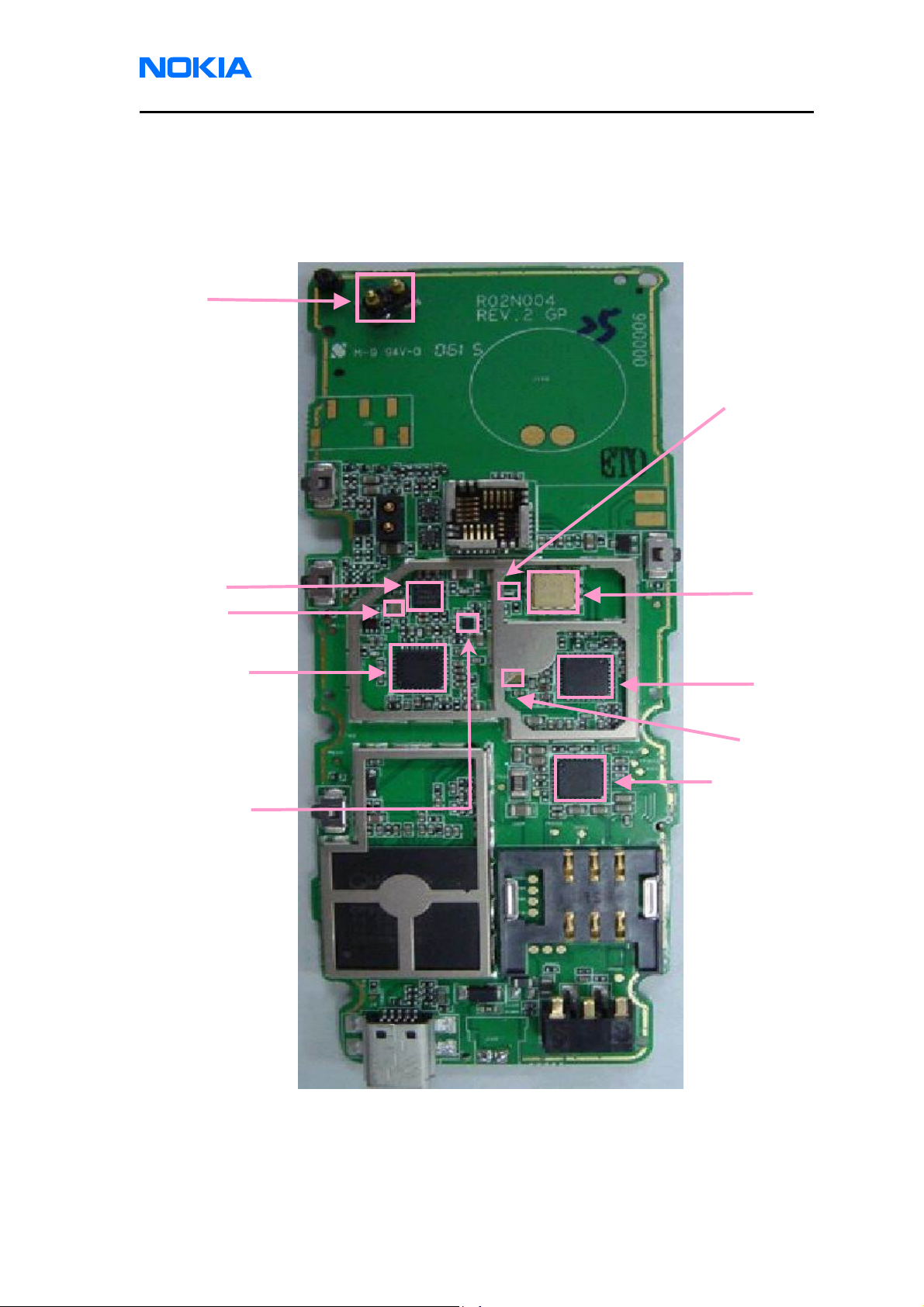
Component Layout
Figure 1 shows the main components of the 6088 mobile terminal.
RFAntenna
Direction Coupler
Power Amplifier
Tx Saw filter
RF Transmitter
Power Detector
Cell Duplexer
RF Receiver
Rx Saw filter
Power Mana
ement IC
Issue 1 10/2006 © 2006 Nokia Corporation Company Confidential Page 3
Page 4
6088 (RM-218)
y
Nokia Customer Care RF Description and Troubleshooting
RF Connector
132.768KHz
stal
Cr
19.2MHz TCXO
Issue 1 10/2006 © 2006 Nokia Corporation Company Confidential Page 4
Figure 1: Component layout
Page 5
6088 (RM-218)
Nokia Customer Care RF Description and Troubleshooting
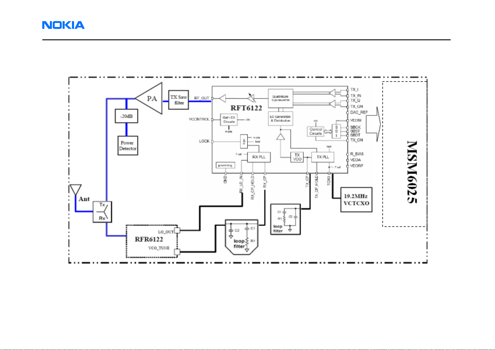
Tx Troubleshooting
Tx system block diagram
Figure 2: Tx system block diagram
Issue 1 10/2006 © 2006 Nokia Corporation Company Confidential Page 5
Page 6
6088 (RM-218)
Nokia Customer Care RF Description and Troubleshooting
Tx introduction
The RFT6122 (Figure 2) provides the Zero-IF transmit signal path for Cellular-CDMA transmission. For this chipset, Cellular-CDMA refers to
band classes 0 and 3 as defined by the cdma2000 standard, with mobile station transmitters operating between 824 and 925 MHz. The
transmit signal path includes baseband amplifiers, quadrature upconversion, gain control RF amplification, and an output driver amplifier.
The driver amplifier output is routed to the final stages of the transmit chain – power amplifier, isolator, duplexer, and antenna.
Main TX component
Power Amplifier
TX Saw filter
Direction coupler
Cell Duplexer
TX IC
Figure 3: Tx components
Issue 1 10/2006 © 2006 Nokia Corporation Company Confide
Power detector
ntial Page 6
Page 7

6088 (RM-218)
Nokia Customer Care RF Description and Troubleshooting
FTM setup for TX troubleshooting
Put PWB on the module jig. Use the following steps to configure FTM for RF
troubleshooting.
1. Select “FTM mode” in Module Jig
2. Connect RF connector to a spectrum by using CA-89RS RF Test Cable
3. Connect 6088 mobile terminal to a PC via Module Jig, and connect power
supply to Module Jig
4. Open RF Tools software in 6088 CCS Level 3 service software
5. The FTM dialog box appears
6. Set COM port to appropriate one in “Select COM port”
7. Set “Connect Phone”
8. Set “Set FTM”
9. Set “Set Band” to “CDMA800”.
10. Set “Set Channel “ to Channel “384”
11. Set “Set Pa Range R1” to “on”
12. Set “Set TX waveform” to “CDMA”
13. Set “Set TX on/off” to “on”
14. Set “Set TX AGC” to “100”
Figure 4: FTM dialog box
Issue 1 02/2006 © 2006 Nokia Corporation Company Confidential Page 7
Page 8

6088 (RM-218)
Nokia Customer Care RF Description and Troubleshooting
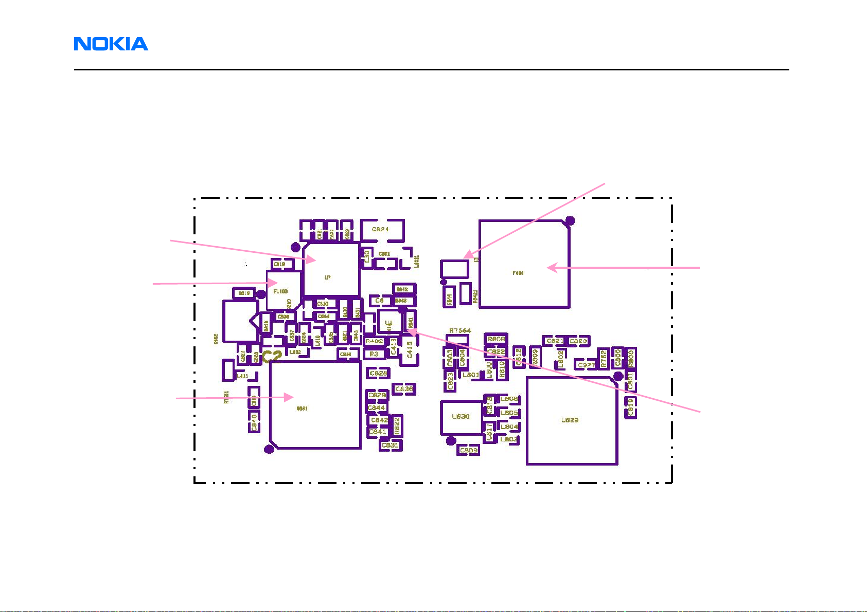
TX DC Test Points
6
1
3
2
4
5
U631pin8
8
Figure 5: Tx DC test point
Table 1: Tx DC Test Points
Test Point Description Value
1 PA_ON 2.86V for PA turning on, 0 V for turning off
2 PA_R1 1.97V for high gain mode,1.38V for low gain mode
3 LOCK_DET 2.95V for Lock, 0 V for unlock
4 TX_AGC
5 Tx IQ in 0.84 V With oscilloscope: 500 mV p-p
6 DAC_REF 1.56V
7 VREG_MSMP 2.96V
8 VREG_RFTX 2.64V
Issue 1 10/2006 © 2006 Nokia Corporation Company Confidential Page 8
1.86V for 5dBm, 2.12V for 15dBm, 2.38V for
25dBm.
7
Page 9

6088 (RM-218)
Nokia Customer Care RF Description and Troubleshooting
Tx RF Test Points
4
2
3
1
5
Figure 6: Tx RF Test Points
Table 2 shows the test points shown in Figure 6.
Test Point Description Value
1 RFT6122 output 3dBm
2 PA input 1dBm
3 PA output 27dBm
4 RF connector 24.5dBm
5 UHF LO 0dBm at 1763.04MHz
Table 2: Tx RF Test Points
Issue 1 10/2006 © 2006 Nokia Corporation Company Confidential Page 9
Page 10

6088 (RM-218)
1
Nokia Customer Care RF Description and Troubleshooting
Tx DC Test Points
7
8
5
6
4
Figure 7: Bottom side Tx DC test points
Table 3 shows the Tx DC test points shown in Figure 7.
1
3
2
Test
Point
1 VREG_MSMP,C861 2.96V >11kΩ to ground U632,U631,U629,U1
2 VPH_PWR,C854
3 VREG_MSMC,C860
4 VREG_MSMA,C858
5 VEXT_DC,R840
6 VREG_TCXO,C857
7 VREG_RFRX,R855
8 VREG_RFTX,C856
Description Value RF Supply Lines Resistance to Ground
3.2~4.2V >550kΩ to ground U632,U7
1.91V >45kΩ to ground U632,U625
2.62V >120kΩ to ground U632,U625
3.2~5.7V ~9.3kΩ to ground Q400
2.82V >450kΩ to ground U632
2.66V >350kΩ to ground U632,U631,U629
2.64V >450kΩ to ground U632,U631,U629
Table 3: Tx DC Test Points and RF Supply Line Resistance to Ground
*Note: Always measure resistance with the phone powered off
Issue 1 10/2006 © 2006 Nokia Corporation Company Confidential Page 10
Page 11

6088 (RM-218)
Y
j
Y
r
j
Y
Y
Nokia Customer Care RF Description and Troubleshooting
Tx path troubleshooting
Tx path
Faults
Measure DC test
points at Table 1. Is
it OK?
NO
Check PM6610, MSM6025 Reheat solder joints of PM6610
YES
Measure Tx RF test
points 5
at Table 2. Is it OK
YES
NO
Rehear solder
oints of C836
Measure Tx RF test
NO
points 1
Change RFT6122
at Table 2. Is it OK
ES
Measure Tx RF test
NO
points 2
Reheat solder joints of C837, FL600, C619, U7
at Table 2. Is it OK
ES
Measure Tx RF test
points 3
Reheat solde
NO
oints of U7
at Table 2. Is it OK
ES
Measure Tx RF test
points 4
at Table 2. Is it OK
ES
If RF Antenna feed point pad
obstructed, clean the pad. Connect
System Simulator to MS antenna. Is it
OK
Reheat solder joints of F601, S601
NO
Note:
• MSM6025 is underfilled and cannot be replaced.
• Memory IC is underfilled and cannot be replaced.
• The shield case can not be reused after removal.
• After using the heatgun, replace the domesheet.
NO
NO
Change U7
Check Antenna Module
NO
Issue 1 10/2006 © 2006 Nokia Corporation Company Confidential Page 11
Page 12

6088 (RM-218)
Nokia Customer Care RF Description and Troubleshooting
Rx Troubleshooting
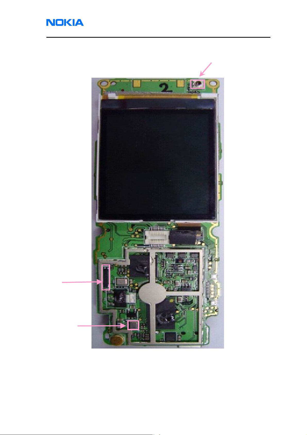
Rx system block diagram
Figure 8: Rx DC troubleshooting test points
Issue 1 10/2006 Company Confidential © 2006 Nokia Corporation Page 12
Page 13

6088 (RM-218)
r
Nokia Customer Care RF Description and Troubleshooting
Rx introduction
The RFR6122 IC (Figure 8) provides the Zero-IF receiver signal path for Cellular-CDMA reception. For this chipset, Cellular-CDMA refers
to band classes 0 and 3 as defined by the cdma2000 standard, with mobile station receivers operating between 832 and 894 MHz. The Rx
signal path includes the LNA, quadrature downconversion, and baseband functions.
The Cellular-CDMA received signal is routed from the antenna to the RFR6122 IC via the duplexer. The analog baseband outputs
interface with one of Qualcomm’s Mobile Station MSM6025 devices that also provide status and control signaling. Integrated RX LO
circuits, ideally supplemented by the RFT6122 transmitter IC, provide frequency plan flexibility and further reduce PCB parts count.
Main RX component
RX Saw filte
RX IC
Issue 1 10/2006 Company Confidential © 2006 Nokia Corporation Page 13
Page 14

6088 (RM-218)
Nokia Customer Care RF Description and Troubleshooting
FTM setup for RX troubleshooting
Put PWB on the module jig. Use the following steps to configure FTM for RF
troubleshooting.
1. Connect RF test connector to a spectrum.
2. Set SW1 to “FTM mode” in Module Jig.
3. Connect the mobile terminal to a PC via the Module Jig, and connect a
power supply.
4. Open CCS Service Software and run RF Tools function.
5. The FTM dialog box appears.
6. “Select COM port” to appropriate one.
7. Set “Connect Phone”.
8. Set “Set FTM “.
9. Set “RF Mode” to “CDMA800”.
10. Set “Set Channel “to Channel “384”.
11. Set “Set LNA Range” to whatever needed.
Figure 9: FTM dialog box
Issue 1 10/2006 © 2006 Nokia Corporation Company Confidential Page 13
Page 15

6088 (RM-218)
Nokia Customer Care RF Description and Troubleshooting
Cell Receiver Check from RF to IQ
Use the following values to check the CDMA Cell Rx functionality from RF to IQ
output.
1. Start FTM in Local Mode with only the Rx path turned on and set
LNA_GAIN_STATE=0.
2. Inject a –75 dBm CW signal of 881.82 MHz (i.e. 300 kHz offset from 881.52 MHz
or 10 channels away).
3. Measure a 300 kHz tuning on the analyzer. You should see a typical -48 dBm IQ
tuning for CDMA Cell.
Figure 10: Receiver IQ level on CDMA Cell band
Issue 1 10/2006 © 2006 Nokia Corporation Company Confidential Page 14
Page 16

6088 (RM-218)
Nokia Customer Care RF Description and Troubleshooting
Figure 11 shows the Cell spectrum with an inject tone at -75 dBm, as well as the IQ
output test points. Note that DC is present on the IQ output test points. All test points
should be approximately equal.
RX _QP
RX _QN
RX _ IN
RX _ IP
Figure 11: Cell spectrum (left) and IQ output test points (right)
Issue 1 10/2006 © 2006 Nokia Corporation Company Confidential Page 15
Page 17

6088 (RM-218)
Nokia Customer Care RF Description and Troubleshooting
Receiver DC Test Points
1
3
2
Figure 12: Rx DC troubleshooting test points
Table 4 includes the descriptions and values for Rx DC troubleshooting test points
shown in Figure 12.
Test Point Description Value
1 VREG_MSMP ,R800 2.96V
2 VREG_RFRX,R7563 2.58V
3 LNA BIAS,L800 2.58V
Table 4: Rx DC Test Points
Issue 1 10/2006 © 2006 Nokia Corporation Company Confidential Page 16
Page 18

6088 (RM-218)
Nokia Customer Care RF Description and Troubleshooting
Receiver RF Test Points
For the test points in Figure 13, an external signal source of –25 dBm was injected to
the RF input. Set LNA GAIN STATE = 3 .The signal was then traced throughout the
receiver chains. An CMU200 call box is recommended. (Open non-signaling mode,
press the SG soft button, and then select CW.) Inject a continuous wave (CW) for
Cell (881.52MHz) at a fixed –25 dBm power level. Measurements were taken with
the RF Probe. Signal levels are approximate, and the accuracy may be +/- 2 dB or
more depending on the probe position and grounding.
2
3
Figure 13: Receiver RF troubleshooting test points
Table 5 includes the descriptions and values for Rx RF troubleshooting test points shown
in Figure 13.
1
Test Point Description Value
1 LNA IN -27dBm
2 RX SAW INPUT -47dBm
3 RX SAW OUTPUT -50dBm
Table 5: Rx RF Test Points
Issue 1 10/2006 © 2006 Nokia Corporation Company Confidential Page 17
Page 19

6088 (RM-218)
Y
Y
Nokia Customer Care RF Description and Troubleshooting
Rx path troubleshooting
Rx path
Faults
Measure DC test
points at Table 4. Is
it OK?
YES
NO
Check PM6610
NO
Reheat solder joints
of PM6610
Measure Rx RF test
points 1
at Table 5. Is it OK
Reheat solder joints
NO
of C820, L802
YES
Measure Rx RF test
points 2
at Table 5. Is it OK
ES
Measure Rx RF test
points 3
NO
NO
Reheat solder joints
of L801, C823 and
RFR6122
Reheat solder joints
of U630
NO
Change RFR6122
at Table 5. Is it OK
ES
Connect System Simulator to
Check Antenna Module
NO
MS antenna.
Note:
• MSM6025 is underfilled and cannot be replaced.
• Memory IC is underfilled and cannot be replaced.
• The Shielding Case Assy cannot be reused after removal.
• After using the heatgun, the domesheet needs to be replaced.
Issue 1 10/2006 © 2006 Nokia Corporation Company Confidential Page 18
 Loading...