Nokia 6085 RM-198 Schematic

Introduction
IMPORTANT:
This document is intended for use by authorized NOKIA service centers only.
“Service Schematics” was created with focus on customer care.
The purpose of this document is to provide further technical repair information for
NOKIA mobile phones on Level 3/4 service activities.
It contains additional information such as e.g. “Component finder”.
The “Signal overview” page gives a good and fast overview about the most
important signals and voltages on board.
Saving process time and improving the repair quality is the aim of this document.
It is to be used additionally to the service manual and other training
or service information such as Service Bulletins.
Service Schematics
RM-198
A NEW FEATURE FOR ON-LINE USE
We have now linked those measurement points which are related to the ocsillograms
shown on the signal overview page. As example: clicking on the measurement point
guides you to the matching oscillogram on the signal overview page. The next click onto
the now shown signal guides you to the related measurement point on the module. Finally,
a third click, now onto the measurement point on the module, takes you back to the
starting point inside the schematics.
Do you have further improvement ideas or would like to give us feedback?
Please send an email to: training.sace@nokia.com
1
1
1
All measurements were made using following equipment:
Nokia repair SW : Phoenix version 2006.34.2.156
Oscilloscope : Fluke PM 3380A/B
Spectrum Analyzer : Advantest R3162 with an analog probe
RF-Generator / GSM Tester : Rhode & Schwarz CMU 200
Multimeter : Fluke 73 Series II
While every endeavour has been made to ensure the accuracy of this document, some
errors may exist. If the reader finds any errors, NOKIA shall be notified in writing.
Please send E-Mail to: training.sace@nokia.com
Table of Content
Front page
System connector
Retu, Tahvo, LED driver
RAPGSM, Memories, FM radio, BT
User interface
Flip PWB
RF part
Signal overview
Component finder
Copyright © NOKIA
This material, including documentation and any related computer programs is protected
by copyright, controlled by NOKIA. All rights are reserved. Copying, including reproducing,
modifying, storing, adapting or translating any or all of this material requires the prior
written consent of NOKIA. This material also contains companyconfidential information,
which may not be disclosed to others without the prior written consent of NOKIA.
1
2
3
4
5
6
7
8
9
Customer Care / Training & Vendor Development/ Content Creation Team
Confidential - Copyright © 2006 NOKIA Only for training and service purposes
Version: 2.0 05.10.20
0
6085/ RM-198
6
Board version: 1VZ_12
Fr
ont page
Page 1 (9)

Tahvo
Retu
FM radio
CHARGER
XAUDIO(7:0)
FMANT(1:0)
0
1
2
3
4
5
6
7
R2004
10R
HOOKDET
MICB2
MIC2P
XEARL
XEARLC
XEARR
XEARRC
C2007
10n
GND
0
R2005
Charger plug
L2000
220R/100MHz
V2000
L2001
R2006
KA
GND
1
23
B2GND
C2016
470n
GND
C2000
27p
J2002
R2000
220R
C2002
2u2
GND
C2003
33n
C2004
33n
R2002
C2008
10n
R2003
10R
10R
J2003
J2004
C2009
C2010
10n
10n
GND
GND
J2005
J2006
GND
10R
GND
to UEME
R2001
BGF100
1n0
2k2
1n0 1n0
1n0 1n0
2k2
1n0
1k0
50R
50R
1k0
L2004
68nH
Meas
to Mic
GND
GND
GND
GND
GND
Vcc
C2005
C2006
10n
10n
GND
GND
L2002
MCZ1210AD102T
4
L2003
MCZ1210AD102T
4
ESDA18-1F2
MCZ1210AD102T
4
GND
1
23
1
23
ESDA14V2-4BF2
A1
A3
C1
C3
F2000
GND
2A
2.5V (accessory connected)
VOUT
5V (phone connected to host)
VBUS
Z2001
600R/100MHz
Z2000
600R/100MHz
11
Z2003
600R/100MHz
C2011
J2000
J2001
GND
charge
charge gnd
ACI
VOUT
Vbus
D+
Ddata gndMIC2N
Xmicn
Xmicp
Xear_l_n
Xear_l_p
Xear_r_n
Xear_r_p
C2012
C2013
10p
10p
C2014
10p
10p
X2002
1
2
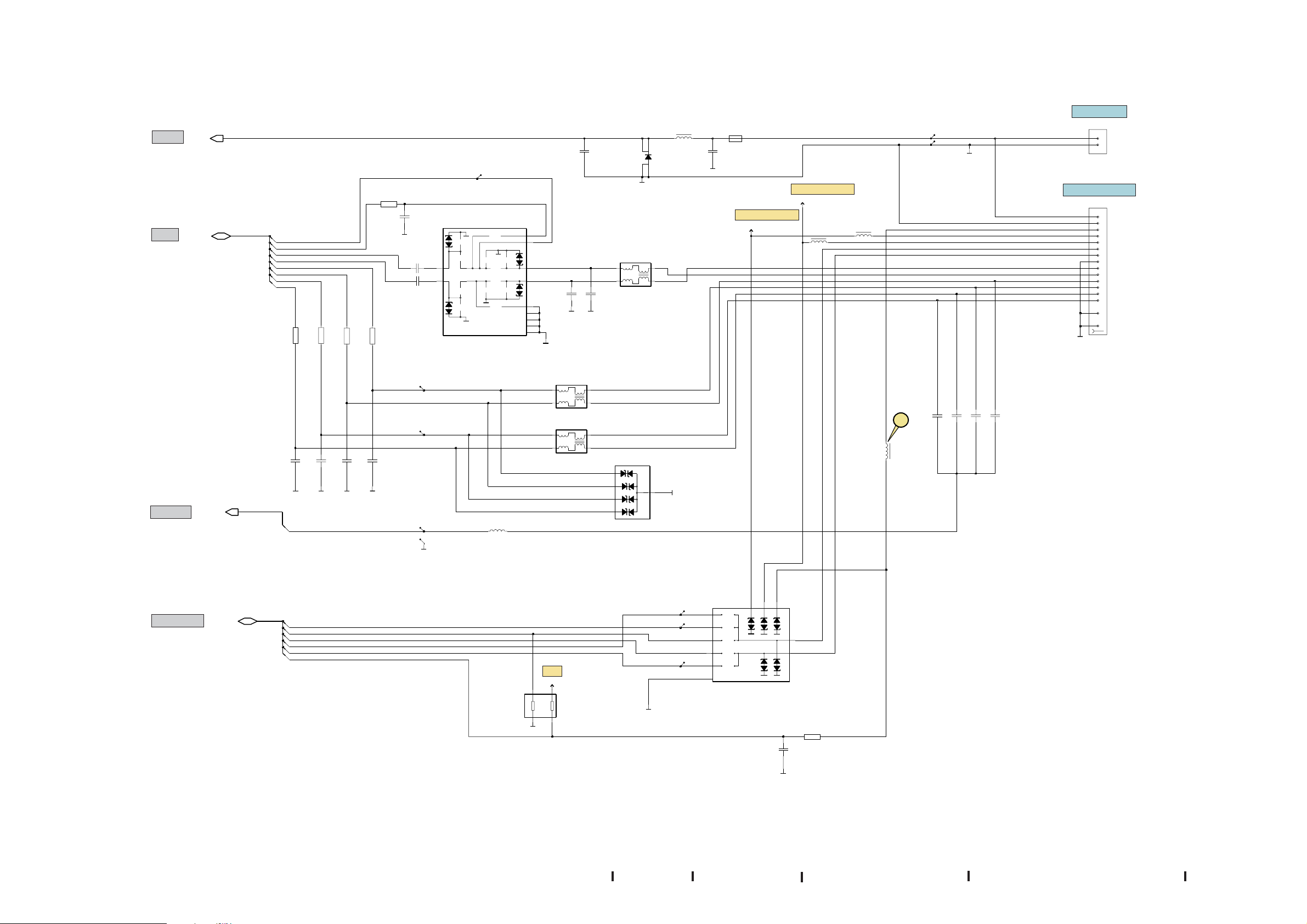
System connector
X2000
1
2
3
4
5
6
7
8
9
10
11
12
13
14
GND
AGND
GND
Retu, Tahvo
USB_ACI(7:0)
4
SLAVEPU
1
DPRXD
0
DMTXD
6
MASTPD2
5
MASTPD1
7
ACI
Customer Care / Training & Vendor Development/ Content Creation Team
Confidential - Copyright © 2006 NOKIA Only for training and service purposes
2.8V
VAUX
120k
220k
R2008
1 2
3 4
RESNET_220K_120K
GND
Version: 2.0 05.10.20
R2007
IP4065CX11_LF
J2007
J2008
J2009
GND
0
6
17k
1k3
33R
33R
15k
GND
C2015
220p
6085/ RM-198
R2009
220R
GND
Board version: 1VZ_12
System connector
Page 2 (9)

FM radio
RF part
RAPGSM
AUDIO(8:0)
SLOWAD(6:0)
DIG_AUDIO(5:0)
INT_SIM(5:0)
TXC(2:0)
ACI(1:0)
{
CBUS(3:0)
Battery connector
System connector
X2070
VBAT
GND
GND
R2100
EMIF01-SMIC01F2
C2 GND3
1n0
OUT
GND
C2231
-t
0
1
10U
C2307
GND
C2412
27p
C2072
27p
GND
0
2
1
0
2
1
220R/100MHz
L2205
GND
2u2
GND
VOUT
VBUS
R2200
C2202
0
1
2
3
4
5
220R/100MHz
C2232
1u0
A3
GND1
B3
C3
to Mic
B2
GND2
VREF_INT
100k
1n0
GND
L2202
GND
L2306
600R/100MHz
1.4V
1.8V
C2203
C2228
1n0
1n0
1u0
VCORE
VIO
50R
GND
GND
GND
Microphone
B2100
Power/End key
R2403
4k7
S2415
GND
3.7V
J2071
R2071
14V/50V
VBAT
C2071
27p
GND
GND
GND
J2070
BSI
J2072
BGND
CHARGER
C2074
10p
1
0
R2070
BTEMP NTC
+
GND
47k
C2073
150u/10V
GND
GND
2.5V (accessory connected)
5V (phone connected to host)
GND
C2306
1u0
C2304
2k2 2k2
2k2
14
10n
to Asic
1n0
GND3
50R
Vbias
150p1n0
C2205
1n0 1n0
GND
C2208
27p
GND
J2200
C2230
1u0
1
2
0
C2309
22u
GND
C2313
1u0
GND
C2206
GND
B1
C1
A2
2.5V1.35V
R2201
120k
C2207
GND
B2200
32.768kHz
23
0
1
2
L2301
220R/100MHz
R2307
MA21D34001JN
V2302
C2312
1u0
GND
1n0
C2225
100R
VANA
33n
C2100
C2101
33n
R2101
C2102
220R
2u2
GND
5
7
2.5V
C6190
C6191
100n
100n
VANA
GND
GND
C2224
C2223
R2213
R2214
4k7
4k7
C2204
1n0
1
GND
GND
C2209
R2216
2M2
22p
J2210
G2200
GND
J2212
GND
24
9810
C2281
1u0
GND
C2227
C2226
1u0
1u0
1u0
GND
GND
GND
C2300
C2310
10n
10u
GND
GND
C2302
22u
GND
R2300
4
CURRENT_SEN
BGND
10n
10n
GND
GND
+
-
GND
J2206
J2300
GND
L2302
10uH
E12
M12
F10
C2233
10u
GND
GND
J2204
J2205
M10
J2207
J2209
G10
C12
K11
K10
C2301
GND
22u
23
1
GND
GND
Retu
D2200
RETU_3.02
K1
Mic1P
J3
Mic1N
H1
MicB1
E1
Mic3P
E2
Mic3N
E3
Mic3PR
D2
Mic3NR
C3
VDARx
K2
VDATx
PwrOnX
BSI
L3
BTemp
M2
LS
L2
LST
M1
RFTemp
VChar
M3
WTxDet
L9
CrI
K9
CrO
L8
VBack
B6
SIMClk2
A6
SIMDa2
B7
SIMIOC2
J11
WDDis
M4
AudClk
A4
EarDaL
B4
EarDaR
B5
MicData
A3
PMARP
C4
PMARN
C5
SIMClk1
C6
SIMDa1
A5
SIMIOC1
M6
TxCClk
L7
TxCCtrl
L6
TxCDa
HV
L4
MBusTx
K4
MBusRx
M5
SerClk
L5
SerData
K5
SerSelX
VBat6
VBat1
VBat2
A8
VBat3
H12
VBat4
F12
VBat5
B12
VBatCP
B3
VBatH
ChSwS
Tahvo
N2300
TAHVO_V5.2_LF
J1
ChSwS
C1
CbusData
B1
CbusSelX
B2
CbusClk
D9
VCharADC
A7
VBAT1
A6
VBAT1
B5
GND1
A4
GND1
F10
VCharOut1
G10
VCharOut2
F9
VCharOutK
G9
VBAT3
D10
VCharIn1
E10
VCharIn2
E9
VCharInK
A5
VCoreCoil
B6
VCoreCoil
B4
VCore
H10
Vout
K10
VCC
A3
VIO
A10
NC
B10
NC
A8
NC
C10
NC
B8
NC
H2
SENSE-
G2
SENSE+
H3
H4
H5
H6
H7
H8
G3
G8
F3
F8
SLAVESWSET
NC
NC
NC
NC
NC
NC
NC
NC
NC
NC
HFSpP
HFSpN
HookDet
XEarLC
XEarRC
MicBCap
VSARx
MicSub
VDRAM
VRCP1
VRCP2
FlyHigh
SIMDaC1
SIMClkC1
SIMRstC1
SIMDetX
SIMClkC2
SIMDaC2
SIMRstC2
RetuInt
HeadDet
Slave_PU
Master_PD1
Master_PD2
D+_RXD
D-_TXD
VPP_VIO
RSTX
PURX
SLEEPX
SMPSClk
SleepClk
Clk600
VCCint
TahvoInt
GND3
GND4
GND5
PWM300
GenOut1
GenOut2
GenOut3
VcoreDef
FlashM
TestMode
TestOut
FSE0
RCV_FRX2
VP_FRX
VM_CLK
D3
EarP
D1
EarN
B1
C2
L12
J2
Mic2N
J1
Mic2P
F3
XEarL
F1
G1
XEarR
G3
H2
MicB2
G2
C1
H3
VSATx
F2
H10
VBG
F11
VRef
J12
VAna
E11
VAux
M11
D12
VIO
G11
VR1
G12
VRFC
C9
VSIM2
A10
C10
B10
VCP
B11
A12
FlyLow
M8
AFC
K7
TxC1
M7
TxC2
A7
VSIM1
C8
C7
C11
L1
B9
A9
D10
A2
VibraP
A1
VibraN
L10
TM
D11
Gnd1
K12
Gnd2
B8
Gnd3
K6
Gnd4
A11
GndCP
B2
GndH
K8
H11
MBus
L11
K3
PURX
M9
SlClk
E10
RstX
J10
SleepX
1.8V: active
0V: sleep mode
J10
H9
J9
J6
CLK
K7
RXD2
J7
K8
A1
B3
D2
D1
E1
E2
F1
K9
C2
J8
F2
A9
G1
J2
K1
H1
C9
A2
B7
B9
J4
OEX
K4
J5
VO
K2
J3
K3
K5
FTX
K6
E3
NC
E8
NC
D3
NC
D8
NC
C3
NC
C4
NC
C5
NC
C6
NC
C7
NC
C8
NC
GND
R2212
470R
C2303
0
1
6
2
4
3
15
7
0
C2200
GND
1u0
GND
GND
GND
C2201
GND
VRCP2
C2211
4u7
GND
GND
0
1
2
C2210
1u0
1u0
1.8/3V
J2216
J2217
3.7V
J2218
J2219
L2212
220R/100MHz
L2211
220R/100MHz
0
1
2
3
GND
GND
GND
GND
GND
GND
GND
J2208
1.8V
2
R2301
2
0
3
5
1
7
0
3k3
1
2
5
4
3
2
1
0
6
7
12
J2308
GND
1u0
GND
GND
GND
GND
GND
J2309
J2314
J2310
J2311
J2312
J2313
J2315
13
4.7V
C2221
1u0
0
L2270
27p
C2215
1u5
C2106
27p
GND
1.8V
VDRAM
C2219
1u5
GND
SIM Reader
Side
A2102
66
55
1QD
44
3
PWB VIBRA LIFTING
L2100
56nH
L2101
56nH
2.5V
2.8V
VAUX
VANA
C2217
C2216
1u5
1u5
GND
GND
C2700
GND
GND GND
GND
10
9
Vibra
8
7
3
7
VRCP1
GND
C2212
1u5
GND
220R/100MHz
L2271
220R/100MHz
}
C2222
1u0
C2274
C2270
1n0
C2105
C2272
C2271
1n0
1n0
GND
1u5
C2213
C2104
1.8V2.5V
VR1
C2214
1u5
GND
R2700
EMIF03-SIM02F2
C2103
10p10p
GND
VIO
GND
R1
R2
R3
1.8V
VRFC
C2220
1u5
GND
GND
C2273
1n0
C2275
27p27p
GND
Flash interface
J2060
RXD2
4
N2301
TPS61061YZFR
EN
SW
FB
ILED
1 2 3
PGND
GND
VPP
6 7 8
VBUS
4
5
6
3
2
1
0
22uH
L2305
600R/100MHz
C2305
1u0
C2317
C2315
27p
4u7
C2314
4u7
GND
GND
GND
GND
L2304
C1
OUT
B1
VIN
A1
GND
C3
Traceability pad
X2060
1
GND
1
RXD
CLK
TXD
LED driver
PWMTAHVO
A2
C2
B3
A3
GND
AUDIO(8:0)
A2100
1
3
4
IHF speaker
2
GND
1.35V
VREF_INT
VREF
SIM connector
X2701
470191501
1
2
3
100n
PUSL(7:0)
3.7V
VBAT
GND
7V (illumination active)
X2400
XAUDIO(7:0)
System connector
}
TXC_CONV(2:0)
5
6
7
USB_ACI(7:0)
System connector
RAPGSM, BT, FM radio
EMINT(1:0)
{
VLEDOUT1
Flip connector,
keyboard illumination
SETCURR1
INTUSB(8:0)
RF part
RAPGSM
GEN_OUT(3:0)
RAPGSM
UI
Customer Care / Training & Vendor Development/ Content Creation Team
Confidential - Copyright © 2006 NOKIA Only for training and service purposes
Version: 2.0 05.10.20
0
6085/ RM-198
6
Board version: 1VZ_12
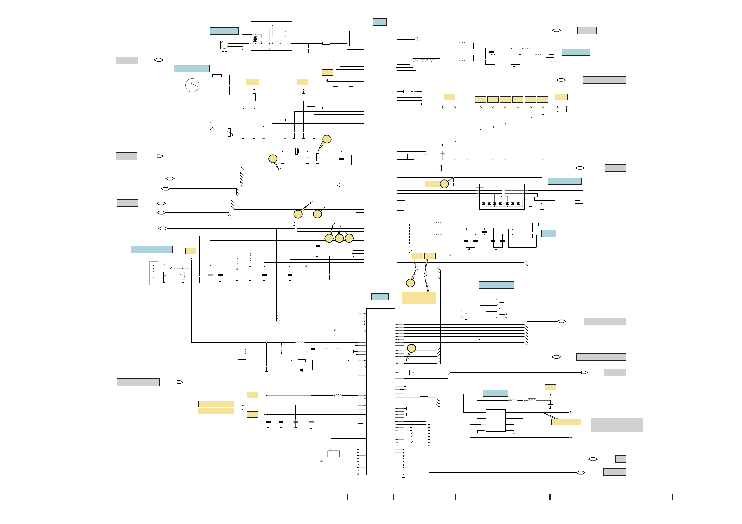
Retu, Tahvo, LED driver
Page 3 (9)
 Loading...