

Page 1

Programmes After Market Services (P.A.M.S.)
Technical Documentation
NME–2A SeriesTransceivers
Chapter 6
External SIM Card Reader
CAE–2
Original 08/97
Page 2

NME–2A
P.A.M.S.
External SIM Card Reader CAE–2
Technical Documentation
[This page intentionally left blank]
Page 6–2
Original 08/97
Page 3

P.A.M.S.
NME–2A
Technical Documentation
External SIM Card Reader CAE–2
Contents
Page No
Introduction 4
Summary 4
Modes of Operation 4
Card Out Mode 4
Card In Mode 5
Installation of the CAE–2 5
Block Description 6
Overview 6
Power Block 7
MBUS Interface 7
SIM Interface 7
MCU Block 8
Hardware Description 8
Signals on Modular Connectors 8
Signals on SIM Connector 9
Power Block 9
MBUS Interface 9
SIM Interface 10
MCU Block 11
Circuit Diagram of GM8S 12
Component Layout Diagram of GM8S 13
Parts List of CAE–2 (EDMS: Issue 4.2) 14
Exploded View of CAE–2 16
Mechanical Items 16
List of Figures
Figure 1: Interconnection Diagram 6
Figure 2: Block Diagram 7
Figure 3: Circuit Diagram of GM8S Module 12
Figure 4: Component Layout Diagram of GM8S 13
Figure 5: Exploded View of CAE–2 16
Original 08/97
Page 6–3
Page 4

NME–2A
P.A.M.S.
External SIM Card Reader CAE–2
Introduction
Summary
The CAE–2 external SIM card reader is designed for the Nokia 6081 GSM
car telephone with type designation NME–2A and the handset with type
designation HSE–6XA.
The card reader is designed for a ID–1 SIM card (IC–card) in accordance
with GSM recommendation 11.11 and ISO standard ISO–7816–1,2,3. All
cards which do not comply to the GSM11.11 and ISO–7816 will be
rejected by the CAE–2. Only one card at a time can be used in the
external card reader.
The card reader is connected to the telephone via the system cable and
an extension cable, through one of its modular connectors. The handset
is connected directly to the card reader through the second modular
connector. The two modular connectors are connected in parallel, so the
handset and the extension cable can be connected to any of the two
connectors.
Technical Documentation
The CAE–2 works in parallel with the internal card reader in the 6081. If a
card is inserted in the internal card reader, and there is no card in the
external, then the 6081 will function as normal. If a card is inserted in the
external card reader, and there is no card in the internal, then the 6081
will work as if a card was inserted in the internal reader. The external
reader has the highest priority, so if a SIM card is inserted in both the
internal and the external card reader, then the external will handle all the
GSM operations, and the internal SIM card interface will be disabled. If a
conversation already was established when a card is inserted in the
external card reader, that conversation is interrupted, the internal card
reader is disabled, and the telephone will log onto the network using the
SIM card in external reader.
Modes of Operation
The CAE–2 has two modes of operations which is, with or without a SIM
card inserted in the card reader.
Card Out Mode
Page 6–4
The card reader will be in this mode when no SIM card is inserted,
and 12V DC is connected via the modular connector, and this is the
case even if the MBUS connection is missing. The LED is
iluminated when the reader is in the card out mode.
Original 08/97
Page 5

P.A.M.S.
NME–2A
Technical Documentation
The card reader first sends a MBUS registration message (as a
slave unit) to the telephone (which is the master). The telephone
responds by sending a registration acknowledge message to the
card reader. When the acknowledge is received, the reader starts
looking for a SIM card. If the MBUS connection is missing it will
never start looking for a SIM card, because of the missing
registration acknowledge, so the LED will stay on even if a card is
inserted in the reader.
Card In Mode
When a SIM card is inserted in the reader, then the LED is turned
off, and it enters the card in mode. The card reader will do read
and write operations requested either from the telephone or SIM
card itself. All SIM operations, which are available from the user
interface in the telephone can can be done with a SIM card in the
internal card reader, can now be executed using the SIM card in
the external card reader. Phone calls can be initiated as soon as
the telephone is in service.
External SIM Card Reader CAE–2
If the SIM card is drawn out from the card reader, the SIM interface
will be disabled and the CAE–2 will enter the card out mode.
Installation of the CAE–2
The CAE–2 (10 is installed using a extension cable (11) which is plugged
into one of the modular connectors on the card reader and into the
connector on the system cable (5) normally used for the handset (2). The
handset is then connected to the second modular connector on the card
reader.
Original 08/97
Page 6–5
Page 6

NME–2A
P.A.M.S.
External SIM Card Reader CAE–2
Technical Documentation
After power up the system is ready for insertion of a SIM card. The SIM
card is inserted with the arrow on the SIM card facing the light guide for
the LED on the CAE–2. If the card is inserted upside down it will be
rejected by the card reader, and the message
written in the display of the handset. If this happens, draw out the SIM
card and insert it in the right way.
Block Description
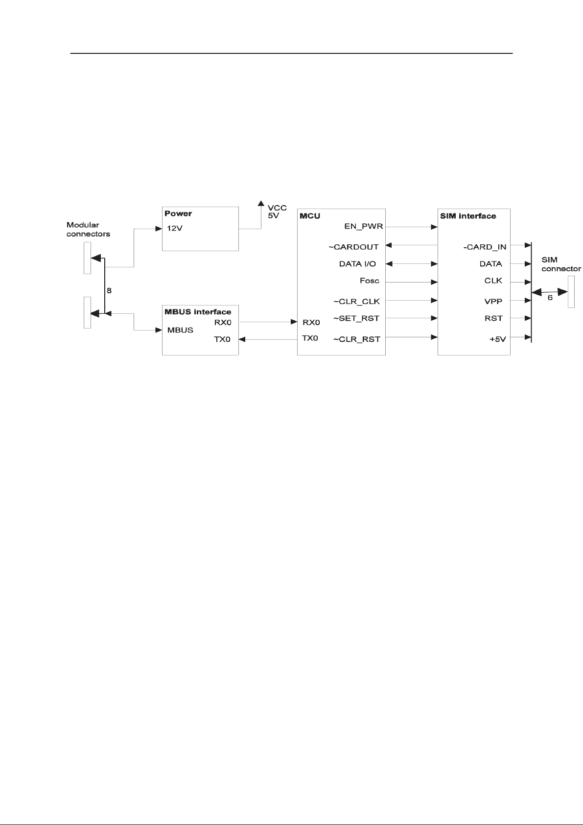
Overview
The card reader consists of four different blocks. A Power block, MBUS
interface, SIM interface and the MCU. The block diagram of the card
reader can be seen in figure 2.
Figure 1: Interconnection Diagram
CARD REJECTED
is
Page 6–6
Original 08/97
Page 7
P.A.M.S.
NME–2A
Technical Documentation
External SIM Card Reader CAE–2
Figure 2: Block Diagram
Power Block
The power block is responsible for converting the 12V DC from the
transceiver (see item 1 in figure 1) to 5V DC used for all the electronics in
the card reader except for the power to SIM card.
MBUS Interface
This block converts messages to the card reader on the bi–directional one
wire MBUS, to RX signals which can be read by the MCU. Messages
from the card reader to the transceiver, are also converted from the
MCU’s TX line to the bi–directional MBUS.
SIM Interface
The SIM card is provided with the prober signals in accordance with the
ISO 7816–3 standard through the SIM interface. It handles all control
signals from the MCU and do level shifting, power switching and clock
dividing for the SIM card. The +5V and VPP is controlled by the
~EN_PWR. RST can be set and reset by respectively ~SET_RST and
Original 08/97
Page 6–7
Page 8

NME–2A
P.A.M.S.
External SIM Card Reader CAE–2
~CLR_RST. DATA and DATA I/O is identical signals, and is the
bi–directional halfduplex data line on the SIM card. The CLK signal is
derived from the MCU oscillator Fosc. It can be stopped by the
~CLR_CLK signal. –CARD_IN is a sense input for SIM card insertion, and
it signals this event to the MCU trough the ~CARDOUT signal.
MCU Block
The MCU block consists mainly of the MCU which is controlling the card
reader. The LEDs used for operation mode indication is also part of this
block. The MCU has 2 UART’s, one for the SIM interface and one for the
MBUS interface. For explanation of the various signals to/from the MCU
block, see the two former paragraphs.
Hardware Description
Technical Documentation
The diagram in the
for this description of the hardware.
Signals on Modular Connectors
The modular connectors are wired in parallel and the various signals on
these connectors (and the system cable and handset cable) is shown in
the following table. All signals in bold are used in the card reader.
PIN NAME SIGNAL EXPLANATION
1 HS LSP Loudspeaker (not used)
2 ON/OFF KEY Power switch (not used)
3 MBUS Bi–directional data line
4 AGND Audio ground (not used)
5 DGND Digital ground
6 HS MIC Microphone (not used)
7 12V DC Vbat_sw from transceiver
8 EARPHONE Earphone (not used)
Schematic – detailed
paragraph is used as the basis
Page 6–8
Original 08/97
Page 9

P.A.M.S.
NME–2A
Technical Documentation
Signals on SIM Connector
The SIM card is connected via the X3 flex foil connector.
PIN NAME SIGNAL EXPLANATION
1 –CARD_IN SIM insertion sense. Connected
2 +CARD_IN VCC for hw switch in card reader
3 DATA Bi–directional half–duplex SIM
4 CLK Clock signal for SIM card
5 VPP Programming voltage for SIM
6 RST Reset signal to SIM card
7 GND Ground for SIM card. Connected
8 +5V Power for SIM card
External SIM Card Reader CAE–2
to hw switch in card reader
mechanics.
mechanics
data line
card
to DGND
Power Block
The power block consists of a low dropout voltage regulator LP2951ACM
(N1), used for converting the incomming 12V DC (Vbat_sw) from the
transceiver to the VCC (5V DC) used for all the electronics in the card
reader, except the DC power connection for the SIM card.
SIGNAL IN/OUT VALUE MIN MAX
12V In 12V DC current 1.5A 10.8 V DC 15.6 V DC
VCC Out 5V DC 100mA 4.93 V DC 5.07 V DC
MBUS Interface
The MBUS is used for communications between all the units. It is a
bi–directional halfduplex signal line, with a transmission speed of 9600
baud. The MBUS signal is converted to RX signal to the MCU and TX
signal from the MCU via the sense resistor R19 and the open collector
output made by transistor V4 and inverter V5. The pull–up resistor for the
MBUS is placed in the transceiver. It also includes the EMC filter for the
MBUS line.
Original 08/97
Page 6–9
Page 10

NME–2A
P.A.M.S.
External SIM Card Reader CAE–2
SIM Interface
The SIM interface is responsible for generating all the necessary signal for
the SIM card. It is controlled by the MCU block. It consists of three parts.
A power switch made by V2, a divide by 2 for the SIM clock made by
toggle D–FF D1 and a D–FF used as a set/reset handler for the SIM reset
signal. The HC74 D–FF is also necessary for converting the output levels
of the MCU to the signal levels needed by the SIM card. The SIM
interface also includes the EMC filters for the SIM connections.
The D1a D–FF divide the MCU oscillator frequency of 7.3728 Mhz to
3.6864 Mhz which is used as SIM clock. The SIM clock can be disabled
by the MCU signal ~CLR_CLK and it will always stop on a low value (’0’).
The clock should have a duty cycle of 45% to 55% and a rise and fall time
of not more than 24 ns. When the power to the SIM is removed, the reset
input of the CLK FF is kept at a low signal via another switch.
Technical Documentation
The D1b D–FF controls the reset signal (RST) for the SIM card. The RST
can be set by the MCU signal ~CLR_RST and set by ~SET_RST. It will
also be in reset state when power is removed from the SIM card.
The _CARD_IN signal is low when there is no SIM card inserted. The
~CARD_IN will raise to a high (’1’) if a SIM card is inserted. The inserted
SIM card will shunt a mechanical switch, which is connected at the flex foil
connector X3’s pin 1 and 2. The –CARD_IN signal is used as a output
signal from the SIM interface to the MCU where it is called ~CARDOUT.
The transistor V2 is used as a power switch for the SIM card. It is
controlled by the MCU signal ~EN_PWR. The output +5V is supplying
both the VPP and the VCC pin on the SIM card. The regulation on the
+5V is supplying both the VPP and the VCC pin on the SIM card. The
regulation on the +5V must not fall below 4.5 V DC.
The ~EN_PWR signal also controls 3 HC4066 switches. Two of them are
used to reset the RST and CLK FF’s, when no power is applied to the SIM
card. The third is grounding the SIM DATA line when the power is
removed, in conjunction with R10. R10 serves as a pull up resistor when
power is applied to the SIM card, and a pull down when power is
removed.
Page 6–10
When power is applied to the SIM card the HC4066 switch in the SIM
DATA line is activated, and the MCU’s RX and TX is connected to the SIM
card.
For all the different signal levels on the SIM interface, see the ISO 7816–3
standard.
Original 08/97
Page 11

P.A.M.S.
NME–2A
Technical Documentation
MCU Block
The MCU is a DS87C520 from Dallas Semiconducters. It controls the SIM
and MBUS interface, and all communications with the two interfaces is
done with respectively UART 1 and UART 0. The MCU handles the
power up reset automatically, and it also monitors the VCC in order to
disable the SIM interface in case of a low voltage on VCC (<4.25 VDC).
Without any SIM card inserted in card reader the LED’s V6 and V7 will be
turned on by the MCU. Approx 9 mA is used for the LED’s. If a SIM card
is inserted the MCU will turn off the LED’s and enable the SIM interface in
accordance with the ISO 7816–3 standard.
In the following table an explanation of the signals in the MCU block is
given.
SIGNAL IN/OUT EXPLANATION
External SIM Card Reader CAE–2
~TEST In Only for test purposes
~SET_RST Out When low, the RST on SIM is
high
~CLR_RST Out When low, the RST on SIM is
low
~CLR_CLK Out When low, the clock for SIM card
is stopped at a low value
~EN_PWR Out Enables the +5V DC for the SIM
card
~CARDOUT In A low on this will interrupt the
MCU, and indicate that the SIM
card is removed
RX1 In SIM data is received via this pin
TX1 Out MCU transmit data to the SIM
card via this pin
INTO In Used for software purposes
P1.4 In Used for software purposes
RX0 In MBUS messages are received
via this pin
TX0 Out MCU transmit to MBUS via this
pin
T2EX In Used for software purposes
P1.6 Out LED controlling pin
Original 08/97
Page 6–11
Page 12

NME–2A
P.A.M.S.
External SIM Card Reader CAE–2
Circuit Diagram of GM8S
Technical Documentation
Page 6–12
Original 08/97
Page 13

P.A.M.S.
NME–2A
Technical Documentation
Layout Diagram
External SIM Card Reader CAE–2
Original 08/97
Page 6–13
Page 14

NME–2A
P.A.M.S.
External SIM Card Reader CAE–2
Technical Documentation
Parts List of CAE–2 (EDMS: Issue 4.2)
ITEM CODE DESCRIPTION VALUE TYPE
––––––––––––––––––––––––––––––––––––––––––––––––––––––––
R001 1430151 Chip resistor 10 5 % 0.063 W 0603
R002 1430087 Chip resistor 100 k 5 % 0.063 W 0603
R003 1430065 Chip resistor 10 k 5 % 0.063 W 0603
R006 1430087 Chip resistor 100 k 5 % 0.063 W 0603
R008 1430065 Chip resistor 10 k 5 % 0.063 W 0603
R009 1430065 Chip resistor 10 k 5 % 0.063 W 0603
R010 1430065 Chip resistor 10 k 5 % 0.063 W 0603
R011 1430298 Chip resistor 1.0 M 2 % 0.063 W 0603
R012 1430071 Chip resistor 22 k 5 % 0.063 W 0603
R016 1430071 Chip resistor 22 k 5 % 0.063 W 0603
R017 1430087 Chip resistor 100 k 5 % 0.063 W 0603
R018 1430087 Chip resistor 100 k 5 % 0.063 W 0603
R021 1430144 Chip jumper 0603
R022 1430144 Chip jumper 0603
R030 1430087 Chip resistor 100 k 5 % 0.063 W 0603
R031 1430065 Chip resistor 10 k 5 % 0.063 W 0603
C001 2604103 Tantalum cap. 4.7 u 20 % 35 V 7.3x4.4x2.8
C002 2310784 Ceramic cap. 100 n 10 % 25 V 0805
C003 2320059 Ceramic cap. 100 p 5 % 50 V 0603
C004 2320107 Ceramic cap. 10 n 5 % 50 V 0603
C005 2310784 Ceramic cap. 100 n 10 % 25 V 0805
C006 2310784 Ceramic cap. 100 n 10 % 25 V 0805
C007 2604431 Tantalum cap. 10 u 20 % 16 V 6.0x3.2x2.5
C008 2320045 Ceramic cap. 27 p 5 % 50 V 0603
C009 2320045 Ceramic cap. 27 p 5 % 50 V 0603
C010 2320045 Ceramic cap. 27 p 5 % 50 V 0603
C011 2320059 Ceramic cap. 100 p 5 % 50 V 0603
C012 2320059 Ceramic cap. 100 p 5 % 50 V 0603
C013 2320059 Ceramic cap. 100 p 5 % 50 V 0603
C014 2320059 Ceramic cap. 100 p 5 % 50 V 0603
C015 2320059 Ceramic cap. 100 p 5 % 50 V 0603
C016 2320045 Ceramic cap. 27 p 5 % 50 V 0603
C017 2310784 Ceramic cap. 100 n 10 % 25 V 0805
C018 2320059 Ceramic cap. 100 p 5 % 50 V 0603
B001 4510036 Crystal 7.3728 M +–50PPM 12x6x3mm
V002 4200909 TransistorBC858B/BCW30 pnp 30 V 100 mA SOT23
V003 4200917 TransistorBC848B/BCW32 npn 30 V 100 mA SOT23
Page 6–14
Original 08/97
Page 15

P.A.M.S.
NME–2A
Technical Documentation
V004 4200917 TransistorBC848B/BCW32 npn 30 V 100 mA SOT23
V005 4200917 TransistorBC848B/BCW32 npn 30 V 100 mA SOT23
V006 4102998 Led Green 2.2 V 1206
V007 4102998 Led Green 2.2 V 1206
D001 4309375 IC, 2 x D–flip–flop 74HC74 SO14S
D002 4309488 IC, 4 x bi.switch 74HC4066 SO14S
N001 4301062 IC, regulator LP2951AC SO8S
N002 0240426 MCU SW Module
4370169 MCU DS87C520
8400470 ROM Code
9380149 Sticker Brady LAT–2–747 9.5X9.5
X001 5416518 Modular jack 8 pole smd
X002 5416518 Modular jack 8 pole smd
X003 5431702 Flexfoil connect 1x08 1mm smd
P001 9854153 PC board GM8S 80.8x58.2x1.6 d 4/pa
9854153 PCB GM8S 80.8X58.2X1.6 D 4/PA
External SIM Card Reader CAE–2
Original 08/97
Page 6–15
Page 16

NME–2A
P.A.M.S.
External SIM Card Reader CAE–2
Exploded View of CAE–2
Technical Documentation
Figure 5: Exploded View of CAE–2
Mechanical Items
ITEM CODE DESCRIPTION VALUE TYPE
1 9450019 Front Cover CAE–2 1D21141
2 9450018 Bottom Cover CAE–2 3D21142
3 9450017 Light Guide CAE–2 3D21143
4 6292279 PT–screw KB30x10 WN1442
FEXN BLU
5 9380154 Label blank 4D21745
6 5408803 Chip card reader push
7 6291917 PT–screw KB25x5 WN1442
8 9380112 Cover sticker 4D21434
S1 0201013 GM8S module
Page 6–16
Original 08/97
 Loading...