

Page 1

PAMS Technical Documentation
NME-2A Series T ransceivers
Chapter 4
System Module GM8
Issue 2 05/2000 Nokia Mobile Phones Ltd.
Page 2
NME-2A
System Module GM8
PAMS Technical Documentation
AMENDMENT RECORD SHEET
Amendment
Number
Date Inserted By Comments
08/97 Original
Issue 2 02/2000 OJuntune ARS added
TOC updated
New layout for tables
Parts list v.4.3 added
repaginated
A3 schematics for v. 13 added
Page 2
Nokia Mobile Phones Ltd.
Issue 2 05/2000
Page 3

PAMS Technical Documentation
System Module GM8
CHAPTER 4 – SYSTEM MODULE GM8
CONTENTS
Introduction 7. . . . . . . . . . . . . . . . . . . . . . . . . . . . . . . . . . . . . . . . . . . . . . . . . . . . . .
Technical Specifications 7. . . . . . . . . . . . . . . . . . . . . . . . . . . . . . . . . . . . . . . . . . .
Modes of Operation 7. . . . . . . . . . . . . . . . . . . . . . . . . . . . . . . . . . . . . . . . . . .
External and Internal Connections 8. . . . . . . . . . . . . . . . . . . . . . . . . . . . . . .
System Connector 8. . . . . . . . . . . . . . . . . . . . . . . . . . . . . . . . . . . . . . . . . .
SIM Card Reader 9. . . . . . . . . . . . . . . . . . . . . . . . . . . . . . . . . . . . . . . . . .
Data Connector 10. . . . . . . . . . . . . . . . . . . . . . . . . . . . . . . . . . . . . . . . . . . .
Internal Signals 11. . . . . . . . . . . . . . . . . . . . . . . . . . . . . . . . . . . . . . . . . . . .
Baseband Block Description 14. . . . . . . . . . . . . . . . . . . . . . . . . . . . . . . . . . . . . . .
General 14. . . . . . . . . . . . . . . . . . . . . . . . . . . . . . . . . . . . . . . . . . . . . . . . . . . . . .
NME-2A
Names of Functional Blocks 14. . . . . . . . . . . . . . . . . . . . . . . . . . . . . . . . . . . .
Clocking Scheme 15. . . . . . . . . . . . . . . . . . . . . . . . . . . . . . . . . . . . . . . . . . . . .
Reset and Power Control 16. . . . . . . . . . . . . . . . . . . . . . . . . . . . . . . . . . . . . . .
Watchdog System 17. . . . . . . . . . . . . . . . . . . . . . . . . . . . . . . . . . . . . . . . . . . . .
CTRLU 18. . . . . . . . . . . . . . . . . . . . . . . . . . . . . . . . . . . . . . . . . . . . . . . . . . . . . .
Main Components 18. . . . . . . . . . . . . . . . . . . . . . . . . . . . . . . . . . . . . . . . . .
Input Signals of CTRLU 19. . . . . . . . . . . . . . . . . . . . . . . . . . . . . . . . . . . . .
Output Signals of CTRLU 20. . . . . . . . . . . . . . . . . . . . . . . . . . . . . . . . . . .
Bidirectional Signals of CTRLU 20. . . . . . . . . . . . . . . . . . . . . . . . . . . . . . .
Block Description 20. . . . . . . . . . . . . . . . . . . . . . . . . . . . . . . . . . . . . . . . . . .
PWRU 22. . . . . . . . . . . . . . . . . . . . . . . . . . . . . . . . . . . . . . . . . . . . . . . . . . . . . . .
Main Components 22. . . . . . . . . . . . . . . . . . . . . . . . . . . . . . . . . . . . . . . . . .
Input Signals of PWRU 22. . . . . . . . . . . . . . . . . . . . . . . . . . . . . . . . . . . . . .
Output Signals of PWRU 23. . . . . . . . . . . . . . . . . . . . . . . . . . . . . . . . . . . .
Block Description 23. . . . . . . . . . . . . . . . . . . . . . . . . . . . . . . . . . . . . . . . . . .
DSPU 24. . . . . . . . . . . . . . . . . . . . . . . . . . . . . . . . . . . . . . . . . . . . . . . . . . . . . . .
Main Components of DSPU 25. . . . . . . . . . . . . . . . . . . . . . . . . . . . . . . . .
Input Signals of DSPU 26. . . . . . . . . . . . . . . . . . . . . . . . . . . . . . . . . . . . . .
Output Signals of DSPU 26. . . . . . . . . . . . . . . . . . . . . . . . . . . . . . . . . . . . .
Bidirectional Signals of DSPU 26. . . . . . . . . . . . . . . . . . . . . . . . . . . . . . . .
Block Description of DSPU 27. . . . . . . . . . . . . . . . . . . . . . . . . . . . . . . . . .
AUDIO 27. . . . . . . . . . . . . . . . . . . . . . . . . . . . . . . . . . . . . . . . . . . . . . . . . . . . . . .
Main Components of AUDIO 28. . . . . . . . . . . . . . . . . . . . . . . . . . . . . . . . .
Input Signals of AUDIO 28. . . . . . . . . . . . . . . . . . . . . . . . . . . . . . . . . . . . .
Output Signals of AUDIO 28. . . . . . . . . . . . . . . . . . . . . . . . . . . . . . . . . . . .
Issue 2 05/2000
Nokia Mobile Phones Ltd.
Page 3
Page 4

NME-2A
System Module GM8
Block Description of AUDIO 29. . . . . . . . . . . . . . . . . . . . . . . . . . . . . . . . .
ASIC 29. . . . . . . . . . . . . . . . . . . . . . . . . . . . . . . . . . . . . . . . . . . . . . . . . . . . . . . .
Main Components of ASIC 29. . . . . . . . . . . . . . . . . . . . . . . . . . . . . . . . . .
Input Signals of ASIC 30. . . . . . . . . . . . . . . . . . . . . . . . . . . . . . . . . . . . . . .
Output Signals of ASIC 30. . . . . . . . . . . . . . . . . . . . . . . . . . . . . . . . . . . . .
Bidirectional Signals of ASIC 32. . . . . . . . . . . . . . . . . . . . . . . . . . . . . . . . .
Block Description of ASIC 32. . . . . . . . . . . . . . . . . . . . . . . . . . . . . . . . . . .
RFI 33. . . . . . . . . . . . . . . . . . . . . . . . . . . . . . . . . . . . . . . . . . . . . . . . . . . . . . . . . .
Main Components of RFI 33. . . . . . . . . . . . . . . . . . . . . . . . . . . . . . . . . . . .
Input Signals of RFI 34. . . . . . . . . . . . . . . . . . . . . . . . . . . . . . . . . . . . . . . .
Output Signals of RFI 34. . . . . . . . . . . . . . . . . . . . . . . . . . . . . . . . . . . . . . .
Bidirectional Signals of RFI 34. . . . . . . . . . . . . . . . . . . . . . . . . . . . . . . . . .
Block Description of RFI 34. . . . . . . . . . . . . . . . . . . . . . . . . . . . . . . . . . . . .
PAMS Technical Documentation
RF Block Description 36. . . . . . . . . . . . . . . . . . . . . . . . . . . . . . . . . . . . . . . . . . . . .
Regulators 36. . . . . . . . . . . . . . . . . . . . . . . . . . . . . . . . . . . . . . . . . . . . . . . . . . .
Power Distribution 36. . . . . . . . . . . . . . . . . . . . . . . . . . . . . . . . . . . . . . . . . . . . .
Current Consumption 36. . . . . . . . . . . . . . . . . . . . . . . . . . . . . . . . . . . . . . . . . .
Receiver 37. . . . . . . . . . . . . . . . . . . . . . . . . . . . . . . . . . . . . . . . . . . . . . . . . . . . .
Duplex Filter 37. . . . . . . . . . . . . . . . . . . . . . . . . . . . . . . . . . . . . . . . . . . . . . .
Pre–Amplifier 38. . . . . . . . . . . . . . . . . . . . . . . . . . . . . . . . . . . . . . . . . . . . . .
RX Interstage Filters 38. . . . . . . . . . . . . . . . . . . . . . . . . . . . . . . . . . . . . . . .
Second LNA 39. . . . . . . . . . . . . . . . . . . . . . . . . . . . . . . . . . . . . . . . . . . . . . .
First Mixer 39. . . . . . . . . . . . . . . . . . . . . . . . . . . . . . . . . . . . . . . . . . . . . . . . .
First IF Amplifier 40. . . . . . . . . . . . . . . . . . . . . . . . . . . . . . . . . . . . . . . . . . .
First IF Filter 40. . . . . . . . . . . . . . . . . . . . . . . . . . . . . . . . . . . . . . . . . . . . . . .
AGC Amplifier 41. . . . . . . . . . . . . . . . . . . . . . . . . . . . . . . . . . . . . . . . . . . . .
Receiver IF IC 41. . . . . . . . . . . . . . . . . . . . . . . . . . . . . . . . . . . . . . . . . . . . .
Second IF Filter 42. . . . . . . . . . . . . . . . . . . . . . . . . . . . . . . . . . . . . . . . . . . .
Second IF Amplifier 42. . . . . . . . . . . . . . . . . . . . . . . . . . . . . . . . . . . . . . . . .
Phase Split 43. . . . . . . . . . . . . . . . . . . . . . . . . . . . . . . . . . . . . . . . . . . . . . . .
Page 4
Transmitter 44. . . . . . . . . . . . . . . . . . . . . . . . . . . . . . . . . . . . . . . . . . . . . . . . . . .
Modulator Circuit 44. . . . . . . . . . . . . . . . . . . . . . . . . . . . . . . . . . . . . . . . . . .
Up Conversion Mixer 45. . . . . . . . . . . . . . . . . . . . . . . . . . . . . . . . . . . . . . .
TX Interstage Filters 46. . . . . . . . . . . . . . . . . . . . . . . . . . . . . . . . . . . . . . . .
TX Amplifiers 46. . . . . . . . . . . . . . . . . . . . . . . . . . . . . . . . . . . . . . . . . . . . . .
Power Amplifier 47. . . . . . . . . . . . . . . . . . . . . . . . . . . . . . . . . . . . . . . . . . . .
Power Control Circuitry 47. . . . . . . . . . . . . . . . . . . . . . . . . . . . . . . . . . . . .
Frequency Synthesizers 48. . . . . . . . . . . . . . . . . . . . . . . . . . . . . . . . . . . . . . . .
Nokia Mobile Phones Ltd.
Issue 2 05/2000
Page 5

PAMS Technical Documentation
VCTCXO 48. . . . . . . . . . . . . . . . . . . . . . . . . . . . . . . . . . . . . . . . . . . . . . . . . .
VHF PLL 49. . . . . . . . . . . . . . . . . . . . . . . . . . . . . . . . . . . . . . . . . . . . . . . . . .
VHF VCO 49. . . . . . . . . . . . . . . . . . . . . . . . . . . . . . . . . . . . . . . . . . . . . . . . .
UHF Synthesizer 50. . . . . . . . . . . . . . . . . . . . . . . . . . . . . . . . . . . . . . . . . . .
UHF VCO 50. . . . . . . . . . . . . . . . . . . . . . . . . . . . . . . . . . . . . . . . . . . . . . . . .
UHF VCO Buffer 51. . . . . . . . . . . . . . . . . . . . . . . . . . . . . . . . . . . . . . . . . . .
PLL Circuit 51. . . . . . . . . . . . . . . . . . . . . . . . . . . . . . . . . . . . . . . . . . . . . . . .
Prescaler 52. . . . . . . . . . . . . . . . . . . . . . . . . . . . . . . . . . . . . . . . . . . . . . . . . .
Part List of GM8 (EDMS Issue: 2.6) 58. . . . . . . . . . . . . . . . . . . . . . . . . . . . . . . .
Part List of GM8 v.13 (EDMS Issue: 3.4) 78. . . . . . . . . . . . . . . . . . . . . . . . . . . .
System Module GM8
List of Figures
Clocking Scheme 4 – 14. . . . . . . . . . . . . . . . . . . . . . . . . . . . . . . . . . . . . . . . . . . . . . . .
Reset & Power Control 4 – 15. . . . . . . . . . . . . . . . . . . . . . . . . . . . . . . . . . . . . . . . . . . .
NME-2A
Watchdog System 4 – 16. . . . . . . . . . . . . . . . . . . . . . . . . . . . . . . . . . . . . . . . . . . . . . . .
Interconnection Diagram – Baseband 4 – 52. . . . . . . . . . . . . . . . . . . . . . . . . . . . . . .
Power Distribution Diagram – Baseband 4 – 53. . . . . . . . . . . . . . . . . . . . . . . . . . . .
Block Diagram – Diagram of RF 4 – 54. . . . . . . . . . . . . . . . . . . . . . . . . . . . . . . . . . . .
Power Distribution – Diagram of RF 4 – 55. . . . . . . . . . . . . . . . . . . . . . . . . . . . . . . .
Interconnections – RF and BB 4 – 56. . . . . . . . . . . . . . . . . . . . . . . . . . . . . . . . . . . . .
A3:
Block Diagram of Baseband (Version 1.0 Edit 192) 4/A3–1. . . . . . . . . .
Circuit Diagram of MCU & Memories (Version 1.0 Edit 3) 4/A3–2. . . .
Circuit Diagram of Power Supply (Version 1.0 Edit 16) 4/A3–3. . . . . .
Circuit Diagram of DSPU (Version 1.0 Edit 4) 4/A3–4. . . . . . . . . . . . . .
Circuit Diagram of Audio (Version 1.0 Edit 6) 4/A3–5. . . . . . . . . . . . . .
Circuit Diagram of ASIC (Version 1.0 Edit 15) 4/A3–6. . . . . . . . . . . . . .
Circuit Diagram of RFI (Version 1.0 Edit 3) 4/A3–7. . . . . . . . . . . . . . . . .
Block Diagram of RF (Version 1.0 Edit 70) 4/A3–8. . . . . . . . . . . . . . . . .
Circuit Diagram of Receiver (Version 1.0 Edit 208) 4/A3–9. . . . . . . . . .
Circuit Diagram of Transmitter (Version 4.3 Edit 220) 4/A3–10. . . . . . . .
Circuit Diagram of Synthesizers (Version 0.0 Edit 116) 4/A3–11. . . . . .
Component Layout Diagram of Side 1 4/A3–12. . . . . . . . . . . . . . . . . . . . .
Component Layout Diagram of Side 2 4/A3–13. . . . . . . . . . . . . . . . . . . . .
Block Diagram of Baseband v.13( 1.0 Edit 192) 4/A3–1. . . . . . . . . . . . .
Circuit Diagram of MCU & Memories (Version 1.0 Edit 3) 4/A3–2. . . .
Issue 2 05/2000
Nokia Mobile Phones Ltd.
Page 5
Page 6

NME-2A
System Module GM8
Circuit Diagram of Power Supply (Version 1.0 Edit 16) 4/A3–3. . . . . .
Circuit Diagram of DSPU (Version 1.0 Edit 4) 4/A3–4. . . . . . . . . . . . . .
Circuit Diagram of Audio (Version 1.0 Edit 6) 4/A3–5. . . . . . . . . . . . . .
Circuit Diagram of ASIC (Version 1.0 Edit 15) 4/A3–6. . . . . . . . . . . . . .
Circuit Diagram of RFI (Version 1.0 Edit 3) 4/A3–7. . . . . . . . . . . . . . . . .
Block Diagram of RF (Version 1.0 Edit 70) 4/A3–8. . . . . . . . . . . . . . . . .
Circuit Diagram of Receiver (Version 1.0 Edit 208) 4/A3–9. . . . . . . . . .
Circuit Diagram of Transmitter (Version 4.3 Edit 220) 4/A3–10. . . . . . . .
Circuit Diagram of Synthesizers (Version 0.0 Edit 116) 4/A3–11. . . . . .
Component Layout Diagram of Side 1 4/A3–12. . . . . . . . . . . . . . . . . . . . .
Component Layout Diagram of Side 2 4/A3–13. . . . . . . . . . . . . . . . . . . . .
V.13 diagrams (A3):
PAMS Technical Documentation
Block Diagram of Baseband, version 13 (V.1 Edit 280) 4.1/A3–1. . . . . . .
Circuit Diagram of MCU & Memories, version 13 (V.1 Edit 10) 4.1/A3–2
Circuit Diagram of Power Supply, version 13 (V.1 Edit 25) 4.1/A3–3. . .
Circuit Diagram of DSPU, version 13 (V.1 Edit 10) 4.1/A3–4. . . . . . . . . .
Circuit Diagram of Audio, version 13 (V.1 Edit 15) 4.1/A3–5. . . . . . . . .
Circuit Diagram of ASIC, version 13 (V.1 Edit 21) 4.1/A3–6. . . . . . . . . .
Circuit Diagram of RFI, version 13 (V.1 Edit 9) 4.1/A3–7. . . . . . . . . . . . .
Block Diagram of RF, version 13 (V.1 Edit 77) 4.1/A3–8. . . . . . . . . . . . .
Circuit Diagram of Receiver, version 13 (V.1 Edit 219) 4.1/A3–9. . . . . .
Circuit Diagram of Transmitter, version 13 (V.4.3 Edit 239) 4.1/A3–10. .
Circuit Diagram of Synthesizers, version 13 (V.0.0 Edit 123) 4.1/A3–11.
Component Layout Diagram of GM8 v.13 Side 1 4.1/A3–12. . . . . . . . . . . .
Component Layout Diagram of GM8 v.13 Side 2 4.1/A3–13. . . . . . . . . . . .
Page 6
Nokia Mobile Phones Ltd.
Issue 2 05/2000
Page 7

PAMS Technical Documentation
Introduction
System Module GM8 is the baseband/RF module NME–2A cellular
tranceiver. The GM8 module carries out all the system and RF functions of
the tranceiver. System module GM8 is designed for a mobile phone, that
operate in GSM system.
Technical Specifications
The entire transceiver is built on a single multilayer PWB. This board is
enclosed in a housing consisting of a metal bottom part and a metallized
top plastic part. The housing has walls to separate baseband from RF.
Modes of Operation
There are three different operation modes:
– active mode
NME-2A
System Module GM8
– idle mode
– power off mode
In the active state all circuits are powered and part of the module may be
in idle mode.
The module is usually in the idle mode when there is no call and the
phone is in SERV. In the idle mode circuits are reset, powered down and
clocks are stopped or the frequency reduced. All the clocks except the
main clock from VCTCXO can be stopped in that mode. Whether the SIM
clock is stopped or not depends on the network.
Currently the MCU only goes into sleep mode when in IDLE, not to MCU
standby mode as the time to wake the SW is too long.
In power off mode all circuits are disabled. Power is turned on and off by
pressing the
the transceiver. The power FET enables power to the handset and the
transceiver.
The Ignition Sense circuit will (when connected) turn the phone on when
IGNS input goes high. This circuit is active for approximately 200ms.
which is ample time for the phone to turn on.
on/off
key on the handset which activates a power FET on
Issue 2 05/2000
Nokia Mobile Phones Ltd.
Page 7
Page 8
NME-2A
TENNA
System Module GM8
External and Internal Connections
The transceiver has three connectors, a 25 pole connector which basically
implements the VDA recommendation for a GSM mobile phone, the
antenna connector and a 16 pole connector for the Data Transfer
implementing the M2BUS, the D–BUS and Flash programming. All internal
connections on the board are by PWB wiring. The SIM card reader is
soldered to the board.
System Connector
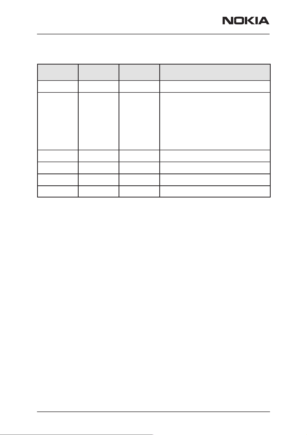
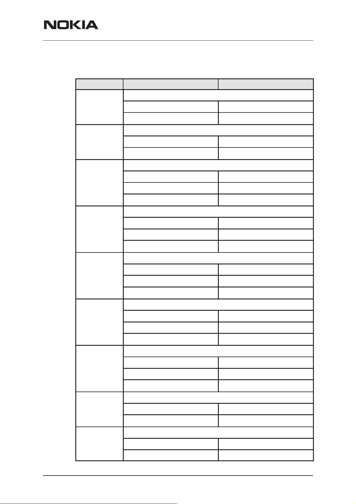
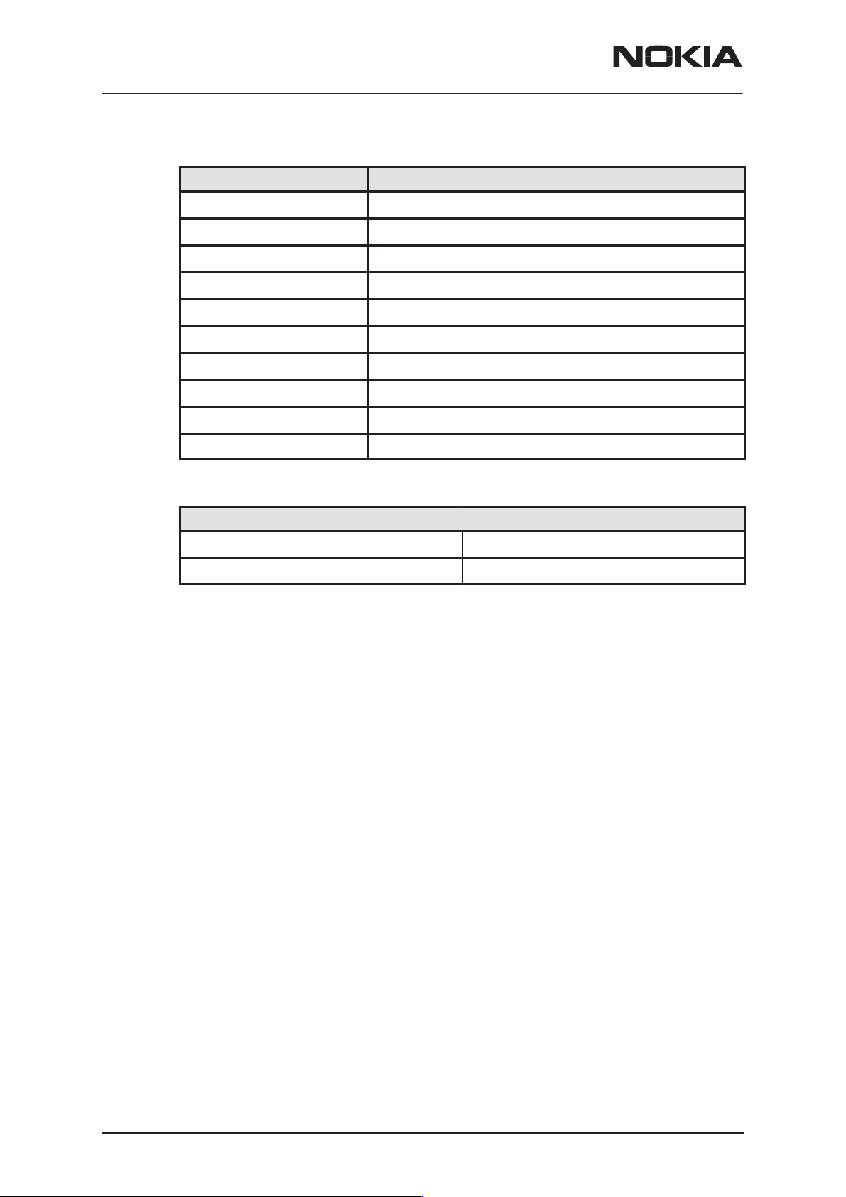
Pin Name Description
1 MIC Handset mic
2 NC Not used
3, 17 RFGND Battery GND
4, 16 VBATT Battery voltage
PAMS Technical Documentation
• nominal voltage:
5 IGNS IGNS input
• when IGNS goes from low to high voltage
the radio will be turned on
6 EAR Earphone signal
• signal to handset pin 8
7 NC No connection
8 RFGND Handset ground
• handset connector pin 2
9 AUTO AN-
Antenna control
• phone off:
• phone on:
• min ext load:
• I
MAX
:
10 CRM CRM car radio mute
• during a call:
13.2 V
0...0.3 V
VBATT
80
Ω
200 mA
0...0.3 V
Page 8
• standby mode:
• min ext load:
• I
MAX
:
11 MBUS M2BUS
• handset pin 3, in parallel with pin 5
of data connector
12 NC Not connected
13 NC Not connected
Nokia Mobile Phones Ltd.
VBATT
80
Ω
200 mA
Issue 2 05/2000
Page 9
PAMS Technical Documentation
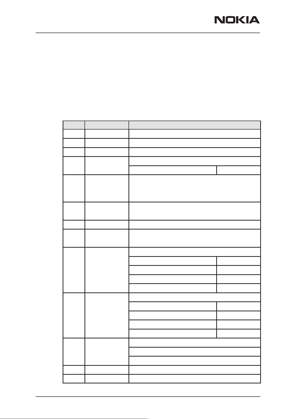
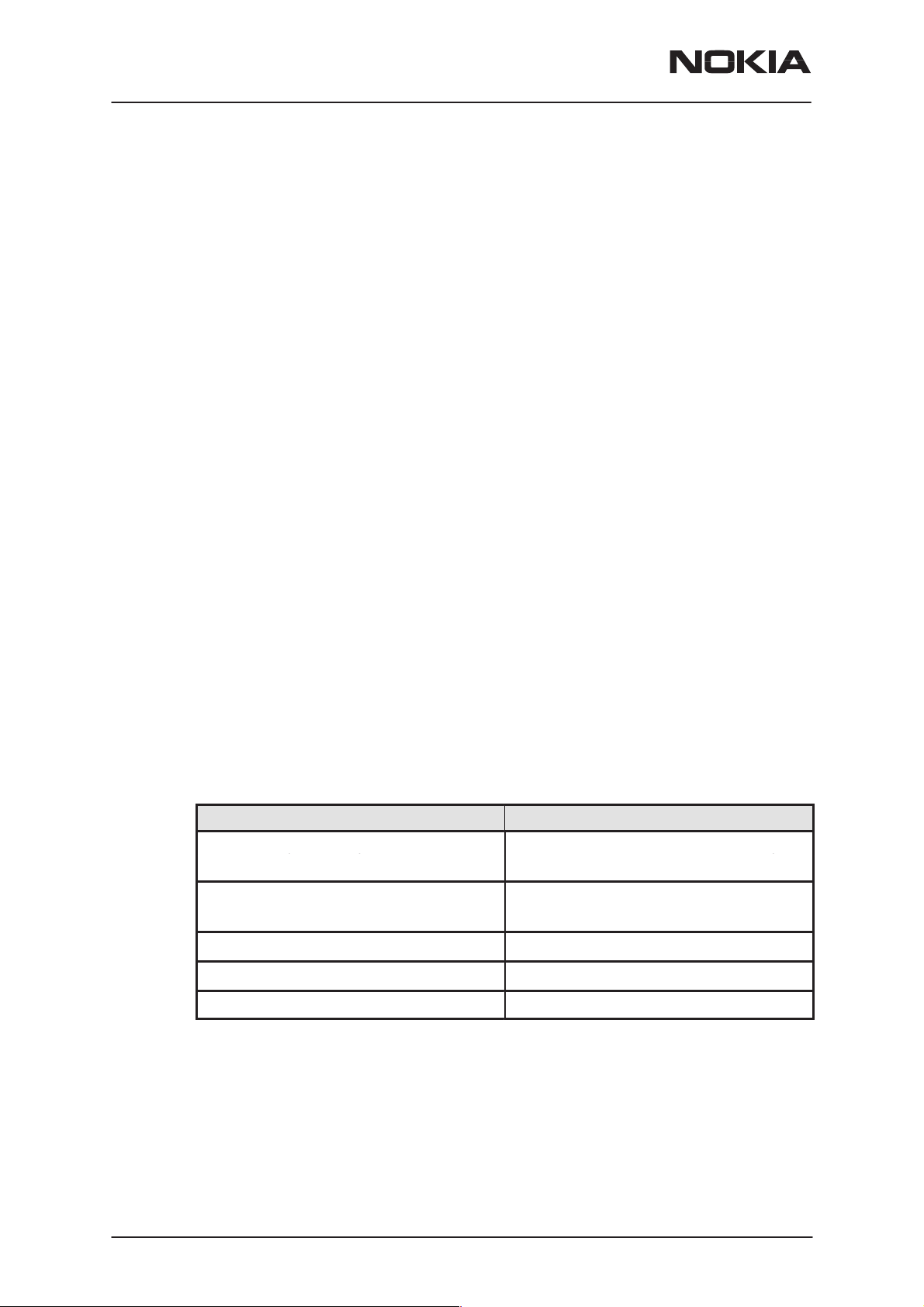
14 RFGND HF Mic ground
15 MIC_HF External HF microphone
18 XPWRON Power on/off control
NME-2A
System Module GM8
DescriptionNamePin
19 LSP Audio to HF/handset speaker
20 Shield GND Shielding
21 NC Not connected
22 NC Not connected
23 VBSW_1 Switched VBATT supply for handset
24 AGND Analog GND
25 LSPGND HF speaker ground
SIM Card Reader
• input low:
• connected to switch transistor
pulled high to VBATT
• impedance min:
• power max:
• for HS pin 1
• value:
10.8...13.2...15.6 V
0...0.2...0.7 V
3
Ω
4 W
Pin Name Description
1 GND Ground
2, 6 VSIM SIM card reader supply voltage
• voltage:
4.5...4.65...4.8 V
3 SIMDATA Data for SIM card
• state ”1”:
• state ”0”:
3.6...4.65...4.8 V
0...0.2...0.7V
4 SIMCLK Clock for SIM card
• state ”1”:
• state ”0”:
3.6...4.65...4.8 V
0...0.2...0.7 V
5 SIMRESET Reset for SIM card
• output high:
• output low:
3.6...4.65...4.8 V
0...0.2...0.7V
7 CARDDET Signal to ASIC
• card not present:
• card present:
3.6...4.65...4.8 V
0...0.2...0.7V
Issue 2 05/2000
Nokia Mobile Phones Ltd.
Page 9
Page 10
NME-2A
5
M2BUS
Serial bidirectional data and control
System Module GM8
Data Connector
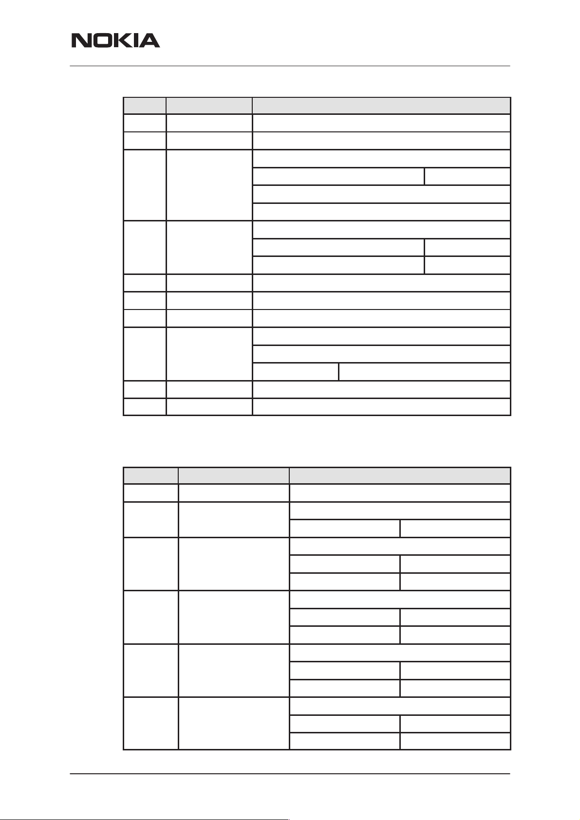
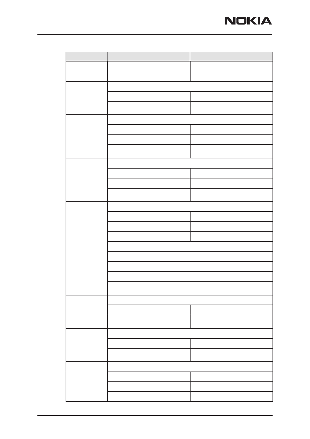
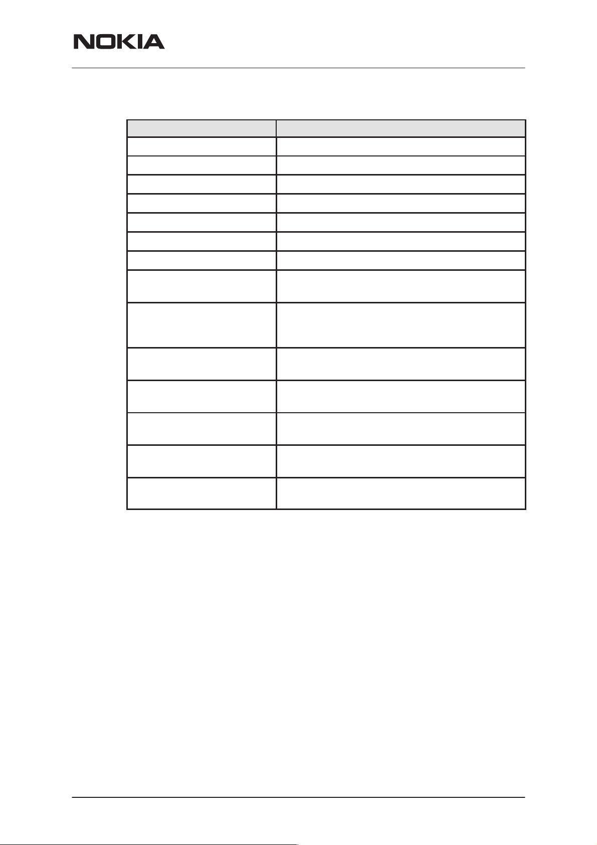
Pin Name Description
1, 9 DGND Digital ground
2 MMODE Minimum mode, input line Connect to
3 AGND Analog ground
4 TDA Transmitted DBUS data to the data card.
PAMS Technical Documentation
DGND for normal operation. Connect to
M2BUS before power–on when
flash programming.
• state ”1”:
• state ”0”:
between the phone and accessories.
6 RXD2 Flash loading data from programmer
• input low level:
• input high level:
7 TXD2 Flash acknowledge data to programmer
• output low level:
• output high level:
8, 16 NC No connection
10 NC No connection
11 DSYNC DBUS data bit sync 8 kHz clock.
• high level:
• low level:
12 RDA DBUS received data from data card.
3.6...4.65...4.8 V
0...0.2...0.7 V
0...0.2...0.7 V
3.6...4.65...4.8 V
0...0.2...0.7 V
3.6...4.65...4.8 V
3.6...4.65...4.8 V
0...0.2...0.7 V
13 NC Not used.
14 VF Programming voltage for flash.
15 DCLK DBUS data 512 kHz clock.
Page 10
• state ”1”:
• state ”0”:
• value:
• state ”1”:
• state ”0”:
Nokia Mobile Phones Ltd.
3.6...4.65...4.8 V
0...0.2...0.7 V
11.4...12...12.6 V
3.6...4.65...4.8 V
0...0.2...0.7 V
Issue 2 05/2000
Page 11
PAMS Technical Documentation
Internal Signals
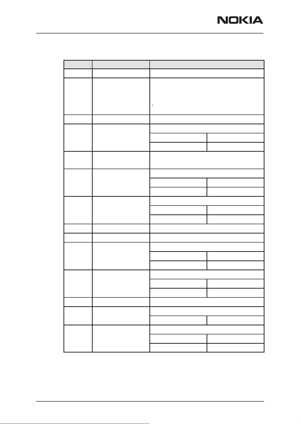
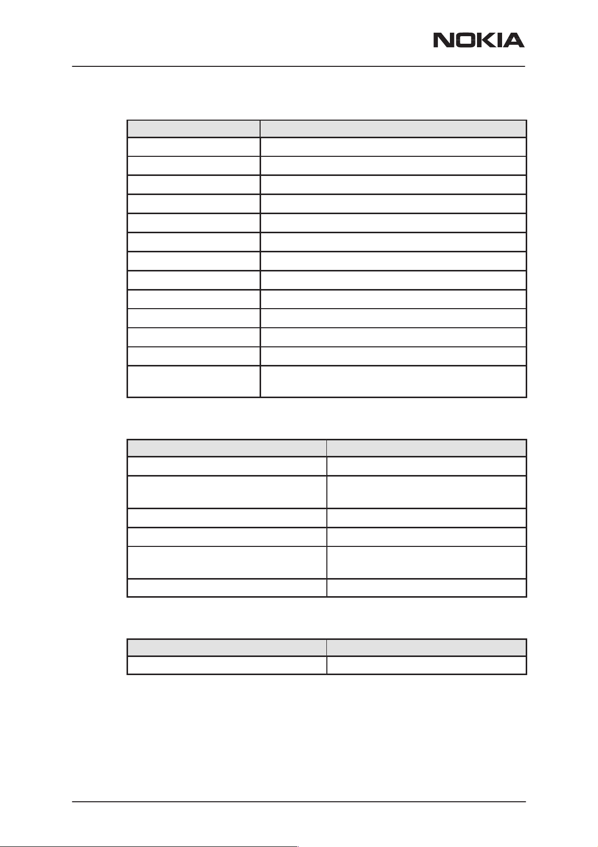
Symbol Description Values
NME-2A
System Module GM8
SCLK
SDATA
SENAR
SENAT
RXPWR
Synthesizer clock
• load impedance:
• frequency:
Synthesizer data
• load impedance:
• data rate frequency:
Synthesizer enable
• PLL contr. disabled:
• PLL activated:
• current:
Synthesizer enable
• PLL contr. disabled:
• PLL activated:
• current:
RX supply voltage on/off
10 k
Ω
3.25 MHz
10 k
Ω
3.25 MHz
4.5...4.65...4.8 V
0...0.2...0.7 V
50 µA
4.5...4.65...4.8 V
0...0.2...0.7 V
50 µA
SYNTHPWR
TXPWR
TXP
AFC
• RX supply voltage on:
• RX supply voltage off:
• current:
Supply voltage on/off
• RF regulators on:
• RF regulators off:
• current:
TX supply voltage on/off
• TX supply voltage on:
• TX supply voltage off:
• current:
TX enable
• transmitter power enable:
• transmitter power disable:
Automatic frequency control voltage
4.5...4.65...4.8 V
0...0.2...0.7 V
0.5 mA
4.5...4.65...4.8 V
0...0.2...0.7 V
1.0 mA
4.5...4.65...4.8 V
0...0.2...0.7 V
0.5 mA
4.5...4.65...4.8 V
0...0.2...0.7 V
Issue 2 05/2000
• voltage min/max:
• resolution:
Nokia Mobile Phones Ltd.
0.35...4.35 V
11 bits
Page 11
Page 12
NME-2A
System Module GM8
PAMS Technical Documentation
ValuesDescriptionSymbol
TXC
TXQP,TXQN
TXIP,TXIN
PDATA0–5
• load impedance (dynam-
10 k
ic):
TX transmit power control voltage
• voltage range min/max:
• impedance:
0.3...4.2 V
10 k
Differential TX quadrature signal
• differential voltage swing:
• d.c. level:
• load impedance:
1.15...1.2...1.25 V
2.30...2.35...2.40 V
30 k
Differential TX in phase signal
• differential voltage swing:
• d.c. level:
• load impedance:
1.15...1.2...1.25 V
2.30...2.35...2.40 V
30 k
Parallel AGC data
• reduced front end gain:
4.5...4.65...4.8 V
Ω
Ω
PP
Ω
PP
Ω
RXQ
RXI
RFC
• normal front end gain:
• current:
0...0.2...0.7 V
0.1 mA
• PDATA1; AGC 3 dB reduction
• PDATA2; AGC 6 dB reduction
• PDATA3; AGC 12 dB reduction
• PDATA4; AGC 24 dB reduction
• PDATA5; AGC 12 dB reduction
RX quadrature signal
• output level:
• source impedance:
15 mV
470
Ω
PP
RX in phase signal
• output level:
• source impedance:
15 mV
470
Ω
PP
High stability clock signal for the logic circuits
• frequency:
26 MHz
Page 12
• signal amplitude:
• load resistance:
Nokia Mobile Phones Ltd.
1.0 V
10 k
PP
Ω
Issue 2 05/2000
Page 13
PAMS Technical Documentation
NME-2A
System Module GM8
ValuesDescriptionSymbol
VREF
VBATT_RF
VBATT_I
6V5_RF
8V5_RX_TX
VAI
PA_CO
VCTCXO supply voltage
• voltage:
• current:
4.55...4.65...4.75 V
2.0 mA
Supply voltage for RF
• voltage:
10.8...13.2...15.6 V
Supply voltage for the PA module
• voltage:
10.8...13.2...15.6 V
Supply voltage for 5 V regulators
• voltage:
6.0...6.5...7.0 V
Supply voltage for BB
• voltage:
7.5...8.3...8.7 V
8.5 V regulator on/off
• logic high ”1”:
• logic low ”0”:
4.7 V
0 V
Power amplifier supply compensation
*Load Impedance
1k2 Ohm
PA_ADJ
*DC range (VBATT Supply
Switched on)
Power control loop DC–ADJ
*Voltage range
*Load Impedance
15.6–10.2 Vdc
0.3...4.6 Vdc
10k Ohm
Issue 2 05/2000
Nokia Mobile Phones Ltd.
Page 13
Page 14
NME-2A
System Module GM8
Baseband Block Description
General
The purpose of the baseband module is to control the phone, to process
audio signals to and from the RF block and to and from the handset/
handsfree transducers. The module also includes a SIM card reader and
furnishes external data and control lines.
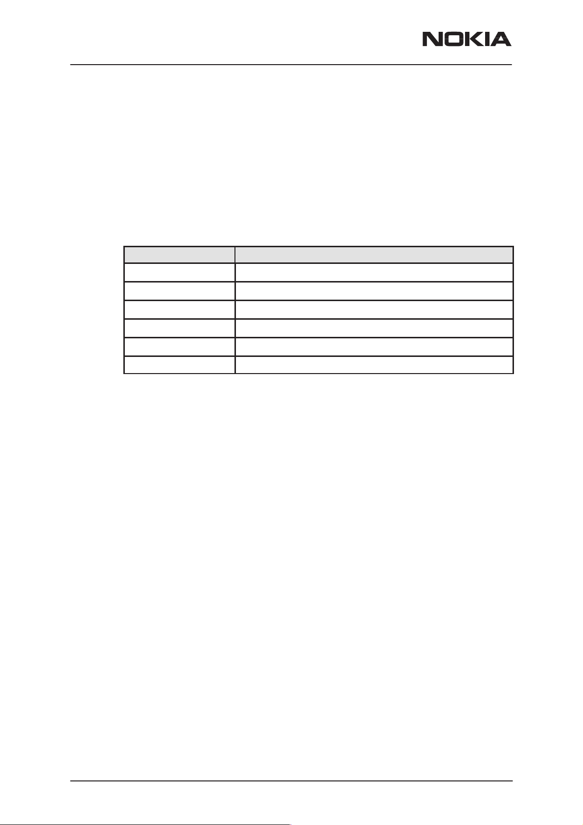
Names of Functional Blocks
Name Function
CTRLU Control unit for phone
PWRU Power supply
DSPU Digital signal processing block
PAMS Technical Documentation
AUDIO Audio coding
ASIC D2CA GSM/PCN system ASIC; several functions
RFI RF baseband interface
Page 14
Nokia Mobile Phones Ltd.
Issue 2 05/2000
Page 15
PAMS Technical Documentation
Clocking Scheme
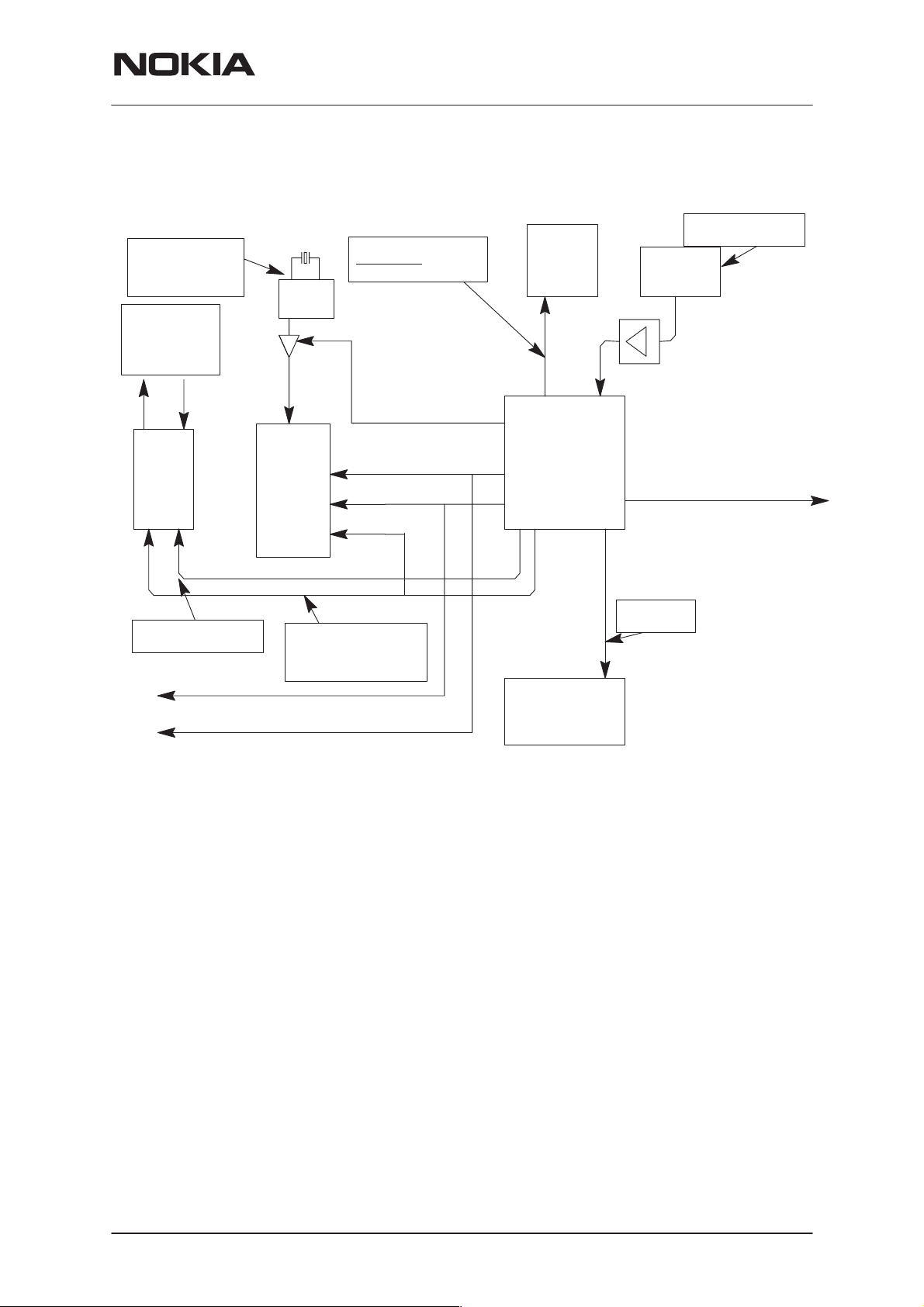
DSP Clock
60.2 MHz
differential sine
wave
HSE–6XA
ear mic
OSCILLATOR
RFI Clock 13 MHz
Sleep Mode:
135.4kHz
System Module GM8
RF System Clock
26 MHz
RFI
VCTCXO
NME-2A
AUDIO
CODEC
Codec Sync Clock
8 kHz
DBUSCLK 512kHz
DBUSSYNC 8kHz
Most of the clocks are generated from the 26 MHz VCTCXO frequency by
the ASIC:
– 26 MHz clock for the MCU. MCU‘s internal clock frequency is half of
that.
DSP
Codec Main Clock
and data Transfer
clock
512kHz
Figure 1. Clocking Scheme
ASIC
SIMCLKSIMCLK
3.25 / 1.625
MHz
MCU Clock
26 MHz
MCU
– 13 MHz for the RFI.
– The ASIC also generates 135.4 kHz sleep mode clock for the RFI
– 3.25 MHz clock for SIM. When there is no data transfer between the
SIM card and the phone the clock can be reduced to 1.625 MHz.
Some SIM cards also allows the clock to be stopped in that mode.
– 512 kHz main clock for the codec and for the data transfer between
the DSP and the codec.
– 8 kHz synchronization clock for data transfer between the DSP and
the codec.
– 512 kHz clock and 8 kHz sync. clock for the DBUS data transfer.
Issue 2 05/2000
Nokia Mobile Phones Ltd.
Page 15
Page 16
NME-2A
System Module GM8
The DSP has its own crystal oscillator. The DSP uses differential
sinusoidal clock. The frequency is 60.2 MHz. The DSP clock buffer can be
powered down via ASIC. The ASIC MCU generates 8 kHz clock to the
codec for the control data transfer.
In the idle mode all the clocks can be stopped except 26 MHz main clock
coming from the VCTCXO. The VCTCXO signal is buffered to limit
frequency pulling caused by the baseband circuits.
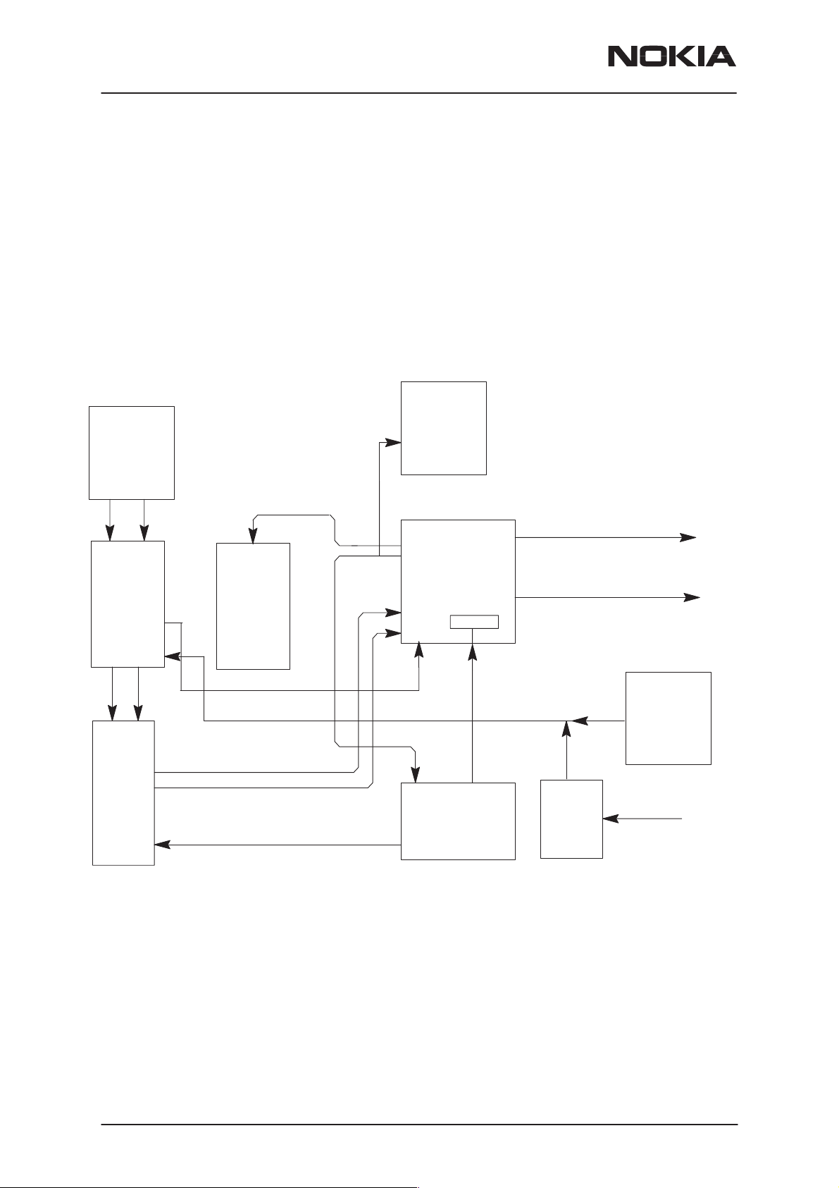
Reset and Power Control
PAMS Technical Documentation
CAR BATT
VOLTAGE
10.8––15.6
MIN / MAX
+ –
OVER/
UNDER
VOLTAGE
DETECT+
pre volt
regulator
reset in
DSP
xpwron
+–
tx off
PSL+
VL1
XRES reset in
XPwrOff
approx 2Hz
RFI
Reset Out
Reset Out
Vcc
Reset in
ASIC
resetreg
MCU
XPWRON
on/off
RF PA
SIMReset
HSE –6XA
handset
on/off
IGNS
Page 16
Figure 2. Reset & Power Control
There are two different ways to switch power on:
– Pushing the on/off button of the handset the effect of which is to
ground the input pin XPWRON of the System Connector or
– Pulling the input IGNS high.
Nokia Mobile Phones Ltd.
Issue 2 05/2000
Page 17
PAMS Technical Documentation
All devices are powered up at the same time. The PSL+ supplies the reset
to the ASIC at power up. The ASIC start delivering clock signals the to the
DSP and the MCU. After about 20 µs the ASIC releases the resets to
MCU, RFI and DSP. MCU and RFI reset is released after 256 13 MHz
clock cycles. DSP reset release time from DSP clock activation can be
selected from 0 to 255 13MHz clock cycles. In our case it is 255. SIM
reset release time is according to GSM SIM specifications.
To turn off power for the phone, the user presses the on/off key (or turns
off the ignition key of the car). The MCU detects this. The MCU cuts off
any ongoing call, exits all tasks, acts inoperative to the user and stops the
PSL+ watchdog without resets. After power–down delay, the PSL+ cuts off
the supply from all circuitry.
When the IGNS line is connected the phone will turn on when this line
goes high. The IGNS circuit pulls the XPWRON low for a approx. 200
msec as if the handset on/off button was being pushed.
NME-2A
System Module GM8
The power may be turned off by sending a turn off command on the
M2BUS from handset or through the Data Connector.
In the User Interface SW an automatic shutdown feature will be
implemented. When no activity have been observed for a user settable
period. the phone will turn off thus limiting the risk of draining the car
battery.
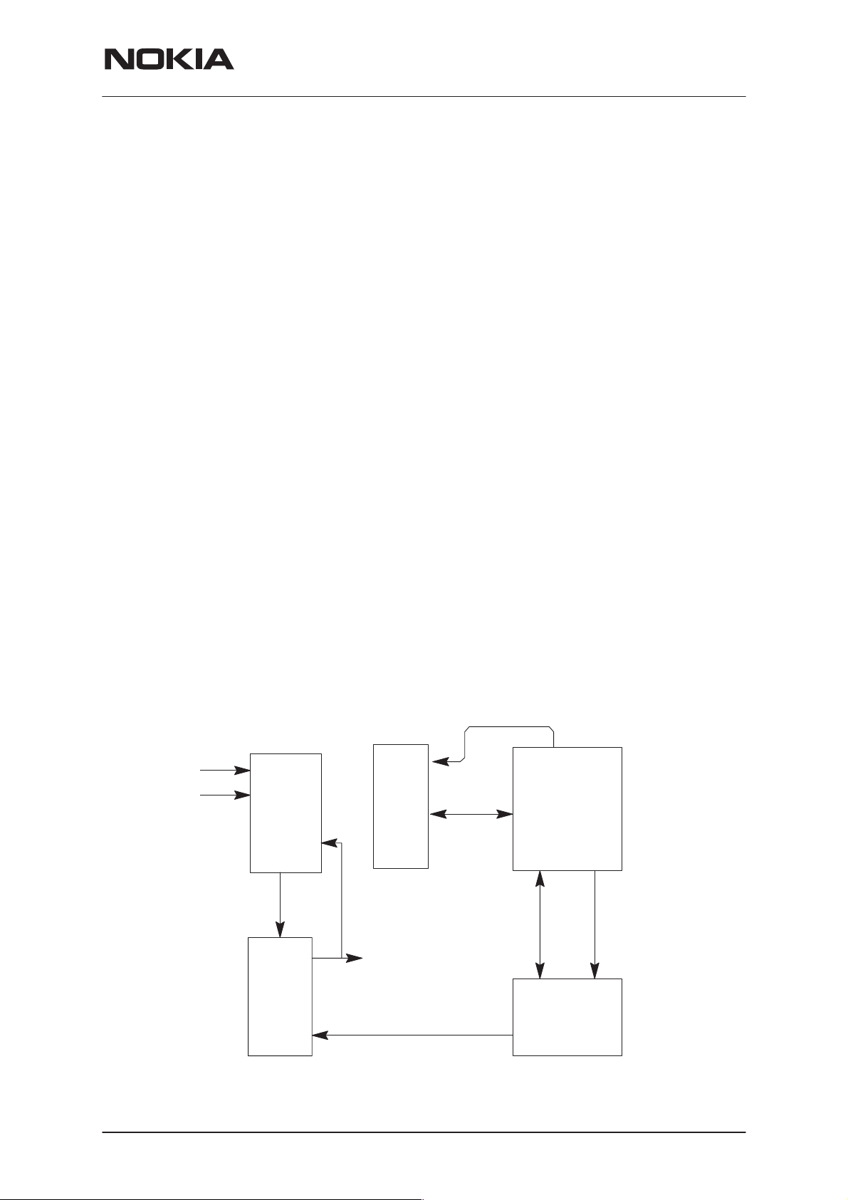
Watchdog System
VBATT
GND
PRE
REG
reset
DSP
4
1
ASIC
1
Issue 2 05/2000
PSL+
XPWROFF
5
POWER
3
2
Figure 3. Watchdog System
Nokia Mobile Phones Ltd.
4
reset
MCU
Page 17
Page 18

NME-2A
System Module GM8
Normal operation:
– 1. MCU tests DSP
– 2. MCU updates ASIC watchdog timer (> 2 Hz)
– 3. MCU pulses the XPWROFF input on the PSL+ (about 2 Hz)
Failed operation:
– 4. ASIC resets MCU and DSP after about 0.5 s failure
– 5. PSL+ switches power off about 1.5 s after the previous XPWROFF
pulse
CTRLU
The Control block contains a microcomputer unit (MCU) and three
memory circuits (FLASH, SRAM, EEPROM), a 20–bit address bus and an
8–bit data bus.
PAMS Technical Documentation
Main Features of the CTRLU Block
MCU functions:
– system control
– communication control
– handset interface functions
– authentication
– RF monitoring
– power up/down control
– self–test and production testing
– flash loading
Main Components
– Hitachi H8/536
H8/536 is a CMOS microcomputer unit (MCU) comprising a
CPU core and on–chip supporting modules with 16–bit architecture. The data bus to outside world has 8 bits.
Page 18
– 1024k*8bit FLASH memory
100 ns maximum read access time
contains the main program code for the MCU; part of the DSP
program code also located on FLASH
ASIC can address two 4 Mbit memories or one 8 Mbit memory.
– 32k*8bit SRAM memory
100 ns maximum read access time
Nokia Mobile Phones Ltd.
Issue 2 05/2000
Page 19
PAMS Technical Documentation
– 8k*8bit EEPROM memory
150 ns maximum read access time
contains user defined information
there is a register bit on the ASIC which must be set before the
write operation to the EEPROM.
Input Signals of CTRLU
Name (from) Description
VL1(PWRU) Power supply voltage for CTRLU block
VREF(PWRU) Reference voltage for MCU A/D converter
EROMSELX(ASIC) Chip select for the EEPROM memory
ROMSELX(ASIC) Chip select for the FLASH memory
ROMAD18(ASIC) Chip select for the FLASH memory (FLASH1)
NME-2A
System Module GM8
RAMSELX(ASIC) Chip select for the SRAM memory
RESETX(ASIC) Reset signal for MCU
NMI(ASIC) Non–maskable interrupt request
MCUCLK(ASIC) Main clock for MCU
IRQX(ASIC) Interrupt request
PCMCDO(AUDIO) Audio codec control data receiving
TRF(RF) RF module temperature detection
VF(data conn.) Programming voltage for FLASH memory
RXD2 The use of handsfree monitoring
(data conn.) FLASH programming data input on the produc-
tion line
MMODE Minimum mode for FLASH programming
Issue 2 05/2000
Nokia Mobile Phones Ltd.
Page 19
Page 20
NME-2A
System Module GM8
Output Signals of CTRLU
Name (from) Description
XPWROFF(PWRU) Power off control, PSL+ watchdog reset
WSTROBEX(ASIC) MCU write strobe
RSTROBEX(ASIC) MCU read strobe
MCUAD(19:0)(ASIC) 20 bit MCU address bus
MBUSDET(ASIC) MBUS activity detection
PCMCLK(AUDIO) Clock for audio cedec control data transfer
PCMCDI(AUDIO) Audio codec control data transmitting
XSELPCMC(AUDIO) Chip select for audio codec
TXD2 Verification output of the programmed
(data connector) data of FLASH during programming
PAMS Technical Documentation
Bidirectional Signals of CTRLU
Name (from) Description
MCUDA(7;0)(ASIC) MCU’s 8 bit data bus
M2BUS Asynchronous serial data bus
Block Description
– MCU – memories
The MCU has a 20 bits wide address bus A(19:0) and an 8–bit
data bus with memories. The address bits A(19:16) are used
for chip select decoding. The decoding is done in the ESA
ASIC. The ASIC can address two 4 Mbit (or smaller) or one 8
Mbit flash memories. Hitachi HD647536 processor has internal
ROM and RAM memories.
– Flash programming
In flash programming a special flash programming box and a
PC is needed. Loading is done through the 16 pole Data Connector of the mobile phone. First MCU goes to minimum mode
(MBUS command from PC or if MBUS is connected to
MMODE line during power up). Then the flash software is
loaded from PC to flash loading box. When the loading is complete, flash loading to mobile can be started by MBUS command from PC to the MCU. After that the MCU asks the test
box to start flash loading to mobile. The box supplies 12 V programming voltage for flash and starts to send 250 bytes data
blocks to the MCU via RXD2 line. The baud rate is 406 kbit/s.
The MCU calculates the check sum, sends acknowledge via
TXD2 line and sends the data to flash. When all the data are
loaded the mobile resets and tells the flash loading box if the
loading was successful or not.
Page 20
Nokia Mobile Phones Ltd.
Issue 2 05/2000
Page 21

PAMS Technical Documentation
– CTRLU – PWRU
MCU controls the watchdog timer in PSL+. It sends a positive
pulse at a rate of approximately 2 Hz to XPWROFF pin of the
PSL+ to keep the power on. If MCU fails to deliver this pulse,
the PSL+ will remove power from the system. When power off
is requested by the user or by the MCU SW, (UI SW or CS
SW), the MCU leaves the PSL+ watchdog without reset pulses.
After the watchdog time has elapsed the PSL+ cuts off the supply voltages from the phone.
– CTRLU – ASIC
MCU and ASIC have a common 8–bit data bus and a 9–bit address bus. Bits A(4:0) are used for normal addressing whereas
bits A(19:16) are decoded in ASIC to chip select inputs for
CTRLU memories. ASIC controls the main clock, main reset
and interrupts to MCU. The internal clock of MCU is half the
MCUCLK clock speed. RESETX (produced by ASIC) resets
everything in MCU except the contents of the RAM. IRQX is a
general purpose interrupt request line from ASIC. After IRQX
request the interrupt register of the ASIC is read to find out the
reason for interrupt. NMI interrupt is used only to wake up
MCU from software standby mode.
NME-2A
System Module GM8
– CTRLU – DSPU
MCU and DSP communicate through the ASIC. ASIC has an
MCU mailbox and a DSP mailbox. MCU writes data to DSP
mailbox where DSP can only read the incoming data. In MCU
mailbox the data transfer direction is the opposite. When power
is switched on the MCU loads data from the Flash memory to
the DSP‘s external program memory through this mailbox.
– CTRLU – AUDIO
When the the chip select signal XSELPCMC goes low, MCU
writes or reads control data to or from the speech codec registers at the rate defined by PCMCLK. PCMCDI is an output data
line from MCU to codec and PCMCDO is an input data line
from codec to MCU. The data and control flows on separate
serial busses.
– CTRLU – RF
MCU has internal 8 channel 10 bit AD converter. Following signals are used to monitor RF: TRF RF temperature (currently
not in use)
– CTRLU – ACCESSORIES
– MINIMUM – MODE
Issue 2 05/2000
M2BUS is used to control external accessories. This interface
can also be used for factory testing and maintenance purposes.
Nokia Mobile Phones Ltd.
Page 21
Page 22
NME-2A
()
(
System Module GM8
PWRU
The protection against overvoltage or wrong polarity on the supply lines is
included in this block which further creates the supply voltages for the
baseband block, for the RF synthesizer and switches the supply to the
handset and audio power amplifier.
Main Components
– Pre regulator
– PSL+ and ASIC
PAMS Technical Documentation
This special mode can be reached through a M2BUS command or by connecting the pin MMODE of the Data Connector
to the M2BUS while the phone is powered up.
Stabilizes the input supply voltage to 6.5 V for the PSL+and
supplies regulated power for RF module.
Generates voltages for baseband and reset signal for the
ASIC.
Contains power on switch, supply voltage detector and watchdog.
– Supply voltage monitor
Supervises the supply voltage within the specified Window.
– Power switch
Switches on the supply voltage for the pre–regulator handset
and audio power amplifier.
Input Signals of PWRU
XPWRON(handset) Power on/off button of handset (or
XPWROFF(CTRLU) Power off control, watchdog pulses
VBATT(sys.conn) Car battery voltage
8V5_RX_X(RF) Regulated voltage from RF module
Name (from) Description
IGNS sense ON signal
from MCU
IGNS(sys.conn.) Ignition sense from car ignition key
Page 22
Nokia Mobile Phones Ltd.
Issue 2 05/2000
Page 23
PAMS Technical Documentation
VBATT_RF (RF; TX+RX)
Su ly for RF regulators
Output Signals of PWRU
Name (from) Description
XRES(ASIC) Master reset
VL1(CTRLU,ASIC,RFI) Logic supply voltage
VL2(DSPU) Logic supply voltage
VA1(AUDIO,UIF) Analog supply voltage
VA2(RFI) Analog supply voltage
VREF(CTRLU,RF) Reference voltage 4.65 V ±2 %
NME-2A
System Module GM8
VBSW_I(data conn) VBATT switched for LF amplifier and for
6V5_RF Regulated supply of the baseband that sup-
VBATT_I(RF PA) Battery voltage to RF PA, fused and pro-
VBDET(ASIC) Indicates VBATT is within window allowing
IGNDET(ASIC) Indicates logic level of ignition sense input
PAOFF(RF PA) Disables RF PA when supply voltage is out-
ANTC(sys.conn) Antenna control, current limited output that
Block Description
;
pp
handset
plies power to (RF synth,TX) a part of the
RF module too
tected against overvoltage
transmission
line
side the allowed window
follows
The PSL+ IC produces the following regulated supply voltages:
In addition it has internal watchdog voltage detection. The watchdog will
cut off output voltages if it is not reset once every 1.5 (±0.75) second. The
voltage detector resets the phone if the supply voltage falls below 6.4 V .
Issue 2 05/2000
– 2 * VL 150 mA for logic
– VA1 40 mA for audios
– VA2 80 mA for RFI
– VREF 5 mA reference
Nokia Mobile Phones Ltd.
Page 23
Page 24

NME-2A
System Module GM8
The IGNS input signal from the System Connector is low pass filtered to
remove very short pulses and is then fed to a differentiation circuit which
will turn the power on by pulling XPWRON low. The filtered IGNS is also
fed to the ASIC allowing the MCU SW to monitor the actual logic state of
this pin. The IGNS turn on pulse is in the order of 200 msec.
When the phone is off no part of the circuit is powered up. The phone can
only be powered up by pushing the on/off button or pulling the IGNS line
high.
When the on/off button is pushed the power FET turns the pre–regulator
and PSL+on. The PSL+ keeps the pre–regulator on. The IGNS circuit
provides the same effect as pushing the on/off button.
The phone is turned off by pushing the on/off button. The handset transmit
an off message to the MCU which will stop emitting watchdog pulses for
the PSL+. The PSL+ times out and the phone turns off.
PAMS Technical Documentation
DSPU
Main interfaces of the DSP:
– MCU via ASIC mailbox
– ASIC
– audio codec
– data bus interface (DBUS) for accessories
– digital audio interface (DAI) for type approval measurements
Main features of the DSP block:
– speech processing
– speech coding/decoding
– RPE–LTP–LPC (Regular pulse excitation long
term prediction linear predictive coding)
– voice activity detection (VAD) for discontinuous transmis-
sion (DTX)
– comfort noise generation during silence
Page 24
– acoustic echo cancellation
– channel coding and transmission
– block coding (with ASIC)
– convolutional coding
– interleaving
– ciphering (with ASIC)
– burst building and writing it to ASIC
Nokia Mobile Phones Ltd.
Issue 2 05/2000
Page 25

PAMS Technical Documentation
– Reception
– reading the A/D conversion results from ASIC
– impulse response calculation
– matched filtering
– bit detection (with Viterbi on ASIC)
– de–interleaving of soft decisions
– convolutional decoding (with Viterbi)
– block decoding (with ASIC)
– Adjacent cell monitoring
– signal strength measurements
– neighbor timing measurements
– neighbor parameter reception
NME-2A
System Module GM8
– control functions
– RF controls
– frame structure control
(with ASIC)
– test functions
– functions for RF measurements
– debugging functions for product development
– synthesizer control
– power ramp programming
– automatic gain control (AGC)
– automatic frequency control (AFC)
– controlling the operations during a TDMA frame
– controlling the multi–frame structure
– channel configuration control
Main Components of DSPU
– AT&T DSP 1616–X11
Digital signal processor with 12 kword internal ROM
– Two 32k *8 70 ns SRAMs for DSP external memory
– 60.2 MHz crystal oscillator to generate differential small signal clock
for the DSP
Issue 2 05/2000
Nokia Mobile Phones Ltd.
Page 25
Page 26
NME-2A
System Module GM8
Input Signals of DSPU
Name (from) Description
VL1(PWRU) Logic supply voltage for DSP clock and buffer
VL2(PWRU) Logic supply voltage
DSPCLKEN(ASIC) Clock enable for DSP clock oscillator circuit
DSP1RSTX(ASIC) Reset for the DSP
PCMDATRCLKX PCM data input clock,
(ASIC) DBUS data output clock
CODEC_CLK PCM data output clock
PCMOUT(AUDIO) Received audio in PCM format
DBUSCLK DBUS data output clock
DBUSSYNC DBUS data bit sync clock
PAMS Technical Documentation
RDA(data conn.) DBUS received data
INT0, INT1(ASIC) Interrupts for the DSP
PCMCOSYCLKX
(ASIC)
Output Signals of DSPU
Name (from) Description
PCMIN(AUDIO) Transmitted audio in PCM format
IOX(ASIC) I/O enable, indicates access to
RWX(ASIC) Read/write X
DSPAD(16;9)(ASIC) Address bus and control signals
DBUSDET(ASIC) RDA line for DBUS activity detec-
TDA(data conn.) DBUS transmitted data
Bidirectional Signals of DSPU
PCM data bit sync clock
DSP address space
tion by ASIC
Page 26
Name (from) Description
DSPDA(15;0)(ASIC) 16 bit data bus
Nokia Mobile Phones Ltd.
Issue 2 05/2000
Page 27

PAMS Technical Documentation
Block Description of DSPU
The Control unit communicates with the DSP circuitry through a mailbox in
the ESA ASIC. The part of the DSP SW that resides in external SRAM is
loaded from Flash Prom is software is loaded through this mailbox at start
up.
The DSP includes two serial busses. One is used for speech data transfer
between the DSP and the codec. The other is used as an external data
bus and it is connected to the Data Connector. This bus can be used by
data accessories and also as a digital audio interface (DAI) in audio type
approval measurements. The clocks (512 kHz main clock and 8 kHz sync.
clock) are generated by the ASIC.
In transmit mode the DSP codes the speech and routes the resulting
transmit slots to the ESA. The ESA ASIC controls timing, and at specified
intervals sends these bits to the RFI for DA conversion.
NME-2A
System Module GM8
AUDIO
In digital receive mode the RFI AD converts the IF signal from the RF unit
under the control of the ESA. The DSP controls the ESA and receives the
converted bits. After channel and speech decoding, bits are converted into
an analog signal in the PCM codec, routed and fed to the earpiece/
loudspeaker.
The DSP controls the RF module through the ESA ASIC, where all
necessary timing functions are implemented, and control I/O lines are
provided eg. for synthesizer loading.
The DSP emulator can be connected to DSP pins TCK, TMS, TDO, TDI,
GND and VDD.
The DSP clock buffer can be turned off via a control pin on the ASIC to
save current when the DSP clock is not needed.
The AUDIO block consists of an audio codec , conditioning amplifiers for
the audio inputs and outputs and a power amplifier for the external
loudspeaker.
The codec contains microphone and earpiece amplifiers and all the
necessary switches for signal routing. The codec is controlled by the
MCU. The PCM data comes from and goes to the DSP.
The power amplifier drives the external loudspeaker for handsfree
function, and a highpass filter removes unwanted low frequency noise
picked up by the handsfree microphone.
Issue 2 05/2000
Nokia Mobile Phones Ltd.
Page 27
Page 28
NME-2A
PCMIN(DSPU)
Received audio in PCM format
System Module GM8
Main Components of AUDIO
– Class B amplifier built using an op amp and discrete power transistors.
– Audio codec ST5080
– Contains: PCM codec, audio routing switches, microphone and ear-
piece amplifiers for 2 connections (internal and external devices) and
DTMF generator.
High pass filter/amplifier for the handsfree microphone.
Power amplifier for the external handsfree loudspeaker.
Input Signals of AUDIO
Name (from) Description
VA1(PWRU) Analog supply voltage
VBSW_1(PWRU) Switched VBATT supply for the
PAMS Technical Documentation
pre–regulator power amplifier (and
handset)
SYNC(ASIC) 8 kHz frame sync
CODEC_CLK(ASIC) 512 kHz codec main clock
PCMCDI(CTRLU) Audio codec control data
PCMCLK(CTRLU) Clock for audio codec control data
XSELPCMC (CTRLU) Audio codec chip select
HFMIC(syst.conn.) External microphone
NOK_OEM(ASIC)
MIC(syst.conn) Handset microphone
Output Signals of AUDIO
Name (to) Description
PCMOUT(DSPU) Transmitted audio in PCM format
PCMCDO(CTRLU) Audio codec control data
transfer
Control line to set the mic sensitivity according to
VDA recommendations
EAR(syst.conn.) Audio to handset
LSP(syst.conn) Audio to handsfree loudspeaker
Page 28
Nokia Mobile Phones Ltd.
Issue 2 05/2000
Page 29

PAMS Technical Documentation
Block Description of AUDIO
The handset microphone is connected to the codec through an attenuator.
The external handsfree microphone is DC–biased by approx. 8V. The
handsfree mic signal is amplified and filtered and fed to the codec.
The gain of the ext. microphone input can be selected to one of two
settings, one adjusted for the standard Nokia microphone and a less
sensitive one adjusted for the VDA recommended sensitivity.
The microphone signal is A/D converted in thee PCM codec (A–law) and
delivered to the DSP.
Digital downlink signal from the DSP is fed to the D/A converter of the
codec. After the conversion the signal is low pass filtered and fed to a
attenuator operating as volume control and routing switches to direct it to
the earpiece of the handset or the power amplifier for the loudspeaker.
NME-2A
System Module GM8
ASIC
There are 8 separate volume settings. They cover a range of 15 dB for the
earpiece and a range of 31 dB for the handsfree speaker.
The audio codec communicates with the DSP (analog speech) through an
SIO (signals: PCMIN, SYNC, CODEC_CLK and PCMOUT) . The MCU
controls the audio codec function through a separate serial bus (signals:
PCMCDO, PCMCDI, PCMCLK and XSELPCMC). Gainsetting, routing ,
tone generation etc in the codec is controlled through writing to registers
in the codec. The 512 kHz clock and 8 kHz sync signal are produced by
the ASIC clock signals.
The codec generates DTMF tones (key beeps), ringing and warning tones
etc. for the external speaker. Some tones come also from the network.
The ASIC takes care of the following functions :
– interface between MCU, DSP and RFI
– hardware accelerator functions to DSP SW
– clock generation, clock distribution and clock disable/enable
– RF controls
– Timers
– M2BUS and D–BUS detect and D–BUS clock and sync generation
– SIM interface
– Control inputs and outputs for the system connector.
Main Components of ASIC
– ESA ASIC
– RFC buffer, a package of logic level inverters
Issue 2 05/2000
Nokia Mobile Phones Ltd.
Page 29
Page 30
NME-2A
System Module GM8
Input Signals of ASIC
Name (from) Description
VL1(PWRU) Logic supply voltage
VL2(PWRU) Logic supply for SIM reader
IOX(DSPU) I/O enable, indicates access to DSP address
RWX(DSPU) Read/write X
WSTROBEX (CTRLU) MCU’s write strobe
RSTROBEX (CTRLU) MCU’s read strobe
RFC(RF) Reference clock from VCTCXO
XRES(PWRU) Master reset
DSPAD(16;0)(DSPU) Address bus and control signals
PAMS Technical Documentation
space
MCUAD(19;16,4;0)
(CTRLU)
DAX(RFI) Data acknowledge
MBUSDET(CTRLU) MBUS activity detection
DBUSDET(DSPU) DBUS activity detection
IGNDET(PWRU) Logic level of IGNS
VBDET(PWRU) Indicating VBATT is within window to allow
SIM_DETECT Logic signal indicating that a SIM card is pres-
PAOFF(PWRU) Indicating that operation of the RF PA stage is
Output Signals of ASIC
Name (to) Description
INT0,INT1(DSPU) Interrupts for DSP
NMI(CTRLU) Not maskable interrupt request
MCU’s address bus
transmission
ent (SIM reader)
disabled
Page 30
IRQX(CTRLU) Interrupt request
RESETX (CTRLU,RFI) Master (power up) reset
DSP1RSTX(DSPU) Reset for the DSP
WRX(RFI) Write strobe
RDX(RFI) Read strobe
RFIAD(3;0)(RFI) RFI address bus
SCLK(RF) Synthesizer load clock
SDATA(RF) Synthesizer load data
Nokia Mobile Phones Ltd.
Issue 2 05/2000
Page 31

PAMS Technical Documentation
SENAR(RF) Receiver synthesizer enable
SENAT(RF) Transmit synthesizer enable
RXPWR(RF) RX circuitry power enable
TXPWR(RF) TX circuitry power enable
SYNTHPWR(RF) Synthesizer circuitry power enable
TXP(RF) Transmit enable
MCUCLK(CTRLU) Main clock for MCU
DSPCLKEN(DSPU) DSP clock circuit enable
RFICLK(RFI) RFI master clock
RFI2CLK(RFI) RFI sleep clock
NME-2A
System Module GM8
DescriptionName (to)
CODEC_CLK (DSPU,AU-
PCM data clock
DIO)
PCMDATRCLKX Inverted PCM data clock, used as input
clock for
(DSPU) codec and DBUS interface
SYNC(AUDIO) Bit sync clock
PCMCOSYCLKX (DSPU) Bit sync clock, inverted
DCLK(DSPU) DBUS data clock
DSYNC(DSPU) DBUS bit sync clock
SIMCLK(UIF) SIM data clock
VSIM(UIF) SIM power control
ROMSELX(CTRLU) Chip select for the FLASH memory
ROMAD18 (CTRLU) Chip select for the FLASH memory
(FLASH1)
EROMSELX (CTRLU) Chip select for the EEPROM memory
RAMSELX(CTRLU) Chip select for the SRAM memory
CRM(sys.conn) Car radio mute
NOKIA_OEM (AUDIO) Set ext. mic. sensitivity to VDA recom-
PA_ADJ Power adjustment for RF PA.
EAL(sys.conn) External alert
Issue 2 05/2000
mended value
Nokia Mobile Phones Ltd.
Page 31
Page 32

NME-2A
System Module GM8
Bidirectional Signals of ASIC
Name (from) Description
DSPDA(15;0)(DSPU) 16 bit data bus
MCUDA(7;0)(CTRLU) MCU’s 8 bit data bus
RFIDA(11;0)(RFI) 12 bit data bus
SIMDATA(UIF) Serial data to SIM
Block Description of ASIC
PSL+ supplies the reset to the ASIC at power up. The ASIC starts the
clocks to the DSP and the MCU. After about 20 µS the ASIC releases the
resets to all circuitry. MCU and RFI reset is released after 256 13 MHz
clock cycles. DSP reset release time from DSP clock activation can be
selected from 0 to 255 13 MHz clock cycles. In our case 255 is selected.
SIM reset release time is according to GSM SIM specifications.
PAMS Technical Documentation
Two inverters buffers the 26MHz clock from the VCTCXO to the ASIC to
minimize the effect on the clock signal caused by varying load on the
clock. In the ASIC the clock is further buffered, divided and gated for the
MCU, RFI, SIM. The ASIC. It also generates main and sync clocks for
audio codec, DSP‘s SIOs and DBUS. The clock outputs can be disabled in
order to save current when the clock is not needed. The DSP oscillator
buffer can be turned off by the ASIC.
Interface to the MCU consists of 8 bit data bus ,5 bit lower address bus, 4
bit upper address bus, RSTRBEX, WSTROBEX, IRQX and NMI. ASIC is
in the same memory space as MCU memories (memory mapped on the
MCU). The ASIC generates chip select’s from the address bits A16–19.
There is also M2BUS detector, netfree counter and D–BUS detector in the
ASIC. Netfree interrupt IRQX occurs if no activity is detected in M2BUS in
about 3 ms. NMI is used to wake up the MCU from sleep mode.
MCU and DSP communicate through ASIC. ASIC has an MCU mailbox
and a DSP mailbox. MCU writes data to DSP mailbox where DSP can only
read the incoming data. In MCU mailbox the data transfer direction is the
opposite. The size of the mailbox is 64 * 8 bit.
The SIM interface is the electrical interface between the smart card used
in the GSM and the MCU via the ASIC. ASIC converts the serial data
received from the SIM to parallel data for MCU and converts parallel data
from MCU to serial mode for the card. The SIM interface also takes care
of the power up and down procedure to the card, frame and parity error
checking. The communication between card and ASIC is asynchronous
and half duplex. Four signals are used between the ASIC and the SIM
card: SIMDATA, SIMCLK,SIMRESET and VSIM. The clock frequency is
3.25 MHz. When there is no data transfer between the SIM card and the
Page 32
Nokia Mobile Phones Ltd.
Issue 2 05/2000
Page 33

PAMS Technical Documentation
Mobile the clock can be reduced to 1.625 MHz. Some SIM cards also
allows the clock to be stopped in that mode. Supply voltage VSIM can be
switched off by the ASIC. The supply voltage is 4.65 V. The carddetect
input on the ASIC is connected to the carddetect switch of the SIM reader
and when the pin goes low (card not present) the ASIC will drive the SIM
Interface down in a controlled and well specified manner. The carddetect
switch is activated by the SIM–card and wil open/close while the contacts
of the SIM card are engaged with the SIM reader.
The interface to the DSP consists of 6 bit address bus, 16 bit data bus,
IOX and RWX lines. Data bus is latched using IOX, address bus is not.
The ASIC also generates interrupt INT0 when an edge occurs in DBUS
line (if the mask bit is off). INT1 is used as RX interrupt and as MFI
modulator interrupt to the DSP.
The Viterbi block is used to perform GSM/PCN convolutional decoding
and bit detection according to viterbi algorithm. It can be controlled and
accessed thoroughly by the DSP.
NME-2A
System Module GM8
RFI
Coder is used to perform block encoding, decoding, and ciphering
according to GSM algorithm A5 (only A5 not A5–2).
The ASIC takes care of the interface between the DSP and the RFI: TX
modulator, RX filter, TX and RX sample buffers and controlling state
machine. The interface to RFI consists 12 bit data bus, 4 bit address bus,
RDX and WRX. There is data acknowledge (DAX) from RFI to ASIC. Also
in this block are the serial RF synthesizer interface (SCLK, SDAT) and the
digital RF control signals (RXPWR, TXPWR, TXP, SYNTHPWR)
The RFI block consists of the RFI ASIC and its reference voltage
generator. This block is an interface between the RF and baseband
sections. The RFI block has the following functions:
– Receive and A/D convert the II and Q signals delivered by the IF am-
plifier of the RF module
– Produce I and Q TX modulation signals through D/A conversion plus
filtering
– Prepare the Automatic Frequency Control signal via D/A conversion
– Prepare TX power ramp TXC via D/A conversion
– Hold AGC setting data in a register
Main Components of RFI
– RFI ASIC
– 4.096 V external voltage reference LM4040 for RFI
Issue 2 05/2000
Nokia Mobile Phones Ltd.
Page 33
Page 34

NME-2A
System Module GM8
Input Signals of RFI
VL1(PWRU) Logic supply voltage
VA2(PWRU) Analog supply voltage
RESETX(PWRU) Master (power up) reset
RFIAD(3;0)(ASIC) RFI address bus
RDX(ASIC) Read strobe
WRX(ASIC) Write strobe
RFICLK(ASIC) RFI master clock
RFI2CLK(ASIC) RFI sleep clock
RXQ(RF) RX quadrature signal
PAMS Technical Documentation
Name (from) Description
RXI(RF) RX in phase signal
Output Signals of RFI
Name (to) Description
DAX(ASIC) Data acknowledge
AFC(RF) Automatic frequency control voltage
TXC(RF) TX transmit power control voltage
TXQP,TXQN(RF) Differential TX quadrature signal
TXIP,TXIN(RF) Differential TX in phase signal
PDATA(5;0)(RF) Parallel AGC data for controlling the RF
VREF_2(PWRU) Reference used by VBATT window compa-
Bidirectional Signals of RFI
Name (to) Description
RFIDA(11;0)(ASIC) 12 bit data bus
AGC amplifiers
rator
Block Description of RFI
The RFI provides A/D conversion of the in–phase (RXI) and quadrature
(RXQ) signals in the receive path. It has got 12 bit sigma–delta A/D
converters and the sample rate is 541.667 kHz.
Analog transmit path includes 8 bit D/A converters to generate the
in–phase (TXI) and quadrature (TXQ) signals. RFI has differential outputs
for TXI and TXQ. The sample rate is 1.0833 MHz.
Page 34
Nokia Mobile Phones Ltd.
Issue 2 05/2000
Page 35

PAMS Technical Documentation
There is a 11 bit D/A converter for automatic frequency correction. The
sample rate is 1.3542 kHz.
Power ramp is done with 10 bit D/A converter. The sample frequency is
1.0833 MHz.
Digital AGC control is done with PDATA outputs.
The RFI has 12 bit data bus to the ASIC. The registers in the RFI are
accessed using 4 address bits. Control and clock signals are produced by
the ASIC.
The RFI has external 4.096 V voltage reference.
NME-2A
System Module GM8
Issue 2 05/2000
Nokia Mobile Phones Ltd.
Page 35
Page 36

NME-2A
System Module GM8
RF Block Description
The RF block carries out all the RF functions of the transceiver. The RF
block works in GSM system.
Regulators
There are three regulators in the RF unit. The 1’st regulator is used for the
synthesizers. The 2’nd regulator is used for the receiver and the
transmitter discrete circuits. The 3’rd regulator (8.3V) is used for the TX
ramping circuit and RX amplifiers. The regulators reduce the car supply
voltage to the fixed 5.0 V and 8.3 V. The receiver, synthesizer and
transmitter circuits can be switched ON and OFF separately. Switching
sequence timing depends on the operation mode of the phone.
Power Distribution
PAMS Technical Documentation
All currents in the power distribution diagram (see RF Power Distribution
Diagram) are values with the sub modules in ”on” condition. Activity
percentages in SPEECH mode are 22.5 % for RXPWR, 15.8 % for
TXPWR and 100 % for SYNTHPWR. In IDLE mode, activities are 0.36 %,
0.0 % and 1.61 %, respectively. Switching of the supply voltage for each
block is controlled independently, and for example TXPWR and RXPWR
are not on, at the same time.
Current Consumption
In the following table the RF current consumption can be seen with
different status of the control signals. The VCTCXO is not included in the
results.
SYNTHP
WR:
L L L L 0.1 mA Leakage current
H L L L 45 mA Synthesizers and
H H L L 60 mA Receive mode
H L H H 4500 mA Transmission
RXPWR: TXPWR: TXP: Typ load
Notes:
current:
VCTCXO active
Page 36
Nokia Mobile Phones Ltd.
Issue 2 05/2000
Page 37

PAMS Technical Documentation
Receiver
The received RF signal from the antenna is fed via a duplex filter to the
receiver unit. The duplex filters receiver branch is a bandpass filter. The
signal is amplified by a discrete low noise preamplifier. The gain of the
amplifier is controlled by the AGC control line (PDATA0). The nominal gain
of 15 dB is reduced in strong field conditions by about 30 dB. After the
preamplifier the signal is filtered by a dielectric filter. The filter and the
duplex filter rejects outband spurious signals coming from the antenna
and spurious emissions coming from inside the receiver unit. After the
filter a second LNA is placed in order to have enough gain before the
mixer.
The received signal is down converted by a passive double balanced
mixer. The first IF is 71 MHz.
The IF–signal is filtered using a SAW filter. This filter reject adjacent
channels signal, intermodulation signals and the second mirror. The AGC
dynamic range is split up in two amplifiers. First AGC–amplifier with
maximum 45 dB, and second AGC–amplifier with maximum 12 dB gain.
Last mentioned amplifier is integrated in the receiver IC. The 57 dB gain is
regulated in 3 dB step, using AGC control line PDATA 1–4. The second IF
center frequency is 13 MHz. The second IF mixer is integrated in the
receiver IC. The 13 MHz filter is a cheap ceramic filter. Also this filter has
adjacent channel and intermodulations rejection. Before the 13 MHz IF
signal is A/D–converted, the signal is amplified and split up in two
quadrature signals, using high and low pass filters.
NME-2A
System Module GM8
Duplex Filter
The duplex filter consists of two filters, RX and TX filter branch. The TX
filter is a notch–filter and it rejects the noise power at the RX frequency
band and TX harmonic signals. The RX filter (bandpass) rejects outband
blocking and spurious signals coming from the antenna.
Center frequency:
Pass band width (BW): ±
Insertion loss at BW:
Ripple at BW:
Terminating impedance:
V.S.W.R. at BW:
TX attenuation:
• 935...960 MHz
• 1780...1830 MHz
• 2670...2745 MHz
Parameter Value TX Value RX
902.5 Mhz 947.5 MHz
12.5 MHz
±
12.5 MHz
1.5 dB max. 2.6 dB max.
1.2 dB max. 1.5 dB max.
50
Ω
50
Ω
1.8 max. 1.8 max.
30 dB min.
30 dB min.
30 dB min.
Issue 2 05/2000
Nokia Mobile Phones Ltd.
Page 37
Page 38

NME-2A
2805
2880 MH
System Module GM8
RX attenuation:
PAMS Technical Documentation
Value RXValue TXParameter
• D.C...915 MHz
• 980...1031 MHz
• 1870...1920 MHz
•
Permissible input power:
Pre–Amplifier
The pre–amplifier amplifies the received signal coming from the antenna.
Frequency band:
Supply voltage (min/max):
Current consumption (max):
Insertion gain (min/typ):
Gain flatness: ±
Noise figure (max):
Reverse isolation (min):
...
35 dB min.
23 dB min.
30 dB min.
z
15 dB min.
8.0 W (avg)
Parameter Value
935...960 Mhz
7.65...9.35 V
10 mA
14.5...15 dB
0.5 dB
2.0 dB
15 dB
Gain reduction PDATA0=1 (typ):
IIP3: (min/typ):
Input VSWR; Zo=50 Ω (max):
Output VSWR; Zo=50 Ω (max):
RX Interstage Filters
The RX interstage filter is a dielectric filter. The filter rejects the outband
spurious and blocking signals coming from the antenna.
Terminating impedance:
Operation temperature range:
Center frequency:
Bandwidth (BW): ±
Insertion loss in BW (max):
Ripple at BW:
V.S.W.R. at BW:
35 dB
0 dBm
2.0
2.0
Parameter Value
50
Ω
–25...+85°C
947.5 MHz
12.5 MHz
2.0 dB
1.0 dB
1.8
Page 38
Attenuation
• D.C...890 MHz (min/max):
Nokia Mobile Phones Ltd.
30...15 dB
Issue 2 05/2000
Page 39

PAMS Technical Documentation
NME-2A
System Module GM8
ValueParameter
• 890...915 MHz (min/max):
• 980...1031 MHz (min/max):
• 1077...1102 MHz (min/max):
• 1870...1920 MHz (min/max):
• 1941...2062 MHz (min/max):
• 3015...3093 MHz (min/max):
Second LNA
This LAN adds gain before the mixer.
Frequency band :
Supply Voltage (min/max):
Current consumption (max) :
Insertion gain (typ)
Gain Flatness:
Noise figure (max):
12...15 dB
12...15 dB
40...50 dB
30...50 dB
30...48 dB
3.0...12 dB
Parameter Value
935...960 Mhz
7.65...9.35V
14mA
8dB
+/– 0.5dB
2.8dB
First Mixer
IIP3 (typ):
Input VSWR; Zo=50 (max)
Output VSWR; Zo=50 (max)
13dBm
2.0
2.0
The first mixer is a passive single balanced mixer. The mixer down
converts the received RF signal to the 1st IF signal, 71 MHz.
Parameter Value
RX frequency range (min/max):
LO frequency range (min/max):
IF range (typ):
Input intercept point, IIP3
LO power level (min):
Noise figure (typ):
Conversion gain (typ):
935...960 Mhz
1006...1031 Mhz
71 Mhz
+10 dBm
3 dBm
7 dB, SSB
–7 dB
Issue 2 05/2000
Nokia Mobile Phones Ltd.
Page 39
Page 40

NME-2A
System Module GM8
First IF Amplifier
The first IF amplifier is based on discrete components. It compensates for
missing amplification in the frontend.
PAMS Technical Documentation
Parameter Value
Supply voltage (min/typ/max):
Current consumption (typ/max):
Frequency range:
Conversion gain (typ):
Noise figure (typ):
Input intercept point (typ):
Input compression point (typ):
Parameter
In/out matching (typ):
First IF Filter
The channel selectivity of the receiver is split up in first and second IF
filters. The 71 MHz filter is a low loss SAW filter from Siemens. The filter
has single–ended input and balanced output.
Center frequency:
8.5 V
20 mA
71 Mhz
16 dB
3 dB
+3 dBm
0 dBm
Value
50
Ω
Parameter Value
71 MHz
Operation temperature range:
Input impedance:
Output impedance:
Insertion loss (nom/max):
Group delay distortion (nom/max):
2 dB bandwidth (min): ±
3 dB bandwidth (min): ±
±200 kHz (min):
±400 kHz (min):
±600 kHz (min):
±800 kHz (min):
±1600 kHz (min):
Spurious rejection at fo–26 MHz:
–20...+80 °C
3.5 kΩ//6.9 pF balanced
3.4 kΩ//6.7 pF balanced
11.5...13.5 dB
700...1300 ns
80 kHz
120 kHz
0 dB
23 dB
36 dB
40 dB
42 dB
60 dB
Page 40
Nokia Mobile Phones Ltd.
Issue 2 05/2000
Page 41

PAMS Technical Documentation
AGC Amplifier
The total dynamic AGC range for the receiver is 93 dB. The AGC amplifier
from AT&T has 0...45 dB AGC gain. The gain step is adjusted in 3 dB
step, using the interface lines data[1]–data[5].
Parameter Value
NME-2A
System Module GM8
Supply voltage (min/max):
Current consumption (max):
Frequency range (min/max):
Amplifier gain (nom):
Parameter Value
Amplifier gain control range (min/
max):
AGC step size:
Noise figure:
Output intercept point (max):
Absolute gain inaccuracy (max): ±
Relative gain inaccuracy (max): ±
4.5...5.5 V
16 mA
4...100 MHz, 3 dB cutoff
45 dB
0...45 dB
3 dB
10 dB
10 dB
0.5 dB over temp, range
0.3 dB
Receiver IF IC
The receiver integrated circuit is a semi–custom bipolar IC PMB2403
V1.4. The IC consist of the second IF mixer, 12 dB AGC amplifier and two
dividers.
Supply voltage (min/max):
Supply current (max):
Input frequency range (min/max):
Local freq. range of mixer (min/
max):
Conversion gain (nom):
Output compression point (min):
AGC gain step (min/max):
Absolute gain inaccuracy (max): ±
AGC Amplifier + 2nd Mixer Value
4.5...5.5 V
31 mA
45...100 MHz
170...400 MHz
12 dB
0.4 V
PP
0...12 dB
0.5 dB over temp. range
Issue 2 05/2000
Nokia Mobile Phones Ltd.
Page 41
Page 42

NME-2A
System Module GM8
PAMS Technical Documentation
Dividers Value
Input frequency range (min/max):
Divider ratio (nom):
Input power level (nom):
Output power level (min):
Second IF Filter
The second IF is a ceramic filter. This filter is inserted to obtain channel
selectivity in the receiver.
Terminating impedance (nom):
Operating temp. range (min/max):
Center frequency:
1 dB bandwidth (min): ±
5 dB bandwidth (max): ±
Insertion loss (max):
Group delay distortion (max):
180...400 MHz
1/2/4
–10 dBm
–5 dBm
Parameter Value
330
Ω
–30...+85 °C
13 MHz
90 kHz
220 kHz
6 dB
1500 ns at BW
Parameter
Attenuation
• fo ±400 kHz (min/nom):
• fo ±600 kHz (min/nom):
Second IF Amplifier
The second IF amplifier compensates for losses in the gain compensating
network, and in the quadrature split.
Supply voltage:
Current consumption:
Frequency range:
Conversion gain:
Noise figure:
Input intercept point:
Value
Parameter Value
25...30 dB
40...45 dB
Parameter Value
8.5 V
10 mA
13 MHz
20 dB
3 dB
+3 dBm
Page 42
Input compression point:
Input impedance:
Output impedance:
Nokia Mobile Phones Ltd.
0 dBm
330
Ω
1000
Ω
Issue 2 05/2000
Page 43

PAMS Technical Documentation
Phase Split
The phase splitter consists of two filters, a highpass and lowpass. The
phase difference between the two output signals is 90 deg.
Parameter Value
NME-2A
System Module GM8
Frequency:
Imbalance amplitude (max):
Imbalance phase (max):
Attenuation from input RXI or RXQ:
Output impedance:
13 Mhz
1 dB
2 deg
9 dB
470
Ω
Issue 2 05/2000
Nokia Mobile Phones Ltd.
Page 43
Page 44

NME-2A
System Module GM8
Transmitter
The transmitter frequency is generated by mixing the buffered UHF VCO
signal by the 116 MHz ( 232 MHz from the VHF VCO divided by 2).
Reject the noise in hte RX band from the modulator and PA Stage. The
mixer is double balanced diode mixer, from the LO port , which is fed by
the UHF signal. The final TX frequency is filtered before it is modulated in
the modulator.
The TX signal is amplified and filtered before it feeds the integrated power
amplifier with app. 8 dBm.
The interstage filters reject the unwanted mixer products, and together
with the TX part of the duplex filter, reject the noise in the RX band from
the modulator and the P/A.
The power amplifier delivers the transmitter output to the duplex filter,
which rejects the harmonics and wideband noise in the RX band. Max
outputpower at the antenna connector: 39dBM=8W
PAMS Technical Documentation
From the RF interface circuit (RFI), the power level and the up– and down
ramping is controlled by the TXC signal. The amplitude of this signal,
which has a raised cosine form, controls the power level from 13 dBm to
39 dBm. A directional coupler gives the feedback signal in the power
control loop, to which the raised cosine is an external signal reference.
Modulator Circuit
The modulator is a quadrature modulator IC PMB 2200 from Siemens.
The RF signal is first doubled and then divided (with two) to get accurate
90 degrees phase shifted signals to the I/Q mixers. After mixing, the
signals are combined and amplified. The balanced output is loaded and
converted to single ended of a transformer, which also add some
bandpass filtering.
Supply voltage (min/max):
Supply current (typ/nom/max):
Transmit frequency input
Transmit frequency input:
Parameter Value
4.5...5.5 V
32...40...48 mA, norm operation
Value
Page 44
Parameter Value
LO input frequency (min/max):
LO input power level (min/max):
Nokia Mobile Phones Ltd.
800...970 MHz
–20...4 dBm
Issue 2 05/2000
Page 45

PAMS Technical Documentation
Modulator Inputs (I/Q):
Parameter Value
NME-2A
System Module GM8
Input bias current, balanced (max):
External d.c. reference (min/max):
Differential input amplit. (min/typ/
max):
Differential offset voltage (typ/max):
Input impedance (min):
Gain unbalance (max):
Modulator output:
Parameter Value
Available RF power (min/max):
Available saturated RF power
(min/typ):
Suppression of 3rd order prods
(min):
Single sideband suppression:
6.0...12 µA
2.1...2.6 V
0.8...1.0...1.2 V
PP
1.0...3.0 mV
70 k
Ω
0.2 dB
–9...–3 dBm, Z
LOAD
=200
–5...0 dBm, ZiL=50 k
42 dB
40 dB
Ω
Ω
Up Conversion Mixer
The mixer is a double balanced diode mixer. The local signal coming from
the UHF synthesizer is balanced. The RF signal a on 116 MHz is the
output from the VHF PLL divided by two in the RX IC.
Input frequency:
LO frequency range (min/max):
TX frequency range (min/max):
Conversion loss (nom/max):
IIP3 (min):
LO – RF isolation (min):
LO power level (max):
Parameter Value
116 MHz
1006...1031 MHz
890...915 MHz
10...12 dB
3.0 dBm
20 dB
6.0 dBm
Issue 2 05/2000
Nokia Mobile Phones Ltd.
Page 45
Page 46

NME-2A
System Module GM8
TX Interstage Filters
The TX interstage filters reject other signals than the final TX frequency
from the mixer products. After the modulator they also they also reject the
wideband noise from this circuit. Here only the dielectric filter is described.
The other filter is realized with discrete components after the mixer.
PAMS Technical Documentation
Parameter Value
Terminating impedance:
Operating temp. range (min/max):
Center frequency:
Bandwidth BW (min): ±
Insertion loss at BW (nom/max):
Ripple at BW (nom/max):
V.S.W.R. at BW (nom/max):
Attenuation (min/typ)
• DC...800 MHz:
• 935...960 MHz:
• 1006...1031 MHz:
• 1032...3000 MHz:
TX Amplifiers
The TX amplifier are bipolar transistor amplifiers. They amplifies the
filtered TX signal coming from the down conversion mixer.
50
Ω
–25...+85 °C
902.5 MHz
12.5 MHz
2.3...3.0 dB
0.5...1.0 dB
1.7...2.0 dB
30...49 dB
12...18 dB
30...48 dB
3...16 dB
Page 46
TX Amplifier 1 Parameters Value
Operation frequency range:
Supply voltage:
Current consumption (nom):
Gain (min):
Noise figure (max):
Input VSWR, Zo=50 Ω (max):
Output VSWR, Zo=50 Ω (max):
TX Amplifier 2 Parameters Value
Operation frequency range:
Supply voltage:
Current consumption (nom):
Gain (min):
Nokia Mobile Phones Ltd.
890...915 MHz
5.0 V
15 mA
11.0 dB
3.5 dB
2.0
2.0
890...915 MHz
5.0 V
17 mA
11.0 dB
Issue 2 05/2000
Page 47

PAMS Technical Documentation
NME-2A
System Module GM8
ValueTX Amplifier 2 Parameters
Noise figure (max):
Input VSWR, Zo=50 Ω (max):
Output VSWR, Zo=50 Ω (max):
Power Amplifier
The power amplifier is a 3 stage MOS FET integrated module. The device
amplifies the TX signal to the desired output level. Nominal operation
voltage is 12.5 volt.
D.C. supply voltage max:
Current consumption:
Operating frequency range:
Operating case temp. range:
Output power (min):
Output power (min):
Input power (min/max):
3.5 dB
2.0
2.0
Parameters Value
17 V
6.0 A
890...915 MHz
–30...+110 °C
42.3 dBm, normal cond.
39.5 dBm, extreme cond.
3...13 dBm
Efficiency PO=33.5 dBm (min/nom):
Input VSWR ZO=50 Ω (nom/max):
Harmonics (nom/max)
• 2 F
O:
• 3,4,5 F
O:
Power Control Circuitry
The power control circuit consists of a power detector, a differential control
circuit and a level convert circuit, of which the latter is the interface
between the TXC signal from the RFI and the power amplifier control
signal. The differential control circuit compares the voltage from the power
detector with the TXC signal which has a raised cosinus form.
The TX power is controlled in two ’modes’. From the off condition, with an
output below –36 dBm , to an output of app. 0 dBm the power amplifier is
controlled in an open loop mode. Between app. 0 dBm to the final level,
the up– and down ramping is controlled in a closed loop mode.
30...35 %
2...3
–50...–40 dBc, PO=41.1 dBm
–55...–45 dBc, PO=41.1 dBm
Issue 2 05/2000
Nokia Mobile Phones Ltd.
Page 47
Page 48

NME-2A
System Module GM8
PAMS Technical Documentation
Parameters Value
Positive supply voltage:
Power control range close loop:
Dynamic range of PA from V cont. (min):
Input control voltage range (min/max):
Output control voltage range (min/max):
Frequency Synthesizers
The stable frequency source for the synthesizers and baseband circuits is
the voltage controlled temperature compensated crystal oscillator,
VCTCXO. The frequency of the VCTCXO is 26 MHz. The frequency of the
oscillator is controlled by an AFC voltage, which is generated by the
baseband circuits.
The operating frequency range of the UHF synthesizer is from 1006 to
1031 MHz. The UHF VCO is implemented as a module. The UHF
synthesizer generates the down conversion signal for the receiver and the
up conversion signal for the transmitter.
The operating frequency of the VHF VCO is 232 MHz. This signal is
divided by two in the receiver IC and feed back to the PLL circuit. This 116
MHz signal is used in the transmitter mixer and also in the receiver IC,
where the signal ones more is divided by two and used in the second
mixer of the receiver.
8.3 V
40 dB
80 dB
0.3...4.2 V
0.5...7 V
VCTCXO
The VCTCXO is a module operating at 26 MHz. The 26 MHz signal is
used as a reference frequency of the synthesizers and as the clock
frequency for the base band circuits.
Parameters Value
Operating temperature range:
Supply voltage (min/typ/max):
Supply current (max):
Output frequency (nom):
Output level (min):
Parameters Value
Harmonics (max):
Load (nom):
–25...+75 °C
4.6...4.7...4.9 V
2.0 mA
26 MHz
1.0 V
clipped sinewave
PP,
–5 dBc
10 kΩ/10 pF
Frequency stability
• temperature: ±
5.0 ppm, –25...+75 °C
Page 48
Nokia Mobile Phones Ltd.
Issue 2 05/2000
Page 49

PAMS Technical Documentation
NME-2A
System Module GM8
ValueParameters
VHF PLL
• supply voltage: ±
• load: ±
• aging: ±
Nominal voltage for center freq:
Frequency control (min/max): ±
Control sensitivity (max): ±
Frequency tolerance (max): ±
Frequency adjustment (min): ±
The VHF PLL consists of the VHF VCO, PLL integrated circuit and loop
filter. The output signal, divided by to, is used for the 2nd mixer of the
receiver and for the I/Q modulator of the transmitter.
Parameters Value
Start up setting time (max):
Phase error (nom/max):
0.3 ppm, 4.7 V ±5 %
0.3 ppm, load ±10 %
1.0 ppm, year
2.35 V
8...±17 ppm, 2.35 V ±1.5 V
11 ppm, V
15 ppm, VC=2.35 V
3.0 ppm, by internal trimmer
2.0 ms
0.3...1 deg., rms
VHF VCO
fo ±200 kHz (max):
fo ±400 kHz (max):
fo ±600 kHz (max):
fo ±800 kHz (max):
fo ±1.6 MHz (max):
fo ±3.0 MHz (max):
The VHF VCO uses a bipolar transistor as a active element and a
combination of a chip coil and varactor diode as a resonance circuit.
Parameters Value
Supply voltage (min/typ/max):
Control voltage (min/max):
Supply current (typ/max):
Operation frequency (typ):
Output power level (min/typ/max):
–33 dBc
–63 dBc
–78 dBc
–78 dBc
–84 dBc
–84 dBc
4.2...4.9...5.0 V
1.0...2.9...4.0 V
6.0...8.0 mA
232 MHz
–15...–10...–5 dBm
Control voltage sensitivity (typ):
Phase noise (max)
• fo ±200 kHz
Issue 2 05/2000
9 MHz/V
–75 dB
Nokia Mobile Phones Ltd.
Page 49
Page 50

NME-2A
System Module GM8
PAMS Technical Documentation
ValueParameters
• fo ±400 kHz
• fo ±600 kHz
• fo ±800 kHz
• fo ±1.6 MHz
• fo ±3.0 MHz
Pulling figure (max): ±
Pushing figure (max): ±
Frequency stability (max): ±
Harmonics (max):
Spurious (max):
UHF Synthesizer
The UHF Synthesizer consists of a UHF VCO module, synthesizer IC and
a loop filter. The output signal is used for the 1st mixer of the receiver and
the mixer of the transmitter.
–105 dB
–117 dB
–122 dB
–132 dB
–132 dB
1.0 MHz, VSWR<2 any phase
1.0 MHz/V
1.0 MHz, over temp. range
–20...+75 °C
–5 dBc
–65 dBc
UHF VCO
Parameters Value
Start up setting time (max):
Settling time (max):
Phase error (max):
Sidebands (max)
• ±200 kHz:
• ±400 kHz:
• ±600 kHz:
• ±800 kHz:
• 1.6 MHz:
• >3.0 MHz:
The UHF VCO is a module which includes an output amplifier, too.
Parameters Value
Supply voltage (min/typ/max):
2.0 ms
800 µs
3.0 deg., rms
–30 dBc
–60 dBc
–75 dBc
–77 dBc
–87 dBc
–87 dBc
4.5...4.75...5.0 V
Page 50
Control voltage (min/max):
Supply current (max):
Operation frequency range:
Nokia Mobile Phones Ltd.
0.5...4.25 V
10.0 mA
1006...1031 MHz, 0.5<Vc<4.25 V
Issue 2 05/2000
Page 51

PAMS Technical Documentation
NME-2A
System Module GM8
ValueParameters
Output power level:
Control volt. sensitivity (min/typ/
max):
Phase noise (max)
• fo ±200 kHz:
• fo ±600 kHz:
• fo ±800 kHz:
• fo ±1.6 MHz:
• fo ±3.0 MHz:
Pulling figure (max): ±
Pushing figure (max): ±
Frequency stability (max): ±
Harmonics (max):
Spurious (max):
> 6 dBm
10...13...16 MHz/V AG
–110 dBc/Hz
–126 dBc/Hz
–131 dBc/Hz
–141 dBc/Hz
–141 dBc/Hz
1.0 MHz, VSWR<2 any phase
1.0 MHz/V
2.0 MHz, over temp. range
–20...+75 °C
–15 dBc
–65 dBc
UHF VCO Buffer
The buffer amplifies the UHF VCO signal. The VCO output signal is
divided into the 1st mixer of the receiver and the down conversion mixer of
the transmitter. There is one buffer for TX and one buffer for RX.
Supply voltage (typ):
Supply current (typ):
Frequency range:
Input power (typ):
Output power (typ):
Harmonics (max):
PLL Circuit
The PLL is a high speed C–MOS IC. The circuit is used in the VHF–PLL
and in the UHF synthesizer.
Supply voltage (min/max):
Parameters Value
4.5 V
15 mA
1006...1031 MHz
–2 dBm
+6 dBm
–10 dBc
Parameters Value
3.0...5.5 V
Supply current (typ):
Input frequency single mode (max):
Input reference dual mode (max):
Issue 2 05/2000
Nokia Mobile Phones Ltd.
3.5 mA
220 MHz, VDD=4.5 V
65 MHz, VDD=4.5 V
Page 51
Page 52

NME-2A
System Module GM8
PAMS Technical Documentation
ValueParameters
Prescaler
Input reference frequency (max):
Clocking frequency (max):
Reference input voltage (min):
Input signal voltage, dual mode (min):
Input signal voltage, single mode (min):
Phase detector output curr. (min/max):
Phase detector output volt. (min/max):
5 MHz, VDD = 4.5 V
5 MHz
100 mV
180 mV
100 mV
RMS
RMS
RMS
–6...+6 %
0.5...VDD–0.5 V
The dual modulus prescaler divide the the UHF VCO signal for the PLL
circuit. The dividing ratios used is 64 and 65. Two different types,
PMB2312 and SA701D, can be used.
PMB2312 parameters Value
Supply voltage (min/max):
Supply current (max):
Divide rations (min/max):
4.5...5.5 V
8 mA
64/65...128/129 (64/65 in use)
Toggle frequency (max):
Output voltage swing (min):
Input voltage sensitivity (min):
SA701D parameters Value
Supply voltage (min/max):
Supply current (max):
Divide rations (min/max):
Toggle frequency (max):
Output voltage swing (min):
Input voltage sensitivity (min):
1100 MHz
1.0 V
PP
25 mV
=1000 MHz
RMS
2.7...6.0 V
4.6 mA
64/65...128/129 (64/65 in use)
1100 MHz
1.6 VPP (VCC=5.0 V)
50 mVPP=1000 MHz
Page 52
Nokia Mobile Phones Ltd.
Issue 2 05/2000
Page 53

PAMS Technical Documentation
System Module GM8
Interconnection Diagram of Baseband
NME-2A
HANDSET
HSE–6XA
mic
ear
sio
PCM
CODEC
MBUS
PSL+
FLASH
LOAD
DBUS
RFI
32K x 16
SRAM
A14:0,
D15:0
sio
DSP
ext
sio
mem
M2 BUS
Interface
A5:0,
D15:0
sio
sio
sio
12 bit parallel +
8 x control
ASIC
A4:0, A19:16, D7:0
A19:0,D7:0
io ext mem
io
MCU
A12:0,D7:0
E2PROM
8K X 8
RF
SIMCARD
A17:0,D7:0
1024K x 8
FLASH
A14:0,D7:0
32K x 8
SRAM
Issue 2 05/2000
Figure 4. Interconnection Diagram – Baseband
Nokia Mobile Phones Ltd.
Page 53
Page 54

NME-2A
c
System Module GM8
PAMS Technical Documentation
Power Distribution Diagram of Baseband
+13.2v
car batt
load
dump
prot
6V5
VA1 VL2
PCM
CODEC
Vbatt
switch
PSL+
32Kx16
SRAM
Vbatt_sw
RF pre reg
BB/RF pre reg
VL1
VL2
VA1
VA2
VREF
VL2
DSP
8V5
6V5
VA2 VL1
RFI
VL1
ASIC
VREF VL1
MCU
MCU
VREF 8V5
Vbatt 6V5
RF
Vbatt_sw Vbatt_sw
VL1 VA1 8V5
HANDSET AUDIO
VL1
E2PROM
8K x 8
VL1
512K x 8
FLASH
VL1
32K x 8
SRAM
Page 54
Figure 5. Power Distribution – Baseband
Nokia Mobile Phones Ltd.
Issue 2 05/2000
Page 55

Issue 2 05/2000
LNA
Nokia Mobile Phones Ltd.
Figure 6. RF Blocdiagram.
947.5MHz
1006 –>
1031MHz
MIXER
Att.
(2.5dB)
1006 .. 1031MHz
UHF
VCO
DIV
64/65
4
AGC71MHz
PMB2306
UHF
PLL
PMB2403S
DIV
2
DIV
2
232MHz
VHF
VCO
13MHz
6
VCTCXO
26MHz
AGC DA TA
RXI
RXQ
VREF
AFC
SYSTEM CLK
Block Diagram of RF
PAMS Technical Documentation
Page 55
directional
coupler
Power Amplifier
POWER
CONTROL
Att.
(4dB)
902.5MHz
NOTCH
116MHz
902.5MHz
MODULATOR
PMB2200S
MIXER
I/Q
1 16MHz
2
2
2
PMB2306
RX/TX
REG.(5V)
VHF
PLL
RX/TX
REG.(8.5V)
SYNTH
REG.(5V)
4
2
DC CONT.
SYNTHPWR
TXC/TXP
PLL DATA
VBAT
6V5_RF
TXI
TXQ
System Module GM8
NME-2A
Page 56

NME-2A
System Module GM8
Power Distribution Diagram of RF
RXPWR
PAMS Technical Documentation
VBAT
6.5V
SYNTHPWR
VBAT
8.5V
REGUL.
5V RX/TX
REGUL.
5V SYNTH
REGUL.
8V5_RX_TX_SW
TX (op–amp for ramping)
BB
5V_RX_TX
SYNTH
PA–MODULE
Figure 7. Power Distribution – RF
Page 56
Nokia Mobile Phones Ltd.
Issue 2 05/2000
Page 57

PAMS Technical Documentation
Interconnections – RF and BB
NME-2A
System Module GM8
6V5_RF
Issue 2 05/2000
Figure 8. Interconnections – RF and BB
Nokia Mobile Phones Ltd.
6V5_RF
PA–ADJ
PAOFF
Page 57
Page 58

NME-2A
System Module GM8
PAMS Technical Documentation
Part List of GM8 (EDMS Issue: 2.6)
ITEM CODE DESCRIPTION VALUE TYPE
R100 1430035 Chip resistor 1.0 k 5 % 0.063 W 0603
R101 1430051 Chip resistor 4.7 k 5 % 0.063 W 0603
R102 1430035 Chip resistor 1.0 k 5 % 0.063 W 0603
R103 1430035 Chip resistor 1.0 k 5 % 0.063 W 0603
R104 1430248 Chip resistor 3.9 k 2 % 0.063 W 0603
R105 1430071 Chip resistor 22 k 5 % 0.063 W 0603
R106 1416379 Melf resistor 200 k 1 % 0.2 W 0204
R108 1430087 Chip resistor 100 k 5 % 0.063 W 0603
R109 1430039 Chip resistor 1.5 k 5 % 0.063 W 0603
R110 1430039 Chip resistor 1.5 k 5 % 0.063 W 0603
R111 1430065 Chip resistor 10 k 5 % 0.063 W 0603
R112 1430087 Chip resistor 100 k 5 % 0.063 W 0603
R113 1430001 Chip resistor 100 5 % 0.063 W 0603
R114 1430065 Chip resistor 10 k 5 % 0.063 W 0603
R115 1430151 Chip resistor 10 5 % 0.063 W 0603
R116 1430151 Chip resistor 10 5 % 0.063 W 0603
R117 1430151 Chip resistor 10 5 % 0.063 W 0603
R118 1430087 Chip resistor 100 k 5 % 0.063 W 0603
R119 1430111 Chip resistor 1.0 M 5 % 0.063 W 0603
R120 1430111 Chip resistor 1.0 M 5 % 0.063 W 0603
R121 1430087 Chip resistor 100 k 5 % 0.063 W 0603
R122 1430087 Chip resistor 100 k 5 % 0.063 W 0603
R123 1430079 Chip resistor 47 k 5 % 0.063 W 0603
R124 1430087 Chip resistor 100 k 5 % 0.063 W 0603
R126 1421115 Melf resistor 61.9 k 1 % 0.2 W 0204
R129 1430111 Chip resistor 1.0 M 5 % 0.063 W 0603
R130 1430151 Chip resistor 10 5 % 0.063 W 0603
R131 1430009 Chip resistor 220 5 % 0.063 W 0603
R132 1430035 Chip resistor 1.0 k 5 % 0.063 W 0603
R133 1430079 Chip resistor 47 k 5 % 0.063 W 0603
R134 1430039 Chip resistor 1.5 k 5 % 0.063 W 0603
R135 1430079 Chip resistor 47 k 5 % 0.063 W 0603
R136 1430065 Chip resistor 10 k 5 % 0.063 W 0603
R137 1430065 Chip resistor 10 k 5 % 0.063 W 0603
R138 1820024 NTC resistor 47 k 5 % 0.2 W 0805
R139 1430071 Chip resistor 22 k 5 % 0.063 W 0603
R140 1430087 Chip resistor 100 k 5 % 0.063 W 0603
R141 1430067 Chip resistor 15 k 5 % 0.063 W 0603
R142 1430049 Chip resistor 3.9 k 5 % 0.063 W 0603
R143 1430035 Chip resistor 1.0 k 5 % 0.063 W 0603
R144 1430079 Chip resistor 47 k 5 % 0.063 W 0603
R145 1430087 Chip resistor 100 k 5 % 0.063 W 0603
R146 1430071 Chip resistor 22 k 5 % 0.063 W 0603
R147 1430001 Chip resistor 100 5 % 0.063 W 0603
Page 58
Nokia Mobile Phones Ltd.
Issue 2 05/2000
Page 59

NME-2A
PAMS Technical Documentation
R148 1430015 Chip resistor 470 5 % 0.063 W 0603
R149 1430087 Chip resistor 100 k 5 % 0.063 W 0603
R150 1430065 Chip resistor 10 k 5 % 0.063 W 0603
R151 1430035 Chip resistor 1.0 k 5 % 0.063 W 0603
R152 1430091 Chip resistor 150 k 5 % 0.063 W 0603
R153 1430051 Chip resistor 4.7 k 5 % 0.063 W 0603
R154 1430049 Chip resistor 3.9 k 5 % 0.063 W 0603
R155 1430079 Chip resistor 47 k 5 % 0.063 W 0603
R156 1430075 Chip resistor 33 k 5 % 0.063 W 0603
R157 1430075 Chip resistor 33 k 5 % 0.063 W 0603
R158 1430065 Chip resistor 10 k 5 % 0.063 W 0603
R159 1430075 Chip resistor 33 k 5 % 0.063 W 0603
R160 1430075 Chip resistor 33 k 5 % 0.063 W 0603
R161 1430001 Chip resistor 100 5 % 0.063 W 0603
R162 1430019 Chip resistor 560 5 % 0.063 W 0603
R163 1430051 Chip resistor 4.7 k 5 % 0.063 W 0603
R164 1430009 Chip resistor 220 5 % 0.063 W 0603
R165 1430043 Chip resistor 2.2 k 5 % 0.063 W 0603
R166 1430091 Chip resistor 150 k 5 % 0.063 W 0603
R167 1430091 Chip resistor 150 k 5 % 0.063 W 0603
R168 1430087 Chip resistor 100 k 5 % 0.063 W 0603
R169 1430087 Chip resistor 100 k 5 % 0.063 W 0603
R170 1430079 Chip resistor 47 k 5 % 0.063 W 0603
R171 1430073 Chip resistor 27 k 5 % 0.063 W 0603
R172 1430065 Chip resistor 10 k 5 % 0.063 W 0603
R173 1430001 Chip resistor 100 5 % 0.063 W 0603
R174 1430151 Chip resistor 10 5 % 0.063 W 0603
R175 1430079 Chip resistor 47 k 5 % 0.063 W 0603
R176 1430095 Chip resistor 220 k 5 % 0.063 W 0603
R177 1430071 Chip resistor 22 k 5 % 0.063 W 0603
R178 1430071 Chip resistor 22 k 5 % 0.063 W 0603
R179 1430043 Chip resistor 2.2 k 5 % 0.063 W 0603
R180 1430087 Chip resistor 100 k 5 % 0.063 W 0603
R181 1430071 Chip resistor 22 k 5 % 0.063 W 0603
R182 1430071 Chip resistor 22 k 5 % 0.063 W 0603
R183 1430087 Chip resistor 100 k 5 % 0.063 W 0603
R184 1430065 Chip resistor 10 k 5 % 0.063 W 0603
R185 1430065 Chip resistor 10 k 5 % 0.063 W 0603
R186 1430065 Chip resistor 10 k 5 % 0.063 W 0603
R187 1430051 Chip resistor 4.7 k 5 % 0.063 W 0603
R188 1430151 Chip resistor 10 5 % 0.063 W 0603
R189 1430071 Chip resistor 22 k 5 % 0.063 W 0603
R190 1430065 Chip resistor 10 k 5 % 0.063 W 0603
R191 1430001 Chip resistor 100 5 % 0.063 W 0603
R192 1430065 Chip resistor 10 k 5 % 0.063 W 0603
R193 1430065 Chip resistor 10 k 5 % 0.063 W 0603
R194 1430065 Chip resistor 10 k 5 % 0.063 W 0603
R195 1430151 Chip resistor 10 5 % 0.063 W 0603
System Module GM8
Issue 2 05/2000
Nokia Mobile Phones Ltd.
Page 59
Page 60

NME-2A
System Module GM8
R196 1430065 Chip resistor 10 k 5 % 0.063 W 0603
R197 1430015 Chip resistor 470 5 % 0.063 W 0603
R198 1430167 Chip resistor 47 5 % 0.063 W 0603
R199 1430071 Chip resistor 22 k 5 % 0.063 W 0603
R200 1430035 Chip resistor 1.0 k 5 % 0.063 W 0603
R201 1430035 Chip resistor 1.0 k 5 % 0.063 W 0603
R202 1430035 Chip resistor 1.0 k 5 % 0.063 W 0603
R203 1430087 Chip resistor 100 k 5 % 0.063 W 0603
R204 1430087 Chip resistor 100 k 5 % 0.063 W 0603
R205 1430035 Chip resistor 1.0 k 5 % 0.063 W 0603
R206 1430071 Chip resistor 22 k 5 % 0.063 W 0603
R207 1430009 Chip resistor 220 5 % 0.063 W 0603
R208 1430077 Chip resistor 39 k 5 % 0.063 W 0603
R209 1430077 Chip resistor 39 k 5 % 0.063 W 0603
R210 1430065 Chip resistor 10 k 5 % 0.063 W 0603
R211 1430047 Chip resistor 3.3 k 5 % 0.063 W 0603
R212 1430009 Chip resistor 220 5 % 0.063 W 0603
R213 1430065 Chip resistor 10 k 5 % 0.063 W 0603
R214 1430001 Chip resistor 100 5 % 0.063 W 0603
R215 1430035 Chip resistor 1.0 k 5 % 0.063 W 0603
R216 1430298 Chip resistor 1.0 M 2 % 0.063 W 0603
R218 1430151 Chip resistor 10 5 % 0.063 W 0603
R219 1430065 Chip resistor 10 k 5 % 0.063 W 0603
R220 1430035 Chip resistor 1.0 k 5 % 0.063 W 0603
R221 1430065 Chip resistor 10 k 5 % 0.063 W 0603
R222 1430065 Chip resistor 10 k 5 % 0.063 W 0603
R223 1430065 Chip resistor 10 k 5 % 0.063 W 0603
R224 1430071 Chip resistor 22 k 5 % 0.063 W 0603
R225 1430071 Chip resistor 22 k 5 % 0.063 W 0603
R226 1430037 Chip resistor 1.2 k 5 % 0.063 W 0603
R242 1430049 Chip resistor 3.9 k 5 % 0.063 W 0603
R244 1430079 Chip resistor 47 k 5 % 0.063 W 0603
R245 1430079 Chip resistor 47 k 5 % 0.063 W 0603
R248 1430151 Chip resistor 10 5 % 0.063 W 0603
R249 1430167 Chip resistor 47 5 % 0.063 W 0603
R250 1430001 Chip resistor 100 5 % 0.063 W 0603
R251 1430001 Chip resistor 100 5 % 0.063 W 0603
R252 1430001 Chip resistor 100 5 % 0.063 W 0603
R253 1430001 Chip resistor 100 5 % 0.063 W 0603
R254 1430079 Chip resistor 47 k 5 % 0.063 W 0603
R255 1430087 Chip resistor 100 k 5 % 0.063 W 0603
R256 1430001 Chip resistor 100 5 % 0.063 W 0603
R257 1430051 Chip resistor 4.7 k 5 % 0.063 W 0603
R258 1430001 Chip resistor 100 5 % 0.063 W 0603
R259 1430065 Chip resistor 10 k 5 % 0.063 W 0603
R260 1430001 Chip resistor 100 5 % 0.063 W 0603
R261 1430071 Chip resistor 22 k 5 % 0.063 W 0603
R262 1430087 Chip resistor 100 k 5 % 0.063 W 0603
PAMS Technical Documentation
Page 60
Nokia Mobile Phones Ltd.
Issue 2 05/2000
Page 61

NME-2A
PAMS Technical Documentation
R263 1430087 Chip resistor 100 k 5 % 0.063 W 0603
R264 1430087 Chip resistor 100 k 5 % 0.063 W 0603
R265 1430151 Chip resistor 10 5 % 0.063 W 0603
R266 1430001 Chip resistor 100 5 % 0.063 W 0603
R267 1430035 Chip resistor 1.0 k 5 % 0.063 W 0603
R268 1430001 Chip resistor 100 5 % 0.063 W 0603
R269 1430001 Chip resistor 100 5 % 0.063 W 0603
R270 1430001 Chip resistor 100 5 % 0.063 W 0603
R271 1430151 Chip resistor 10 5 % 0.063 W 0603
R272 1430079 Chip resistor 47 k 5 % 0.063 W 0603
R273 1430001 Chip resistor 100 5 % 0.063 W 0603
R274 1430079 Chip resistor 47 k 5 % 0.063 W 0603
R275 1430043 Chip resistor 2.2 k 5 % 0.063 W 0603
R276 1430087 Chip resistor 100 k 5 % 0.063 W 0603
R277 1430087 Chip resistor 100 k 5 % 0.063 W 0603
R278 1430001 Chip resistor 100 5 % 0.063 W 0603
R279 1430151 Chip resistor 10 5 % 0.063 W 0603
R300 1430043 Chip resistor 2.2 k 5 % 0.063 W 0603
R301 1430087 Chip resistor 100 k 5 % 0.063 W 0603
R302 1430087 Chip resistor 100 k 5 % 0.063 W 0603
R303 1430001 Chip resistor 100 5 % 0.063 W 0603
R304 1430001 Chip resistor 100 5 % 0.063 W 0603
R305 1430151 Chip resistor 10 5 % 0.063 W 0603
R306 1430087 Chip resistor 100 k 5 % 0.063 W 0603
R307 1430087 Chip resistor 100 k 5 % 0.063 W 0603
R308 1430001 Chip resistor 100 5 % 0.063 W 0603
R309 1430087 Chip resistor 100 k 5 % 0.063 W 0603
R310 1430043 Chip resistor 2.2 k 5 % 0.063 W 0603
R311 1430075 Chip resistor 33 k 5 % 0.063 W 0603
R312 1430075 Chip resistor 33 k 5 % 0.063 W 0603
R314 1430043 Chip resistor 2.2 k 5 % 0.063 W 0603
R315 1430035 Chip resistor 1.0 k 5 % 0.063 W 0603
R316 1430035 Chip resistor 1.0 k 5 % 0.063 W 0603
R317 1430035 Chip resistor 1.0 k 5 % 0.063 W 0603
R318 1430035 Chip resistor 1.0 k 5 % 0.063 W 0603
R319 1430001 Chip resistor 100 5 % 0.063 W 0603
R320 1430065 Chip resistor 10 k 5 % 0.063 W 0603
R321 1430065 Chip resistor 10 k 5 % 0.063 W 0603
R322 1430087 Chip resistor 100 k 5 % 0.063 W 0603
R323 1430001 Chip resistor 100 5 % 0.063 W 0603
R324 1430051 Chip resistor 4.7 k 5 % 0.063 W 0603
R325 1430087 Chip resistor 100 k 5 % 0.063 W 0603
R326 1430067 Chip resistor 15 k 5 % 0.063 W 0603
R327 1430051 Chip resistor 4.7 k 5 % 0.063 W 0603
R328 1430065 Chip resistor 10 k 5 % 0.063 W 0603
R329 1430035 Chip resistor 1.0 k 5 % 0.063 W 0603
R330 1430151 Chip resistor 10 5 % 0.063 W 0603
R331 1430151 Chip resistor 10 5 % 0.063 W 0603
System Module GM8
Issue 2 05/2000
Nokia Mobile Phones Ltd.
Page 61
Page 62

NME-2A
System Module GM8
R333 1430035 Chip resistor 1.0 k 5 % 0.063 W 0603
R334 1430151 Chip resistor 10 5 % 0.063 W 0603
R335 1430151 Chip resistor 10 5 % 0.063 W 0603
R336 1430043 Chip resistor 2.2 k 5 % 0.063 W 0603
R337 1430035 Chip resistor 1.0 k 5 % 0.063 W 0603
R338 1430035 Chip resistor 1.0 k 5 % 0.063 W 0603
R339 1430035 Chip resistor 1.0 k 5 % 0.063 W 0603
R340 1430035 Chip resistor 1.0 k 5 % 0.063 W 0603
R341 1430035 Chip resistor 1.0 k 5 % 0.063 W 0603
R342 1430035 Chip resistor 1.0 k 5 % 0.063 W 0603
R343 1430065 Chip resistor 10 k 5 % 0.063 W 0603
R344 1430065 Chip resistor 10 k 5 % 0.063 W 0603
R345 1430043 Chip resistor 2.2 k 5 % 0.063 W 0603
R346 1430043 Chip resistor 2.2 k 5 % 0.063 W 0603
R350 1430015 Chip resistor 470 5 % 0.063 W 0603
R351 1430065 Chip resistor 10 k 5 % 0.063 W 0603
R353 1430001 Chip resistor 100 5 % 0.063 W 0603
R354 1430039 Chip resistor 1.5 k 5 % 0.063 W 0603
R355 1430151 Chip resistor 10 5 % 0.063 W 0603
R356 1430151 Chip resistor 10 5 % 0.063 W 0603
R357 1430151 Chip resistor 10 5 % 0.063 W 0603
R358 1430151 Chip resistor 10 5 % 0.063 W 0603
R359 1430035 Chip resistor 1.0 k 5 % 0.063 W 0603
R360 1430035 Chip resistor 1.0 k 5 % 0.063 W 0603
R361 1430035 Chip resistor 1.0 k 5 % 0.063 W 0603
R362 1430035 Chip resistor 1.0 k 5 % 0.063 W 0603
R363 1430035 Chip resistor 1.0 k 5 % 0.063 W 0603
R364 1430035 Chip resistor 1.0 k 5 % 0.063 W 0603
R365 1430258 Chip resistor 10 k 2 % 0.063 W 0603
R366 1430272 Chip resistor 39 k 2 % 0.063 W 0603
R367 1430276 Chip resistor 47 k 2 % 0.063 W 0603
R368 1430288 Chip resistor 150 k 2 % 0.063 W 0603
R369 1430294 Chip resistor 220 k 2 % 0.063 W 0603
R370 1430258 Chip resistor 10 k 2 % 0.063 W 0603
R371 1430258 Chip resistor 10 k 2 % 0.063 W 0603
R372 1430035 Chip resistor 1.0 k 5 % 0.063 W 0603
R373 1430270 Chip resistor 33 k 2 % 0.063 W 0603
R374 1430258 Chip resistor 10 k 2 % 0.063 W 0603
R375 1430280 Chip resistor 100 k 2 % 0.063 W 0603
R701 1430055 Chip resistor 6.8 k 5 % 0.063 W 0603
R702 1430055 Chip resistor 6.8 k 5 % 0.063 W 0603
R703 1430071 Chip resistor 22 k 5 % 0.063 W 0603
R704 1430055 Chip resistor 6.8 k 5 % 0.063 W 0603
R705 1430073 Chip resistor 27 k 5 % 0.063 W 0603
R706 1430067 Chip resistor 15 k 5 % 0.063 W 0603
R707 1430055 Chip resistor 6.8 k 5 % 0.063 W 0603
R708 1430144 Chip jumper 0603
R709 1430151 Chip resistor 10 5 % 0.063 W 0603
PAMS Technical Documentation
Page 62
Nokia Mobile Phones Ltd.
Issue 2 05/2000
Page 63

NME-2A
PAMS Technical Documentation
R710 1430013 Chip resistor 330 5 % 0.063 W 0603
R711 1430009 Chip resistor 220 5 % 0.063 W 0603
R712 1430005 Chip resistor 150 5 % 0.063 W 0603
R713 1430067 Chip resistor 15 k 5 % 0.063 W 0603
R714 1430021 Chip resistor 680 5 % 0.063 W 0603
R716 1430001 Chip resistor 100 5 % 0.063 W 0603
R717 1430142 Chip resistor 4.7 5 % 0.063 W 0603
R718 1430013 Chip resistor 330 5 % 0.063 W 0603
R720 1430151 Chip resistor 10 5 % 0.063 W 0603
R721 1430065 Chip resistor 10 k 5 % 0.063 W 0603
R722 1430151 Chip resistor 10 5 % 0.063 W 0603
R723 1430065 Chip resistor 10 k 5 % 0.063 W 0603
R724 1430009 Chip resistor 220 5 % 0.063 W 0603
R725 1430013 Chip resistor 330 5 % 0.063 W 0603
R726 1430163 Chip resistor 33 5 % 0.063 W 0603
R727 1430065 Chip resistor 10 k 5 % 0.063 W 0603
R728 1430051 Chip resistor 4.7 k 5 % 0.063 W 0603
R729 1430065 Chip resistor 10 k 5 % 0.063 W 0603
R730 1430065 Chip resistor 10 k 5 % 0.063 W 0603
R731 1430065 Chip resistor 10 k 5 % 0.063 W 0603
R732 1430151 Chip resistor 10 5 % 0.063 W 0603
R733 1430009 Chip resistor 220 5 % 0.063 W 0603
R734 1430015 Chip resistor 470 5 % 0.063 W 0603
R736 1430039 Chip resistor 1.5 k 5 % 0.063 W 0603
R738 1430075 Chip resistor 33 k 5 % 0.063 W 0603
R740 1430011 Chip resistor 270 5 % 0.063 W 0603
R741 1430200 Chip resistor 120 2 % 0.063 W 0603
R742 1430200 Chip resistor 120 2 % 0.063 W 0603
R743 1430021 Chip resistor 680 5 % 0.063 W 0603
R744 1430021 Chip resistor 680 5 % 0.063 W 0603
R745 1430009 Chip resistor 220 5 % 0.063 W 0603
R746 1430009 Chip resistor 220 5 % 0.063 W 0603
R747 1430065 Chip resistor 10 k 5 % 0.063 W 0603
R749 1430065 Chip resistor 10 k 5 % 0.063 W 0603
R750 1430065 Chip resistor 10 k 5 % 0.063 W 0603
R751 1430065 Chip resistor 10 k 5 % 0.063 W 0603
R752 1430065 Chip resistor 10 k 5 % 0.063 W 0603
R753 1430065 Chip resistor 10 k 5 % 0.063 W 0603
R754 1430001 Chip resistor 100 5 % 0.063 W 0603
R756 1430013 Chip resistor 330 5 % 0.063 W 0603
R757 1430155 Chip resistor 15 5 % 0.063 W 0603
R758 1430013 Chip resistor 330 5 % 0.063 W 0603
R759 1430142 Chip resistor 4.7 5 % 0.063 W 0603
R760 1430077 Chip resistor 39 k 5 % 0.063 W 0603
R762 1430007 Chip resistor 180 5 % 0.063 W 0603
R763 1430013 Chip resistor 330 5 % 0.063 W 0603
R764 1430009 Chip resistor 220 5 % 0.063 W 0603
R765 1430155 Chip resistor 15 5 % 0.063 W 0603
System Module GM8
Issue 2 05/2000
Nokia Mobile Phones Ltd.
Page 63
Page 64

NME-2A
System Module GM8
R766 1430009 Chip resistor 220 5 % 0.063 W 0603
R770 1430142 Chip resistor 4.7 5 % 0.063 W 0603
R771 1430142 Chip resistor 4.7 5 % 0.063 W 0603
R801 1430035 Chip resistor 1.0 k 5 % 0.063 W 0603
R802 1430035 Chip resistor 1.0 k 5 % 0.063 W 0603
R803 1430049 Chip resistor 3.9 k 5 % 0.063 W 0603
R804 1430001 Chip resistor 100 5 % 0.063 W 0603
R805 1430037 Chip resistor 1.2 k 5 % 0.063 W 0603
R806 1430043 Chip resistor 2.2 k 5 % 0.063 W 0603
R807 1430075 Chip resistor 33 k 5 % 0.063 W 0603
R808 1430035 Chip resistor 1.0 k 5 % 0.063 W 0603
R809 1430055 Chip resistor 6.8 k 5 % 0.063 W 0603
R810 1430015 Chip resistor 470 5 % 0.063 W 0603
R811 1430043 Chip resistor 2.2 k 5 % 0.063 W 0603
R812 1430159 Chip resistor 22 5 % 0.063 W 0603
R813 1430047 Chip resistor 3.3 k 5 % 0.063 W 0603
R814 1430057 Chip resistor 8.2 k 5 % 0.063 W 0603
R815 1430009 Chip resistor 220 5 % 0.063 W 0603
R816 1430063 Chip resistor 12 k 5 % 0.063 W 0603
R817 1430079 Chip resistor 47 k 5 % 0.063 W 0603
R818 1430011 Chip resistor 270 5 % 0.063 W 0603
R819 1430083 Chip resistor 68 k 5 % 0.063 W 0603
R820 1430005 Chip resistor 150 5 % 0.063 W 0603
R821 1430057 Chip resistor 8.2 k 5 % 0.063 W 0603
R822 1430043 Chip resistor 2.2 k 5 % 0.063 W 0603
R823 1430065 Chip resistor 10 k 5 % 0.063 W 0603
R824 1430210 Chip resistor 7.5 k 2 % 0.063 W 0603
R825 1430210 Chip resistor 7.5 k 2 % 0.063 W 0603
R826 1430210 Chip resistor 7.5 k 2 % 0.063 W 0603
R827 1430210 Chip resistor 7.5 k 2 % 0.063 W 0603
R828 1430065 Chip resistor 10 k 5 % 0.063 W 0603
R829 1430065 Chip resistor 10 k 5 % 0.063 W 0603
R830 1430065 Chip resistor 10 k 5 % 0.063 W 0603
R831 1430142 Chip resistor 4.7 5 % 0.063 W 0603
R832 1430043 Chip resistor 2.2 k 5 % 0.063 W 0603
R833 1430087 Chip resistor 100 k 5 % 0.063 W 0603
R834 1430087 Chip resistor 100 k 5 % 0.063 W 0603
R835 1430071 Chip resistor 22 k 5 % 0.063 W 0603
R836 1430035 Chip resistor 1.0 k 5 % 0.063 W 0603
R837 1430053 Chip resistor 5.6 k 5 % 0.063 W 0603
R838 1430151 Chip resistor 10 5 % 0.063 W 0603
R839 1430001 Chip resistor 100 5 % 0.063 W 0603
R840 1430171 Chip resistor 68 5 % 0.063 W 0603
R841 1430049 Chip resistor 3.9 k 5 % 0.063 W 0603
R842 1430065 Chip resistor 10 k 5 % 0.063 W 0603
R843 1430169 Chip resistor 56 5 % 0.063 W 0603
R844 1430151 Chip resistor 10 5 % 0.063 W 0603
R845 1430023 Chip resistor 820 5 % 0.063 W 0603
PAMS Technical Documentation
Page 64
Nokia Mobile Phones Ltd.
Issue 2 05/2000
Page 65

NME-2A
PAMS Technical Documentation
R846 1430001 Chip resistor 100 5 % 0.063 W 0603
R847 1430067 Chip resistor 15 k 5 % 0.063 W 0603
R848 1430009 Chip resistor 220 5 % 0.063 W 0603
R849 1430005 Chip resistor 150 5 % 0.063 W 0603
R850 1430009 Chip resistor 220 5 % 0.063 W 0603
R851 1430001 Chip resistor 100 5 % 0.063 W 0603
R852 1430067 Chip resistor 15 k 5 % 0.063 W 0603
R853 1430171 Chip resistor 68 5 % 0.063 W 0603
R855 1430073 Chip resistor 27 k 5 % 0.063 W 0603
R856 1430045 Chip resistor 2.7 k 5 % 0.063 W 0603
R857 1430043 Chip resistor 2.2 k 5 % 0.063 W 0603
R858 1430049 Chip resistor 3.9 k 5 % 0.063 W 0603
R859 1430075 Chip resistor 33 k 5 % 0.063 W 0603
R870 1430013 Chip resistor 330 5 % 0.063 W 0603
R871 1430065 Chip resistor 10 k 5 % 0.063 W 0603
R872 1430087 Chip resistor 100 k 5 % 0.063 W 0603
R873 1430001 Chip resistor 100 5 % 0.063 W 0603
R874 1430065 Chip resistor 10 k 5 % 0.063 W 0603
R876 1430043 Chip resistor 2.2 k 5 % 0.063 W 0603
R877 1430035 Chip resistor 1.0 k 5 % 0.063 W 0603
R878 1430019 Chip resistor 560 5 % 0.063 W 0603
R879 1430065 Chip resistor 10 k 5 % 0.063 W 0603
R901 1430151 Chip resistor 10 5 % 0.063 W 0603
R902 1430077 Chip resistor 39 k 5 % 0.063 W 0603
R903 1430035 Chip resistor 1.0 k 5 % 0.063 W 0603
R904 1430035 Chip resistor 1.0 k 5 % 0.063 W 0603
R905 1430035 Chip resistor 1.0 k 5 % 0.063 W 0603
R906 1430151 Chip resistor 10 5 % 0.063 W 0603
R907 1430051 Chip resistor 4.7 k 5 % 0.063 W 0603
R908 1430055 Chip resistor 6.8 k 5 % 0.063 W 0603
R909 1430051 Chip resistor 4.7 k 5 % 0.063 W 0603
R910 1430009 Chip resistor 220 5 % 0.063 W 0603
R911 1430169 Chip resistor 56 5 % 0.063 W 0603
R912 1430151 Chip resistor 10 5 % 0.063 W 0603
R913 1430055 Chip resistor 6.8 k 5 % 0.063 W 0603
R914 1430021 Chip resistor 680 5 % 0.063 W 0603
R915 1430151 Chip resistor 10 5 % 0.063 W 0603
R916 1430077 Chip resistor 39 k 5 % 0.063 W 0603
R917 1430035 Chip resistor 1.0 k 5 % 0.063 W 0603
R918 1430035 Chip resistor 1.0 k 5 % 0.063 W 0603
R919 1430035 Chip resistor 1.0 k 5 % 0.063 W 0603
R920 1430065 Chip resistor 10 k 5 % 0.063 W 0603
R921 1430065 Chip resistor 10 k 5 % 0.063 W 0603
R922 1430073 Chip resistor 27 k 5 % 0.063 W 0603
R923 1430049 Chip resistor 3.9 k 5 % 0.063 W 0603
R924 1430049 Chip resistor 3.9 k 5 % 0.063 W 0603
R925 1430159 Chip resistor 22 5 % 0.063 W 0603
R926 1430035 Chip resistor 1.0 k 5 % 0.063 W 0603
System Module GM8
Issue 2 05/2000
Nokia Mobile Phones Ltd.
Page 65
Page 66

NME-2A
System Module GM8
R927 1430069 Chip resistor 18 k 5 % 0.063 W 0603
R928 1430001 Chip resistor 100 5 % 0.063 W 0603
R930 1430051 Chip resistor 4.7 k 5 % 0.063 W 0603
R931 1430035 Chip resistor 1.0 k 5 % 0.063 W 0603
R932 1430065 Chip resistor 10 k 5 % 0.063 W 0603
R933 1430043 Chip resistor 2.2 k 5 % 0.063 W 0603
R934 1430169 Chip resistor 56 5 % 0.063 W 0603
R935 1430001 Chip resistor 100 5 % 0.063 W 0603
R936 1430065 Chip resistor 10 k 5 % 0.063 W 0603
R937 1430095 Chip resistor 220 k 5 % 0.063 W 0603
R938 1430009 Chip resistor 220 5 % 0.063 W 0603
R939 1430073 Chip resistor 27 k 5 % 0.063 W 0603
R940 1430073 Chip resistor 27 k 5 % 0.063 W 0603
R941 1430073 Chip resistor 27 k 5 % 0.063 W 0603
R942 1430021 Chip resistor 680 5 % 0.063 W 0603
R943 1430065 Chip resistor 10 k 5 % 0.063 W 0603
R944 1430009 Chip resistor 220 5 % 0.063 W 0603
R945 1430001 Chip resistor 100 5 % 0.063 W 0603
R946 1430159 Chip resistor 22 5 % 0.063 W 0603
R947 1430009 Chip resistor 220 5 % 0.063 W 0603
R948 1430087 Chip resistor 100 k 5 % 0.063 W 0603
C100 2320083 Ceramic cap. 1.0 n 5 % 50 V 0603
C101 2320049 Ceramic cap. 39 p 5 % 50 V 0603
C102 2517801 Electrol. cap. 330 u 20 % 25 V 10x10
C103 2517801 Electrol. cap. 330 u 20 % 25 V 10x10
C104 2517801 Electrol. cap. 330 u 20 % 25 V 10x10
C105 2320049 Ceramic cap. 39 p 5 % 50 V 0603
C106 2320107 Ceramic cap. 10 n 5 % 50 V 0603
C107 2604495 Tantalum cap. 22 u 20 % 16 V
7.3x4.4x2.8
C108 2320083 Ceramic cap. 1.0 n 5 % 50 V 0603
C109 2604209 Tantalum cap. 1.0 u 20 % 16 V
3.2x1.6x1.6
C110 2604209 Tantalum cap. 1.0 u 20 % 16 V
3.2x1.6x1.6
C111 2320049 Ceramic cap. 39 p 5 % 50 V 0603
C112 2604329 Tantalum cap. 4.7 u 20 % 10 V
3.5x2.8x1.9
C113 2320083 Ceramic cap. 1.0 n 5 % 50 V 0603
C114 2320107 Ceramic cap. 10 n 5 % 50 V 0603
C115 2320107 Ceramic cap. 10 n 5 % 50 V 0603
C116 2604329 Tantalum cap. 4.7 u 20 % 10 V
3.5x2.8x1.9
C117 2604329 Tantalum cap. 4.7 u 20 % 10 V
3.5x2.8x1.9
C118 2604329 Tantalum cap. 4.7 u 20 % 10 V
3.5x2.8x1.9
C119 2604329 Tantalum cap. 4.7 u 20 % 10 V
PAMS Technical Documentation
Page 66
Nokia Mobile Phones Ltd.
Issue 2 05/2000
Page 67

NME-2A
PAMS Technical Documentation
3.5x2.8x1.9
C120 2604329 Tantalum cap. 4.7 u 20 % 10 V
3.5x2.8x1.9
C121 2320049 Ceramic cap. 39 p 5 % 50 V 0603
C122 2320049 Ceramic cap. 39 p 5 % 50 V 0603
C123 2320049 Ceramic cap. 39 p 5 % 50 V 0603
C124 2320107 Ceramic cap. 10 n 5 % 50 V 0603
C125 2310784 Ceramic cap. 100 n 10 % 25 V 0805
C126 2310784 Ceramic cap. 100 n 10 % 25 V 0805
C127 2320049 Ceramic cap. 39 p 5 % 50 V 0603
C128 2517801 Electrol. cap. 330 u 20 % 25 V 10x10
C129 2604103 Tantalum cap. 4.7 u 20 % 35 V
7.3x4.4x2.8
C130 2320049 Ceramic cap. 39 p 5 % 50 V 0603
C131 2320049 Ceramic cap. 39 p 5 % 50 V 0603
C132 2320083 Ceramic cap. 1.0 n 5 % 50 V 0603
C133 2604209 Tantalum cap. 1.0 u 20 % 16 V
3.2x1.6x1.6
C134 2320107 Ceramic cap. 10 n 5 % 50 V 0603
C135 2310784 Ceramic cap. 100 n 10 % 25 V 0805
C136 2604495 Tantalum cap. 22 u 20 % 16 V
7.3x4.4x2.8
C137 2604495 Tantalum cap. 22 u 20 % 16 V
7.3x4.4x2.8
C138 2604209 Tantalum cap. 1.0 u 20 % 16 V
3.2x1.6x1.6
C139 2310784 Ceramic cap. 100 n 10 % 25 V 0805
C149 2604329 Tantalum cap. 4.7 u 20 % 10 V
3.5x2.8x1.9
C150 2310784 Ceramic cap. 100 n 10 % 25 V 0805
C151 2310784 Ceramic cap. 100 n 10 % 25 V 0805
C152 2310784 Ceramic cap. 100 n 10 % 25 V 0805
C153 2320083 Ceramic cap. 1.0 n 5 % 50 V 0603
C154 2310784 Ceramic cap. 100 n 10 % 25 V 0805
C155 2310784 Ceramic cap. 100 n 10 % 25 V 0805
C156 2320071 Ceramic cap. 330 p 5 % 50 V 0603
C157 2310784 Ceramic cap. 100 n 10 % 25 V 0805
C158 2320107 Ceramic cap. 10 n 5 % 50 V 0603
C159 2320107 Ceramic cap. 10 n 5 % 50 V 0603
C160 2320083 Ceramic cap. 1.0 n 5 % 50 V 0603
C161 2604209 Tantalum cap. 1.0 u 20 % 16 V
3.2x1.6x1.6
C162 2320049 Ceramic cap. 39 p 5 % 50 V 0603
C163 2604209 Tantalum cap. 1.0 u 20 % 16 V
3.2x1.6x1.6
C165 2604329 Tantalum cap. 4.7 u 20 % 10 V
3.5x2.8x1.9
C166 2320107 Ceramic cap. 10 n 5 % 50 V 0603
System Module GM8
Issue 2 05/2000
Nokia Mobile Phones Ltd.
Page 67
Page 68

NME-2A
System Module GM8
C167 2604329 Tantalum cap. 4.7 u 20 % 10 V
3.5x2.8x1.9
C168 2320083 Ceramic cap. 1.0 n 5 % 50 V 0603
C169 2320083 Ceramic cap. 1.0 n 5 % 50 V 0603
C170 2604329 Tantalum cap. 4.7 u 20 % 10 V
3.5x2.8x1.9
C171 2517801 Electrol. cap. 330 u 20 % 25 V 10x10
C172 2320107 Ceramic cap. 10 n 5 % 50 V 0603
C173 2310784 Ceramic cap. 100 n 10 % 25 V 0805
C174 2320107 Ceramic cap. 10 n 5 % 50 V 0603
C175 2320107 Ceramic cap. 10 n 5 % 50 V 0603
C177 2320107 Ceramic cap. 10 n 5 % 50 V 0603
C178 2320059 Ceramic cap. 100 p 5 % 50 V 0603
C179 2517801 Electrol. cap. 330 u 20 % 25 V 10x10
C180 2320049 Ceramic cap. 39 p 5 % 50 V 0603
C181 2604209 Tantalum cap. 1.0 u 20 % 16 V
3.2x1.6x1.6
C182 2320049 Ceramic cap. 39 p 5 % 50 V 0603
C183 2604209 Tantalum cap. 1.0 u 20 % 16 V
3.2x1.6x1.6
C184 2310784 Ceramic cap. 100 n 10 % 25 V 0805
C185 2320083 Ceramic cap. 1.0 n 5 % 50 V 0603
C187 2310784 Ceramic cap. 100 n 10 % 25 V 0805
C188 2320049 Ceramic cap. 39 p 5 % 50 V 0603
C189 2320107 Ceramic cap. 10 n 5 % 50 V 0603
C191 2310784 Ceramic cap. 100 n 10 % 25 V 0805
C192 2310784 Ceramic cap. 100 n 10 % 25 V 0805
C194 2320049 Ceramic cap. 39 p 5 % 50 V 0603
C196 2310752 Ceramic cap. 10 n 20 % 50 V 0805
C197 2320049 Ceramic cap. 39 p 5 % 50 V 0603
C198 2320107 Ceramic cap. 10 n 5 % 50 V 0603
C199 2320107 Ceramic cap. 10 n 5 % 50 V 0603
C200 2320059 Ceramic cap. 100 p 5 % 50 V 0603
C201 2310784 Ceramic cap. 100 n 10 % 25 V 0805
C202 2310784 Ceramic cap. 100 n 10 % 25 V 0805
C203 2310784 Ceramic cap. 100 n 10 % 25 V 0805
C204 2310784 Ceramic cap. 100 n 10 % 25 V 0805
C205 2310784 Ceramic cap. 100 n 10 % 25 V 0805
C206 2310784 Ceramic cap. 100 n 10 % 25 V 0805
C207 2320097 Ceramic cap. 3.9 n 5 % 50 V 0603
C208 2320097 Ceramic cap. 3.9 n 5 % 50 V 0603
C209 2320043 Ceramic cap. 22 p 5 % 50 V 0603
C210 2320059 Ceramic cap. 100 p 5 % 50 V 0603
C211 2320043 Ceramic cap. 22 p 5 % 50 V 0603
C212 2320097 Ceramic cap. 3.9 n 5 % 50 V 0603
C213 2320059 Ceramic cap. 100 p 5 % 50 V 0603
C214 2320059 Ceramic cap. 100 p 5 % 50 V 0603
C215 2320043 Ceramic cap. 22 p 5 % 50 V 0603
PAMS Technical Documentation
Page 68
Nokia Mobile Phones Ltd.
Issue 2 05/2000
Page 69

NME-2A
PAMS Technical Documentation
C216 2320059 Ceramic cap. 100 p 5 % 50 V 0603
C217 2320059 Ceramic cap. 100 p 5 % 50 V 0603
C218 2320059 Ceramic cap. 100 p 5 % 50 V 0603
C219 2320059 Ceramic cap. 100 p 5 % 50 V 0603
C250 2320083 Ceramic cap. 1.0 n 5 % 50 V 0603
C251 2310784 Ceramic cap. 100 n 10 % 25 V 0805
C252 2310784 Ceramic cap. 100 n 10 % 25 V 0805
C253 2310784 Ceramic cap. 100 n 10 % 25 V 0805
C254 2320083 Ceramic cap. 1.0 n 5 % 50 V 0603
C255 2320049 Ceramic cap. 39 p 5 % 50 V 0603
C256 2320049 Ceramic cap. 39 p 5 % 50 V 0603
C257 2320107 Ceramic cap. 10 n 5 % 50 V 0603
C258 2310784 Ceramic cap. 100 n 10 % 25 V 0805
C259 2310784 Ceramic cap. 100 n 10 % 25 V 0805
C260 2320107 Ceramic cap. 10 n 5 % 50 V 0603
C261 2320083 Ceramic cap. 1.0 n 5 % 50 V 0603
C262 2320049 Ceramic cap. 39 p 5 % 50 V 0603
C263 2320049 Ceramic cap. 39 p 5 % 50 V 0603
C264 2320107 Ceramic cap. 10 n 5 % 50 V 0603
C265 2320049 Ceramic cap. 39 p 5 % 50 V 0603
C266 2320059 Ceramic cap. 100 p 5 % 50 V 0603
C267 2320059 Ceramic cap. 100 p 5 % 50 V 0603
C268 2320059 Ceramic cap. 100 p 5 % 50 V 0603
C269 2320059 Ceramic cap. 100 p 5 % 50 V 0603
C270 2320059 Ceramic cap. 100 p 5 % 50 V 0603
C300 2310784 Ceramic cap. 100 n 10 % 25 V 0805
C301 2310784 Ceramic cap. 100 n 10 % 25 V 0805
C302 2310784 Ceramic cap. 100 n 10 % 25 V 0805
C304 2310784 Ceramic cap. 100 n 10 % 25 V 0805
C305 2320097 Ceramic cap. 3.9 n 5 % 50 V 0603
C306 2320097 Ceramic cap. 3.9 n 5 % 50 V 0603
C307 2320049 Ceramic cap. 39 p 5 % 50 V 0603
C308 2320049 Ceramic cap. 39 p 5 % 50 V 0603
C309 2320059 Ceramic cap. 100 p 5 % 50 V 0603
C310 2320059 Ceramic cap. 100 p 5 % 50 V 0603
C311 2320049 Ceramic cap. 39 p 5 % 50 V 0603
C313 2320059 Ceramic cap. 100 p 5 % 50 V 0603
C314 2320049 Ceramic cap. 39 p 5 % 50 V 0603
C315 2320059 Ceramic cap. 100 p 5 % 50 V 0603
C316 2310784 Ceramic cap. 100 n 10 % 25 V 0805
C317 2320059 Ceramic cap. 100 p 5 % 50 V 0603
C318 2320059 Ceramic cap. 100 p 5 % 50 V 0603
C319 2320059 Ceramic cap. 100 p 5 % 50 V 0603
C320 2320059 Ceramic cap. 100 p 5 % 50 V 0603
C321 2320059 Ceramic cap. 100 p 5 % 50 V 0603
C322 2320059 Ceramic cap. 100 p 5 % 50 V 0603
C323 2320059 Ceramic cap. 100 p 5 % 50 V 0603
C324 2320083 Ceramic cap. 1.0 n 5 % 50 V 0603
System Module GM8
Issue 2 05/2000
Nokia Mobile Phones Ltd.
Page 69
Page 70

NME-2A
System Module GM8
C325 2320107 Ceramic cap. 10 n 5 % 50 V 0603
C327 2320049 Ceramic cap. 39 p 5 % 50 V 0603
C329 2320083 Ceramic cap. 1.0 n 5 % 50 V 0603
C350 2604209 Tantalum cap. 1.0 u 20 % 16 V
3.2x1.6x1.6
C351 2310784 Ceramic cap. 100 n 10 % 25 V 0805
C352 2604209 Tantalum cap. 1.0 u 20 % 16 V
3.2x1.6x1.6
C353 2310784 Ceramic cap. 100 n 10 % 25 V 0805
C354 2604209 Tantalum cap. 1.0 u 20 % 16 V
3.2x1.6x1.6
C355 2310784 Ceramic cap. 100 n 10 % 25 V 0805
C356 2604209 Tantalum cap. 1.0 u 20 % 16 V
3.2x1.6x1.6
C357 2310784 Ceramic cap. 100 n 10 % 25 V 0805
C358 2310784 Ceramic cap. 100 n 10 % 25 V 0805
C359 2604209 Tantalum cap. 1.0 u 20 % 16 V
3.2x1.6x1.6
C360 2310784 Ceramic cap. 100 n 10 % 25 V 0805
C361 2604209 Tantalum cap. 1.0 u 20 % 16 V
3.2x1.6x1.6
C702 2320059 Ceramic cap. 100 p 5 % 50 V 0603
C703 2320083 Ceramic cap. 1.0 n 5 % 50 V 0603
C704 2320035 Ceramic cap. 10 p 5 % 50 V 0603
C705 2320049 Ceramic cap. 39 p 5 % 50 V 0603
C706 2604209 Tantalum cap. 1.0 u 20 % 16 V
3.2x1.6x1.6
C707 2320049 Ceramic cap. 39 p 5 % 50 V 0603
C709 2320049 Ceramic cap. 39 p 5 % 50 V 0603
C710 2320025 Ceramic cap. 3.9 p 0.25 % 50 V 0603
C711 2320045 Ceramic cap. 27 p 5 % 50 V 0603
C712 2320083 Ceramic cap. 1.0 n 5 % 50 V 0603
C714 2320107 Ceramic cap. 10 n 5 % 50 V 0603
C715 2320083 Ceramic cap. 1.0 n 5 % 50 V 0603
C716 2604209 Tantalum cap. 1.0 u 20 % 16 V
3.2x1.6x1.6
C717 2604209 Tantalum cap. 1.0 u 20 % 16 V
3.2x1.6x1.6
C718 2320107 Ceramic cap. 10 n 5 % 50 V 0603
C719 2320083 Ceramic cap. 1.0 n 5 % 50 V 0603
C720 2320083 Ceramic cap. 1.0 n 5 % 50 V 0603
C721 2320083 Ceramic cap. 1.0 n 5 % 50 V 0603
C722 2320027 Ceramic cap. 4.7 p 0.25 % 50 V 0603
C725 2320083 Ceramic cap. 1.0 n 5 % 50 V 0603
C727 2320083 Ceramic cap. 1.0 n 5 % 50 V 0603
C728 2320055 Ceramic cap. 68 p 5 % 50 V 0603
C729 2320083 Ceramic cap. 1.0 n 5 % 50 V 0603
C732 2320083 Ceramic cap. 1.0 n 5 % 50 V 0603
PAMS Technical Documentation
Page 70
Nokia Mobile Phones Ltd.
Issue 2 05/2000
Page 71

NME-2A
PAMS Technical Documentation
C733 2320049 Ceramic cap. 39 p 5 % 50 V 0603
C734 2320107 Ceramic cap. 10 n 5 % 50 V 0603
C735 2604209 Tantalum cap. 1.0 u 20 % 16 V
3.2x1.6x1.6
C736 2320083 Ceramic cap. 1.0 n 5 % 50 V 0603
C738 2320083 Ceramic cap. 1.0 n 5 % 50 V 0603
C739 2320083 Ceramic cap. 1.0 n 5 % 50 V 0603
C740 2320083 Ceramic cap. 1.0 n 5 % 50 V 0603
C741 2320107 Ceramic cap. 10 n 5 % 50 V 0603
C742 2320083 Ceramic cap. 1.0 n 5 % 50 V 0603
C743 2320348 Ceramic cap. 100 p 2 % 50 V 0603
C744 2320348 Ceramic cap. 100 p 2 % 50 V 0603
C745 2310470 Ceramic cap. 270 p 5 % 50 V 0805
C746 2310470 Ceramic cap. 270 p 5 % 50 V 0805
C747 2320083 Ceramic cap. 1.0 n 5 % 50 V 0603
C748 2320059 Ceramic cap. 100 p 5 % 50 V 0603
C749 2320049 Ceramic cap. 39 p 5 % 50 V 0603
C750 2320049 Ceramic cap. 39 p 5 % 50 V 0603
C751 2320049 Ceramic cap. 39 p 5 % 50 V 0603
C752 2320049 Ceramic cap. 39 p 5 % 50 V 0603
C753 2320049 Ceramic cap. 39 p 5 % 50 V 0603
C754 2320049 Ceramic cap. 39 p 5 % 50 V 0603
C760 2320049 Ceramic cap. 39 p 5 % 50 V 0603
C761 2320083 Ceramic cap. 1.0 n 5 % 50 V 0603
C762 2320049 Ceramic cap. 39 p 5 % 50 V 0603
C763 2320021 Ceramic cap. 2.7 p 0.25 % 50 V 0603
C801 2320083 Ceramic cap. 1.0 n 5 % 50 V 0603
C802 2320059 Ceramic cap. 100 p 5 % 50 V 0603
C803 2310784 Ceramic cap. 100 n 10 % 25 V 0805
C804 2320083 Ceramic cap. 1.0 n 5 % 50 V 0603
C805 2320083 Ceramic cap. 1.0 n 5 % 50 V 0603
C806 2604329 Tantalum cap. 4.7 u 20 % 10 V
3.5x2.8x1.9
C807 2320049 Ceramic cap. 39 p 5 % 50 V 0603
C808 2320049 Ceramic cap. 39 p 5 % 50 V 0603
C809 2320107 Ceramic cap. 10 n 5 % 50 V 0603
C810 2320049 Ceramic cap. 39 p 5 % 50 V 0603
C811 2320049 Ceramic cap. 39 p 5 % 50 V 0603
C812 2320063 Ceramic cap. 150 p 5 % 50 V 0603
C813 2320055 Ceramic cap. 68 p 5 % 50 V 0603
C814 2320107 Ceramic cap. 10 n 5 % 50 V 0603
C815 2320049 Ceramic cap. 39 p 5 % 50 V 0603
C816 2307816 Ceramic cap. 47 n 20 % 25 V 0805
C817 2517801 Electrol. cap. 330 u 20 % 25 V 10x10
C818 2320049 Ceramic cap. 39 p 5 % 50 V 0603
C819 2517801 Electrol. cap. 330 u 20 % 25 V 10x10
C820 2320049 Ceramic cap. 39 p 5 % 50 V 0603
C821 2320027 Ceramic cap. 4.7 p 0.25 % 50 V 0603
System Module GM8
Issue 2 05/2000
Nokia Mobile Phones Ltd.
Page 71
Page 72

NME-2A
System Module GM8
C822 2320049 Ceramic cap. 39 p 5 % 50 V 0603
C823 2320083 Ceramic cap. 1.0 n 5 % 50 V 0603
C824 2320049 Ceramic cap. 39 p 5 % 50 V 0603
C825 2320019 Ceramic cap. 2.2 p 0.25 % 50 V 0603
C826 2320035 Ceramic cap. 10 p 5 % 50 V 0603
C827 2604209 Tantalum cap. 1.0 u 20 % 16 V
3.2x1.6x1.6
C828 2320083 Ceramic cap. 1.0 n 5 % 50 V 0603
C829 2320083 Ceramic cap. 1.0 n 5 % 50 V 0603
C830 2320083 Ceramic cap. 1.0 n 5 % 50 V 0603
C831 2604329 Tantalum cap. 4.7 u 20 % 10 V
3.5x2.8x1.9
C832 2320021 Ceramic cap. 2.7 p 0.25 % 50 V 0603
C833 2320049 Ceramic cap. 39 p 5 % 50 V 0603
C834 2320464 Ceramic cap. 180 p 5 % 50 V 0603
C835 2320464 Ceramic cap. 180 p 5 % 50 V 0603
C836 2320049 Ceramic cap. 39 p 5 % 50 V 0603
C837 2320027 Ceramic cap. 4.7 p 0.25 % 50 V 0603
C838 2320023 Ceramic cap. 3.3 p 0.25 % 50 V 0603
C839 2320049 Ceramic cap. 39 p 5 % 50 V 0603
C840 2320045 Ceramic cap. 27 p 5 % 50 V 0603
C841 2320035 Ceramic cap. 10 p 5 % 50 V 0603
C842 2320049 Ceramic cap. 39 p 5 % 50 V 0603
C843 2320107 Ceramic cap. 10 n 5 % 50 V 0603
C844 2604495 Tantalum cap. 22 u 20 % 16 V
7.3x4.4x2.8
C845 2320107 Ceramic cap. 10 n 5 % 50 V 0603
C846 2320049 Ceramic cap. 39 p 5 % 50 V 0603
C847 2320071 Ceramic cap. 330 p 5 % 50 V 0603
C848 2604103 Tantalum cap. 4.7 u 20 % 35 V
7.3x4.4x2.8
C849 2320083 Ceramic cap. 1.0 n 5 % 50 V 0603
C850 2604209 Tantalum cap. 1.0 u 20 % 16 V
3.2x1.6x1.6
C851 2320083 Ceramic cap. 1.0 n 5 % 50 V 0603
C852 2320039 Ceramic cap. 15 p 5 % 50 V 0603
C853 2320049 Ceramic cap. 39 p 5 % 50 V 0603
C854 2320049 Ceramic cap. 39 p 5 % 50 V 0603
C855 2320049 Ceramic cap. 39 p 5 % 50 V 0603
C856 2320049 Ceramic cap. 39 p 5 % 50 V 0603
C857 2320049 Ceramic cap. 39 p 5 % 50 V 0603
C858 2320063 Ceramic cap. 150 p 5 % 50 V 0603
C859 2320107 Ceramic cap. 10 n 5 % 50 V 0603
C863 2307816 Ceramic cap. 47 n 20 % 25 V 0805
C864 2320083 Ceramic cap. 1.0 n 5 % 50 V 0603
C866 2604329 Tantalum cap. 4.7 u 20 % 10 V
3.5x2.8x1.9
C901 2320083 Ceramic cap. 1.0 n 5 % 50 V 0603
PAMS Technical Documentation
Page 72
Nokia Mobile Phones Ltd.
Issue 2 05/2000
Page 73

NME-2A
PAMS Technical Documentation
C902 2320107 Ceramic cap. 10 n 5 % 50 V 0603
C903 2604209 Tantalum cap. 1.0 u 20 % 16 V
3.2x1.6x1.6
C904 2320071 Ceramic cap. 330 p 5 % 50 V 0603
C905 2320107 Ceramic cap. 10 n 5 % 50 V 0603
C906 2320107 Ceramic cap. 10 n 5 % 50 V 0603
C907 2320083 Ceramic cap. 1.0 n 5 % 50 V 0603
C908 2320043 Ceramic cap. 22 p 5 % 50 V 0603
C909 2320037 Ceramic cap. 12 p 5 % 50 V 0603
C910 2320041 Ceramic cap. 18 p 5 % 50 V 0603
C911 2320045 Ceramic cap. 27 p 5 % 50 V 0603
C912 2320071 Ceramic cap. 330 p 5 % 50 V 0603
C913 2320071 Ceramic cap. 330 p 5 % 50 V 0603
C914 2320031 Ceramic cap. 6.8 p 0.25 % 50 V 0603
C915 2320083 Ceramic cap. 1.0 n 5 % 50 V 0603
C916 2604209 Tantalum cap. 1.0 u 20 % 16 V
3.2x1.6x1.6
C917 2604079 Tantalum cap. 0.22 u 20 % 35 V
3.2x1.6x1.6
C918 2320107 Ceramic cap. 10 n 5 % 50 V 0603
C919 2320107 Ceramic cap. 10 n 5 % 50 V 0603
C920 2604209 Tantalum cap. 1.0 u 20 % 16 V
3.2x1.6x1.6
C921 2320049 Ceramic cap. 39 p 5 % 50 V 0603
C922 2320083 Ceramic cap. 1.0 n 5 % 50 V 0603
C923 2310209 Ceramic cap. 2.2 n 5 % 50 V 1206
C924 2320059 Ceramic cap. 100 p 5 % 50 V 0603
C925 2320059 Ceramic cap. 100 p 5 % 50 V 0603
C926 2320107 Ceramic cap. 10 n 5 % 50 V 0603
C927 2320023 Ceramic cap. 3.3 p 0.25 % 50 V 0603
C928 2320021 Ceramic cap. 2.7 p 0.25 % 50 V 0603
C929 2320107 Ceramic cap. 10 n 5 % 50 V 0603
C930 2320049 Ceramic cap. 39 p 5 % 50 V 0603
C931 2320027 Ceramic cap. 4.7 p 0.25 % 50 V 0603
C932 2320023 Ceramic cap. 3.3 p 0.25 % 50 V 0603
C933 2320049 Ceramic cap. 39 p 5 % 50 V 0603
C934 2320021 Ceramic cap. 2.7 p 0.25 % 50 V 0603
C935 2320049 Ceramic cap. 39 p 5 % 50 V 0603
C936 2320049 Ceramic cap. 39 p 5 % 50 V 0603
C937 2320049 Ceramic cap. 39 p 5 % 50 V 0603
C938 2320049 Ceramic cap. 39 p 5 % 50 V 0603
C939 2320049 Ceramic cap. 39 p 5 % 50 V 0603
C940 2320049 Ceramic cap. 39 p 5 % 50 V 0603
C941 2320107 Ceramic cap. 10 n 5 % 50 V 0603
C942 2320049 Ceramic cap. 39 p 5 % 50 V 0603
C943 2320049 Ceramic cap. 39 p 5 % 50 V 0603
C944 2320083 Ceramic cap. 1.0 n 5 % 50 V 0603
C945 2604329 Tantalum cap. 4.7 u 20 % 10 V
System Module GM8
Issue 2 05/2000
Nokia Mobile Phones Ltd.
Page 73
Page 74

NME-2A
System Module GM8
3.5x2.8x1.9
C946 2320083 Ceramic cap. 1.0 n 5 % 50 V 0603
C947 2320049 Ceramic cap. 39 p 5 % 50 V 0603
C948 2320107 Ceramic cap. 10 n 5 % 50 V 0603
C949 2320083 Ceramic cap. 1.0 n 5 % 50 V 0603
C950 2320083 Ceramic cap. 1.0 n 5 % 50 V 0603
C951 2320107 Ceramic cap. 10 n 5 % 50 V 0603
C957 2320083 Ceramic cap. 1.0 n 5 % 50 V 0603
C958 2320083 Ceramic cap. 1.0 n 5 % 50 V 0603
C959 2320049 Ceramic cap. 39 p 5 % 50 V 0603
C960 2604209 Tantalum cap. 1.0 u 20 % 16 V
3.2x1.6x1.6
L100 3641262 Ferrite bead 30r/100mhz 2a 1206 1206
L101 3641262 Ferrite bead 30r/100mhz 2a 1206 1206
L102 3640001 Chip coil 10 u 20 % 1 A 4.5x4x4.5
L104 3641262 Ferrite bead 30r/100mhz 2a 1206 1206
L105 3641262 Ferrite bead 30r/100mhz 2a 1206 1206
L200 3641302 Chip coil 470 n 5 % Q=30/25 MHz
L250 3606946 Ferrite bead 0.2r 26r/100mhz 1206 1206
L701 3641522 Chip coil 6. Q n 20 % Q=50/250 MHz
L702 3641522 Chip coil 6. Q n 20 % Q=50/250 MHz
0
L703 3641558 Chip coil 8. Q n 10 % Q=50 0805
L705 3641622 Chip coil 220 n 5 % Q=30/100 MHz 0
L706 3641550 Chip coil 120 n 10 % Q=35/150 MHz
0
L707 3641300 Chip coil 330 n 5 % Q=30/25 MHz 10
L708 3641300 Chip coil 330 n 5 % Q=30/25 MHz 10
L709 3641300 Chip coil 330 n 5 % Q=30/25 MHz 10
L710 3641300 Chip coil 330 n 5 % Q=30/25 MHz 10
L711 3641550 Chip coil 120 n 10 % Q=35/150 MHz
0
L713 3641306 Chip coil 1. Q u 5 % Q=33/25 MHz 10
L715 3641526 Chip coil 12.Q n 10 % Q=45/250 MHz
0
L801 3641558 Chip coil 8. Q n 10 % Q=50 0805
L802 3641574 Chip coil 68.Q n 5 % Q=40/200 MHz
08
L803 3641558 Chip coil 8. Q n 10 % Q=50 0805
L804 3641574 Chip coil 68.Q n 5 % Q=40/200 MHz 0
L805 3641302 Chip coil 470 n 5 % Q=30/25 MHz 10
L806 3641558 Chip coil 8. Q n 10 % Q=50 0805
L807 3641526 Chip coil 12.Q n 10 % Q=45/250 MHz
0
L901 3641306 Chip coil 1. Q u 5 % Q=33/25 MHz 10
L902 3641574 Chip coil 68.Q n 5 % Q=40/200 MHz
08
L903 3641302 Chip coil 470 n 5 % Q=30/25 MHz 10
PAMS Technical Documentation
Page 74
Nokia Mobile Phones Ltd.
Issue 2 05/2000
Page 75

NME-2A
PAMS Technical Documentation
L904 3641520 Chip coil 3. Q n 20 % Q=50/250 MHz
0
L905 3641574 Chip coil 68.Q n 5 % Q=40/200 MHz 0
L906 3641520 Chip coil 3. Q n 20 % Q=50/250 MHz
0
L907 3641558 Chip coil 8. Q n 10 % Q=50 0805
L910 3641558 Chip coil 8. Q n 10 % Q=50 0805
G901 4352804 Vco 1006–1031mhz 4.5v/10ma g GSM
G902 4510038 SM, VCTCXO 26mhz+–5ppm/–25c/+75c
Z701 4512001 Dupl 890–915/935–960mhz 39.7x14.839.7x14.8
Z702 4550109 Cer.filt 947.5+–12.5mhz 15.5x9.1 15.5x9.1
Z703 4511026 Saw filter 71+–0.08 M 14.2x8.4
Z704 4510009 Cer.filt 13+–0.09mhz 7.2x3.2 7.2x3.2
Z801 4550107 Cer.filt 902.5+–12.5mhz 11.9x9.5 11.9x9.5
Z802 4557001 Cer.filt 902.5+–12.5mhz 4.8x3.5 4.8x3.5
T700 3640415 Rf–transf. ml 71–130mhz 0.1w 1206 1206
T802 3640417 Rf transf.ml 800/960mhz 0.2w 1206 1206
V100 4107027 Zener diode BZX84 5 % 16 V 0.3 W SOT23
V101 4110074 Schottky diode STPS340U 40 V 3 A SOD6
V102 4110014 Sch. diode x 2 BAS70–07 70 V 15 mA SOT143
V103 4106769 Zener diode BZX84 5 % 4.7 V 0.3 W SOT23
V104 4200917 Transistor BC848B/BCW32npn 30 V 100 mA SOT23
V105 4200877 Transistor BCX51–16 pnp 45 V 1.5 A
SOT89
V106 4200877 Transistor BCX51–16 pnp 45 V 1.5 A
SOT89
V107 4110014 Sch. diode x 2 BAS70–07 70 V 15 mA SOT143
V108 4200877 Transistor BCX51–16 pnp 45 V 1.5 A
SOT89
V109 4110014 Sch. diode x 2 BAS70–07 70 V 15 mA SOT143
V110 4202456 MosFet IRFR9020 p–ch 50 V 8 A TO252
V111 4200917 Transistor BC848B/BCW32npn 30 V 100 mA SOT23
V112 4103492 Trans. supr. 15V 400 A 5000 W
V113 4107027 Zener diode BZX84 5 % 16 V 0.3 W SOT23
V115 4200917 Transistor BC848B/BCW32npn 30 V 100 mA SOT23
V117 4200909 Transistor BC858B/BCW30pnp 30 V 100 mA SOT23
V118 4107027 Zener diode BZX84 5 % 16 V 0.3 W SOT23
V150 4200917 Transistor BC848B/BCW32npn 30 V 100 mA SOT23
V151 4200917 Transistor BC848B/BCW32npn 30 V 100 mA SOT23
V152 4200909 Transistor BC858B/BCW30pnp 30 V 100 mA SOT23
V153 4200917 Transistor BC848B/BCW32npn 30 V 100 mA SOT23
V154 4200877 Transistor BCX51–16 pnp 45 V 1.5 A
SOT89
V155 4210017 Transistor MJD3055 npn 60 V 10 A TO252
V156 4110014 Sch. diode x 2 BAS70–07 70 V 15 mA SOT143
V157 4200917 Transistor BC848B/BCW32npn 30 V 100 mA SOT23
V158 4200875 Transistor BCX54–16 npn 45 V 1.5 A
SOT89
System Module GM8
Issue 2 05/2000
Nokia Mobile Phones Ltd.
Page 75
Page 76

NME-2A
System Module GM8
V159 4210007 Transistor MJD2955 pnp 60 V 10 A
V160 4200917 Transistor BC848B/BCW32npn 30 V 100 mA SOT23
V161 4200917 Transistor BC848B/BCW32npn 30 V 100 mA SOT23
V162 4100285 Diode x 2 BAV99 70 V 200 mA SER.SOT23
V200 4110014 Sch. diode x 2 BAS70–07 70 V 15 mA SOT143
V201 4210079 Transistor BFS17 npn 15 V 50 mA SOT23
V202 4210079 Transistor BFS17 npn 15 V 50 mA SOT23
V205 4200917 Transistor BC848B/BCW32npn 30 V 100 mA SOT23
V250 4200917 Transistor BC848B/BCW32npn 30 V 100 mA SOT23
V251 4200917 Transistor BC848B/BCW32npn 30 V 100 mA SOT23
V300 4110014 Sch. diode x 2 BAS70–07 70 V 15 mA SOT143
V301 4200917 Transistor BC848B/BCW32npn 30 V 100 mA SOT23
V302 4200909 Transistor BC858B/BCW30pnp 30 V 100 mA SOT23
V303 4102998 Led Green 2.2 V 1206
V304 4102998 Led Green 2.2 V 1206
V305 4200909 Transistor BC858B/BCW30pnp 30 V 100 mA SOT23
V306 4200917 Transistor BC848B/BCW32npn 30 V 100 mA SOT23
V307 4200917 Transistor BC848B/BCW32npn 30 V 100 mA SOT23
V308 4200875 Transistor BCX54–16 npn 45 V 1.5 A
SOT89
V314 4107027 Zener diode BZX84 5 % 16 V 0.3 W SOT23
V315 4107027 Zener diode BZX84 5 % 16 V 0.3 W SOT23
V350 4117998 Precision voltage reference 4.096 4.096
V701 4200917 Transistor BC848B/BCW32npn 30 V 100 mA SOT23
V702 4200917 Transistor BC848B/BCW32npn 30 V 100 mA SOT23
V703 4200909 Transistor BC858B/BCW30pnp 30 V 100 mA SOT23
V704 4210010 Transistor BFP183 npn 12 V 65 mA SOT143
V705 4201036 Transistor BFR93A npn 12 V 35 mA SOT23
V706 4201036 Transistor BFR93A npn 12 V 35 mA SOT23
V707 4200909 Transistor BC858B/BCW30pnp 30 V 100 mA SOT23
V708 4200917 Transistor BC848B/BCW32npn 30 V 100 mA SOT23
V709 4201036 Transistor BFR93A npn 12 V 35 mA SOT23
V801 4200909 Transistor BC858B/BCW30pnp 30 V 100 mA SOT23
V802 4200917 Transistor BC848B/BCW32npn 30 V 100 mA SOT23
V803 4110014 Sch. diode x 2 BAS70–07 70 V 15 mA SOT143
V805 4200917 Transistor BC848B/BCW32npn 30 V 100 mA SOT23
V806 4210010 Transistor BFP183 npn 12 V 65 mA SOT143
V807 4200909 Transistor BC858B/BCW30pnp 30 V 100 mA SOT23
V808 4201036 Transistor BFR93A npn 12 V 35 mA SOT23
V809 4200917 Transistor BC848B/BCW32npn 30 V 100 mA SOT23
V810 4210010 Transistor BFP183 npn 12 V 65 mA SOT143
V811 4100285 Diode x 2 BAV99 70 V 200 mA SER.SOT23
V813 4200917 Transistor BC848B/BCW32npn 30 V 100 mA SOT23
V901 4110062 Cap. diode BB535 30 V 2.1/18.7PF SOD323
V902 4201036 Transistor BFR93A npn 12 V 35 mA SOT23
V903 4200909 Transistor BC858B/BCW30pnp 30 V 100 mA SOT23
V904 4210010 Transistor BFP183 npn 12 V 65 mA SOT143
V905 4200917 Transistor BC848B/BCW32npn 30 V 100 mA SOT23
PAMS Technical Documentation
Page 76
Nokia Mobile Phones Ltd.
Issue 2 05/2000
Page 77

NME-2A
PAMS Technical Documentation
V906 4210010 Transistor BFP183 npn 12 V 65 mA SOT143
V907 4200917 Transistor BC848B/BCW32npn 30 V 100 mA SOT23
V908 4200917 Transistor BC848B/BCW32npn 30 V 100 mA SOT23
D200 4372212 IC, ROM DSP1616–X11 TQFP100
D201 4346012 IC, SRAM 32kx8 bit 70 ns TSO28
D202 4346010 IC, SRAM 32kx8 bit 70 ns T SO28
D250 0240435 MCU ROM SW Module
4340122 MCU H8/536 16MHz OTP64KX8 TQFP80
8400469 ROM Code
9380149 Sticker Brady LAT–2–747 9.5X9.5
D251 4340146 IC, flash memory E28F008 TSO40
D252 4346010 IC, SRAM 32kx8 bit 70 ns TSO28
D253 4342282 M28c64C150 EEPROM 8KX8 150NS TSO28
D300 4375070 IC, ESA GSM/PCN ASIC SQFP144
D301 4340126 IC, 1xnand 2input cmos ssTC7S00F SSO5
D302 4340126 IC, 1xnand 2input cmos ssTC7S00F SSO5
N100 4375588 IC, PSL+ power supply SO24W
N101 4340037 IC, regulator LM2941S LD<1 V 1 A TO263
N102 4301182 IC, 2 x op.amp. LM2902 SO14S
N150 4343132 IC, PCM coded/filter ST5080 SO28W
N151 4301182 IC, 2 x op.amp. LM2902 SO14S
N152 4347948 IC, 2 x op.amp. LM258 SO8S
N350 4370015 IC, ASIC SQFP64
N701 4349630 IC, v1.4 gsm receiver PMB2403S VSO24
N702 4349648 IC, if amp 100mhz W1466BBL SSO14
N801 4301062 IC, regulator LP2951AC SO8S
N803 4340301 IC, regulator TK11550M5.0 V 0.13 A SO8S
N804 4345678 IC, 2 x op.amp. MC33076 SO8S
N805 4349706 IC, modulator PMB2200S VSO20
N807 4350085 Slm–090a mixer 700–1000mhz
N808 4347948 IC, 2 x op.amp. LM258 SO8S
N901 4349660 IC, PLL PMB2306T SO14S
N902 4349660 IC, PLL PMB2306T SO14S
N903 4342474 IC, prescaler SA701 SO8S
N904 4340301 IC, regulator TK11550M 5.0 V 0.13 A SO8S
N905 4350037 IC, pow.amp. 12 V 23 W GSM
N906 4350085 Slm–090a mixer 700–1000mhz
X002 4510044 Crystal 60.2 M
X100 5469009 System conn 16pol 2x8 stackered
X101 5430001 D25–conn 90’deg metal bracket
X103 5400033 Sim card reader ccm04–5003 6pol
X104 5420011 Connector mini uhf 90’deg <2.5gh <2.5GHZ
P001 9854082 PC board GM8184.5x135.9x1.6 m6 1/pa
System Module GM8
Issue 2 05/2000
Nokia Mobile Phones Ltd.
Page 77
Page 78

NME-2A
System Module GM8
PAMS Technical Documentation
Part List of GM8 RF/BB module Code 0201102 (EDMS Issue: 3.4)
PWB ver.13
ITEM CODE DESCRIPTION VALUE TYPE
R100 1430035 Chip resistor 1.0 k 5 % 0.063 W 0603
R101 1430051 Chip resistor 4.7 k 5 % 0.063 W 0603
R102 1430035 Chip resistor 1.0 k 5 % 0.063 W 0603
R103 1430035 Chip resistor 1.0 k 5 % 0.063 W 0603
R104 1430248 Chip resistor 3.9 k 2 % 0.063 W 0603
R105 1430071 Chip resistor 22 k 5 % 0.063 W 0603
R106 1416379 Melf resistor 200 k 1 % 0.2 W 0204
R107 1416033 Melf resistor 47.5 k 1 % 0.2 W 0204
R108 1430087 Chip resistor 100 k 5 % 0.063 W 0603
R109 1430039 Chip resistor 1.5 k 5 % 0.063 W 0603
R110 1430039 Chip resistor 1.5 k 5 % 0.063 W 0603
R111 1430065 Chip resistor 10 k 5 % 0.063 W 0603
R112 1430087 Chip resistor 100 k 5 % 0.063 W 0603
R113 1430001 Chip resistor 100 5 % 0.063 W 0603
R114 1430065 Chip resistor 10 k 5 % 0.063 W 0603
R115 1430151 Chip resistor 10 5 % 0.1 W 0603
R116 1430151 Chip resistor 10 5 % 0.1 W 0603
R117 1430151 Chip resistor 10 5 % 0.1 W 0603
R118 1430087 Chip resistor 100 k 5 % 0.063 W 0603
R119 1430111 Chip resistor 1.0 M 5 % 0.063 W 0603
R120 1430111 Chip resistor 1.0 M 5 % 0.063 W 0603
R121 1430087 Chip resistor 100 k 5 % 0.063 W 0603
R122 1430087 Chip resistor 100 k 5 % 0.063 W 0603
R123 1430079 Chip resistor 47 k 5 % 0.063 W 0603
R124 1430087 Chip resistor 100 k 5 % 0.063 W 0603
R125 1416273 Melf resistor 150 k 1 % 0.2 W 0204
R126 1421115 Melf resistor 61.9 k 1 % 0.2 W 0204
R127 1416033 Melf resistor 47.5 k 1 % 0.2 W 0204
R128 1416033 Melf resistor 47.5 k 1 % 0.2 W 0204
R129 1430111 Chip resistor 1.0 M 5 % 0.063 W 0603
R130 1430151 Chip resistor 10 5 % 0.1 W 0603
R131 1430009 Chip resistor 220 5 % 0.063 W 0603
R132 1430035 Chip resistor 1.0 k 5 % 0.063 W 0603
R133 1430079 Chip resistor 47 k 5 % 0.063 W 0603
R134 1430039 Chip resistor 1.5 k 5 % 0.063 W 0603
R135 1430079 Chip resistor 47 k 5 % 0.063 W 0603
R136 1430065 Chip resistor 10 k 5 % 0.063 W 0603
R137 1430065 Chip resistor 10 k 5 % 0.063 W 0603
R138 1820024 NTC resistor 47 k 5 % 0.2 W 0805
R139 1430071 Chip resistor 22 k 5 % 0.063 W 0603
R140 1430087 Chip resistor 100 k 5 % 0.063 W 0603
R141 1430067 Chip resistor 15 k 5 % 0.063 W 0603
R142 1430049 Chip resistor 3.9 k 5 % 0.063 W 0603
Page 78
Nokia Mobile Phones Ltd.
Issue 2 05/2000
Page 79

NME-2A
PAMS Technical Documentation
R143 1430035 Chip resistor 1.0 k 5 % 0.063 W 0603
R144 1430079 Chip resistor 47 k 5 % 0.063 W 0603
R145 1430087 Chip resistor 100 k 5 % 0.063 W 0603
R146 1430071 Chip resistor 22 k 5 % 0.063 W 0603
R147 1430001 Chip resistor 100 5 % 0.063 W 0603
R148 1430015 Chip resistor 470 5 % 0.063 W 0603
R149 1430087 Chip resistor 100 k 5 % 0.063 W 0603
R150 1430065 Chip resistor 10 k 5 % 0.063 W 0603
R151 1430035 Chip resistor 1.0 k 5 % 0.063 W 0603
R152 1430091 Chip resistor 150 k 5 % 0.063 W 0603
R153 1430051 Chip resistor 4.7 k 5 % 0.063 W 0603
R154 1430049 Chip resistor 3.9 k 5 % 0.063 W 0603
R155 1430079 Chip resistor 47 k 5 % 0.063 W 0603
R156 1430075 Chip resistor 33 k 5 % 0.063 W 0603
R157 1430075 Chip resistor 33 k 5 % 0.063 W 0603
R158 1430065 Chip resistor 10 k 5 % 0.063 W 0603
R159 1430075 Chip resistor 33 k 5 % 0.063 W 0603
R160 1430075 Chip resistor 33 k 5 % 0.063 W 0603
R161 1430001 Chip resistor 100 5 % 0.063 W 0603
R162 1430019 Chip resistor 560 5 % 0.063 W 0603
R163 1430051 Chip resistor 4.7 k 5 % 0.063 W 0603
R164 1430009 Chip resistor 220 5 % 0.063 W 0603
R165 1430043 Chip resistor 2.2 k 5 % 0.063 W 0603
R166 1430091 Chip resistor 150 k 5 % 0.063 W 0603
R167 1430091 Chip resistor 150 k 5 % 0.063 W 0603
R168 1430087 Chip resistor 100 k 5 % 0.063 W 0603
R169 1430087 Chip resistor 100 k 5 % 0.063 W 0603
R170 1430079 Chip resistor 47 k 5 % 0.063 W 0603
R171 1430073 Chip resistor 27 k 5 % 0.063 W 0603
R172 1430065 Chip resistor 10 k 5 % 0.063 W 0603
R173 1430001 Chip resistor 100 5 % 0.063 W 0603
R174 1430151 Chip resistor 10 5 % 0.1 W 0603
R175 1430079 Chip resistor 47 k 5 % 0.063 W 0603
R176 1430095 Chip resistor 220 k 5 % 0.063 W 0603
R177 1430071 Chip resistor 22 k 5 % 0.063 W 0603
R178 1430071 Chip resistor 22 k 5 % 0.063 W 0603
R179 1430043 Chip resistor 2.2 k 5 % 0.063 W 0603
R180 1430087 Chip resistor 100 k 5 % 0.063 W 0603
R181 1430071 Chip resistor 22 k 5 % 0.063 W 0603
R182 1430071 Chip resistor 22 k 5 % 0.063 W 0603
R183 1430087 Chip resistor 100 k 5 % 0.063 W 0603
R184 1430065 Chip resistor 10 k 5 % 0.063 W 0603
R185 1430065 Chip resistor 10 k 5 % 0.063 W 0603
R186 1430065 Chip resistor 10 k 5 % 0.063 W 0603
R187 1430051 Chip resistor 4.7 k 5 % 0.063 W 0603
R188 1430151 Chip resistor 10 5 % 0.1 W 0603
R189 1430071 Chip resistor 22 k 5 % 0.063 W 0603
R190 1430065 Chip resistor 10 k 5 % 0.063 W 0603
System Module GM8
Issue 2 05/2000
Nokia Mobile Phones Ltd.
Page 79
Page 80

NME-2A
System Module GM8
R191 1430001 Chip resistor 100 5 % 0.063 W 0603
R192 1430065 Chip resistor 10 k 5 % 0.063 W 0603
R193 1430065 Chip resistor 10 k 5 % 0.063 W 0603
R194 1430065 Chip resistor 10 k 5 % 0.063 W 0603
R195 1430151 Chip resistor 10 5 % 0.1 W 0603
R196 1430065 Chip resistor 10 k 5 % 0.063 W 0603
R197 1430015 Chip resistor 470 5 % 0.063 W 0603
R198 1430167 Chip resistor 47 5 % 0.063 W 0603
R199 1430071 Chip resistor 22 k 5 % 0.063 W 0603
R200 1430035 Chip resistor 1.0 k 5 % 0.063 W 0603
R201 1430035 Chip resistor 1.0 k 5 % 0.063 W 0603
R202 1430035 Chip resistor 1.0 k 5 % 0.063 W 0603
R203 1430087 Chip resistor 100 k 5 % 0.063 W 0603
R204 1430087 Chip resistor 100 k 5 % 0.063 W 0603
R205 1430035 Chip resistor 1.0 k 5 % 0.063 W 0603
R206 1430071 Chip resistor 22 k 5 % 0.063 W 0603
R207 1430009 Chip resistor 220 5 % 0.063 W 0603
R208 1430077 Chip resistor 39 k 5 % 0.063 W 0603
R209 1430077 Chip resistor 39 k 5 % 0.063 W 0603
R210 1430065 Chip resistor 10 k 5 % 0.063 W 0603
R211 1430047 Chip resistor 3.3 k 5 % 0.063 W 0603
R212 1430009 Chip resistor 220 5 % 0.063 W 0603
R213 1430065 Chip resistor 10 k 5 % 0.063 W 0603
R214 1430001 Chip resistor 100 5 % 0.063 W 0603
R215 1430035 Chip resistor 1.0 k 5 % 0.063 W 0603
R216 1430298 Chip resistor 1.0 M 2 % 0.063 W 0603
R218 1430151 Chip resistor 10 5 % 0.1 W 0603
R219 1430065 Chip resistor 10 k 5 % 0.063 W 0603
R220 1430035 Chip resistor 1.0 k 5 % 0.063 W 0603
R221 1430065 Chip resistor 10 k 5 % 0.063 W 0603
R222 1430065 Chip resistor 10 k 5 % 0.063 W 0603
R223 1430065 Chip resistor 10 k 5 % 0.063 W 0603
R224 1430071 Chip resistor 22 k 5 % 0.063 W 0603
R225 1430071 Chip resistor 22 k 5 % 0.063 W 0603
R226 1430037 Chip resistor 1.2 k 5 % 0.063 W 0603
R242 1430049 Chip resistor 3.9 k 5 % 0.063 W 0603
R244 1430079 Chip resistor 47 k 5 % 0.063 W 0603
R245 1430079 Chip resistor 47 k 5 % 0.063 W 0603
R248 1430151 Chip resistor 10 5 % 0.1 W 0603
R249 1430167 Chip resistor 47 5 % 0.063 W 0603
R250 1430001 Chip resistor 100 5 % 0.063 W 0603
R251 1430001 Chip resistor 100 5 % 0.063 W 0603
R252 1430001 Chip resistor 100 5 % 0.063 W 0603
R253 1430001 Chip resistor 100 5 % 0.063 W 0603
R254 1430079 Chip resistor 47 k 5 % 0.063 W 0603
R255 1430087 Chip resistor 100 k 5 % 0.063 W 0603
R256 1430001 Chip resistor 100 5 % 0.063 W 0603
R257 1430051 Chip resistor 4.7 k 5 % 0.063 W 0603
PAMS Technical Documentation
Page 80
Nokia Mobile Phones Ltd.
Issue 2 05/2000
Page 81

NME-2A
PAMS Technical Documentation
R258 1430001 Chip resistor 100 5 % 0.063 W 0603
R259 1430065 Chip resistor 10 k 5 % 0.063 W 0603
R260 1430001 Chip resistor 100 5 % 0.063 W 0603
R261 1430071 Chip resistor 22 k 5 % 0.063 W 0603
R262 1430087 Chip resistor 100 k 5 % 0.063 W 0603
R263 1430087 Chip resistor 100 k 5 % 0.063 W 0603
R264 1430087 Chip resistor 100 k 5 % 0.063 W 0603
R265 1430151 Chip resistor 10 5 % 0.1 W 0603
R266 1430001 Chip resistor 100 5 % 0.063 W 0603
R267 1430035 Chip resistor 1.0 k 5 % 0.063 W 0603
R268 1430001 Chip resistor 100 5 % 0.063 W 0603
R269 1430001 Chip resistor 100 5 % 0.063 W 0603
R270 1430001 Chip resistor 100 5 % 0.063 W 0603
R271 1430151 Chip resistor 10 5 % 0.1 W 0603
R272 1430079 Chip resistor 47 k 5 % 0.063 W 0603
R273 1430001 Chip resistor 100 5 % 0.063 W 0603
R274 1430079 Chip resistor 47 k 5 % 0.063 W 0603
R275 1430043 Chip resistor 2.2 k 5 % 0.063 W 0603
R276 1430087 Chip resistor 100 k 5 % 0.063 W 0603
R277 1430087 Chip resistor 100 k 5 % 0.063 W 0603
R278 1430001 Chip resistor 100 5 % 0.063 W 0603
R279 1430151 Chip resistor 10 5 % 0.1 W 0603
R300 1430043 Chip resistor 2.2 k 5 % 0.063 W 0603
R301 1430087 Chip resistor 100 k 5 % 0.063 W 0603
R302 1430087 Chip resistor 100 k 5 % 0.063 W 0603
R303 1430001 Chip resistor 100 5 % 0.063 W 0603
R304 1430001 Chip resistor 100 5 % 0.063 W 0603
R305 1430151 Chip resistor 10 5 % 0.1 W 0603
R306 1430087 Chip resistor 100 k 5 % 0.063 W 0603
R307 1430087 Chip resistor 100 k 5 % 0.063 W 0603
R308 1430001 Chip resistor 100 5 % 0.063 W 0603
R309 1430087 Chip resistor 100 k 5 % 0.063 W 0603
R310 1430043 Chip resistor 2.2 k 5 % 0.063 W 0603
R311 1430075 Chip resistor 33 k 5 % 0.063 W 0603
R312 1430075 Chip resistor 33 k 5 % 0.063 W 0603
R314 1430043 Chip resistor 2.2 k 5 % 0.063 W 0603
R315 1430035 Chip resistor 1.0 k 5 % 0.063 W 0603
R316 1430035 Chip resistor 1.0 k 5 % 0.063 W 0603
R317 1430035 Chip resistor 1.0 k 5 % 0.063 W 0603
R318 1430035 Chip resistor 1.0 k 5 % 0.063 W 0603
R319 1430001 Chip resistor 100 5 % 0.063 W 0603
R320 1430065 Chip resistor 10 k 5 % 0.063 W 0603
R321 1430065 Chip resistor 10 k 5 % 0.063 W 0603
R322 1430087 Chip resistor 100 k 5 % 0.063 W 0603
R323 1430001 Chip resistor 100 5 % 0.063 W 0603
R324 1430051 Chip resistor 4.7 k 5 % 0.063 W 0603
R325 1430087 Chip resistor 100 k 5 % 0.063 W 0603
R326 1430067 Chip resistor 15 k 5 % 0.063 W 0603
System Module GM8
Issue 2 05/2000
Nokia Mobile Phones Ltd.
Page 81
Page 82

NME-2A
System Module GM8
R327 1430051 Chip resistor 4.7 k 5 % 0.063 W 0603
R328 1430065 Chip resistor 10 k 5 % 0.063 W 0603
R329 1430035 Chip resistor 1.0 k 5 % 0.063 W 0603
R330 1430151 Chip resistor 10 5 % 0.1 W 0603
R331 1430151 Chip resistor 10 5 % 0.1 W 0603
R333 1430035 Chip resistor 1.0 k 5 % 0.063 W 0603
R334 1430151 Chip resistor 10 5 % 0.1 W 0603
R335 1430151 Chip resistor 10 5 % 0.1 W 0603
R336 1430043 Chip resistor 2.2 k 5 % 0.063 W 0603
R337 1430035 Chip resistor 1.0 k 5 % 0.063 W 0603
R338 1430035 Chip resistor 1.0 k 5 % 0.063 W 0603
R339 1430035 Chip resistor 1.0 k 5 % 0.063 W 0603
R340 1430035 Chip resistor 1.0 k 5 % 0.063 W 0603
R341 1430035 Chip resistor 1.0 k 5 % 0.063 W 0603
R342 1430035 Chip resistor 1.0 k 5 % 0.063 W 0603
R343 1430065 Chip resistor 10 k 5 % 0.063 W 0603
R344 1430065 Chip resistor 10 k 5 % 0.063 W 0603
R345 1430043 Chip resistor 2.2 k 5 % 0.063 W 0603
R346 1430043 Chip resistor 2.2 k 5 % 0.063 W 0603
R350 1430015 Chip resistor 470 5 % 0.063 W 0603
R351 1430065 Chip resistor 10 k 5 % 0.063 W 0603
R353 1430001 Chip resistor 100 5 % 0.063 W 0603
R354 1430039 Chip resistor 1.5 k 5 % 0.063 W 0603
R355 1430151 Chip resistor 10 5 % 0.1 W 0603
R356 1430151 Chip resistor 10 5 % 0.1 W 0603
R357 1430151 Chip resistor 10 5 % 0.1 W 0603
R358 1430151 Chip resistor 10 5 % 0.1 W 0603
R359 1430035 Chip resistor 1.0 k 5 % 0.063 W 0603
R360 1430035 Chip resistor 1.0 k 5 % 0.063 W 0603
R361 1430035 Chip resistor 1.0 k 5 % 0.063 W 0603
R362 1430035 Chip resistor 1.0 k 5 % 0.063 W 0603
R363 1430035 Chip resistor 1.0 k 5 % 0.063 W 0603
R364 1430035 Chip resistor 1.0 k 5 % 0.063 W 0603
R365 1430258 Chip resistor 10 k 2 % 0.063 W 0603
R366 1430147 Chip resistor 39 k 1 % 0.063 W 0603
R367 1430276 Chip resistor 47 k 2 % 0.063 W 0603
R368 1430033 Chip resistor 150 k 1 % 0.063 W 0603
R369 1430294 Chip resistor 220 k 2 % 0.063 W 0603
R370 1430258 Chip resistor 10 k 2 % 0.063 W 0603
R371 1430258 Chip resistor 10 k 2 % 0.063 W 0603
R372 1430035 Chip resistor 1.0 k 5 % 0.063 W 0603
R373 1430059 Chip resistor 33 k 1 % 0.063 W 0603
R374 1430258 Chip resistor 10 k 2 % 0.063 W 0603
R375 1430280 Chip resistor 100 k 2 % 0.063 W 0603
R701 1430055 Chip resistor 6.8 k 5 % 0.063 W 0603
R702 1430055 Chip resistor 6.8 k 5 % 0.063 W 0603
R703 1430071 Chip resistor 22 k 5 % 0.063 W 0603
R704 1430055 Chip resistor 6.8 k 5 % 0.063 W 0603
PAMS Technical Documentation
Page 82
Nokia Mobile Phones Ltd.
Issue 2 05/2000
Page 83

NME-2A
PAMS Technical Documentation
R705 1430073 Chip resistor 27 k 5 % 0.063 W 0603
R706 1430067 Chip resistor 15 k 5 % 0.063 W 0603
R707 1430055 Chip resistor 6.8 k 5 % 0.063 W 0603
R708 1430144 Chip jumper 0603
R709 1430151 Chip resistor 10 5 % 0.1 W 0603
R710 1430013 Chip resistor 330 5 % 0.063 W 0603
R711 1430009 Chip resistor 220 5 % 0.063 W 0603
R712 1430005 Chip resistor 150 5 % 0.063 W 0603
R713 1430067 Chip resistor 15 k 5 % 0.063 W 0603
R714 1430021 Chip resistor 680 5 % 0.063 W 0603
R716 1430001 Chip resistor 100 5 % 0.063 W 0603
R717 1430142 Chip resistor 4.7 5 % 0.063 W 0603
R718 1430013 Chip resistor 330 5 % 0.063 W 0603
R720 1430151 Chip resistor 10 5 % 0.1 W 0603
R721 1430065 Chip resistor 10 k 5 % 0.063 W 0603
R722 1430151 Chip resistor 10 5 % 0.1 W 0603
R723 1430065 Chip resistor 10 k 5 % 0.063 W 0603
R724 1430009 Chip resistor 220 5 % 0.063 W 0603
R725 1430013 Chip resistor 330 5 % 0.063 W 0603
R726 1430163 Chip resistor 33 5 % 0.063 W 0603
R727 1430065 Chip resistor 10 k 5 % 0.063 W 0603
R728 1430051 Chip resistor 4.7 k 5 % 0.063 W 0603
R729 1430065 Chip resistor 10 k 5 % 0.063 W 0603
R730 1430065 Chip resistor 10 k 5 % 0.063 W 0603
R731 1430065 Chip resistor 10 k 5 % 0.063 W 0603
R732 1430151 Chip resistor 10 5 % 0.1 W 0603
R733 1430009 Chip resistor 220 5 % 0.063 W 0603
R734 1430015 Chip resistor 470 5 % 0.063 W 0603
R736 1430039 Chip resistor 1.5 k 5 % 0.063 W 0603
R738 1430075 Chip resistor 33 k 5 % 0.063 W 0603
R740 1430011 Chip resistor 270 5 % 0.063 W 0603
R741 1430200 Chip resistor 120 2 % 0.063 W 0603
R742 1430200 Chip resistor 120 2 % 0.063 W 0603
R743 1430021 Chip resistor 680 5 % 0.063 W 0603
R744 1430021 Chip resistor 680 5 % 0.063 W 0603
R745 1430009 Chip resistor 220 5 % 0.063 W 0603
R746 1430009 Chip resistor 220 5 % 0.063 W 0603
R747 1430065 Chip resistor 10 k 5 % 0.063 W 0603
R749 1430065 Chip resistor 10 k 5 % 0.063 W 0603
R750 1430065 Chip resistor 10 k 5 % 0.063 W 0603
R751 1430065 Chip resistor 10 k 5 % 0.063 W 0603
R752 1430065 Chip resistor 10 k 5 % 0.063 W 0603
R753 1430065 Chip resistor 10 k 5 % 0.063 W 0603
R754 1430001 Chip resistor 100 5 % 0.063 W 0603
R756 1430013 Chip resistor 330 5 % 0.063 W 0603
R757 1430155 Chip resistor 15 5 % 0.1 W 0603
R758 1430013 Chip resistor 330 5 % 0.063 W 0603
R759 1430142 Chip resistor 4.7 5 % 0.063 W 0603
System Module GM8
Issue 2 05/2000
Nokia Mobile Phones Ltd.
Page 83
Page 84

NME-2A
System Module GM8
R760 1430077 Chip resistor 39 k 5 % 0.063 W 0603
R762 1430007 Chip resistor 180 5 % 0.063 W 0603
R763 1430013 Chip resistor 330 5 % 0.063 W 0603
R764 1430009 Chip resistor 220 5 % 0.063 W 0603
R765 1430155 Chip resistor 15 5 % 0.1 W 0603
R766 1430009 Chip resistor 220 5 % 0.063 W 0603
R770 1430142 Chip resistor 4.7 5 % 0.063 W 0603
R771 1430142 Chip resistor 4.7 5 % 0.063 W 0603
R799 1430111 Chip resistor 1.0 M 5 % 0.063 W 0603
R801 1430035 Chip resistor 1.0 k 5 % 0.063 W 0603
R802 1430035 Chip resistor 1.0 k 5 % 0.063 W 0603
R803 1430049 Chip resistor 3.9 k 5 % 0.063 W 0603
R804 1430001 Chip resistor 100 5 % 0.063 W 0603
R805 1430037 Chip resistor 1.2 k 5 % 0.063 W 0603
R806 1430043 Chip resistor 2.2 k 5 % 0.063 W 0603
R807 1430075 Chip resistor 33 k 5 % 0.063 W 0603
R808 1430035 Chip resistor 1.0 k 5 % 0.063 W 0603
R809 1430055 Chip resistor 6.8 k 5 % 0.063 W 0603
R810 1430015 Chip resistor 470 5 % 0.063 W 0603
R811 1430043 Chip resistor 2.2 k 5 % 0.063 W 0603
R812 1430159 Chip resistor 22 5 % 0.063 W 0603
R813 1430047 Chip resistor 3.3 k 5 % 0.063 W 0603
R814 1430057 Chip resistor 8.2 k 5 % 0.063 W 0603
R815 1430009 Chip resistor 220 5 % 0.063 W 0603
R816 1430063 Chip resistor 12 k 5 % 0.063 W 0603
R817 1430079 Chip resistor 47 k 5 % 0.063 W 0603
R818 1430011 Chip resistor 270 5 % 0.063 W 0603
R819 1430083 Chip resistor 68 k 5 % 0.063 W 0603
R820 1430005 Chip resistor 150 5 % 0.063 W 0603
R821 1430057 Chip resistor 8.2 k 5 % 0.063 W 0603
R822 1430043 Chip resistor 2.2 k 5 % 0.063 W 0603
R823 1430065 Chip resistor 10 k 5 % 0.063 W 0603
R824 1430210 Chip resistor 7.5 k 2 % 0.063 W 0603
R825 1430210 Chip resistor 7.5 k 2 % 0.063 W 0603
R826 1430210 Chip resistor 7.5 k 2 % 0.063 W 0603
R827 1430210 Chip resistor 7.5 k 2 % 0.063 W 0603
R828 1430065 Chip resistor 10 k 5 % 0.063 W 0603
R829 1430065 Chip resistor 10 k 5 % 0.063 W 0603
R830 1430065 Chip resistor 10 k 5 % 0.063 W 0603
R831 1430142 Chip resistor 4.7 5 % 0.063 W 0603
R832 1430043 Chip resistor 2.2 k 5 % 0.063 W 0603
R833 1430087 Chip resistor 100 k 5 % 0.063 W 0603
R834 1430087 Chip resistor 100 k 5 % 0.063 W 0603
R835 1430071 Chip resistor 22 k 5 % 0.063 W 0603
R836 1430035 Chip resistor 1.0 k 5 % 0.063 W 0603
R837 1430053 Chip resistor 5.6 k 5 % 0.063 W 0603
R838 1430151 Chip resistor 10 5 % 0.1 W 0603
R839 1430001 Chip resistor 100 5 % 0.063 W 0603
PAMS Technical Documentation
Page 84
Nokia Mobile Phones Ltd.
Issue 2 05/2000
Page 85

NME-2A
PAMS Technical Documentation
R840 1430171 Chip resistor 68 5 % 0.063 W 0603
R841 1430049 Chip resistor 3.9 k 5 % 0.063 W 0603
R842 1430065 Chip resistor 10 k 5 % 0.063 W 0603
R843 1430169 Chip resistor 56 5 % 0.063 W 0603
R844 1430151 Chip resistor 10 5 % 0.1 W 0603
R845 1430023 Chip resistor 820 5 % 0.063 W 0603
R846 1430001 Chip resistor 100 5 % 0.063 W 0603
R847 1430067 Chip resistor 15 k 5 % 0.063 W 0603
R848 1430009 Chip resistor 220 5 % 0.063 W 0603
R849 1430005 Chip resistor 150 5 % 0.063 W 0603
R850 1430009 Chip resistor 220 5 % 0.063 W 0603
R851 1430001 Chip resistor 100 5 % 0.063 W 0603
R852 1430067 Chip resistor 15 k 5 % 0.063 W 0603
R853 1430171 Chip resistor 68 5 % 0.063 W 0603
R855 1430073 Chip resistor 27 k 5 % 0.063 W 0603
R856 1430045 Chip resistor 2.7 k 5 % 0.063 W 0603
R857 1430043 Chip resistor 2.2 k 5 % 0.063 W 0603
R858 1430049 Chip resistor 3.9 k 5 % 0.063 W 0603
R859 1430075 Chip resistor 33 k 5 % 0.063 W 0603
R870 1430013 Chip resistor 330 5 % 0.063 W 0603
R871 1430065 Chip resistor 10 k 5 % 0.063 W 0603
R872 1430087 Chip resistor 100 k 5 % 0.063 W 0603
R873 1430001 Chip resistor 100 5 % 0.063 W 0603
R874 1430065 Chip resistor 10 k 5 % 0.063 W 0603
R876 1430043 Chip resistor 2.2 k 5 % 0.063 W 0603
R877 1430035 Chip resistor 1.0 k 5 % 0.063 W 0603
R878 1430019 Chip resistor 560 5 % 0.063 W 0603
R879 1430065 Chip resistor 10 k 5 % 0.063 W 0603
R901 1430151 Chip resistor 10 5 % 0.1 W 0603
R902 1430077 Chip resistor 39 k 5 % 0.063 W 0603
R903 1430035 Chip resistor 1.0 k 5 % 0.063 W 0603
R904 1430035 Chip resistor 1.0 k 5 % 0.063 W 0603
R905 1430035 Chip resistor 1.0 k 5 % 0.063 W 0603
R906 1430151 Chip resistor 10 5 % 0.1 W 0603
R907 1430051 Chip resistor 4.7 k 5 % 0.063 W 0603
R908 1430055 Chip resistor 6.8 k 5 % 0.063 W 0603
R909 1430051 Chip resistor 4.7 k 5 % 0.063 W 0603
R910 1430009 Chip resistor 220 5 % 0.063 W 0603
R911 1430169 Chip resistor 56 5 % 0.063 W 0603
R912 1430151 Chip resistor 10 5 % 0.1 W 0603
R913 1430055 Chip resistor 6.8 k 5 % 0.063 W 0603
R914 1430021 Chip resistor 680 5 % 0.063 W 0603
R915 1430151 Chip resistor 10 5 % 0.1 W 0603
R916 1430077 Chip resistor 39 k 5 % 0.063 W 0603
R917 1430035 Chip resistor 1.0 k 5 % 0.063 W 0603
R918 1430035 Chip resistor 1.0 k 5 % 0.063 W 0603
R919 1430035 Chip resistor 1.0 k 5 % 0.063 W 0603
R920 1430065 Chip resistor 10 k 5 % 0.063 W 0603
System Module GM8
Issue 2 05/2000
Nokia Mobile Phones Ltd.
Page 85
Page 86

NME-2A
System Module GM8
R921 1430065 Chip resistor 10 k 5 % 0.063 W 0603
R922 1430073 Chip resistor 27 k 5 % 0.063 W 0603
R923 1430049 Chip resistor 3.9 k 5 % 0.063 W 0603
R924 1430049 Chip resistor 3.9 k 5 % 0.063 W 0603
R925 1430159 Chip resistor 22 5 % 0.063 W 0603
R926 1430035 Chip resistor 1.0 k 5 % 0.063 W 0603
R927 1430069 Chip resistor 18 k 5 % 0.063 W 0603
R928 1430001 Chip resistor 100 5 % 0.063 W 0603
R930 1430051 Chip resistor 4.7 k 5 % 0.063 W 0603
R931 1430035 Chip resistor 1.0 k 5 % 0.063 W 0603
R932 1430065 Chip resistor 10 k 5 % 0.063 W 0603
R933 1430043 Chip resistor 2.2 k 5 % 0.063 W 0603
R934 1430169 Chip resistor 56 5 % 0.063 W 0603
R935 1430001 Chip resistor 100 5 % 0.063 W 0603
R936 1430065 Chip resistor 10 k 5 % 0.063 W 0603
R937 1430095 Chip resistor 220 k 5 % 0.063 W 0603
R938 1430009 Chip resistor 220 5 % 0.063 W 0603
R939 1430073 Chip resistor 27 k 5 % 0.063 W 0603
R940 1430073 Chip resistor 27 k 5 % 0.063 W 0603
R941 1430073 Chip resistor 27 k 5 % 0.063 W 0603
R942 1430021 Chip resistor 680 5 % 0.063 W 0603
R943 1430065 Chip resistor 10 k 5 % 0.063 W 0603
R944 1430009 Chip resistor 220 5 % 0.063 W 0603
R945 1430001 Chip resistor 100 5 % 0.063 W 0603
R946 1430159 Chip resistor 22 5 % 0.063 W 0603
R947 1430009 Chip resistor 220 5 % 0.063 W 0603
R948 1430087 Chip resistor 100 k 5 % 0.063 W 0603
C100 2320083 Ceramic cap. 1.0 n 5 % 50 V 0603
C101 2320049 Ceramic cap. 39 p 5 % 50 V 0603
C102 2517801 Electrol. cap. 330 u 20 % 25 V 10x10
C103 2517801 Electrol. cap. 330 u 20 % 25 V 10x10
C104 2517801 Electrol. cap. 330 u 20 % 25 V 10x10
C105 2320049 Ceramic cap. 39 p 5 % 50 V 0603
C106 2320107 Ceramic cap. 10 n 5 % 50 V 0603
C107 2604495 Tantalum cap. 22 u 20 % 16 V
7.3x4.4x2.8
C108 2320083 Ceramic cap. 1.0 n 5 % 50 V 0603
C109 2604209 Tantalum cap. 1.0 u 20 % 16 V
3.2x1.6x1.6
C110 2604209 Tantalum cap. 1.0 u 20 % 16 V
3.2x1.6x1.6
C111 2320049 Ceramic cap. 39 p 5 % 50 V 0603
C112 2604329 Tantalum cap. 4.7 u 20 % 10 V
3.5x2.8x1.9
C113 2320083 Ceramic cap. 1.0 n 5 % 50 V 0603
C114 2320107 Ceramic cap. 10 n 5 % 50 V 0603
C115 2320107 Ceramic cap. 10 n 5 % 50 V 0603
C116 2604329 Tantalum cap. 4.7 u 20 % 10 V
PAMS Technical Documentation
Page 86
Nokia Mobile Phones Ltd.
Issue 2 05/2000
Page 87

NME-2A
PAMS Technical Documentation
3.5x2.8x1.9
C117 2604329 Tantalum cap. 4.7 u 20 % 10 V
3.5x2.8x1.9
C118 2604329 Tantalum cap. 4.7 u 20 % 10 V
3.5x2.8x1.9
C119 2604329 Tantalum cap. 4.7 u 20 % 10 V
3.5x2.8x1.9
C120 2604329 Tantalum cap. 4.7 u 20 % 10 V
3.5x2.8x1.9
C121 2320049 Ceramic cap. 39 p 5 % 50 V 0603
C122 2320049 Ceramic cap. 39 p 5 % 50 V 0603
C123 2320049 Ceramic cap. 39 p 5 % 50 V 0603
C124 2320107 Ceramic cap. 10 n 5 % 50 V 0603
C125 2310784 Ceramic cap. 100 n 10 % 25 V 0805
C126 2310784 Ceramic cap. 100 n 10 % 25 V 0805
C127 2320049 Ceramic cap. 39 p 5 % 50 V 0603
C128 2517801 Electrol. cap. 330 u 20 % 25 V 10x10
C129 2604103 Tantalum cap. 4.7 u 20 % 35 V
7.3x4.4x2.8
C130 2320049 Ceramic cap. 39 p 5 % 50 V 0603
C131 2320049 Ceramic cap. 39 p 5 % 50 V 0603
C132 2320083 Ceramic cap. 1.0 n 5 % 50 V 0603
C133 2604209 Tantalum cap. 1.0 u 20 % 16 V
3.2x1.6x1.6
C134 2320107 Ceramic cap. 10 n 5 % 50 V 0603
C135 2310784 Ceramic cap. 100 n 10 % 25 V 0805
C136 2604495 Tantalum cap. 22 u 20 % 16 V
7.3x4.4x2.8
C137 2604495 Tantalum cap. 22 u 20 % 16 V
7.3x4.4x2.8
C138 2604209 Tantalum cap. 1.0 u 20 % 16 V
3.2x1.6x1.6
C139 2310784 Ceramic cap. 100 n 10 % 25 V 0805
C149 2604329 Tantalum cap. 4.7 u 20 % 10 V
3.5x2.8x1.9
C150 2310784 Ceramic cap. 100 n 10 % 25 V 0805
C151 2310784 Ceramic cap. 100 n 10 % 25 V 0805
C152 2310784 Ceramic cap. 100 n 10 % 25 V 0805
C153 2320083 Ceramic cap. 1.0 n 5 % 50 V 0603
C154 2310784 Ceramic cap. 100 n 10 % 25 V 0805
C155 2310784 Ceramic cap. 100 n 10 % 25 V 0805
C156 2320071 Ceramic cap. 330 p 5 % 50 V 0603
C157 2310784 Ceramic cap. 100 n 10 % 25 V 0805
C158 2320107 Ceramic cap. 10 n 5 % 50 V 0603
C159 2320107 Ceramic cap. 10 n 5 % 50 V 0603
C160 2320083 Ceramic cap. 1.0 n 5 % 50 V 0603
C161 2604209 Tantalum cap. 1.0 u 20 % 16 V
3.2x1.6x1.6
System Module GM8
Issue 2 05/2000
Nokia Mobile Phones Ltd.
Page 87
Page 88

NME-2A
System Module GM8
C162 2320049 Ceramic cap. 39 p 5 % 50 V 0603
C163 2604209 Tantalum cap. 1.0 u 20 % 16 V
3.2x1.6x1.6
C165 2604329 Tantalum cap. 4.7 u 20 % 10 V
3.5x2.8x1.9
C166 2320107 Ceramic cap. 10 n 5 % 50 V 0603
C167 2604329 Tantalum cap. 4.7 u 20 % 10 V
3.5x2.8x1.9
C168 2320083 Ceramic cap. 1.0 n 5 % 50 V 0603
C169 2320083 Ceramic cap. 1.0 n 5 % 50 V 0603
C170 2604329 Tantalum cap. 4.7 u 20 % 10 V
3.5x2.8x1.9
C171 2517801 Electrol. cap. 330 u 20 % 25 V 10x10
C172 2320107 Ceramic cap. 10 n 5 % 50 V 0603
C173 2310784 Ceramic cap. 100 n 10 % 25 V 0805
C174 2320107 Ceramic cap. 10 n 5 % 50 V 0603
C175 2320107 Ceramic cap. 10 n 5 % 50 V 0603
C177 2320107 Ceramic cap. 10 n 5 % 50 V 0603
C178 2320059 Ceramic cap. 100 p 5 % 50 V 0603
C179 2517801 Electrol. cap. 330 u 20 % 25 V 10x10
C180 2320049 Ceramic cap. 39 p 5 % 50 V 0603
C181 2604209 Tantalum cap. 1.0 u 20 % 16 V
3.2x1.6x1.6
C182 2320049 Ceramic cap. 39 p 5 % 50 V 0603
C183 2604209 Tantalum cap. 1.0 u 20 % 16 V
3.2x1.6x1.6
C184 2310784 Ceramic cap. 100 n 10 % 25 V 0805
C185 2320083 Ceramic cap. 1.0 n 5 % 50 V 0603
C187 2310784 Ceramic cap. 100 n 10 % 25 V 0805
C188 2320049 Ceramic cap. 39 p 5 % 50 V 0603
C189 2320107 Ceramic cap. 10 n 5 % 50 V 0603
C191 2310784 Ceramic cap. 100 n 10 % 25 V 0805
C192 2310784 Ceramic cap. 100 n 10 % 25 V 0805
C194 2320049 Ceramic cap. 39 p 5 % 50 V 0603
C196 2310752 Ceramic cap. 10 n 20 % 50 V 0805
C197 2320049 Ceramic cap. 39 p 5 % 50 V 0603
C198 2320107 Ceramic cap. 10 n 5 % 50 V 0603
C199 2320107 Ceramic cap. 10 n 5 % 50 V 0603
C200 2320059 Ceramic cap. 100 p 5 % 50 V 0603
C201 2310784 Ceramic cap. 100 n 10 % 25 V 0805
C202 2310784 Ceramic cap. 100 n 10 % 25 V 0805
C203 2310784 Ceramic cap. 100 n 10 % 25 V 0805
C204 2310784 Ceramic cap. 100 n 10 % 25 V 0805
C205 2310784 Ceramic cap. 100 n 10 % 25 V 0805
C206 2310784 Ceramic cap. 100 n 10 % 25 V 0805
C207 2320097 Ceramic cap. 3.9 n 5 % 50 V 0603
C208 2320097 Ceramic cap. 3.9 n 5 % 50 V 0603
C209 2320043 Ceramic cap. 22 p 5 % 50 V 0603
PAMS Technical Documentation
Page 88
Nokia Mobile Phones Ltd.
Issue 2 05/2000
Page 89

NME-2A
PAMS Technical Documentation
C210 2320059 Ceramic cap. 100 p 5 % 50 V 0603
C211 2320043 Ceramic cap. 22 p 5 % 50 V 0603
C212 2320097 Ceramic cap. 3.9 n 5 % 50 V 0603
C213 2320059 Ceramic cap. 100 p 5 % 50 V 0603
C214 2320059 Ceramic cap. 100 p 5 % 50 V 0603
C215 2320043 Ceramic cap. 22 p 5 % 50 V 0603
C216 2320059 Ceramic cap. 100 p 5 % 50 V 0603
C217 2320059 Ceramic cap. 100 p 5 % 50 V 0603
C218 2320059 Ceramic cap. 100 p 5 % 50 V 0603
C219 2320059 Ceramic cap. 100 p 5 % 50 V 0603
C250 2320083 Ceramic cap. 1.0 n 5 % 50 V 0603
C251 2310784 Ceramic cap. 100 n 10 % 25 V 0805
C252 2310784 Ceramic cap. 100 n 10 % 25 V 0805
C253 2310784 Ceramic cap. 100 n 10 % 25 V 0805
C254 2320083 Ceramic cap. 1.0 n 5 % 50 V 0603
C255 2320049 Ceramic cap. 39 p 5 % 50 V 0603
C256 2320049 Ceramic cap. 39 p 5 % 50 V 0603
C257 2320107 Ceramic cap. 10 n 5 % 50 V 0603
C258 2310784 Ceramic cap. 100 n 10 % 25 V 0805
C259 2310784 Ceramic cap. 100 n 10 % 25 V 0805
C260 2320107 Ceramic cap. 10 n 5 % 50 V 0603
C261 2320083 Ceramic cap. 1.0 n 5 % 50 V 0603
C262 2320049 Ceramic cap. 39 p 5 % 50 V 0603
C263 2320049 Ceramic cap. 39 p 5 % 50 V 0603
C264 2320107 Ceramic cap. 10 n 5 % 50 V 0603
C265 2320049 Ceramic cap. 39 p 5 % 50 V 0603
C266 2320059 Ceramic cap. 100 p 5 % 50 V 0603
C267 2320059 Ceramic cap. 100 p 5 % 50 V 0603
C268 2320059 Ceramic cap. 100 p 5 % 50 V 0603
C269 2320059 Ceramic cap. 100 p 5 % 50 V 0603
C270 2320059 Ceramic cap. 100 p 5 % 50 V 0603
C300 2310784 Ceramic cap. 100 n 10 % 25 V 0805
C301 2310784 Ceramic cap. 100 n 10 % 25 V 0805
C302 2310784 Ceramic cap. 100 n 10 % 25 V 0805
C304 2310784 Ceramic cap. 100 n 10 % 25 V 0805
C305 2320097 Ceramic cap. 3.9 n 5 % 50 V 0603
C306 2320097 Ceramic cap. 3.9 n 5 % 50 V 0603
C307 2320049 Ceramic cap. 39 p 5 % 50 V 0603
C308 2320049 Ceramic cap. 39 p 5 % 50 V 0603
C309 2320059 Ceramic cap. 100 p 5 % 50 V 0603
C310 2320059 Ceramic cap. 100 p 5 % 50 V 0603
C311 2320049 Ceramic cap. 39 p 5 % 50 V 0603
C313 2320059 Ceramic cap. 100 p 5 % 50 V 0603
C314 2320049 Ceramic cap. 39 p 5 % 50 V 0603
C315 2320059 Ceramic cap. 100 p 5 % 50 V 0603
C316 2310784 Ceramic cap. 100 n 10 % 25 V 0805
C317 2320059 Ceramic cap. 100 p 5 % 50 V 0603
C318 2320059 Ceramic cap. 100 p 5 % 50 V 0603
System Module GM8
Issue 2 05/2000
Nokia Mobile Phones Ltd.
Page 89
Page 90

NME-2A
System Module GM8
C319 2320059 Ceramic cap. 100 p 5 % 50 V 0603
C320 2320059 Ceramic cap. 100 p 5 % 50 V 0603
C321 2320059 Ceramic cap. 100 p 5 % 50 V 0603
C322 2320059 Ceramic cap. 100 p 5 % 50 V 0603
C323 2320059 Ceramic cap. 100 p 5 % 50 V 0603
C324 2320083 Ceramic cap. 1.0 n 5 % 50 V 0603
C325 2320107 Ceramic cap. 10 n 5 % 50 V 0603
C327 2320049 Ceramic cap. 39 p 5 % 50 V 0603
C329 2320083 Ceramic cap. 1.0 n 5 % 50 V 0603
C350 2604209 Tantalum cap. 1.0 u 20 % 16 V
3.2x1.6x1.6
C351 2310784 Ceramic cap. 100 n 10 % 25 V 0805
C352 2604209 Tantalum cap. 1.0 u 20 % 16 V
3.2x1.6x1.6
C353 2310784 Ceramic cap. 100 n 10 % 25 V 0805
C354 2604209 Tantalum cap. 1.0 u 20 % 16 V
3.2x1.6x1.6
C355 2310784 Ceramic cap. 100 n 10 % 25 V 0805
C356 2604209 Tantalum cap. 1.0 u 20 % 16 V
3.2x1.6x1.6
C357 2310784 Ceramic cap. 100 n 10 % 25 V 0805
C358 2310784 Ceramic cap. 100 n 10 % 25 V 0805
C359 2604209 Tantalum cap. 1.0 u 20 % 16 V
3.2x1.6x1.6
C360 2310784 Ceramic cap. 100 n 10 % 25 V 0805
C361 2604209 Tantalum cap. 1.0 u 20 % 16 V
3.2x1.6x1.6
C702 2320059 Ceramic cap. 100 p 5 % 50 V 0603
C703 2320083 Ceramic cap. 1.0 n 5 % 50 V 0603
C704 2320035 Ceramic cap. 10 p 5 % 50 V 0603
C705 2320049 Ceramic cap. 39 p 5 % 50 V 0603
C706 2604209 Tantalum cap. 1.0 u 20 % 16 V
3.2x1.6x1.6
C707 2320049 Ceramic cap. 39 p 5 % 50 V 0603
C709 2320049 Ceramic cap. 39 p 5 % 50 V 0603
C710 2320025 Ceramic cap. 3.9 p 0.25 % 50 V 0603
C711 2320045 Ceramic cap. 27 p 5 % 50 V 0603
C712 2320083 Ceramic cap. 1.0 n 5 % 50 V 0603
C714 2320107 Ceramic cap. 10 n 5 % 50 V 0603
C715 2320083 Ceramic cap. 1.0 n 5 % 50 V 0603
C716 2604209 Tantalum cap. 1.0 u 20 % 16 V
3.2x1.6x1.6
C717 2604209 Tantalum cap. 1.0 u 20 % 16 V
3.2x1.6x1.6
C718 2320107 Ceramic cap. 10 n 5 % 50 V 0603
C719 2320083 Ceramic cap. 1.0 n 5 % 50 V 0603
C720 2320083 Ceramic cap. 1.0 n 5 % 50 V 0603
C721 2320083 Ceramic cap. 1.0 n 5 % 50 V 0603
PAMS Technical Documentation
Page 90
Nokia Mobile Phones Ltd.
Issue 2 05/2000
Page 91

NME-2A
PAMS Technical Documentation
C722 2320027 Ceramic cap. 4.7 p 0.25 % 50 V 0603
C725 2320083 Ceramic cap. 1.0 n 5 % 50 V 0603
C727 2320083 Ceramic cap. 1.0 n 5 % 50 V 0603
C728 2320055 Ceramic cap. 68 p 5 % 50 V 0603
C729 2320083 Ceramic cap. 1.0 n 5 % 50 V 0603
C732 2320083 Ceramic cap. 1.0 n 5 % 50 V 0603
C733 2320049 Ceramic cap. 39 p 5 % 50 V 0603
C734 2320107 Ceramic cap. 10 n 5 % 50 V 0603
C735 2604209 Tantalum cap. 1.0 u 20 % 16 V
3.2x1.6x1.6
C736 2320083 Ceramic cap. 1.0 n 5 % 50 V 0603
C738 2320083 Ceramic cap. 1.0 n 5 % 50 V 0603
C739 2320083 Ceramic cap. 1.0 n 5 % 50 V 0603
C740 2320083 Ceramic cap. 1.0 n 5 % 50 V 0603
C741 2320107 Ceramic cap. 10 n 5 % 50 V 0603
C742 2320083 Ceramic cap. 1.0 n 5 % 50 V 0603
C743 2320348 Ceramic cap. 100 p 2 % 50 V 0603
C744 2320348 Ceramic cap. 100 p 2 % 50 V 0603
C745 2310470 Ceramic cap. 270 p 5 % 50 V 0805
C746 2310470 Ceramic cap. 270 p 5 % 50 V 0805
C747 2320083 Ceramic cap. 1.0 n 5 % 50 V 0603
C748 2320059 Ceramic cap. 100 p 5 % 50 V 0603
C749 2320049 Ceramic cap. 39 p 5 % 50 V 0603
C750 2320049 Ceramic cap. 39 p 5 % 50 V 0603
C751 2320049 Ceramic cap. 39 p 5 % 50 V 0603
C752 2320049 Ceramic cap. 39 p 5 % 50 V 0603
C753 2320049 Ceramic cap. 39 p 5 % 50 V 0603
C754 2320049 Ceramic cap. 39 p 5 % 50 V 0603
C760 2320049 Ceramic cap. 39 p 5 % 50 V 0603
C761 2320083 Ceramic cap. 1.0 n 5 % 50 V 0603
C762 2320049 Ceramic cap. 39 p 5 % 50 V 0603
C763 2320021 Ceramic cap. 2.7 p 0.25 % 50 V 0603
C799 2320083 Ceramic cap. 1.0 n 5 % 50 V 0603
C801 2320083 Ceramic cap. 1.0 n 5 % 50 V 0603
C802 2320059 Ceramic cap. 100 p 5 % 50 V 0603
C803 2310784 Ceramic cap. 100 n 10 % 25 V 0805
C804 2320083 Ceramic cap. 1.0 n 5 % 50 V 0603
C805 2320083 Ceramic cap. 1.0 n 5 % 50 V 0603
C806 2604329 Tantalum cap. 4.7 u 20 % 10 V
3.5x2.8x1.9
C807 2320049 Ceramic cap. 39 p 5 % 50 V 0603
C808 2320049 Ceramic cap. 39 p 5 % 50 V 0603
C809 2320107 Ceramic cap. 10 n 5 % 50 V 0603
C810 2320049 Ceramic cap. 39 p 5 % 50 V 0603
C811 2320049 Ceramic cap. 39 p 5 % 50 V 0603
C812 2320063 Ceramic cap. 150 p 5 % 50 V 0603
C813 2320055 Ceramic cap. 68 p 5 % 50 V 0603
C814 2320107 Ceramic cap. 10 n 5 % 50 V 0603
System Module GM8
Issue 2 05/2000
Nokia Mobile Phones Ltd.
Page 91
Page 92

NME-2A
System Module GM8
C815 2320049 Ceramic cap. 39 p 5 % 50 V 0603
C816 2307816 Ceramic cap. 47 n 20 % 25 V 0805
C817 2517801 Electrol. cap. 330 u 20 % 25 V 10x10
C818 2320049 Ceramic cap. 39 p 5 % 50 V 0603
C819 2517801 Electrol. cap. 330 u 20 % 25 V 10x10
C820 2320049 Ceramic cap. 39 p 5 % 50 V 0603
C821 2320027 Ceramic cap. 4.7 p 0.25 % 50 V 0603
C822 2320049 Ceramic cap. 39 p 5 % 50 V 0603
C823 2320083 Ceramic cap. 1.0 n 5 % 50 V 0603
C824 2320049 Ceramic cap. 39 p 5 % 50 V 0603
C825 2320019 Ceramic cap. 2.2 p 0.25 % 50 V 0603
C826 2320035 Ceramic cap. 10 p 5 % 50 V 0603
C827 2604209 Tantalum cap. 1.0 u 20 % 16 V
3.2x1.6x1.6
C828 2320083 Ceramic cap. 1.0 n 5 % 50 V 0603
C829 2320083 Ceramic cap. 1.0 n 5 % 50 V 0603
C830 2320083 Ceramic cap. 1.0 n 5 % 50 V 0603
C831 2604329 Tantalum cap. 4.7 u 20 % 10 V
3.5x2.8x1.9
C832 2320021 Ceramic cap. 2.7 p 0.25 % 50 V 0603
C833 2320049 Ceramic cap. 39 p 5 % 50 V 0603
C834 2320464 Ceramic cap. 180 p 5 % 50 V 0603
C835 2320464 Ceramic cap. 180 p 5 % 50 V 0603
C836 2320049 Ceramic cap. 39 p 5 % 50 V 0603
C837 2320027 Ceramic cap. 4.7 p 0.25 % 50 V 0603
C838 2320023 Ceramic cap. 3.3 p 0.25 % 50 V 0603
C839 2320049 Ceramic cap. 39 p 5 % 50 V 0603
C840 2320045 Ceramic cap. 27 p 5 % 50 V 0603
C841 2320035 Ceramic cap. 10 p 5 % 50 V 0603
C842 2320049 Ceramic cap. 39 p 5 % 50 V 0603
C843 2320107 Ceramic cap. 10 n 5 % 50 V 0603
C844 2604495 Tantalum cap. 22 u 20 % 16 V
7.3x4.4x2.8
C845 2320107 Ceramic cap. 10 n 5 % 50 V 0603
C846 2320049 Ceramic cap. 39 p 5 % 50 V 0603
C847 2320071 Ceramic cap. 330 p 5 % 50 V 0603
C848 2604103 Tantalum cap. 4.7 u 20 % 35 V
7.3x4.4x2.8
C849 2320083 Ceramic cap. 1.0 n 5 % 50 V 0603
C850 2604209 Tantalum cap. 1.0 u 20 % 16 V
3.2x1.6x1.6
C851 2320083 Ceramic cap. 1.0 n 5 % 50 V 0603
C852 2320039 Ceramic cap. 15 p 5 % 50 V 0603
C853 2320049 Ceramic cap. 39 p 5 % 50 V 0603
C854 2320049 Ceramic cap. 39 p 5 % 50 V 0603
C855 2320049 Ceramic cap. 39 p 5 % 50 V 0603
C856 2320049 Ceramic cap. 39 p 5 % 50 V 0603
C857 2320049 Ceramic cap. 39 p 5 % 50 V 0603
PAMS Technical Documentation
Page 92
Nokia Mobile Phones Ltd.
Issue 2 05/2000
Page 93

NME-2A
PAMS Technical Documentation
C858 2320063 Ceramic cap. 150 p 5 % 50 V 0603
C859 2320107 Ceramic cap. 10 n 5 % 50 V 0603
C863 2307816 Ceramic cap. 47 n 20 % 25 V 0805
C864 2320083 Ceramic cap. 1.0 n 5 % 50 V 0603
C866 2604329 Tantalum cap. 4.7 u 20 % 10 V
3.5x2.8x1.9
C901 2320083 Ceramic cap. 1.0 n 5 % 50 V 0603
C902 2320107 Ceramic cap. 10 n 5 % 50 V 0603
C903 2604209 Tantalum cap. 1.0 u 20 % 16 V
3.2x1.6x1.6
C904 2320071 Ceramic cap. 330 p 5 % 50 V 0603
C905 2320107 Ceramic cap. 10 n 5 % 50 V 0603
C906 2320107 Ceramic cap. 10 n 5 % 50 V 0603
C907 2320083 Ceramic cap. 1.0 n 5 % 50 V 0603
C908 2320043 Ceramic cap. 22 p 5 % 50 V 0603
C909 2320037 Ceramic cap. 12 p 5 % 50 V 0603
C910 2320041 Ceramic cap. 18 p 5 % 50 V 0603
C911 2320045 Ceramic cap. 27 p 5 % 50 V 0603
C912 2320071 Ceramic cap. 330 p 5 % 50 V 0603
C913 2320071 Ceramic cap. 330 p 5 % 50 V 0603
C914 2320031 Ceramic cap. 6.8 p 0.25 % 50 V 0603
C915 2320083 Ceramic cap. 1.0 n 5 % 50 V 0603
C916 2604209 Tantalum cap. 1.0 u 20 % 16 V
3.2x1.6x1.6
C917 2604079 Tantalum cap. 0.22 u 20 % 35 V
3.2x1.6x1.6
C918 2320107 Ceramic cap. 10 n 5 % 50 V 0603
C919 2320107 Ceramic cap. 10 n 5 % 50 V 0603
C920 2604209 Tantalum cap. 1.0 u 20 % 16 V
3.2x1.6x1.6
C921 2320049 Ceramic cap. 39 p 5 % 50 V 0603
C922 2320083 Ceramic cap. 1.0 n 5 % 50 V 0603
C923 2310209 Ceramic cap. 2.2 n 5 % 50 V 1206
C924 2320059 Ceramic cap. 100 p 5 % 50 V 0603
C925 2320059 Ceramic cap. 100 p 5 % 50 V 0603
C926 2320107 Ceramic cap. 10 n 5 % 50 V 0603
C927 2320023 Ceramic cap. 3.3 p 0.25 % 50 V 0603
C928 2320021 Ceramic cap. 2.7 p 0.25 % 50 V 0603
C929 2320107 Ceramic cap. 10 n 5 % 50 V 0603
C930 2320049 Ceramic cap. 39 p 5 % 50 V 0603
C931 2320027 Ceramic cap. 4.7 p 0.25 % 50 V 0603
C932 2320023 Ceramic cap. 3.3 p 0.25 % 50 V 0603
C933 2320049 Ceramic cap. 39 p 5 % 50 V 0603
C934 2320021 Ceramic cap. 2.7 p 0.25 % 50 V 0603
C935 2320049 Ceramic cap. 39 p 5 % 50 V 0603
C936 2320049 Ceramic cap. 39 p 5 % 50 V 0603
C937 2320049 Ceramic cap. 39 p 5 % 50 V 0603
C938 2320049 Ceramic cap. 39 p 5 % 50 V 0603
System Module GM8
Issue 2 05/2000
Nokia Mobile Phones Ltd.
Page 93
Page 94

NME-2A
System Module GM8
C939 2320049 Ceramic cap. 39 p 5 % 50 V 0603
C940 2320049 Ceramic cap. 39 p 5 % 50 V 0603
C941 2320107 Ceramic cap. 10 n 5 % 50 V 0603
C942 2320049 Ceramic cap. 39 p 5 % 50 V 0603
C943 2320049 Ceramic cap. 39 p 5 % 50 V 0603
C944 2320083 Ceramic cap. 1.0 n 5 % 50 V 0603
C945 2604329 Tantalum cap. 4.7 u 20 % 10 V
3.5x2.8x1.9
C946 2320083 Ceramic cap. 1.0 n 5 % 50 V 0603
C947 2320049 Ceramic cap. 39 p 5 % 50 V 0603
C948 2320107 Ceramic cap. 10 n 5 % 50 V 0603
C949 2320083 Ceramic cap. 1.0 n 5 % 50 V 0603
C950 2320083 Ceramic cap. 1.0 n 5 % 50 V 0603
C951 2320107 Ceramic cap. 10 n 5 % 50 V 0603
C957 2320083 Ceramic cap. 1.0 n 5 % 50 V 0603
C958 2320083 Ceramic cap. 1.0 n 5 % 50 V 0603
C959 2320049 Ceramic cap. 39 p 5 % 50 V 0603
C960 2604209 Tantalum cap. 1.0 u 20 % 16 V
3.2x1.6x1.6
L100 3641262 Ferrite bead 30r/100mhz 2a 1206 1206
L101 3641262 Ferrite bead 30r/100mhz 2a 1206 1206
L102 3640001 Chip coil 10 u 20 % 1 A 4.5x4x4.5
L104 3641262 Ferrite bead 30r/100mhz 2a 1206 1206
L105 3641262 Ferrite bead 30r/100mhz 2a 1206 1206
L200 3641302 Chip coil 470 n 5 % Q=30/25 MHz 10
L250 3606946 Ferrite bead 0.2r 26r/100mhz 1206 1206
L701 3641522 Chip coil 6 n 20 % Q=50/250 MHz
0
L702 3641522 Chip coil 6 n 20 % Q=50/250 MHz
0
L703 3641558 Chip coil 8 n 10 % Q=50 0805
L705 3641622 Chip coil 220 n 5 % Q=30/100 MHz 0
L706 3641550 Chip coil 120 n 10 % Q=35/150 MHz
0
L707 3641300 Chip coil 330 n 5 % Q=30/25 MHz 10
L708 3641300 Chip coil 330 n 5 % Q=30/25 MHz 10
L709 3641300 Chip coil 330 n 5 % Q=30/25 MHz 10
L710 3641300 Chip coil 330 n 5 % Q=30/25 MHz
100
L711 3641550 Chip coil 120 n 10 % Q=35/150 MHz
0
L713 3641306 Chip coil 5 % Q=33/25 MHz 10
L715 3641526 Chip coil 12 n 10 % Q=45/250 MHz
0
L801 3641558 Chip coil 8 n 10 % Q=50 0805
L802 3641574 Chip coil 68 n 5 % Q=40/200 MHz
08
L803 3641558 Chip coil 8 n 10 % Q=50 0805
PAMS Technical Documentation
Page 94
Nokia Mobile Phones Ltd.
Issue 2 05/2000
Page 95

NME-2A
PAMS Technical Documentation
L804 3641574 Chip coil 68 n 5 % Q=40/200 MHz 0
L805 3641302 Chip coil 470 n 5 % Q=30/25 MHz 10
L806 3641558 Chip coil 8 n 10 % Q=50 0805
L807 3641526 Chip coil 12 n 10 % Q=45/250 MHz
0
L901 3641306 Chip coil 5 % Q=33/25 MHz 10
L902 3641574 Chip coil 68 n 5 % Q=40/200 MHz
08
L903 3641302 Chip coil 470 n 5 % Q=30/25 MHz
100
L904 3641520 Chip coil 3 n 20 % Q=50/250 MHz
0
L905 3641574 Chip coil 68 n 5 % Q=40/200 MHz
08
L906 3641520 Chip coil 3 n 20 % Q=50/250 MHz
0
L907 3641558 Chip coil 8 n 10 % Q=50 0805
L910 3641558 Chip coil 8 n 10 % Q=50 0805
G901 4352804 Vco 1006–1031mhz 4.5v/10ma gsm GSM
G902 4510038 SM, VCTCXO 26mhz+–5ppm/–25c/+75c
Z701 4512001 Dupl 890–915/935–960mhz 39.7x14.8 39.7x14.8
Z702 4550109 Cer.filt 947.5+–12.5mhz 15.5x9.1 15.5x9.1
Z703 4511026 Saw filter 71+–0.08 M 14.2x8.4
Z704 4510009 Cer.filt 13+–0.09mhz 7.2x3.2 7.2x3.2
Z801 4550107 Cer.filt 902.5+–12.5mhz 11.9x9.5 11.9x9.5
Z802 4557001 Cer.filt 902.5+–12.5mhz 4.8x3.5 4.8x3.5
T700 3640415 Rf–transf. ml 71–130mhz 0.1w 1206 1206
T802 3640417 Rf transf.ml 800/960mhz 0.2w 1206 1206
V100 4107027 Zener diode BZX84 5 % 16V 0.3W
SOT23
V101 4110074 Schottky diode STPS340U 40 V 3 A SOD6
V102 4110014 Sch. diode x 2 BAS70–07 70 V 15 mA SOT143
V103 4106769 Zener diode BZX84 5 % 4.7V 0.3W
SOT23
V104 4200917 Transistor BC848B/BCW32 npn 30V100mA
SOT23
V105 4200877 Transistor BCX51–16 pnp 45 V 1.5 A
SOT89
V106 4200877 Transistor BCX51–16 pnp 45 V 1.5 A
SOT89
V107 4110014 Sch. diode x 2 BAS70–07 70 V 15 mA SOT143
V108 4200877 Transistor BCX51–16 pnp 45 V 1.5 A
SOT89
V109 4110014 Sch. diode x 2 BAS70–07 70 V 15 mA SOT143
V110 4202456 MosFet p–ch 50 V 8 A TO252
V111 4200917 Transistor BC848B/BCW32 npn 30V100mA
SOT23
V112 4103492 Trans. supr. 15V 400 A 5000 W
System Module GM8
Issue 2 05/2000
Nokia Mobile Phones Ltd.
Page 95
Page 96

NME-2A
System Module GM8
V113 4107027 Zener diode BZX84 5 % 16V 0.3W
SOT23
V115 4200917 Transistor BC848B/BCW32 npn 30V100mA
SOT23
V117 4200909 Transistor BC858B/BCW30 pnp 30V100mA
SOT23
V118 4107027 Zener diode BZX84 5 % 16V 0.3 W
SOT23
V150 4200917 Transistor BC848B/BCW32 npn 30V100mA
SOT23
V151 4200917 Transistor BC848B/BCW32 npn 30V100mA
SOT23
V152 4200909 Transistor BC858B/BCW30 pnp 30V100mA
SOT23
V153 4200917 Transistor BC848B/BCW32 npn 30V100mA
SOT23
V154 4200877 Transistor BCX51–16 pnp 45 V 1.5 A
SOT89
V155 4210017 Transistor MJD3055 npn 60 V 10 A TO252
V156 4110014 Sch. diode x 2 BAS70–07 70 V 15 mA SOT143
V157 4200917 Transistor BC848B/BCW32 npn 30V100mA
SOT23
V158 4200875 Transistor BCX54–16 npn 45 V 1.5 A
SOT89
V159 4210007 Transistor MJD2955 pnp 60 V 10 A
V160 4200917 Transistor BC848B/BCW32 npn 30V100mA
SOT23
V161 4200917 Transistor BC848B/BCW32 npn 30V100mA
SOT23
V162 4100285 Diode x 2BAV99 70V200mA SER.SOT23
V200 4110014 Sch. diode x 2 BAS70–07 70 V 15 mA SOT143
V201 4210079 Transistor SOT23
V202 4210079 Transistor SOT23
V205 4200917 Transistor BC848B/BCW32 npn 30V100mA
SOT23
V250 4200917 Transistor BC848B/BCW32 npn 30V100mA
SOT23
V251 4200917 Transistor BC848B/BCW32 npn 30V100mA
SOT23
V300 4110014 Sch. diode x 2 BAS70–07 70 V 15 mA SOT143
V301 4200917 Transistor BC848B/BCW32 npn 30V100mA
SOT23
V302 4200909 Transistor BC858B/BCW30 pnp 30V100mA
SOT23
V303 4102998 Led Green 2.2 V 1206
V304 4102998 Led Green 2.2 V 1206
V305 4200909 Transistor BC858B/BCW30 pnp 30V100mA
SOT23
PAMS Technical Documentation
Page 96
Nokia Mobile Phones Ltd.
Issue 2 05/2000
Page 97

NME-2A
PAMS Technical Documentation
V306 4200917 Transistor BC848B/BCW32 npn 30V100mA
SOT23
V307 4200917 Transistor BC848B/BCW32 npn 30V100mA
SOT23
V308 4200875 Transistor BCX54–16 npn 45V 1.5A SOT89
V314 4107027 Zener diode BZX84 5 % 16V 0.3W
SOT23
V315 4107027 Zener diode BZX84 5 % 16V 0.3W
SOT23
V350 4117998 Precision voltage reference 4.096 4.096
V701 4200917 Transistor BC848B/BCW32 npn 30V100mA
SOT23
V702 4200917 Transistor BC848B/BCW32 npn 30V100mA
SOT23
V703 4200909 Transistor BC858B/BCW30 pnp 30V100mA
SOT23
V704 4210010 Transistor BFP183 npn 12V65mA
SOT143
V705 4210299 Transistor CD745
V706 4210299 Transistor CD745
V707 4200909 Transistor BC858B/BCW30 pnp 30V100mA
SOT23
V708 4200917 Transistor BC848B/BCW32 npn 30V100mA
SOT23
V709 4210299 Transistor CD745
V801 4200909 Transistor BC858B/BCW30 pnp 30V100mA
SOT23
V802 4200917 Transistor BC848B/BCW32 npn 30V100mA
SOT23
V803 4110014 Sch. diode x 2 BAS70–07 70 V 15 mA SOT143
V805 4200917 Transistor BC848B/BCW32 npn 30V100mA
SOT23
V806 4210010 Transistor BFP183 npn 12V65mA
SOT143
V807 4200909 Transistor BC858B/BCW30 pnp 30 V100mA SOT
V808 4210299 Transistor CD745*
V809 4200917 Transistor BC848B/BCW32 npn 30V100mA
SOT23
V810 4210010 Transistor BFP183 npn 12V65mA
SOT143
V811 4100285 Diode x 2 BAV99 70V200mA SER.SOT23
V813 4200917 Transistor BC848B/BCW32 npn 30V100mA
SOT23
V901 4110062 Cap. diode BB535 30V 2.1/18.7PF SOD323
V902 4210299 Transistor CD745*****
V903 4200909 Transistor BC858B/BCW30 pnp 30V100mA
SOT23
V904 4210010 Transistor BFP183 npn 12V65mA
System Module GM8
Issue 2 05/2000
Nokia Mobile Phones Ltd.
Page 97
Page 98

NME-2A
System Module GM8
SOT143
V905 4200917 Transistor BC848B/BCW32 npn 30V100mA
SOT23
V906 4210010 Transistor BFP183 npn 12V65mA
SOT143
V907 4200917 Transistor BC848B/BCW32 npn 30V100mA
SOT23
V908 4200917 Transistor BC848B/BCW32 npn 30V100mA
SOT23
D200 4372212 IC, ROM DSP1616–X11 TQFP100
D201 4346012 IC, SRAM 32kx8 bit 70 ns TSO28
D202 4346010 IC, SRAM 32kx8 bit 70 ns TSOP28
D250 0240435 IC, SWMCU SW NME–2A
D251 4340146 IC, flash mem. TSO40
D252 4346010 IC, SRAM 32kx8 bit 70 ns TSOP28
D253 4342282 M28c64C150 EEPROM 8KX8 150NSTSO2 TSO28
D300 4375070 IC, ESA GSM/PCN ASIC SQFP144
D301 4340126 IC, 1xnand 2input cmos TC7S00F SSO5
D302 4340126 IC, 1xnand 2input cmos TC7S00F SSO5
N100 4375588 IC, PSL+ power supply SO24W
N101 4340037 IC, regulator LM2941S LD<1 V 1 A TO263
N102 4301182 IC, 2 x op.amp. LM2902 SO14S
N150 4343132 IC, PCM coded/filter ST5080 SO28W
N151 4301182 IC, 2 x op.amp. LM2902 SO14S
N152 4347948 IC, 2 x op.amp. LM258 SO8S
N350 4370015 IC, ASIC SQFP64
N701 4349630 IC, v1.4 gsm receiver PMB2403s VSO24
N702 4349648 IC, if amp 100mhz W1466BBL SSO14
N801 4301062 IC, regulator LP2951AC SO8S
N803 4340301 IC, regulator TK11550M 5.0 V 0.13 A SO8S
N804 4345678 IC, 2 x op.amp. MC33076 SO8S
N805 4349706 IC, modulator PMB2200S VSO20
N807 4350085 Slm–090a mixer 700–1000mhz
N808 4347948 IC, 2 x op.amp. LM258 SO8S
N901 4349660 IC, PLL PMB2306T SO14S
N902 4349660 IC, PLL PMB2306T SO14S
N903 4342474 IC, prescaler SA701 SO8S
N904 4340301 IC, regulator TK11550M 5.0 V 0.13 A SO8S
N905 4350151 IC, pow.amp. 12 V 16 W GSM
N906 4350085 Slm–090a mixer 700–1000mhz
X002 4510044 Crystal 60.2 M
X100 5469009 System conn 16pol 2x8 stackered
X102 5430001 Conn d25m kit met. bkt 4–40 90deg
X103 5400033 Sim card reader ccm04–5003 6pol
X104 5420011 Connector mini uhf 90’deg <2.5GHZ
P001 9854082 Printed Wiring board GM8 184.5x135.9x1.6 m6 1/pa
PAMS Technical Documentation
Page 98
Nokia Mobile Phones Ltd.
Issue 2 05/2000
 Loading...