

Page 1

Programmes After Market Services (P.A.M.S.)
Technical Documentation
NME–2A SeriesTransceivers
Troubleshooting
Instructions
Original 08/97
Page 2
NME–2A
Troubleshooting Instructions
AMENDMENT RECORD SHEET
P.A.M.S.
Technical Documentation
Amendment
Number
Date Inserted By Comments
08/97 Original
Page 2
Original 08/97
Page 3

P.A.M.S.
NME–2A
Technical Documentation
Troubleshooting Instructions
Contents
Troubleshooting Instructions 5. . . . . . . . . . . . . . . . . . . . . . . . . . . . . . . . . . . . . . .
BB Troubleshooting Flow Diagrams 5. . . . . . . . . . . . . . . . . . . . . . . . . . . . . . . . .
Flash Programming OK; part 1 6. . . . . . . . . . . . . . . . . . . . . . . . . . . . . . . . . .
Flash Programming OK; part 2 7. . . . . . . . . . . . . . . . . . . . . . . . . . . . . . . . . .
Flash Programming OK; part 3 8. . . . . . . . . . . . . . . . . . . . . . . . . . . . . . . . . .
Flash Programming OK; part 4 9. . . . . . . . . . . . . . . . . . . . . . . . . . . . . . . . . .
PWR Button Fault 10. . . . . . . . . . . . . . . . . . . . . . . . . . . . . . . . . . . . . . . . . . . . .
Display Selftest Failed 11. . . . . . . . . . . . . . . . . . . . . . . . . . . . . . . . . . . . . . . . .
No Registration to the System (no serv) 12. . . . . . . . . . . . . . . . . . . . . . . . . .
Audio Fault 13. . . . . . . . . . . . . . . . . . . . . . . . . . . . . . . . . . . . . . . . . . . . . . . . . . .
RF Troubleshooting Instructions 14. . . . . . . . . . . . . . . . . . . . . . . . . . . . . . . . . . . .
Page No
RX Part 14. . . . . . . . . . . . . . . . . . . . . . . . . . . . . . . . . . . . . . . . . . . . . . . . . . . . . .
TX Part 17. . . . . . . . . . . . . . . . . . . . . . . . . . . . . . . . . . . . . . . . . . . . . . . . . . . . . .
UHF Synthesizer 19. . . . . . . . . . . . . . . . . . . . . . . . . . . . . . . . . . . . . . . . . . . . . .
VHF Synthesizer 19. . . . . . . . . . . . . . . . . . . . . . . . . . . . . . . . . . . . . . . . . . . . . .
Original 08/97
Page 3
Page 4

NME–2A
Troubleshooting Instructions
P.A.M.S.
Technical Documentation
[This page intentionally left blank]
Page 4
Original 08/97
Page 5

P.A.M.S.
NME–2A
Technical Documentation
Troubleshooting Instructions
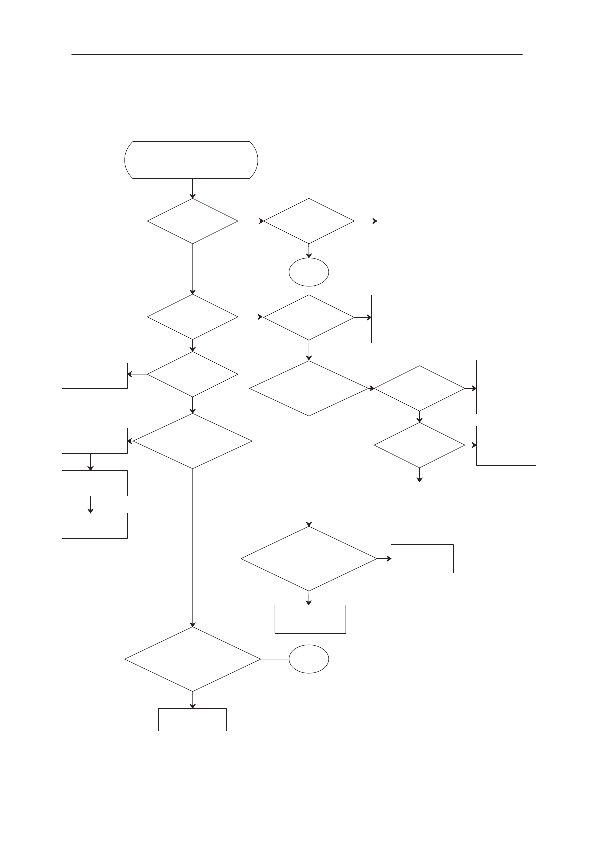
The purpose is to define fault block of the module and then find out the
broken component. The trouble shooting diagram has been planned so
that the fault, whatever it is, can be found by as simple measurements as
possible.
Required servicing equipment:
– PC for PCLocals
– Power supply (12 V 5 A)
– Digital multimeter
– Oscilloscope with 10:1 probes
– Spectrum analyzer (capable of 10 W input e.g. external attenuator)
– Signal generator
– Test SIM
Troubleshooting Instructions
– RF cables with BNC or N in the other end
– Modular cable
– RS232/M2BUS adapter DAU–2
– HP8922H
BB Troubleshooting Flow Diagrams
The baseband flow diagrams give you the overview of the blocks. The
purpose is that you proceed through the flow diagram so that, if your
answer is YES for the asked question, go straight to the next level, but if
your answer is NO, you have to go the sub–branch.
Original 08/97
Page 5
Page 6
NME–2A
Troubleshooting Instructions
Flash Programming OK; part 1
FLASH programming OK
P.A.M.S.
Technical Documentation
Check X102
C114 OK?
YES
R106 OK?
YES
Change N100
MBUS
registration
OK?
Power
stays on?
NO
NO
NO
VBATT
pins 4, 16 ?
YES
N100/pin 8/XRESET
+5 V after pwr on?
YES
YES
Display:
selftest failed
YES
3
Display:
selftest failed
YES
MBUS line X100/5
+5 V after pwr on?
YES
NO
NO
D250/MCU/pin 3
D300/ASIC/pin 97
rstrobe
Short circuits in data
data lines. data line
disconnected, VREF
unconnected
NO
R263
+ 5 V?
YES
V250 base
∼1 V
YES
Check R257
R260, R258,
V250, R268,
R270
If D250 at
NO
pin 66/TXD
doesn’t apply
+5 V change
NO
R262, R263
V250, V251
D250
Check
Page 6
Power supp. to the logic
circuits +5 V after pwr on?
NO
Change N100
MCU/D250/PIN67/RDX
+5 V after pwr on ?
NO
If R259 is OK
change D250
YES
2
YES
Change first
D250
Original 08/97
Page 7

P.A.M.S.
NME–2A
Technical Documentation
Flash Programming OK; part 2
Change D300
YES
NO
26 MHz clock
D300/pin 119?
NO
MCU/D250/pin 10
RESETX +5 V after
2
power on?
Troubleshooting Instructions
YES
26 MHz at MCU
/D250 pin 69
/MCUCLK?
YES
NO
Change D300
Check components
D301, D302, C306
R913, G902, C918
MCU/D250
/pin 8/MD2,
/pin 9/STNDBY?
YES
MCU/D250/pin 43
/XPWROFF pulses up to
+5 V after pwr on?
YES
MCU/D250/pin 77
/IRQ0 +5 V after
power on?
YES
MCU/D250/pin 4
/WSTROBEX +5 V
after pwr on?
NO
Check joints
NO
Change D250
NO
Change D300
NO
Check D300
and foils
Original 08/97
YES
Check all soldered joints
The data and address signals must
a clear difference between low (0 V)
and high (+5 V)
Page 7
Page 8

NME–2A
Troubleshooting Instructions
Flash Programming OK; part 3
MBUS registration OK?
Display: selftest failed?
P.A.M.S.
Technical Documentation
3
YES
YES
Check D300
Check D250
(D300)
Check D250
(D300)
EEPROM
initialization OK?
(FLASH8N.MES)
NO
NO
NO
NO
D253/EEPROM
/pin 27/EROMSELX pulses
+5 to 0 V during r/w
action?
YES
D253/EEPROM
/pin 1/RSTROBEX pulses
+5 to 0 V during r/w
action?
YES
D253/EEPROM
/pin 1/WSTROBEX pulses
+5 to 0 V during r/w
action?
YES
4
Page 8
YES
Change D253
Original 08/97
Page 9

P.A.M.S.
NME–2A
Technical Documentation
Flash Programming OK; part 4
/pin 64/RXD2 pulses
during programming?
4
D251/FLASH
/pin 11 +12 V during
programming?
YES
D250/MCU
YES
Troubleshooting Instructions
NO
NO
Check X100/pin 14
R271, L250, R264
R265, C264
Check X100/pin 6
R252, R253, R255
C254
X100/pin 7
/TXD2 pulses during
programming?
YES
D251/FLASH
/pin 12/PWD +5 V
after power on?
YES
D251/FLASH
/pin 9/ROMSELX pulses
from +5 to 0 V after
power on?
YES
D251/FLASH
/pin 37/RSTROBEX pulses
from +5 to 0 V after
power on?
NO
NO
NO
NO
Check D250/pin 63
R250, R251, C250
Check D300
Check D250 (D300)
Check D250 (D300)
Check D251/FLASH
ADDRESS/DATA LINES
/no shortcircuits or
unconnected pins allowed
OK
Change D251
Original 08/97
YES
/pin 38/WSTROBEX pulses
D251/FLASH
from +5 to 0 V after
power on?
NO
Check D250 (D300)
Page 9
Page 10

NME–2A
Troubleshooting Instructions
PWR Button Fault
Nothing happends
when PWR button
is pressed
P.A.M.S.
Technical Documentation
Check N101 pin 2
+6.2 V if not OK
change N101
NO
Check V106, L100
Change N100
NO
D250/pin 5,42 VL1
+5 V When XPWRON
is push high
YES
Check D250,
D300
N100/PSL pins
5,20 +6.2 V When either
XPWRON is low or
IGNS is high
YES
NO
pin 9/XPWROFF pulses
Check VL1, VL2, VA2, VREF
if OK then change N100
N100/PSL
from 0 to +5 V after
power on
YES
NO
VBATT voltage
YES
YES
Check V101
if OK change V110
N101/pin 4
V110 gate
is 0V
NO
Check
V102, V103,
V104, R109,
R110, R111,
R113, R133,
R134, C100
C112, C124
R143, V107
R100, R124
Page 10
Original 08/97
Page 11

P.A.M.S.
NME–2A
Technical Documentation
Display Selftest Failed
Display selftest failed or
phone doesn’t registrate to
the system (tester)
Use PCLocals to
find out a reason
MCU internal test
MCU RAM bus test
MCU ROM bus test
MCU IMEI test
NO
Troubleshooting Instructions
YES
Unprogrammed FLASH
Unconnected pins in MCU
address or data lines
MCU DSP code
download: failed,
DSP tests: no responce
RFI bus fault
NO
MCU audio codec
test: failed
YES
Codec N150/pin 12: PCMDO
Codec N150/pin 13: PCMDI
Codec N150/pin 19: PCMCLK
Codec N150/pin 20: XSELPCMC
YES
DSP clock oscillator
DSP pin 45/INT1
DSP pin 10/ERAMHI
DSP pin 9/IOX
DSP pin 12/EROM
DSP pin 14/RWN
DSP pin 15/EXM
DSP pin 39/RSTB
RFI/RFIAD 3:0
RFI/RFIDA 11:0
RFI pin 49/RDX
RFI pin 50/WRX
RFI pin 53/RFICLK
RFI pin 59/RFI2CLK
DSP RAM D201, D202
DSP/DSPDA
DSP/DSPAD
Original 08/97
Page 11
Page 12

NME–2A
Troubleshooting Instructions
No Registration to the System (no serv)
No registration to the
system (no svc)
no call
Selftest OK
YES
DSP pin 43, 45 INT0, 1 (from ASIC)
RFI pins 1,63/RXI, RXQ
RFI pin 3/EXTBG (4.096 V)
RFI pin 4/VCM (2.35 V)
RFI pin 6/TXC (to RF)
RFI pins 8,9/TXQ+, TXQ– (to RF)
RFI pins 11,12/TXI+, TXI– (to RF)
RFI pin 14/AFC (to RF)
RFI pins 20...23,28,29/PDA TA 5:0
RFI pin 51/DAX (to ASIC)
ASIC/D300/pin 105/SYNTHPWR (to RF)
ASIC/D300/pin 104/TXP (to RF)
ASIC/D300/pin 106/TXPPWR (to RF)
ASIC/D300/pin 111/SENAT (to RF)
ASIC/D300/pin 112/SENAR (to RF)
ASIC/D300/pin 113/SDAT (to RF)
ASIC/D300/pin 114/SCLK (to RF)
P.A.M.S.
Technical Documentation
Page 12
Original 08/97
Page 13

P.A.M.S.
NME–2A
Technical Documentation
Audio Fault
Audio fault
Microphone or earphone
signal missing
Microphone and
earphone signal
missing?
NO
Microphone signal
missing?
YES
YES
Troubleshooting Instructions
CODEC pin 15/SYNC (from ASIC)
CODEC pin 16/CODEC_CLK (from ASIC)
DSP pins 79, 82/PCMCOSYCLKX (from ASIC)
DSP pins 60, 81/PCMDATRCLKX (from ASIC)
DSP pin 80/CODEC_CLK
CODEC pin 21/HF_MIC
CODEC pin 22/MIC
CODEC pin 10/PCMOUT
NO
Earphone signal
missing?
YES
CODEC pins 6, 7/LSP
CODEC pins 3, 4/EAR
CODEC pin 14/PCMIN
DSP D200/pin 78
Original 08/97
Page 13
Page 14

NME–2A
Troubleshooting Instructions
RF Troubleshooting Instructions
The RF part consist of RX, TX and synthesizers as main blocks.
Interface to the rest of the radio is mainly through RFI.
In normal use, in the network, it is not possible to localize a malfunction to
any of these parts alone, because all of them may be needed to operate
the radio.
With a GSM tester like HP8922G/H it is possible to operate the radio in a
simple network like manner, and in that way localize some faults,
especially when you monitor the radio with PCLocals at the same time.
If the fault means, that the radio does not work with HP8922G/H then it is
possible via PCLocals in local mode, to operate the parts individually, and
in that way see if the parts can do what they are supposed to. It is also
possible to operate the parts dynamic, to check the switching between the
different modes, and that is more or less sufficient to tell if the RF is OK or
not.
P.A.M.S.
Technical Documentation
The following descriptions all starts with a simple and top level check. If
that fails or if the radio still has a malfunction, then the checks goes
deeper and deeper into the circuits to help finding the circuit that is
responsible for the malfunction.
RX Part
1. RSSI calibration (Input –57 dBm, channel 60, 947.06771MHz):
Checks the signal path from antenna to RFI and the AGC. The RFI
operates only as level detector in this mode. The offset value is a measure
of the total gain in the RX.
– –37 < Offset < 49 dB
– Calibration values between ±2 dB
– If it is OK, go to 2.
– If it fails then select via PCLocals RF control, Active unit RX, Operation
mode continuous, Continuous mode channel 60, AGC 93. Input –57
dBm 947.06771 MHz.
Measure with probe and oscilloscope or with the probe and spectrum
analyzer.
Page 14
Note: When measuring levels with an oscilloscope probe to the
spectrum analyzer, some calibration is needed!
Original 08/97
Page 15

P.A.M.S.
NME–2A
Technical Documentation
1.1. Check 13 MHz signal:
– RXI and RXQ > 0.3 VPP at 12.93 MHz.
– J702 input to 13 MHz filter > 0.5 V
– Check RXPWR J705 = 5 ±0.1 V
– Check 8.5 RX TX SW J703 = 7.7 ±0.1 V
1.2. Check 71/13 MHz mixer:
– N701, 71/13 MHz mixer: pin 15 4.8 ±0.2 V
– Enable: pin 21 > 4 V
– AGC5: <0.5 V (<2.5 V in burst)
– Output: J702 2.75 ±0.1 V
– LO: pin 6 >–10 dBm, 232 MHz
1.3. Check 71 MHz signal:
– AGC1 to AGC4 low (AGC4<2.5 V in burst)
Troubleshooting Instructions
PP
– N702: pin1 and pin14 4.8 V ±0.2 V
– Enable: pin 6 >4 V
– Input: pin12, 13 –50 dBm, 71 MHz
– Output: pin 4, 5 –10 dBm, 71 MHz
1.4. Check UHF mixer:
– LO C934: +9 dBm ±3 dB, 1014 MHz
– Signal in C722: –50 dBm, 947.07 MHz (–57 dBm input)
– Signal in C722: –30 dBm, 947.07 MHz (–37 dBm input)
– Signal out C726: –57 dBm, 70.93 MHz
1.5. Check 71 MHz amp:
– Output to filter: –35 dBm, 70.93 MHz
2. AFC (Input –57 dBm, channel 60, 947.06771MHz):
Checks the signal path, the VCXO and some parts of the demodulator.
The VCXO is tuned high, mid and low while the frequency deviation is
measured.
– 10 kHz < High < 20 kHz
– –5 kHz < Mid < 5 kHz
– –20 kHz < Low < –10 kHz
Original 08/97
Page 15
Page 16

NME–2A
Troubleshooting Instructions
2.1. Check the VCXO:
After AFC is done, the tuning voltage will stay high.
In other modes the tuning voltage will be in mid.
– Measure at J902: > 3 V
– High tuning: freq = 26 MHz +400 Hz ±100 Hz
– Low tuning: freq = 26 MHz –400 Hz ±100 Hz
– Mid tuning: freq = 26 MHz ±50 Hz
2.2. Check burst mode:
Select via PCLocals RF control, Active unit RX, Operation mode burst,
Continuous mode channel 60, AGC 93. Input –57 dBm 947.06771 MHz.
AGC is in that mode internally controlled.
P.A.M.S.
Technical Documentation
PP
Measure with scope ac coupled on RXI and RXQ, the output to RFI. Trig
the scope on RXPWR or 8.5RX TX SW or AGC0.
– Signal should be about 30 mV
– If not check the signal path and the LO signals as above.
3. Noise and sensitivity:
Checks the overall RX performance, except real demodulation.
Use F2 to measure clipping level and difference between I–Q.
Disconnect or switch off the RF signal from the generator.
Use F3 to measure SNR and Sensitivity.
– Clipping + SNR >50
– SNR > 20
– Sensitivity < –103 dBm
– I–Q < 1 dB
– If not repeat from 1 again.
4. Check camp on to HP8922G/H:
, and vary as the AGC operates.
PP
Page 16
Set HP8922G/H up with neighbors for its own BCCH and some empty and
some used channels. In cph use 3, 5, 20 (=own BCCH), 59 and 90.
Use PCLocals F8 to monitor the radio.
– RXlevel within ±2 dB from the BCCH level.
– RXlevel for empty neighbors less than 3.
– Decoding of the information in the used neighbors
– If not OK, the malfunction may be in the RFI and the circuits that con-
trol the RFI.
Original 08/97
Page 17

P.A.M.S.
NME–2A
Technical Documentation
TX Part
1. Check burst output:
Via PCLocals select local mode, RF control, TX mode, Power level 10
(23 dBm), Operation mode burst, Data type random, Continuous mode
channel 60, Channel 60, Monitoring channel 1.
Measure with spectrum analyzer on the antenna connector (40 dBm max
signal needs an external attenuator), and with scope on the power amps
control input pin 2.
– The output burst should have peak amplitude at 23 dBm ±3 dB, and
center at 902 MHz.
– If it is OK, check at higher and lower levels, up to level 2 (39 dBm) and
down to level 15 (13 dBm).
1.1. Check power tuning:
Troubleshooting Instructions
Via PCLocals select local mode, Power tuning.
– Coefficients from 0.8 at level 2 to about 0.1 at level 15.
– Tolerance of ±0.1 at level 2 to ±0.050 at level 15.
– The control signal should follow the RF amplitude with a maximum of 4
to 6 V at level 2 and 2 to 2.5 V at level 15.
1.2. TX buffer and level regulator:
Via PCLocals select local mode, RF control, TX mode, Power level 10
(23 dBm), Operation mode burst, Data type random, Continuous mode
channel 60, Channel 60, Monitoring channel 1.
Measure with spectrum analyzer on the antenna connector (40dBm max
signal needs an external attenuator), and with scope on the power amps
control input pin 2.
– If control signal goes up and RF does not follow, check with a probe
the RF input to the power amp at pin 1. It should be at 3 to 5 dBm.
– Follow the RF signal back to see if it is at the output of the balun T802.
– When measuring before the power amplifier continuous mode is pos-
sible.
Original 08/97
Page 17
Page 18

NME–2A
Troubleshooting Instructions
1.3. Modulator and LO signal generation:
Via PCLocals select local mode, RF control, TX mode, Power level 10
(23 dBm), Operation mode continuous or burst, Data type random,
Continuous mode channel 60, Channel 60, Monitoring channel 1.
Measure with oscilloscope probe and spectrum analyzer.
– Output of modulator on T802: –10 dBm ±5 dB.
– Input to the modulator consist of three discrete frequencies, where the
wanted is the lowest frequency, and at a level about 15 dB higher than
the other two. Absolute level about –10 dBm for the wanted signal.
– Check the LO generating mixer (UHF TX and VHF RX PLL), the ampli-
fier and the filter.
– UHF LO: 5 dBm ±5 dB, 1014 MHz
– VHF RX PLL: –5 dBm ±5 dB, 116 MHz
P.A.M.S.
Technical Documentation
– Check the modulating input, balanced pairwise for I and Q, about 1
Vpp for every signal, d.c. at 2.4 V.
– Check the power and enable to the modulator.
– Check the UHF and VHF synthesizers.
2. Modulation spectrum:
Select I and Q TUNING in PCLocals. Measure with spectrum analyzer on
the antenna connector (up to 40 dBm output!). Span 0.2 MHz, resolution
BW 10 kHz, video 10 kHz, sweep time 0.5 sec.
– Relative to the mainslope the signal at +67 kHz should be more than
30 dB down, and the signal at +135 kHz should be more than 50 dB
down.
– If not tune the offset values, I and Q d.c. offset to change the signal at
+67 kHz, phase and amplitude offset to change the signal at
+135 kHz.
Page 18
Original 08/97
Page 19

P.A.M.S.
NME–2A
Technical Documentation
UHF Synthesizer
Via PCLocals select local mode, RF control, TX mode, Power level 10
(23 dBm), Operation mode burst, Data type random, Continuous mode
channel 60, Channel 60, Monitoring channel 1. The synthesizer will switch
between channel 60 and channel 1.
– Freq. ch 1 = 1006.2 MHz, ch 124 = 1039.8 MHz.
– Measure with probe and scope on J904 to see the tuning voltage. It
should switch between 1 and 2 volt. Select channel 124 and it should
switch between 1 and 4.5 volt.
– J902, 26MHz ref: 26 MHz, >2 V
– Measure at the collector of V904 (UHF TX) and of V906 (LO UHF) to
see that they alternately are on.
– With a probe connected to the spectrum analyzer, check the RF sig-
nals. The level when they are active should be about 6 dBm.
Troubleshooting Instructions
PP
VHF Synthesizer
Via PCLocals select local mode, RF control, TX mode, Power level 10
(23 dBm), Operation mode burst, Data type random, Continuous mode
channel 60, Channel 60, Monitoring channel 1.
– Freq. all channels = 232 MHz. The prescaler is placed in V701 and di-
vides the frequency with 2.
– Check the tuning voltage at J903, 3 ±1.5 V, and check that it moves
when a finger is placed at the oscillator.
– J902, 26 MHz ref: 26 MHz, >2 V
– Check the supply at V902 or C903, 5 V.
– Output level at C914/R911 should be –10 dBm.
PP
Original 08/97
Page 19
Page 20

NME–2A
Troubleshooting Instructions
P.A.M.S.
Technical Documentation
[This page intentionally left blank]
Page 20
Original 08/97
 Loading...