

Page 1

Nokia Customer Care
6(b) - RF Troubleshooting
Instructions
Issue 1 04/2005 COMPANY CONFIDENTIAL
Copyright © 2005 Nokia. All Rights Reserved.
Page 2

RM-94
Nokia Customer Care 6(b) - RF Troubleshooting Instructions
This page has been intentionally left blank.
2 COMPANY CONFIDENTIAL Issue 1 04/2005
Copyright © 2005 Nokia. All Rights Reserved.
Page 3

RM-94
6(b) - RF Troubleshooting Instructions Nokia Customer Care
Table of Contents
Page No
General Information on RF Troubleshooting ................................................... 5
Test environment............................................................................................... 5
Test conditions................................................................................................... 5
Receiver Verification and Troubleshooting...................................................... 7
General instructions for RX troubleshooting ...................................................... 7
Measuring RX I/Q signals using RSSI reading .................................................. 7
Measuring RX performance using SNR measurement .................................... 8
Measuring front-end power levels using spectrum analyzer ............................ 9
Measuring analogue RX I/Q signals using oscilloscope ................................10
Fault finding chart of the receiver..................................................................... 11
Transmitter ........................................................................................................ 18
General instructions for TX troubleshooting..................................................... 18
GSM900 transmitter......................................................................................... 18
General instructions for GSM900 TX troubleshooting ................................... 18
Fault finding chart for GSM900 transmitter ....................................................20
GSM1800 transmitter....................................................................................... 22
General instructions for GSM1800 TX troubleshooting ................................. 22
Fault finding chart for GSM1800 transmitter .................................................. 24
GSM1900 transmitter....................................................................................... 26
General instructions for GSM1900 TX troubleshooting ................................. 26
Fault finding chart for GSM1900 transmitter .................................................. 28
Synthesizer........................................................................................................31
General instructions for synthesizer troubleshooting....................................... 31
Checking synthesizer operation....................................................................... 31
Fault finding chart for PLL synthesizer............................................................. 34
Frequency tables ............................................................................................. 36
GSM900 (including EGSM900) ...................................................................... 36
GSM1800 .......................................................................................................37
GSM1900 .......................................................................................................38
DC Supply Voltage Check ................................................................................39
Receiver test points ......................................................................................... 42
Transmitter test points ..................................................................................... 44
Synthesizer test points..................................................................................... 47
Issue 1 04/2005 COMPANY CONFIDENTIAL 3
Copyright © 2005 Nokia. All Rights Reserved.
Page 4

RM-94
Nokia Customer Care 6(b) - RF Troubleshooting Instructions
This page has been intentionally left blank.
4 COMPANY CONFIDENTIAL Issue 1 04/2005
Copyright © 2005 Nokia. All Rights Reserved.
Page 5

RM-94
6(b) - RF Troubleshooting Nokia Customer Care
General Information on RF Troubleshooting
Notes:
Several bills of material (BOM): There are two different kinds of VCOs, VCTXOs, RF-PAs, SAW-
filters and Antenna Switches (ASM) assembled. They may only be rep laced with the same type
as the original component (from the same manufacturer).
Phoenix version: In this document there are example measurements being depicted with pictures of AMS-Phoenix, version A 2004.06.1.69. In later versions pictures of menus and windows
may look differently.
Layout version: The drawings of test points and component placement in this version of the do cument are taken from build B4.0 layout (1gqa_41a). If you use the document for newer layout
versions, make sure to use the corresponding assembly and test point drawings.
■ Test environment
It is assumed, that the phones are disassembled and tested with a repair jig MJ-22R.
The following measurements have to be done for repairing the phone boards:
• RF measurements shall be done using a spectrum analyzer together with a highfrequency probe. Note that the signal will be significantly attenuated. Correct attenuation can be checked using a “good” phone board for example.
• LF (low frequency) and DC measurements shall be carried out with an oscillo-
scope together with a 10:1 probe.
• For receiver measurements, a signal generator specified for frequencies up to
2000 MHz is required. The signal generator is connected to the antenna port of the
repair jig.
Most of the radio communication testers, like CMU200, can be used as a signal generator, but make sure to have a continuous (CW) signal without modulation for alignment purposes.
• Transmitter output level measurements shall be done with a power meter
which is connected to the antenna port of the repair jig.
Always make sure that the measurement set-up is calibrated when measuring RF parameters
at the antenna port. Remember to put the correct losses of the module repair jig and the connecting cable in Phoenix or in the set-up programs of the RF generators when realigning the
phone.
Apart from key-components described in this document, there are a lot of discrete compone nts
(resistors, inductors and capacitors) for which troubleshooting has to be done by checking its
proper soldering and complete assembly on the PWB. Capacitors and resistors can be
checked by means of an ohm-meter , but be aware in -circuit measurement s should be evaluated carefully.
■ Test conditions
Rx tuning of the 26 MHz reference oscillator (VCTCXO) is temperature sensitive because
of the estimations of <AFC_value> and <AFC_slope>. According to the Production Test Specification DCS02294-EN-0.5, the ambient temperature has to be within a temperature range of
22°C to 28°C.
Issue 1 04/2005 COMPANY CONFIDENTIAL 5
Copyright © 2005 Nokia. All Rights Reserved.
Page 6

RM-94
Nokia Customer Care 6(b) - RF Troubleshooting
Most RF semiconductors are static discharge sensitive. ESD prote ction must be taken into
account during repair (ground straps and ESD soldering irons).
The RF ASIC Helgo is moisture sensitive. Therefore, the ASIC must be pre-baked prior to
soldering.
6 COMPANY CONFIDENTIAL Issue 1 04/2005
Copyright © 2005 Nokia. All Rights Reserved.
Page 7

RM-94
6(b) - RF Troubleshooting Nokia Customer Care
Receiver Verification and Troubleshooting
■ General instructions for RX troubleshooting
Connect the phone to a PC, which has Phoenix Service Software an d a dongle installed, using
either
• repair jig and DAU-9S (RS232) cable or
• repair jig and XCS-4 cable via FPS-8 Flash Box or
• DAU-9T cable (RS232).
Connect the phone to a power supply (DC voltage: 3.6V, max. current: 3A) and an RF signal
generator. Switch the phone on.
Start Phoenix Service Software and open FBUS connection.
Select Scan Product Ctrl-R
and wait until the phone information (RM-94) is shown in the lower right corner of the screen.
Follow the instructions below.
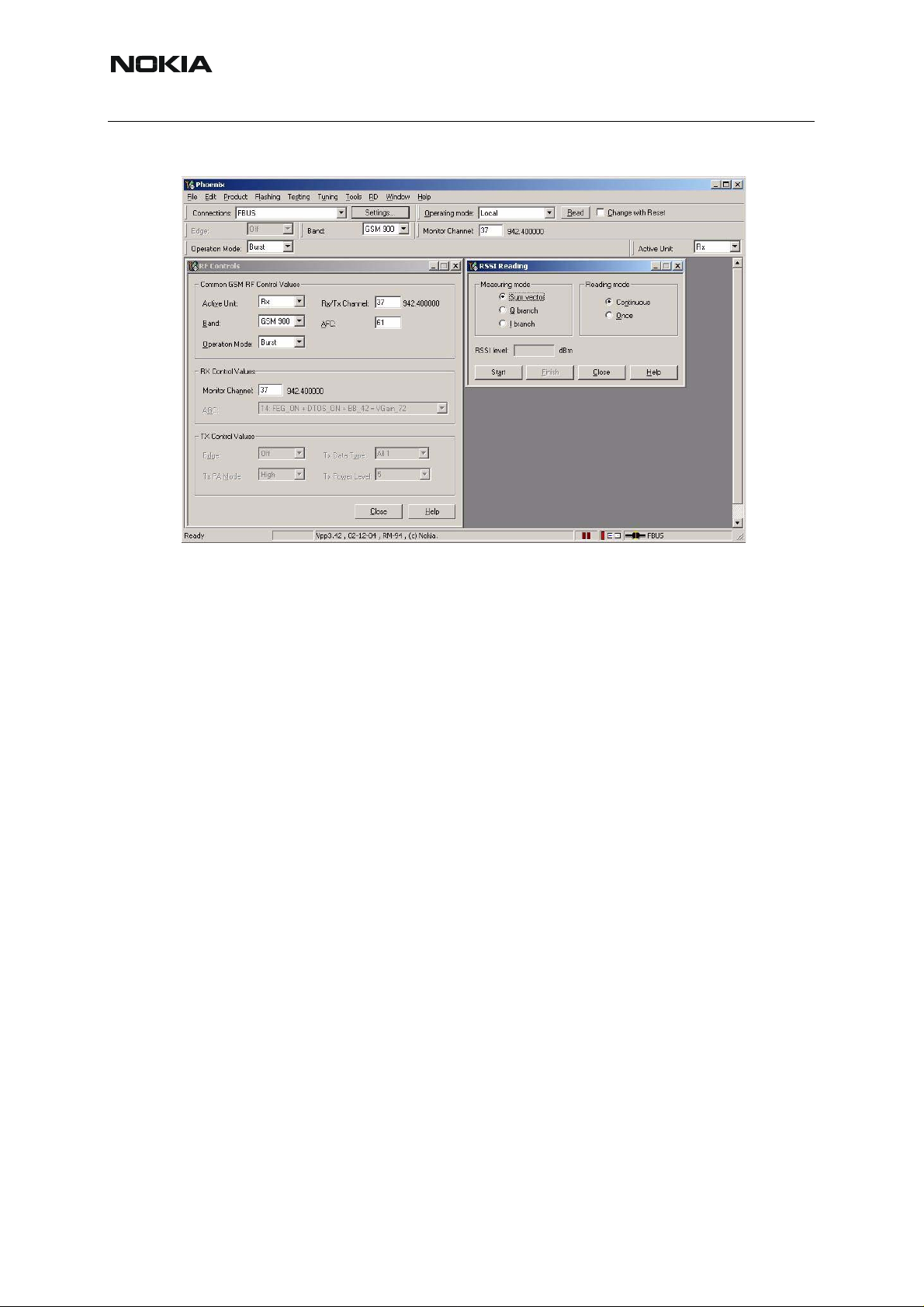
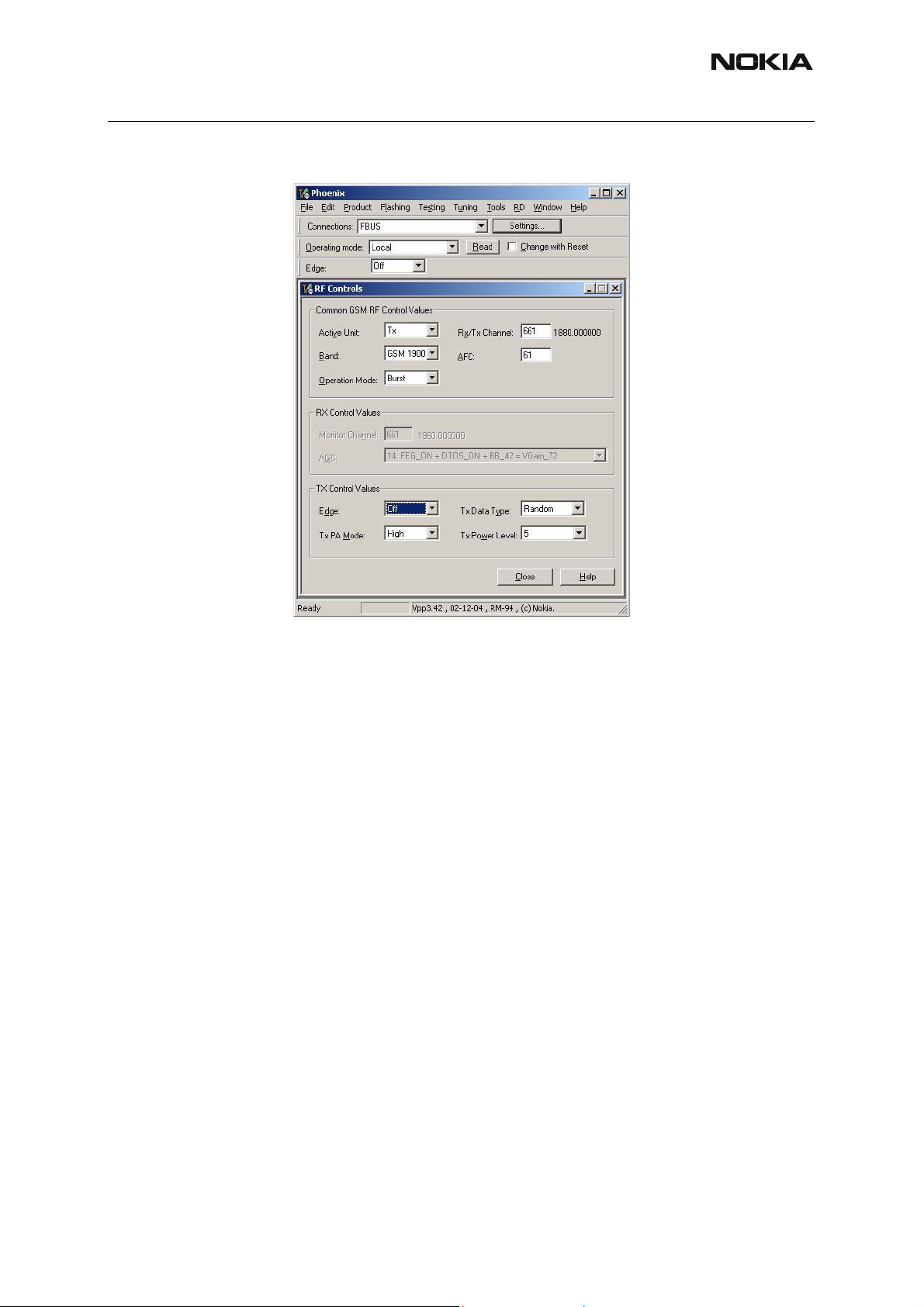
■ Measuring RX I/Q signals using RSSI reading
Start Phoenix Service Software and open FBUS connection.
Select Scan Product Ctrl-R
Wait until the phone information is shown in the lower right corner of the screen.
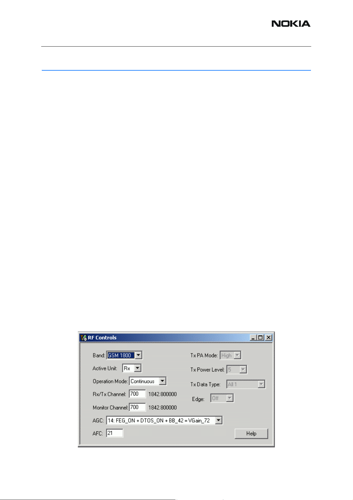
Set the operating mode to local mode
Select Testing T
RF Controls F
Select Band GSM 900 or GSM1800 or GSM1900
Active unit RX
Operation mode Burst
RX/TX Channel 37 or 700 or 661
Select Testing T
RSSI reading
In the RSSI Reading window, the <measuring mode> shall be set on Sum vector and the
<reading mode> on Continuous.
The set up should now look like this:
Issue 1 04/2005 COMPANY CONFIDENTIAL 7
Copyright © 2005 Nokia. All Rights Reserved.
R
Page 8
RM-94
Nokia Customer Care 6(b) - RF Troubleshooting
(The example below shows a screen shot in GSM900!)
Make the following settings on your signal generator:
Frequencies:
• GSM 900: 942.46771 MHz (channel 37+ 67.710 kHz offset)
• GSM 1800: 842.86771 MHz (channel 700 + 67.710 kHz offset)
• GSM 1900: 1960.06771 MHz (channel 661+ 67.710 kHz offset)
RF power level:
• – 80 dBm @ the antenna connector of the phone/ test jig
(remembering to compensate for the cable and jig attenuation).
Click on <Read now> in RSSI reading.
The resulting RSSI level shall be – 80 dBm +/– 0.5 dB in each band.
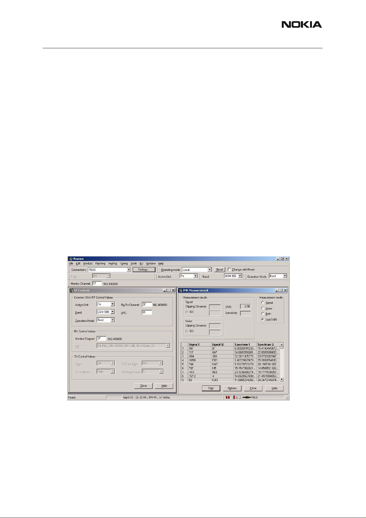
Measuring RX performance using SNR measurement
Start Phoenix Service Software and open FBUS connection.
Select Scan Product Ctrl-R
Wait until the phone information is shown in the lower right corner of the screen.
Set operating mode to <local mode>.
Select Testing T
RF Controls F
Select Band GSM 900 or GSM1800 or GSM1900
Active unit RX
8 COMPANY CONFIDENTIAL Issue 1 04/2005
Copyright © 2005 Nokia. All Rights Reserved.
Page 9
RM-94
6(b) - RF Troubleshooting Nokia Customer Care
Operation mode Burst
RX/TX Channel 37 or 700 or 661
Select Testing T
SNR Measurement M
Select Measuring mode Fast SNR (Radio Button)
Press Start
The window <Signal Measurement> pops up informing on frequency and power level of the
signal generator to be set. Follow the command <Turn ON the RF generator>.
Press <ok> and the window will close.
Read the SNR result from the window SNR Measurement. The value shall exceed:
• GSM 900: > 20 dB
• GSM 1800: > 18 dB
• GSM 1900: > 18 dB
The set up should now look like this:
(The example below shows a screen shot in GSM900!)
Choose the remaining GSM bands and measure accordingly the procedure described above.
Measuring front-end power levels using spectrum analyzer
Spectrum analyzer (SA) level values depend on the probe type and shall be verified by a properly working phone sample. The levels that are given in this document are measured with a resistive probe (50 Ohm semi-rigid cable).
Start Phoenix Service Software and open FBUS connection.
Issue 1 04/2005 COMPANY CONFIDENTIAL 9
Copyright © 2005 Nokia. All Rights Reserved.
Page 10

RM-94
Nokia Customer Care 6(b) - RF Troubleshooting
Select Scan Product Ctrl-R
Wait until the phone information is shown in the lower right corner of the screen.
Set <operating mode> to <local mode>.
Select Testing T
RF Controls F
Select Band GSM 900 or GSM1800 or GSM1900
Active unit RX
Operation mode Continuous
RX/TX Channel 37 or 700 or 661
Please refer to the fault finding chart and Appendix for proper levels at different test points.
Measuring analogue RX I/Q signals using oscilloscope
Measuring with an oscilloscope RX I and RX Q signals on the test points <RXI> respectively
<RXQ> is recommended only if the RSSI reading does not provide enough information. Input
level = -60dBm.
Start Phoenix Service Software and open FBUS connection.
Select Scan Product Ctrl-R
Wait until phone information is shown in the lower right corner of the screen.
Set operating mode to <local mode>.
Select Testing T
RF Controls F
Wait until the RF Controls
Select Band GSM 900 or GSM1800 or GSM1900
window pops up.
Active unit RX
Operation mode Continuous
RX/TX Channel 37 or 700 or 661
AGC 10
The following picture should be displayed on an oscilloscope's screen if the receiver is working
properly:
10 COMPANY CONFIDENTIAL Issue 1 04/2005
Copyright © 2005 Nokia. All Rights Reserved.
Page 11

RM-94
6(b) - RF Troubleshooting Nokia Customer Care
Signal amplitude 1.40Vpp
DC offset ª 1.28V as the offset is floating, switch to the operating mode
<Burst> in Phoenix and read the DC offset
Frequency 67kHz
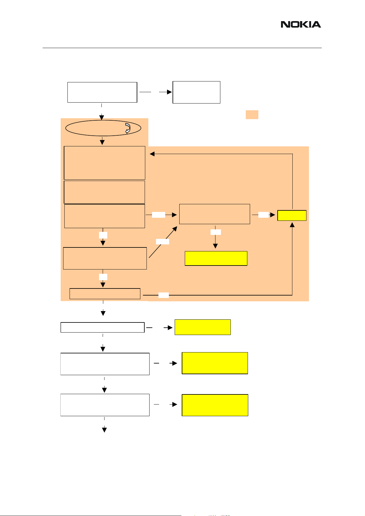
■ Fault finding chart of the receiver
During fault finding, the calibration procedure is used to find out, whether all bands are affected
(error in common part of the Rx chain) or only one band (error in a Rx part of the failed band).
Take care not to save calibration values to the phone memory, which are out of limits.
Find the error first and repair it.
When a defective phone has been calibrated, a possible error in RX front-end might be
masked. In that case, one can get a reasonable RSSI reading, although the front-end shows
excessive losses. If it is not sure that incorrect re-calibration has been made, following steps
shall be carried out:
• Check if AGC calibration is within limits.
• Check if SNR reading is o.k.
Use an oscilloscope to check levels of “RXI” and “RXQ”.
The RF ASIC generates only single ended I and Q signals (RXI, RXQ). As the A/D converter
in UEM requires two differential signals, an artificial mid voltage is generated from VrefRF02.
The phone layout has dedicated test points for the analogue RX I and Q signals (J512, J513).
The BB part is used to measure those signals by means of RSSI reading. This works only if
correct calibration has been carried out in production.
Issue 1 04/2005 COMPANY CONFIDENTIAL 11
Copyright © 2005 Nokia. All Rights Reserved.
Page 12
RM-94
Nokia Customer Care 6(b) - RF Troubleshooting
RSSIreading [dBm] = 20log(UBB/U
LSB
) - AGC
calibrated
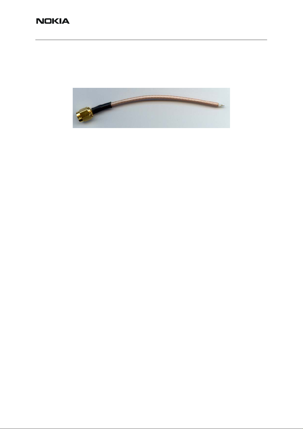
In order to check the levels and frequencies of RF signals, the following probe can be used
(note that only the core lead contacts the test point, the shield ing of the coaxial cable does not
contact GND during the measurement):
Connect this probe via a coaxial cable and a DC block to a spectrum analyzer. The DC block
is important to protect the spectrum analyzer from DC levels, which superpose the RF signal
at several test points.
If both RX and TX path seem to be faulty, it has to be checked if the synthesizer is working.
12 COMPANY CONFIDENTIAL Issue 1 04/2005
Copyright © 2005 Nokia. All Rights Reserved.
Page 13
RM-94
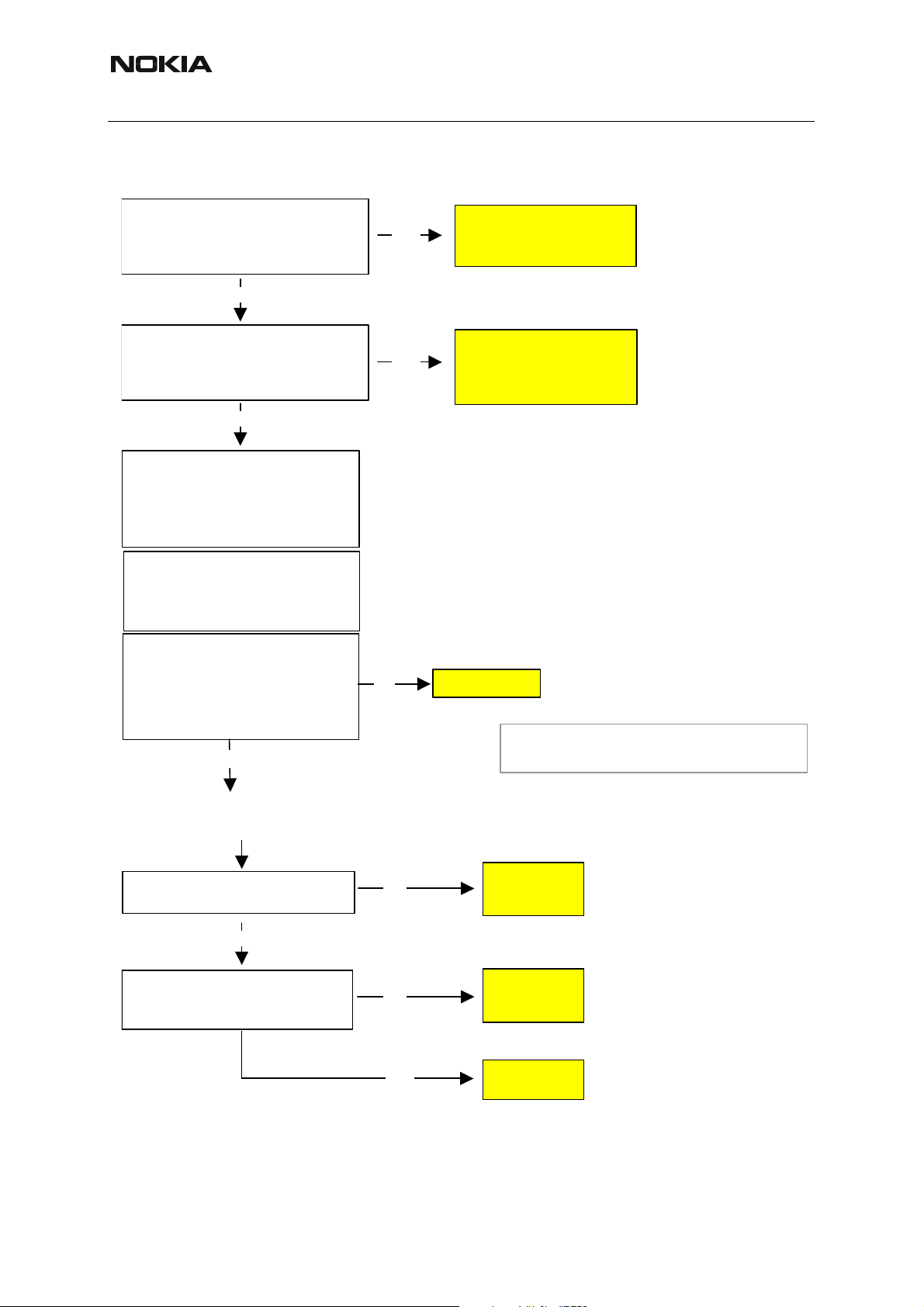
A
A
A
6(b) - RF Troubleshooting Nokia Customer Care
Phoenix:
Phone: local mode
Open
Signal Generator:
Phoenix:
Open
Check RSSI Level = -80dBm
Execute Rx Calibration in selected
band, refer to chapter 9.2.1
re calibration results within limits?
Make sure that
Synthesizer is working
Yes
All 3 bands
RF Controls
Active Unit: Rx
Op. Mode: Burst
Rx/Tx channel: default (mid)
Level: –80dBm
Frequency: calculated from
Phoenix + 67.71kHz
RSSI reading
No
:
see
No
Yes next bandNo
Synthesizer Fault
Finding Tree
Yes
Selected band is working and
calibrated.
re all 3 bands measured?
Yes
Rx chain is functional
and calibrated
Receiver
Fault Finding Tree
part 1
= To be done in all
three bands.
No
re all 3 bands measured?
Yes
Are all 3 bands defective?
Yes
Oscilloscope:
Check supply voltages of RF ASIC:
VR4 = 2.8V ? (TP: VR4)
Yes
Oscilloscope:
Check supply voltages of RF ASIC:
VR6 = 2.8V ? (TP:VR6)
Yes
No
No
Continue with single
band fault finding.
No
No
Check supply filter
components (C2233,
C7519, C7520) and UEM
Check supply filter
components (C2231,
C7521) and UEM
Receiver
Fault Finding Tree
part 2
Receiver
Fault Finding Tree
part 3
Issue 1 04/2005 COMPANY CONFIDENTIAL 13
Copyright © 2005 Nokia. All Rights Reserved.
Page 14
RM-94
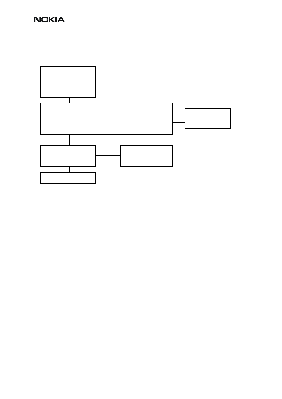
r
Nokia Customer Care 6(b) - RF Troubleshooting
Oscilloscope:
Check reference voltages of RF part:
VrefRF01 = 1.35V ?
(TP: VrefRF01*)
Yes
No
Check supply filter
components (R7511,
C7524) and UEM
Receiver
Fault Finding Tree
part 4
Oscilloscope:
Check reference voltages of RF part:
VrefRF02 = 1.35V ?
(TPs: VrefRF02* and VrefRF02**)
Yes
Phoenix:
Phone: local mode
RF Controls
Active Unit: Rx
Op. Mode:
Rx/Tx channel: default (mid)
AGC: 14
:
Continuous
Signal Generator:
To be tuned that input power at spectrum
analyzer: –60dBm
(power at probe:
Frequency: calculated from Phoenix
offset: 67.71kHz
= approx. -63 dBm)
Pref
Spectrum Analyzer: 1)
Check Rx/Tx Switch (Diplexer)
Depending on selected band, check level at TPs:
GSM900 output Rx1 Pref -1.5dB ?
GSM1800 output Rx2 Pref -2.0dB ?
GSM1900 output Rx3 Pref -2.5dB
Yes
Check supply filter
No
components (R2900,
R2901, C2900, C2901)
and UEM
Receive
Fault Finding Tree
part 5
No
?
Change Z7800
Note 1):
RF levels are dependent on RF probe and have to be validated
with a known good sample.
Oscilloscope:
RX IQ levels ok (TPs: RXI, RXQ) ?
Yes
Oscilloscope:
RF-BB serial interface ok?
(TPs: RFBusData, RFBusClk, RFBusEna1)
No
No
Yes
Change RF
ASIC (Helgo)
BB error:
Check UPP
Change RF
ASIC (Helgo)
Receiver
Fault Finding Tree
part 6
14 COMPANY CONFIDENTIAL Issue 1 04/2005
Copyright © 2005 Nokia. All Rights Reserved.
Page 15

RM-94
6(b) - RF Troubleshooting Nokia Customer Care
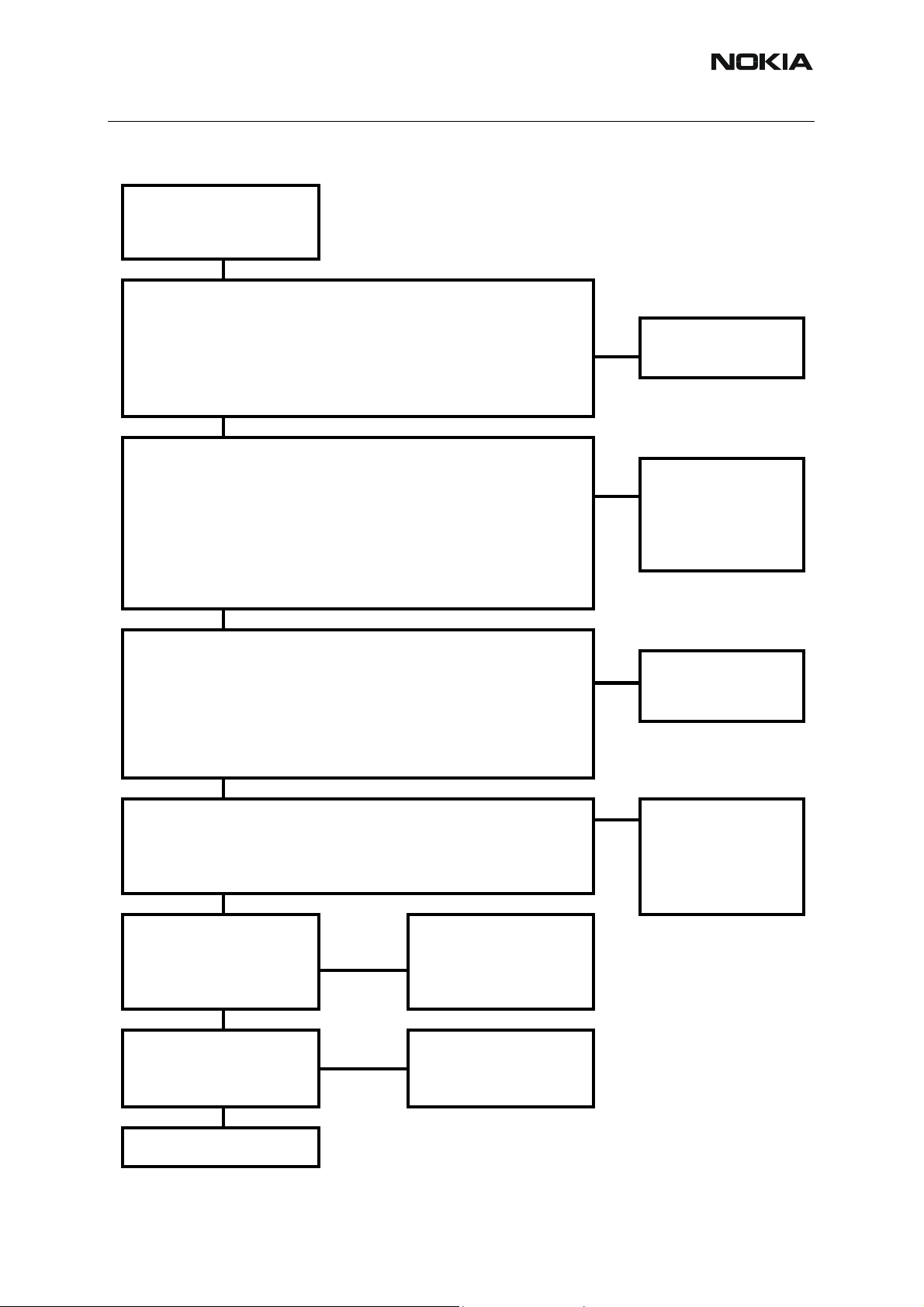
Select faulty band in Phoenix and continue measurements on dedicated Rx part.
Phoenix:
SNR Measurement
open
Meas. Mode: Fast SNR
Measure
Press
Signal Generator:
Level: –92dBm
Frequency: calculated from Phoenix
Phoenix:
SNR measurement ok?
(SNR > 18.37dB)?
Phoenix:
Phone: local mode
RF Controls
Active Unit: Rx
Op. Mode:
Rx/Tx channel: default (mid)
AGC: 14
.
No
:
Continuous
Single band fault finding
Receiver
Fault Finding Tree
part 7
Yes
Front end is ok.
Phoenix:
Phone: local mode
RF Controls
Active Unit: Rx
Op. Mode:
Rx/Tx channel: default (mid)
AGC: 10
:
Continuous
Signal Generator:
Level: –60dBm
Frequency: calculated from Phoenix
offset: 67.71kHz
Continue with Rx Fault Finding part 6.
Receiver
Fault Finding Tree
part 8
Signal Generator:
To be tuned that input power at spectrum
analyser: –60dBm
power at probe:
Frequency: calculated from Phoenix
offset: 67.71kHz
=approx. -63dBm)
Pref
Spectrum Analyzer: 1)
Center Freq: calculated from Phoenix
RBW 20kHz
Check Rx SAW filter and matching
network of selected band:
GSM900 TPs: INM_G_RX / INP_G_RX
both output levels > Pref -3.5dB ?
GSM1800 TPs: INM_D_RX / INP_D_RX
both output levels > Pref -6dB ?
Yes
No
Note 1):
RF levels are dependent on RF probe and have to be validated
with a known good sample.
Change Rx SAW filters (Z7802,
Z7803) or component(s) of
matching network depending on
selected band
Issue 1 04/2005 COMPANY CONFIDENTIAL 15
Copyright © 2005 Nokia. All Rights Reserved.
Page 16

RM-94
g
1)
Nokia Customer Care 6(b) - RF Troubleshooting
If selected band = GSM1900
Spectrum Analyzer:
Check SAW filter Z7801:
TP: OUT-Z7801
Output signal > Pref - 3.5dB
No
Spectrum Analyzer:
Check external LNA V7800:
TP: OUT-V7800
Output signal > Pref +14dB
Spectrum Analyzer:
Check balun T7800 and matching network:
TPs: INM_P_RX / INP_P_RX
Both output signals > Pref +12dB
RF ASIC N7500 seems to be
defective. Exchange N7500.
Yes
Yes
Yes
Yes
No
Yes
1)
No
1)
Oscilloscope:
Check voltages for V7800:
No
Voltage at C7802 = 2.5V ?
e at C7800 = 0V ?
Volta
Receiver
Fault Finding Tree
part 9
Change Z7801
Check supply
No
around V7800
filter components
and RF ASIC
Yes
No
Note 1):
RF levels are dependent on RF probe and have to be validated
with a known good sample.
Change T7800
16 COMPANY CONFIDENTIAL Issue 1 04/2005
Copyright © 2005 Nokia. All Rights Reserved.
Page 17

RM-94
6(b) - RF Troubleshooting Nokia Customer Care
Make sure that Synthesizer is
working and supply voltages of
RF ASIC are ok
Phoenix:
Phone: local mode
RF Controls
Active Unit: Rx
Op. Mode:
Rx/Tx channel: default (mid)
AGC: 14
:
Burst
Continue measurement only when channel select filter calibration failed
Channel select filter fault finding
Receiver
Fault Finding Tree
part 10
Signal Generator:
Level: –60dBm
Frequency: 942.4MHz
Offset: 67.71kHz
Oscilloscope:
RF-BB filter signals ok?
TPs: CM_F_Q & CM_F_I
CM_DTOS_Q & CM_DTOS_I
Yes
Repair finished
No
Re-solder capacitor array C7523
Re-calibrate
Channel Select Filter
Calibration ok ?
NoYes
Change RF
ASIC (Helgo)
Make following tunings/calibrations
Tx power l evel tuning
x
Tx IQ tuning
x
x Rx calibration
Rx Band Filter Response Calib.
x
Issue 1 04/2005 COMPANY CONFIDENTIAL 17
Copyright © 2005 Nokia. All Rights Reserved.
Page 18

RM-94
Nokia Customer Care 6(b) - RF Troubleshooting
Transmitter
■ General instructions for TX troubleshooting
Connect the phone to a PC, which has Phoenix Service Software an d a dongle installed, using
either
• repair jig and DAU-9S (RS232) cable or
• repair jig and XCS-4 cable via FPS-8 Flash Box or
• DAU-9T cable (RS232)
Connect the phone to a power supply (DC voltage of 3.6V) and switch the phone on. The value
of the DC voltage of 3.6V at the phone battery connector is crucial.
Connect an RF cable between the test jig and the measurement equipment (GSM test equip-
ment, power meter, spectrum analyzer, or similar).
Make use of an adequate attenuator at the input of your measurement equipment (10dB to
20dB are recommended for a spectrum analyzer or a power meter). Additionally, a DC block is
recommended. Assure not to overload or destroy the equipment.
It is strongly recommended to use TXP as external trigger for all TX tunings. External triggering
gives the following advantages:
• trigger for spectrum analyzer (gated sweep)
• trigger for oscilloscope
• trigger for power meter (avoid exchanging of attenuator and getting better accu-
racy in power measurements)
Start Phoenix Service Software and open FBUS connection:
Select Scan Product Ctrl-R
and wait until the phone information is shown in the lower right corner of the screen.
Follow the instructions in the chapters below.
■ GSM900 transmitter
General instructions for GSM900 TX troubleshooting
Start the preparations as described in chapter “General instructions for TX troubleshooting”.
GMSK
Set operating mode to local mode.
Select Testing RF Controls
Wait until the RF Controls window pops up
Select Band GSM 900
Active unit TX
18 COMPANY CONFIDENTIAL Issue 1 04/2005
Copyright © 2005 Nokia. All Rights Reserved.
Page 19

RM-94
6(b) - RF Troubleshooting Nokia Customer Care
Operation mode Burst
RX/TX Channel 37
TX Power Level 10
TX Data Type Random
Edge Off
The setup should now look like this:
Now the measurement equipment should detect the following output signal of the phone:
P
= +23dBm @ 897.4 MHz
out
If this is not the case, go to the GMSK fault finding chart for the GSM900 transmitter.
EDGE
Set operating mode to local mode.
Select Testing RF Controls
Wait until the RF Controls window pops up.
Select Band GSM 900
Active unit TX
Operation mode Burst
Issue 1 04/2005 COMPANY CONFIDENTIAL 19
Copyright © 2005 Nokia. All Rights Reserved.
Page 20

RM-94
Nokia Customer Care 6(b) - RF Troubleshooting
RX/TX Channel 37
TX Power Level 10
TX Data Type All1
Edge On
The setup should now look like this:
Now the measurement equipment should detect the following output signal of the phone:
P
= +24.5 dBm @ 897.4 MHz
out
If this is not the case, go to the EDGE fault finding chart for GSM900 transmitter.
Fault finding chart for GSM900 transmitter
In the following, it is assumed that the TXP signal is used as trigger signal. For that, a TXP test
point is provided.
20 COMPANY CONFIDENTIAL Issue 1 04/2005
Copyright © 2005 Nokia. All Rights Reserved.
Page 21

RM-94
6(b) - RF Troubleshooting Nokia Customer Care
GMSK
Use Phoenix to select
TX_Data Type: Random
TX Power Level: 10
Ch37
Ensure Vbatt=3.6 V
Yes
Oscilloscope
C7711
R7511
C7512
TXP testpoint
C7517
R7516
Yes
Oscilloscope
C7529
C7529
C7530
C7530
Yes
Oscilloscope
C7701
VC1
VC2
VC3
R7713
Yes
Spectrum analyzer No Check
Z7700 out, R7704 in RFin_850/
Compare with good
Yes Synthesizer
Mode
VREF01
VR2
TXP
VR5
VR3
TXIOUTP
Vdc = 1.35 Volt Check
Vdc = 2.78 Volt No Baseband
V = 1.8 Volt
Vdc = 2.78 Volt
Vdc = 2.78 Volt
V = 0 Volt
67kHz
No Check
Vac = 0.45 Vpp, Vdc =
1.2 V
TXIOUTN
67kHz
Baseband
Vac = 0.45 Vpp, Vdc =
1.2 V
TXQOUTP
67kHz
Vac = 0.45 Vpp, Vdc =
1.2 V
TXQOUTN
67kHz
Vac = 0.45 Vpp, Vdc =
1.2 V
VTXB_900
CONT1
CONT2
CONT3
VPCTRL_90
0
V = 2.78 Volt No Check:
V = 0 Volt Helgo Serial Interface
V = 0 Volt Helgo
V = 2.7 Volt
V = 1.17 Volt
P>= 2 dBm, 897.4MHz EGSM TX SAW Filter
900
Helgo
sample
Spectrum analyzer Check PA N7700
Z7800 TX1 (PA N7700
RFOut_850/900)
Power = +24.3 dBm,
No Check Power Loop
(TXC, Vpctrl900, DET)
897.4 MHz
Yes
Spectrum analyzer Check
RF@Test-Jig No
Pout
Antenna Switch (Z7800)
= +23 dBm, 897.4 MHz
Yes
GSM900 TX
OK
Issue 1 04/2005 COMPANY CONFIDENTIAL 21
Copyright © 2005 Nokia. All Rights Reserved.
Page 22
RM-94
Nokia Customer Care 6(b) - RF Troubleshooting
EDGE
Ensure that GMSK is ok.
Use Phoenix to select
TX_Data Type: All 1
EDGE: On
TX Power Level: 10
Ch37
Ensure Vbatt=3.6 V
Yes
Oscilloscope
C7702
C7711
VPCTRL_900
Yes
Spectrum analyzer Check PA N7700
RF@Test-Jig No Check Power Loop
Pout
= +24.5 dBm, 897.4MHz
Yes
GSM900 TX
OK
IREF01
Mode
R7713
(TXC,Rfin 900, DET)
V ~ 1.77 Volt Check
V = 1.8 Volt No Baseband
V= 2.7 V
■ GSM1800 transmitter
General instructions for GSM1800 TX troubleshooting
Start the preparations as described in chapter “General instructions for TX troubleshooting”.
GMSK
Set operating mode to local mode.
Select Testing RF Controls
Wait until the RF Controls window pops up
Select Band GSM 1800
Active unit TX
Operation mode Burst
RX/TX Channel 700
TX Power Level 5
TX Data Type Random
Edge Off
22 COMPANY CONFIDENTIAL Issue 1 04/2005
Copyright © 2005 Nokia. All Rights Reserved.
Page 23

RM-94
6(b) - RF Troubleshooting Nokia Customer Care
The setup should now look like this:
Now the measurement equipment should detect the following output signal of the phone:
P
= +23dBm @ 1747.8 MHz
out
If this is not the case, then go to the GMSK fault finding chart for GSM1800 transmitter.
EDGE
Set operating mode to local mode.
Select Testing RF Controls
Wait until the RF controls window pops up.
Select Band GSM 1800
Active unit TX
Operation mode Burst
RX/TX Channel 700
TX Power Level 5
TX Data Type All 1
Edge On
Issue 1 04/2005 COMPANY CONFIDENTIAL 23
Copyright © 2005 Nokia. All Rights Reserved.
Page 24

RM-94
Nokia Customer Care 6(b) - RF Troubleshooting
The setup should now look like this:
Now the measurement equipment should detect the following output signal of the phone:
= +21.5 dBm @ 1747.8 MHz
P
out
If this is not the case, then go to the EDGE fault finding chart for GSM1800 transmitter.
Fault finding chart for GSM1800 transmitter
In the following, it is assumed that the TXP signal is used as trigger signal. For that, a TXP
test point is provided.
24 COMPANY CONFIDENTIAL Issue 1 04/2005
Copyright © 2005 Nokia. All Rights Reserved.
Page 25
RM-94
6(b) - RF Troubleshooting Nokia Customer Care
GMSK
TX_Data Type: Random
TX Power Level: 5
Ch700
Ensure Vbatt=3.6 V
Yes
Oscilloscope
C7711
R7511
C7512
TXP testpoint
C7517
R7516
Yes
Oscilloscope
C7529
C7529
C7530
C7530
Yes
Oscilloscope
C7709
VC1
VC2
VC3
R7715
Yes
Spectrum analyzer No Check
T7700 out, R7709 in RFin_180
Compare with good
Yes Synthesizer
Spectrum analyzer Check PA N7700
Z7800 TX2 (PA N7700
RFOut_1800/1900)
Power = +21.6 dBm,
1747.8 MHz
Yes
Spectrum analyzer Check
RF@Test-Jig No
Pout
= +20 dBm, 1747.8 MHz
Yes
GSM 1800 TX
OK
Mode
VREF01
VR2
TXP
VR5
VR3
TXIOUTP
Vdc = 1.35 Volt Check
Vdc = 2.78 Volt No Baseband
V = 1.8 Volt
Vdc = 2.78 Volt
Vdc = 2.78 Volt
Vac = 0.4 Vpp, Vdc =
V = 0 Volt
No Check
1.2 V
TXIOUTN
Vac = 0.4 Vpp, Vdc =
Baseband
1.2 V
TXQOUTP
Vac = 0.4 Vpp, Vdc =
1.2 V
TXQOUTN
Vac = 0.4 Vpp, Vdc =
1.2 V
VTXB_1800
_1900
CONT1
CONT2
CONT3
VPCTRL_18
00_1900
V = 2.7 Volt No Check
V = 2.7 Volt Helgo Serial Interface
V = 2.7 Volt Helgo
V = 0 Volt
V > 1.14 Volt
P> 2 dBm, 1747.8MHz T7700 Balun
0/1900
Helgo
sample
No Check Power Loop
(TXC, Vpctrl 1800 1900,
DET)
Antenna Switch (Z7800)
Issue 1 04/2005 COMPANY CONFIDENTIAL 25
Copyright © 2005 Nokia. All Rights Reserved.
Page 26

RM-94
Nokia Customer Care 6(b) - RF Troubleshooting
EDGE
Ensure that GMSK is ok.
Use Phoenix to select
TX_Data Type: All 1
EDGE: On
TX Power Level: 5
Ch700
Ensure Vbatt=3.6 V
Yes
Oscilloscope
C7702
C7711
VPCTRL_900
Yes
Spectrum analyzer Check PA N7700
RF@Test-Jig No Check Power Loop
Pout
= +21.5 dBm, 1747.8
MHz
Yes
GSM 1800 TX
OK
IREF_900
Mode
R7715
(TXC, RFin 1800 1900,
V = 1.83 Volt Check
V = 1.8 Volt No Baseband
Vdc= 2.7 V
DET)
■ GSM1900 transmitter
General instructions for GSM1900 TX troubleshooting
Start the preparations as described in chapter “General instructions for TX troubleshooting”.
GMSK
Set operating mode to local mode.
Select Testing RF Controls
Wait until the RF Controls window pops up.
Select Band GSM 1900
Active unit TX
Operation mode Burst
RX/TX Channel 661
TX Power Level 5
TX Data Type Random
Edge Off
26 COMPANY CONFIDENTIAL Issue 1 04/2005
Copyright © 2005 Nokia. All Rights Reserved.
Page 27
RM-94
6(b) - RF Troubleshooting Nokia Customer Care
The setup should now look like this:
Now the measurement equipment should detect the following output signal of the phone:
= +23dBm @ 1880 MHz
P
out
If this is not the case, then go to the GMSK fault finding chart for GSM1900 transmitter.
EDGE
Set operating mode to local mode.
Select Testing RF Controls
Wait until the RF Controls window pops up.
Select Band GSM 1900
Active unit TX
Operation mode Burst
RX/TX Channel 661
TX Power Level 5
TX Data Type All1
Edge On
Issue 1 04/2005 COMPANY CONFIDENTIAL 27
Copyright © 2005 Nokia. All Rights Reserved.
Page 28

RM-94
Nokia Customer Care 6(b) - RF Troubleshooting
The setup should now look like this:
Now the measurement equipment should detect the following output signal of the phone:
= +21.5 dBm @ 1880 MHz
P
out
If this is not the case, then go to the EDGE fault finding chart for GSM1900 transmitter.
Fault finding chart for GSM1900 transmitter
In the following, it is assumed that the TXP signal is used as trigger signal. For that, a TXP
test point is provided.
28 COMPANY CONFIDENTIAL Issue 1 04/2005
Copyright © 2005 Nokia. All Rights Reserved.
Page 29

RM-94
6(b) - RF Troubleshooting Nokia Customer Care
GMSK
Use Phoenix to select
TX_Data Type: Random
TX Power Level: 5
Ch661
Ensure Vbatt=3.6 V
Yes
Oscilloscope
C7711
R7511
C7512
TXP testpoint
C7517
R7516
Yes
Oscilloscope
C7529
C7529
C7530
C7530
Yes
Oscilloscope
C7709
VC1
VC2
VC3
R7715
Yes
Spectrum analyzer No Check
T7700 out, R7709 in RFin_180
Compare with good
Yes Synthesizer
Spectrum analyzer Check PA N7700
Z7800 TX2 (PA N7700
RFOut_1800/1900)
Power = +21.6 dBm, 1880
MHz
Yes
Spectrum analyzer Check
RF@Test-Jig No
Pout
= +20 dBm, 1880 MHz
Yes
GSM 1900 TX
OK
Mode
VREF01
VR2
TXP
VR5
VR3
TXIOUTP
Vdc = 1.35 Volt Check
Vdc = 2.78 Volt No Baseband
V = 1.8 Volt
Vdc = 2.78 Volt
Vdc = 2.78 Volt
Vac = 0.4 Vpp, Vdc =
Vdc = 0 Volt
No Check
1.2 V
TXIOUTN
Vac = 0.4 Vpp, Vdc =
Baseband
1.2 V
TXQOUTP
Vac = 0.4 Vpp, Vdc =
1.2 V
TXQOUTN
Vac = 0.4 Vpp, Vdc =
1.2 V
VTXB_1800
_1900
CONT1
CONT2
CONT3
VPCTRL_18
00_1900
V = 2.78 Volt No Check
V = 2.7 Volt Helgo Serial Interface
V = 2.7 Volt Helgo
V = 0 Volt
V = 1.12 Volt
P> 2 dBm, 1880 MHz T7700 Balun
0/1900
Helgo
sample
No Check Power Loop
(TXC Vpctrl 1800 1900,
DET)
Antenna Switch (Z7800)
Issue 1 04/2005 COMPANY CONFIDENTIAL 29
Copyright © 2005 Nokia. All Rights Reserved.
Page 30

RM-94
Nokia Customer Care 6(b) - RF Troubleshooting
EDGE
Ensure that GMSK is ok.
Use Phoenix to select
TX_Data Type: All 1
EDGE: On
TX Power Level: 5
Ch661
Ensure Vbatt=3.6 V
Yes
Oscilloscope
C7702
C7711
VPCTRL_1800 1900
Yes
Spectrum analyzer Check PA N7700
RF@Test-Jig No Check Power Loop
Pout
= +21.5 dBm, 1880 MHz
Yes
GSM 1900 TX
OK
IREF_900
Mode
R7715
(TXC, RFin 1800 1900,
V = 1.83 Volt Check
V = 2.78 Volt No Baseband
V= 2.7 V
DET)
30 COMPANY CONFIDENTIAL Issue 1 04/2005
Copyright © 2005 Nokia. All Rights Reserved.
Page 31
RM-94
6(b) - RF Troubleshooting Nokia Customer Care
Synthesizer
■ General instructions for synthesizer troubleshooting
Connect the phone to a PC, which has Phoenix Service Software an d a dongle installed, using
either
• repair jig and DAU-9S (RS232) cable or
• repair jig and XCS-4 cable via FPS-8 Flash Box or
• DAU-9T cable (RS232).
Connect the phone to a power supply (DC voltage of 3.6V) and switch the phone on.
Follow the instructions in the chapters below.
■ Checking synthesizer operation
Start Phoenix Service Software and open FBUS connection.
Select “Scan Product” (Ctrl-R or in menu File - Scan Product).
Wait until phone information is shown in the lower right corner of the screen.
Set <operating mode> to <Local>.
Open window “RF Controls” (menu Testing - RF Controls)
Set the synthesizer to the following mode:
Select Band GSM 1800
Active unit RX
Operation mode Continuous
RX/TX Channel 700
The setup should now look like this:
Issue 1 04/2005 COMPANY CONFIDENTIAL 31
Copyright © 2005 Nokia. All Rights Reserved.
Page 32

RM-94
Nokia Customer Care 6(b) - RF Troubleshooting
The VCO chamber has a fixed shielding lid, which can only be opened b y destro yin g it. To enable measurements with a closed lid, holes are located at positions where the supply voltage
VR7, the tuning voltage Vc and the output frequency f
Figure 1:Test holes in the VCO chamber
can be measured.
VCO
The VCO frequency has to be measured with a special probe, which fits into the holes of the
shielding lid. A thin coax cable can be used for this purpose, where the outer conductor is removed for 2mm. The isolation and the inner conductor must fit into the hole of the shield ing lid
and provide a capacitive coupling to the attenuator R7503 at the VCO output. A spectrum analyzer is used to display the frequency.
Figure 2:VCO probe
The VCO frequency is twice the Rx frequency in the GSM1800 band:
f
= 2 * fRX = 2 * 1842.8 MHz = 3685.6 MHz
VCO
The tuning voltage can be easily measured at the Vc input of the VCO. The corresponding hole
in the shielding lid enables the voltage measurement at C7503, which shows the same DC voltage as Vc.
The tuning voltage should be 2.1V
.. 2.6VDC at f
DC
= 3685.6MHz.
VCO
The tuning sensitivity of the VCO is typically 250MHz/V. The typical relation of VCO frequency
and tuning voltage is shown in the following diagram:
32 COMPANY CONFIDENTIAL Issue 1 04/2005
Copyright © 2005 Nokia. All Rights Reserved.
Page 33

RM-94
6(b) - RF Troubleshooting Nokia Customer Care
Figure 3:Typical frequency tuning curve for the FDK VCO
Temperature: +25°C
4500
4000
Frequency [MHz]
3500
3000
00.511.522.533.544.555.56
VCTRL [V]
2.55V @ 24.4 .. 25.4°C 2.7V @ 24.4 .. 25.4°C 2.85V @ 24.4 .. 25.4°C
High limit Low limit
Even if the PLL is not working properly (Vc outside the valid range), a freq uency at the output
of the VCO can be detected between 3GHz and 4.4 GHz (if the VCO itse lf is ok and the supply
voltage VR7 = 2.78V is applied).
If the frequency or the tuning voltage have other values than given above, see the fault finding
chart for PLL syntesizer below.
Issue 1 04/2005 COMPANY CONFIDENTIAL 33
Copyright © 2005 Nokia. All Rights Reserved.
Page 34

RM-94
A
Nokia Customer Care 6(b) - RF Troubleshooting
■ Fault finding chart for PLL synthesizer
Figure 4:PLL Fault Finding Tree
Phoenix:
Phone is responding to Phoenix commands. For example,
Ctrl-R reads the right phone information.
No
Yes
Baseband part is not working,
possible reason: 26MHz missing.
Oscilloscope
VCTCXO output at G7501
26MHz,app.0.8Vpp
No
Oscilloscope:
Check VCTCXO supply
(VR3=2.78V, this can be checked after
power on for a time of about
fter that time the voltage is going
down.)
Yes
Oscilloscope
REFCLK output of N7500:
Signal VCTCXO=RFCLK_I
at C2902, R2902.
26MHz,app.0.8Vpp
.
32sec
Yes
No
Yes
No
Synthesizer
Fault Finding Tree
part 1
Check Baseband part for errors
Check supply filter components:
R7519, C7522, VDIG at N7500
Check C2902, R2902 and N7500.
Check UEM and Software.
VCTCXO G7501 defective or
short circuit to GND.
Check supply filter components :
C2235, R7516, C7526.
Check UEM and base band part.
34 COMPANY CONFIDENTIAL Issue 1 04/2005
Copyright © 2005 Nokia. All Rights Reserved.
Page 35

RM-94
6(b) - RF Troubleshooting Nokia Customer Care
Setup with Phoenix:
Band: GSM 1800
Mode: RX Continuous
Channel: 700
Spectrum analyzer
VCO out (G7500)
f
= 3685.6 MHz
VCO
Vc of VCO = 2.1..2.6V
Spectrum analyzer
VCO out (G7500)
Some signal 3 - 4.4 GHz
Yes
Oscilloscope
VCO tuning voltage
Vc of VCO = 0V
No
Yes
PLL Block is functional
No
Oscilloscope
VCO supply
(VR7 = 2.78V)
Yes
No
Synthesizer
Fault Finding Tree
part 2
Check R7503 and T7500.
Change VCO G7500
Check supply filter components:
C2203, R7500, C7500, C7501
Check UEM.
Yes
Oscilloscope
PLL supply
(VR1=4.7V, VR5=2.78V)
No
Oscilloscope
Check RFBus signals
RFBusClk, RFBusData,
RFBusEn1 ok?
Yes
No
Yes
No
Change RF ASIC N7500
Check baseband part.
Check loop filter components:
C7502, C7503, C7504, R7501, R7502
Short circuit to ground?
RF ASIC N7500 could be defective.
Check supply filter components:
C2232, C299, C7516, C7517, C7518
Check UEM.
It is important to note that the power supply VR3 of the VCTCXO is only switched off in the so
called ‘Deep Sleep Mode’ and the power supply VR7 of the VCO (G7500) is switched off in so
called ‘Sleep Mode’.
Issue 1 04/2005 COMPANY CONFIDENTIAL 35
Copyright © 2005 Nokia. All Rights Reserved.
Page 36

RM-94
Nokia Customer Care 6(b) - RF Troubleshooting
■ Frequency tables
GSM900 (including EGSM900)
Frequency list EGSM900
CH TX RX V CO TX VCO RX CH TX RX VCO TX VCO RX CH TX RX VCO TX VCO RX
975 880.2 925.2 3520.8 3700.8 1 890.2 935.2 3560.8 3740.8 63 902.6 947.6 3610.4 3790.4
976 880.4 925.4 3521.6 3701.6 2 890.4 935.4 3561.6 3741.6 64 902.8 947.8 3611.2 3791.2
977 880.6 925.6 3522.4 3702.4 3 890.6 935.6 3562.4 3742.4 65 903.0 948.0 3612.0 3792.0
978 880.8 925.8 3523.2 3703.2 4 890.8 935.8 3563.2 3743.2 66 903.2 948.2 3612.8 3792.8
979 881.0 926.0 3524.0 3704.0 5 891.0 936.0 3564.0 3744.0 67 903.4 948.4 3613.6 3793.6
980 881.2 926.2 3524.8 3704.8 6 891.2 936.2 3564.8 3744.8 68 903.6 948.6 3614.4 3794.4
981 881.4 926.4 3525.6 3705.6 7 891.4 936.4 3565.6 3745.6 69 903.8 948.8 3615.2 3795.2
982 881.6 926.6 3526.4 3706.4 8 891.6 936.6 3566.4 3746.4 70 904.0 949.0 3616.0 3796.0
983 881.8 926.8 3527.2 3707.2 9 891.8 936.8 3567.2 3747.2 71 904.2 949.2 3616.8 3796.8
984 882.0 927.0 3528.0 3708.0 10 892.0 937.0 3568.0 3748.0 72 904.4 949.4 3617.6 3797.6
985 882.2 927.2 3528.8 3708.8 11 892.2 937.2 3568.8 3748.8 73 904.6 949.6 3618.4 3798.4
986 882.4 927.4 3529.6 3709.6 12 892.4 937.4 3569.6 3749.6 74 904.8 949.8 3619.2 3799.2
987 882.6 927.6 3530.4 3710.4 13 892.6 937.6 3570.4 3750.4 75 905.0 950.0 3620.0 3800.0
988 882.8 927.8 3531.2 3711.2 14 892.8 937.8 3571.2 3751.2 76 905.2 950.2 3620.8 3800.8
989 883.0 928.0 3532.0 3712.0 15 893.0 938.0 3572.0 3752.0 77 905.4 950.4 3621.6 3801.6
990 883.2 928.2 3532.8 3712.8 16 893.2 938.2 3572.8 3752.8 78 905.6 950.6 3622.4 3802.4
991 883.4 928.4 3533.6 3713.6 17 893.4 938.4 3573.6 3753.6 79 905.8 950.8 3623.2 3803.2
992 883.6 928.6 3534.4 3714.4 18 893.6 938.6 3574.4 3754.4 80 906.0 951.0 3624.0 3804.0
993 883.8 928.8 3535.2 3715.2 19 893.8 938.8 3575.2 3755.2 81 906.2 951.2 3624.8 3804.8
994 884.0 929.0 3536.0 3716.0 20 894.0 939.0 3576.0 3756.0 82 906.4 951.4 3625.6 3805.6
995 884.2 929.2 3536.8 3716.8 21 894.2 939.2 3576.8 3756.8 83 906.6 951.6 3626.4 3806.4
996 884.4 929.4 3537.6 3717.6 22 894.4 939.4 3577.6 3757.6 84 906.8 951.8 3627.2 3807.2
997 884.6 929.6 3538.4 3718.4 23 894.6 939.6 3578.4 3758.4 85 907.0 952.0 3628.0 3808.0
998 884.8 929.8 3539.2 3719.2 24 894.8 939.8 3579.2 3759.2 86 907.2 952.2 3628.8 3808.8
999 885.0 930.0 3540.0 3720.0 25 895.0 940.0 3580.0 3760.0 87 907.4 952.4 3629.6 3809.6
1000 885.2 930.2 3540.8 3720.8 26 895.2 940.2 3580.8 3760.8 88 907.6 952.6 3630.4 3810.4
1001 885.4 930.4 3541.6 3721.6 27 895.4 940.4 3581.6 3761.6 89 907.8 952.8 3631.2 3811.2
1002 885.6 930.6 3542.4 3722.4 28 895.6 940.6 3582.4 3762.4 90 908.0 953.0 3632.0 3812.0
1003 885.8 930.8 3543.2 3723.2 29 895.8 940.8 3583.2 3763.2 91 908.2 953.2 3632.8 3812.8
1004 886.0 931.0 3544.0 3724.0 30 896.0 941.0 3584.0 3764.0 92 908.4 953.4 3633.6 3813.6
1005 886.2 931.2 3544.8 3724.8 31 896.2 941.2 3584.8 3764.8 93 908.6 953.6 3634.4 3814.4
1006 886.4 931.4 3545.6 3725.6 32 896.4 941.4 3585.6 3765.6 94 908.8 953.8 3635.2 3815.2
1007 886.6 931.6 3546.4 3726.4 33 896.6 941.6 3586.4 3766.4 95 909.0 954.0 3636.0 3816.0
1008 886.8 931.8 3547.2 3727.2 34 896.8 941.8 3587.2 3767.2 96 909.2 954.2 3636.8 3816.8
1009 887.0 932.0 3548.0 3728.0 35 897.0 942.0 3588.0 3768.0 97 909.4 954.4 3637.6 3817.6
1010 887.2 932.2 3548.8 3728.8 36 897.2 942.2 3588.8 3768.8 98 909.6 954.6 3638.4 3818.4
1011 887.4 932.4 3549.6 3729.6 37 897.4 942.4 3589.6 3769.6 99 909.8 954.8 3639.2 3819.2
1012 887.6 932.6 3550.4 3730.4 38 897.6 942.6 3590.4 3770.4 100 910.0 955.0 3640.0 3820.0
1013 887.8 932.8 3551.2 3731.2 39 897.8 942.8 3591.2 3771.2 101 910.2 955.2 3640.8 3820.8
1014 888.0 933.0 3552.0 3732.0 40 898.0 943.0 3592.0 3772.0 102 910.4 955.4 3641.6 3821.6
1015 888.2 933.2 3552.8 3732.8 41 898.2 943.2 3592.8 3772.8 103 910.6 955.6 3642.4 3822.4
1016 888.4 933.4 3553.6 3733.6 42 898.4 943.4 3593.6 3773.6 104 910.8 955.8 3643.2 3823.2
1017 888.6 933.6 3554.4 3734.4 43 898.6 943.6 3594.4 3774.4 105 911.0 956.0 3644.0 3824.0
1018 888.8 933.8 3555.2 3735.2 44 898.8 943.8 3595.2 3775.2 106 911.2 956.2 3644.8 3824.8
1019 889.0 934.0 3556.0 3736.0 45 899.0 944.0 3596.0 3776.0 107 911.4 956.4 3645.6 3825.6
1020 889.2 934.2 3556.8 3736.8 46 899.2 944.2 3596.8 3776.8 108 911.6 956.6 3646.4 3826.4
1021 889.4 934.4 3557.6 3737.6 47 899.4 944.4 3597.6 3777.6 109 911.8 956.8 3647.2 3827.2
1022 889.6 934.6 3558.4 3738.4 48 899.6 944.6 3598.4 3778.4 110 912.0 957.0 3648.0 3828.0
1023 889.8 934.8 3559.2 3739.2 49 899.8 944.8 3599.2 3779.2 111 912.2 957.2 3648.8 3828.8
0 890.0 935.0 3560.0 3740.0 50 900.0 945.0 3600.0 3780.0 112 912.4 957.4 3649.6 3829.6
51 900.2 945.2 3600.8 3780.8 113 912.6 957.6 3650.4 3830.4
52 900.4 945.4 3601.6 3781.6 114 912.8 957.8 3651.2 3831.2
53 900.6 945.6 3602.4 3782.4 115 913.0 958.0 3652.0 3832.0
54 900.8 945.8 3603.2 3783.2 116 913.2 958.2 3652.8 3832.8
55 901.0 946.0 3604.0 3784.0 117 913.4 958.4 3653.6 3833.6
56 901.2 946.2 3604.8 3784.8 118 913.6 958.6 3654.4 3834.4
57 901.4 946.4 3605.6 3785.6 119 913.8 958.8 3655.2 3835.2
58 901.6 946.6 3606.4 3786.4 120 914.0 959.0 3656.0 3836.0
59 901.8 946.8 3607.2 3787.2 121 914.2 959.2 3656.8 3836.8
60 902.0 947.0 3608.0 3788.0 122 914.4 959.4 3657.6 3837.6
61 902.2 947.2 3608.8 3788.8 123 914.6 959.6 3658.4 3838.4
62 902.4 947.4 3609.6 3789.6 124 914.8 959.8 3659.2 3839.2
36 COMPANY CONFIDENTIAL Issue 1 04/2005
Copyright © 2005 Nokia. All Rights Reserved.
Page 37

RM-94
6(b) - RF Troubleshooting Nokia Customer Care
GSM1800
Issue 1 04/2005 COMPANY CONFIDENTIAL 37
Copyright © 2005 Nokia. All Rights Reserved.
Page 38

RM-94
Nokia Customer Care 6(b) - RF Troubleshooting
GSM1900
38 COMPANY CONFIDENTIAL Issue 1 04/2005
Copyright © 2005 Nokia. All Rights Reserved.
Page 39

RM-94
6(b) - RF Troubleshooting Nokia Customer Care
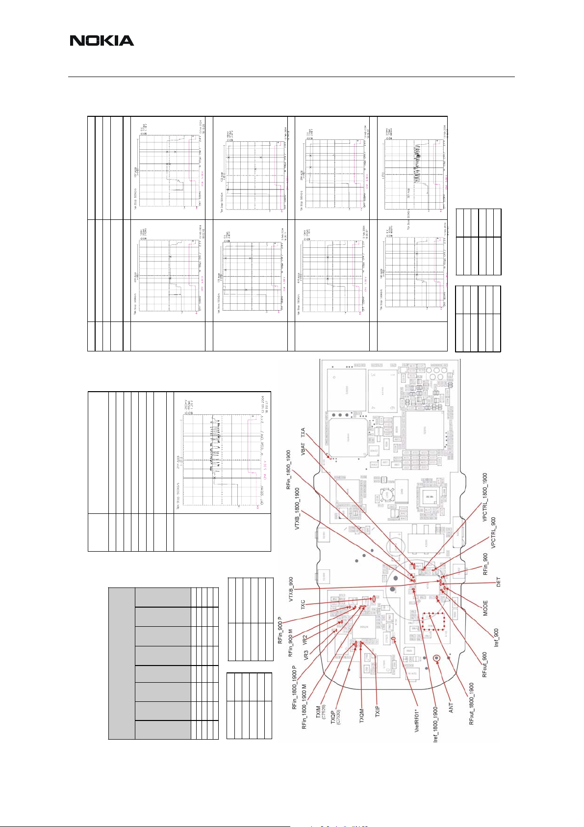
DC Supply Voltage Check
For a quick check of DC power supplies, refer to the diagram below. The RF power supplies
are generated in the UEM and can be measured either in the Small Signal Chamber or in the
Base Band Chamber.
The UEM output voltages can be measured at the respective resistors' / capacitors' pads
marked below in brackets, e.g. < C1234 >.
UEM
< C7516 >
< C7510 >
< R7516 >
< C7519 >
< C7517 >
VR1
VR2
VR3
VR4
VR5
4.75 V [ 4.6V ... 4.9V ]
charge pump (VCP)
2.78 V [ 2.70V ... 2.86V ]
Tx modulator (Vcc_ModOut)
TX buffer & EDGE ALCs (VRF_TX)
2.78 V [ 2.70V ... 2.86V ]
VCTCXO (+VCC)
digital interface (VDIG)
2.78 V [ 2.70V ... 2.86V ]
Rx Front End (VRF_RX)
Bias & Rx CH filters (VF_RX)
RF controls (VPAB_VLNA)
2.78 V [ 2.70V ... 2.86V ]
PLL prescaler (VPRE)
phasing dividers of Rx (VLO)
< C7521 >
< C7500 >
< R7511/C7516 >
< R2901/C2901 >
AND
VR6
VR7
V
refRF01
V
refRF02
2.78 V [ 2.70V ... 2.86V ]
2.78 V [ 2.70V ... 2.86V ]
16 mA [max. 20 mA]
1.35 V [ 1.32V ... 1.38V ]
100 uA
1.35 V [ 1.32V ... 1.38V ]
100 uA
BB buffer (VDIG)
VCO (VCC_VCO)
bias reference (VB_EXT)
bias reference
(RXIINN, RXQINN)
< R2900/C2900 >
VBAT
Issue 1 04/2005 COMPANY CONFIDENTIAL 39
Copyright © 2005 Nokia. All Rights Reserved.
2.7 V [ 2.95V ... 4.7V ]
Triple band PA
Page 40

RM-94
Nokia Customer Care 6(b) - RF Troubleshooting
This page has been intentionally left blank.
40 COMPANY CONFIDENTIAL Issue 1 04/2005
Copyright © 2005 Nokia. All Rights Reserved.
Page 41

Nokia Customer Care
Appendix 6A: Test Point s
Issue 1 04/2005 COMPANY CONFIDENTIAL
Copyright © 2005 Nokia. All Rights Reserved.
Page 42

RM-94
Nokia Customer Care Appendix 6A: Test Points
■ Receiver test points
V R 6
V R 4
B u r s t
C o n t in u o u s
o r
L N A B _ P *
T e s t p o i n t
B a n d G S M 9 0 0
A c t i v e U n i t R X
O p e r a t i o n M o d e
R X / T X C h a n n e l 3 7
D C L e v e l 2 . 8 V
T e s t p o i n t
B a n d G S M 1 9 0 0
A c t i v e U n i t R X
O p e r a t i o n M o d e C o n t i n u o u s
R X / T X C h a n n e l 6 6 1
B u r s t
C o n t in u o u s
T e s t p o i n t
B a n d G S M 9 0 0
A c t i v e U n i t R X
O p e r a t i o n M o d e
R x 3
L N A _ P *
o r
T e s t p o i n t
B a n d G S M 1 9 0 0
A c t i v e U n i t R X
O p e r a t i o n M o d e C o n t i n u o u s
R X / T X C h a n n e l 3 7
D C L e v e l 2 . 8 V
R X / T X C h a n n e l 6 6 1
2 . 5 d B
P r e f
T y p .
2 . 5 V
A G C : 1 4
D C L e v e l
T y p .
1 . 8 V
0 V
A G C : 4
D C L e v e l
A G C : 5
D C L e v e l
B u r s t
V r e f R F 0 1 *
C o n t in u o u s o r
T e s t p o i n t
B a n d G S M 9 0 0
A c t i v e U n i t R X
O p e r a t i o n M o d e
R X / T X C h a n n e l 3 7
D C L e v e l 1 . 3 5 V
1 ) V r e f R F 0 2 *
T e s t p o i n t s
B u r s t
C o n t i n u o u s o r
2 ) V r e f R F 0 2 * *
B a n d G S M 9 0 0
A c t i v e U n i t R X
O p e r a t i o n M o d e
R X / T X C h a n n e l 3 7
D C L e v e l 1 . 3 5 V
O U T - Z 7 8 0 1
T e s t p o i n t
B a n d G S M 1 9 0 0
A c t i v e U n i t R X
O p e r a t i o n M o d e C o n t i n u o u s
R X / T X C h a n n e l 6 6 1
O U T - V 7 8 0 0
T e s t p o i n t
B a n d G S M 1 9 0 0
A c t i v e U n i t R X
O p e r a t i o n M o d e C o n t i n u o u s
R X / T X C h a n n e l 6 6 1
V r e f R F 0 2 *
R 2 9 0 1 / C 2 9 0 1
V r e f R F 0 2 * *
R 2 9 0 0 / C 2 9 0 0
1 ) I N P _ P _ R X
2 ) I N M _ P _ R X
P r e f - 3 . 5 d B
A G C 1 4
I n p u t P o w e r 6 0 d B m
I n p u t F r e q u e n c y 1 9 6 0 . 0 6 7 7 1 M H z
P r o b e d P o w e r
P r e f + 1 4 d B
A G C 1 4
I n p u t P o w e r 6 0 d B m
I n p u t F r e q u e n c y 1 9 6 0 . 0 6 7 7 1 M H z
P r o b e d P o w e r
P r e f - 6 . 5 d B
T e s t p o i n t
B a n d G S M 1 9 0 0
A c t i v e U n i t R X
O p e r a t i o n M o d e C o n t i n u o u s
R X / T X C h a n n e l 6 6 1
A G C 1 4
I n p u t P o w e r 6 0 d B m
I n p u t F r e q u e n c y 1 9 6 0 . 0 6 7 7 1 M H z
P r o b e d P o w e r
2 . 0 d B
R x 2
T e s t p o i n t
B a n d G S M 1 8 0 0
A c t i v e U n i t R X
O p e r a t i o n M o d e C o n t i n u o u s
R X / T X C h a n n e l 7 0 0
R x 1
T e s t p o i n t
B a n d G S M 8 5 0 / 9 0 0
A c t i v e U n i t R X
O p e r a t i o n M o d e C o n t i n u o u s
R X / T X C h a n n e l 3 7
P r e f
A G C 1 4
I n p u t P o w e r 6 0 d B m
I n p u t F r e q u e n c y 1 8 4 2 . 8 6 7 7 1 M H z
P r o b e d P o w e r
1 . 5 . 0 d B
P r e f
A G C 1 4
I n p u t P o w e r 6 0 d B m
I n p u t F r e q u e n c y 9 4 2 . 4 6 7 7 1 M H z
P r o b e d P o w e r
L a y o u t : 1 c n a _ 4 1 ( B u i l d 4 . 0 )
t y p . 6 3 d B m
P r e f ( d B m )
t y p . 6 3 d B m
P r e f ( d B m )
t y p . 6 3 d B m
A N T ( A n t e n n a F e e d )
R e c e i v e r T e s t P o i n t s ( 1 / 2 )
T e s t p o i n t
B a n d G S M 9 0 0 G S M 1 8 0 0 G S M 1 9 0 0
A c t i v e U n i t R X
O p e r a t i o n M o d e C o n t i n u o u s
R X / T X C h a n n e l 3 7 7 0 0 6 6 1
P r e f ( d B m )
w i t h
A G C 1 4
I n p u t P o w e r 6 0 d B m 6 0 d B m 6 0 d B m
I n p u t F r e q u e n c y 9 4 2 . 4 6 7 7 1 M H z 1 8 4 2 . 8 6 7 7 1 M H z 1 9 6 0 . 0 6 7 7 1 M H z
P r o b e d P o w e r
( e . g . m e a s u r e d
r e s i s t iv e p r o b e ,r e f . t o
L 7 8 0 7 / C 7 8 0 6
I N M _ P _ R X
L 7 8 0 7 / C 7 8 0 5
I N P _ P _ R X
L 7 8 0 3
I N P _ D _ R X
L 7 8 0 2
I N M _ D _ R X
L 7 8 0 5
L N A B _ P *
R 7 8 0 1 / C 7 8 0 3
V C 3
V A N T _ 1
V C 1
V A N T _ 2
V C 2
V A N T _ 3
I N M _ G _ R X
L 7 8 0 4
I N P _ G _ R X
L 7 8 0 0 / C 7 8 0 1
O U T - Z 7 8 0 1
V R 6
V R 4
c h a p t e r 5 . 2 )
C 7 5 2 1
C 7 5 1 9
V r e f R F 0 1 *
R 7 5 1 1 / C 7 5 2 4
O U T - V 7 8 0 0
L 7 8 0 1 / C 7 8 0 4 / R 7 8 0 2
R x 3
L N A _ P *
R 7 8 0 0 / C 7 8 0 0
V A N T _ 1 , 2 , 3
T e s t p o i n t
R x 2
( G S M 1 9 0 0 )
( G S M 1 8 0 0 )
( V C 3 )
V A N T _ 3
( V C 1 )
V A N T _ 2
( V C 3 )
V A N T _ 1
B a n d G S M 9 0 0
A c t i v e U n i t R X [ T X ]
O p e r a t i o n M o d e C o n t i n u o u s
R X / T X C h a n n e l 3 7
T e s t p o i n t s
A N T
R x 1
( G S M 8 5 0 / 9 0 0 )
V A N T _ 1 , 2 , 3
T e s t p o i n t
B a n d G S M 1 8 0 0
D C L e v e l 0 V [ 2 . 6 V ] 0 V [ 0 V ] 0 V [ 2 . 6 V ]
A c t i v e U n i t R X [ T X ]
T e s t p o i n t s
B a n d G S M 1 9 0 0
A c t i v e U n i t R X
O p e r a t i o n M o d e C o n t i n u o u s
R X / T X C h a n n e l 6 6 1
A G C 1 4
I n p u t P o w e r 6 0 d B m
I n p u t F r e q u e n c y 1 9 6 0 . 0 6 7 7 1 M H z
P r o b e d P o w e r
D C L e v e l 1 . 6 V
1 ) I N P _ D _ R X
2 ) I N M _ D _ R X
T e s t p o i n t s
B a n d G S M 1 8 0 0
A c t i v e U n i t R X
O p e r a t i o n M o d e C o n t i n u o u s
R X / T X C h a n n e l 7 0 0
G N D
a n d p i n s
( G R O U N D )
m e t a l s h i e l d i n g
1 ) I N P _ G _ R X
2 ) I N M _ G _ R X
T e s t p o i n t s
B a n d G S M 9 0 0
A c t i v e U n i t R X
O p e r a t i o n M o d e C o n t i n u o u s
R X / T X C h a n n e l 3 7
( V C 3 )
V A N T _ 3
( V C 1 )
V A N T _ 2
V A N T _ 1
O p e r a t i o n M o d e C o n t i n u o u s
R X / T X C h a n n e l 7 0 0
T e s t p o i n t s
V A N T _ 1 , 2 , 3
( V C 3 )
D C L e v e l 0 V [ 0 V ] 0 V [ 2 . 6 V ] 0 V [ 2 . 6 V ]
T e s t p o i n t
B a n d G S M 1 9 0 0
P r e f 6 d B
A G C 1 4
I n p u t P o w e r 6 0 d B m
I n p u t F r e q u e n c y 1 8 4 2 . 8 6 7 7 1 M H z
P r o b e d P o w e r
D C L e v e l T y p . 1 . 6 V
P r e f 3 . 5 d B
A G C 1 4
I n p u t P o w e r 6 0 d B m
I n p u t F r e q u e n c y 9 4 2 . 4 6 7 7 1 M H z
P r o b e d P o w e r
D C L e v e l T y p . 1 . 6 V
( V C 3 )
V A N T _ 3
( V C 1 )
V A N T _ 2
( V C 3 )
V A N T _ 1
A c t i v e U n i t R X [ T X ]
O p e r a t i o n M o d e C o n t i n u o u s
R X / T X C h a n n e l 6 6 1
T e s t p o i n t s
D C L e v e l 0 V [ 0 V ] 0 V [ 2 . 6 V ] 2 . 6 V [ 2 . 6 V ]
42 COMPANY CONFIDENTIAL Issue 1 04/2005
Copyright © 2005 Nokia. All Rights Reserved.
Page 43

RM-94
Appendix 6A: Test Points Nokia Customer Care
1 ) R X I
2 ) R X Q
T e s t p o i n t s
B a n d G S M 9 0 0 o r G S M 1 8 0 0 o r G S M 1 9 0 0
A c t i v e U n i t R X
O p e r a t i o n M o d e C o n t i n u o u s
R X / T X C h a n n e l 3 7 o r 7 0 0 o r 6 6 1
1 ) C M _ F _ I
2 ) C M _ F _ Q
T e s t p o i n t s
B a n d G S M 9 0 0 o r G S M 1 8 0 0 o r G S M 1 9 0 0
A c t i v e U n i t R X
1 . 4 V p p
A G C 1 0
I n p u t P o w e r 6 0 d B m
I n p u t F r e q u e n c y 9 4 2 . 4 6 7 7 1 , 1 8 4 2 . 8 6 7 7 1 o r 1 9 6 0 . 0 6 7 7 1 M H z
S i g n a l
A m p l i t u d e
D C O f f s e t 1 . 2 8 V d c
F r e q u e n c y 6 7 k H z
G r a p h
( t y p i c a l f o r a l l
T P s a n d b a n d s )
A p p r o x . 1 . 7 5 V p p
O p e r a t i o n M o d e B u r s t
R X / T X C h a n n e l 3 7 o r 7 0 0 o r 6 6 1
A G C 1 0
I n p u t P o w e r 6 0 d B m
I n p u t F r e q u e n c y 9 4 2 . 4 6 7 7 1 , 1 8 4 2 . 8 6 7 7 1 o r 1 9 6 0 . 0 6 7 7 1 M H z
S i g n a l
A m p l i t u d e
G r a p h
( t y p i c a l f o r b o t h
T P s a n d a l l
b a n d s )
1 ) C M _ D T O S _ I
2 ) C M _ D T O S _ Q
T e s t p o i n t s
B a n d G S M 9 0 0 o r G S M 1 8 0 0 o r G S M 1 9 0 0
A c t i v e U n i t R X
O p e r a t i o n M o d e B u r s t
R X / T X C h a n n e l 3 7 o r 7 0 0 o r 6 6 1
A p p r o x . 2 V p p
A G C 1 4
I n p u t P o w e r 6 0 d B m
I n p u t F r e q u e n c y 9 4 2 . 4 6 7 7 1 , 1 8 4 2 . 8 6 7 7 1 o r 1 9 6 0 . 0 6 7 7 1 M H z
S i g n a l
A m p l i t u d e
G r a p h
( t y p i c a l f o r b o t h
T P s a n d a l l
b a n d s )
Issue 1 04/2005 COMPANY CONFIDENTIAL 43
Copyright © 2005 Nokia. All Rights Reserved.
Page 44
RM-94
Nokia Customer Care Appendix 6A: Test Points
■ T ransmitter test points
VR3
Testpoint
Band GSM900
Active Unit TX
Operation Mode Burst
RX/TX Channel 37
DC Level 2.8V
GMSK ( EDGE = OFF ) 8-PSK ( EDGE = ON )
Burst Burst
Modulation
Band GSM 850 or 900 or 1800 or 1900 GSM 850 or 900 o r 1800 or 1900
Active Unit TX TX
Operation
Mode
Test point TXC TXC
Graph
e.g.
GSM900 PL10
TXIP (R713/1)
TXIM (R713/3)
TXIP (R713/7)
TXQM (R713/5))
Testpoints
Band GSM 850 or 900 or GSM1800 or GSM1900
Active Unit TX
Operation Mode Burst
RX/TX Channel 190 or 37 or 700 o r 661
Tx Data Type Random
Tx Power Level any
Tx2
Tx1
Rx3
Transmitter Test Points (1/3)
Rx2
Rx1
_1
VANT
Test points: RFout_900 and RFout_1800/1900
Matrix Antenna Switch Module Z7800
_3
VANT
_2
VANT
RFout
RFout
520mVpp
Signal
Amplitude
/1900
_1800
_900
VC3
VC2
VC1
[Volt]
Test point VTXB_900 VTXB_900
Graph e.g.
GSM900 PL10
Test point VPctrl_900 VPctrl_900
Graph
e.g.
GSM900 PL10
Test point VDET
VREF01
Testpoint
Band GSM900
Active Unit TX
Operation Mode Burst
RX/TX Channel 37
DC Level 1.35V
Layout: 1cna_41 (Build 4.0)
TXA
VPCTRL_1800_1900
VBAT
DC Offset 1. 2Vdc
Graph
(typical for all
TPs and bands)
Tx
1800
GSM
/1900
Tx
850
/900
GSM
Rx
1900
GSM
X
Rx
1800
GSM
Rx
850
/900
GSM
[Volt]
[Volt]
0 0 0 X
0 0 0
VR2 (C7512)
X
X
X
Testpoint
Band GSM900/1800/1900
VBAT
0 2.6 2.6
0 2.6 0
2.6 2.6 0
Testpoint
Band GSM900
Active Unit TX
Active Unit TX
Operation Mode Burst
RX/TX Channel 37
DC Level 2.8V
Operation Mode Burst
RX/TX Channel 37
DC Level Typ. 3.6V
RFin_1800_1900
VTXB_1800_1900
VTXB_900
VR3
RFin_900 P
RFin_1800_1900 P
TXC
RFin_900 M
RFin_1800_1900 M
VR2
TXQP
TXQM
(C7530)
TXIP
TXIM
(C7529)
VrefRF01*
VPCTRL_900
RFin_900
MODE
Iref_900
Iref_1800_1900 DETRFout_900
RFout_1800_1900
ANT
44 COMPANY CONFIDENTIAL Issue 1 04/2005
Copyright © 2005 Nokia. All Rights Reserved.
Page 45

RM-94
Appendix 6A: Test Points Nokia Customer Care
+ d B m
+ 2 d B m
+ d B m
1 . R F i n _ 9 0 0 P
2 . R F i n _ 9 0 0 M
T e s t p o i n t
B a n d G S M 8 5 0 o r 9 0 0
A c t i v e U n i t T X
O p e r a t i o n M o d e B u r s t
M o d u l a t i o n G M S K ( E d g e = o f f )
R X / T X C h a n n e l 1 9 0 o r 3 7
T x P o w e r L e v e l 1 0
T x D a t a T y p e A l l 1
P o w e r @ 5 0 O h m s
P o w e r @ p r o b e
+ 2 d B m
+ d B m
R F i n _ 9 0 0
1 . R F i n _ 1 8 0 0 _ 1 9 0 0 P
2 . R F i n _ 1 8 0 0 _ 1 9 0 0 M
T e s t p o i n t
B a n d G S M 1 8 0 0 o r 1 9 0 0
A c t i v e U n i t T X
O p e r a t i o n M o d e B u r s t
M o d u l a t i o n G M S K ( E d g e = o f f )
R F i n _ 1 8 0 0 _ 1 9 0 0
L a y o u t : 1 c n a _ 4 1 ( B u i l d 4 . 0 )
V P C T R L _ 1 8 0 0 _ 1 9 0 0
T X A
T e s t p o i n t
B a n d G S M 8 5 0 o r 9 0 0
A c t i v e U n i t T X
O p e r a t i o n M o d e B u r s t
M o d u l a t i o n G M S K ( E d g e = o f f )
R X / T X C h a n n e l 1 9 0 o r 3 7
T x P o w e r L e v e l 1 0
T x D a t a T y p e A l l 1
P o w e r @ 5 0 O h m s
P o w e r @ p r o b e
V B A T
T e s t p o i n t
B a n d G S M 1 8 0 0 o r 1 9 0 0
A c t i v e U n i t T X
O p e r a t i o n M o d e B u r s t
M o d u l a t i o n G M S K ( E d g e = o f f )
V P C T R L _ 9 0 0
+ 0 d B m
R X / T X C h a n n e l 7 0 0 o r 6 6 1
T x P o w e r L e v e l 5
T x D a t a T y p e A l l 1
P o w e r @ 5 0 O h m s
P o w e r @ p r o b e
+ 2 d B m
+ d B m
R X / T X C h a n n e l 7 0 0 o r 6 6 1
T x P o w e r L e v e l 5
T x D a t a T y p e A l l 1
P o w e r @ 5 0 O h m s
P o w e r @ p r o b e
R F i n _ 1 8 0 0 _ 1 9 0 0
+ d B m
R F o u t _ 9 0 0
+ 2 4 . 3 d B m
R F i n _ 9 0 0
R F o u t _ 1 8 0 0 _ 1 9 0 0
M O D E
I r e f _ 9 0 0
+ d B m
+ 2 1 . 6 d B m
V T X B _ 1 8 0 0 _ 1 9 0 0
T e s t p o i n t
B a n d G S M 8 5 0 o r 9 0 0
A c t i v e U n i t T X
O p e r a t i o n M o d e B u r s t
M o d u l a t i o n G M S K ( E d g e = o f f )
R X / T X C h a n n e l 1 9 0 o r 3 7
T x P o w e r L e v e l 1 0
T x D a t a T y p e A l l 1
P o w e r @ 5 0 O h m s
P o w e r @ p r o b e
V T X B _ 9 0 0
T X C
T e s t p o i n t
B a n d G S M 1 8 0 0 o r 1 9 0 0
A c t i v e U n i t T X
O p e r a t i o n M o d e B u r s t
M o d u l a t i o n G M S K ( E d g e = o f f )
R X / T X C h a n n e l 7 0 0 o r 6 6 1
T x P o w e r L e v e l 5
T x D a t a T y p e A l l 1
P o w e r @ 5 0 O h m s
P o w e r @ p r o b e
I r e f _ 1 8 0 0 _ 1 9 0 0 D E TR F o u t _ 9 0 0
V R 3
+ 2 0 d B m
+ 2 3 d B m
+ d B m
R F i n _ 9 0 0 P
A N T
R F i n _ 9 0 0 M
A N T
+ d B m
R F o u t _ 1 8 0 0 _ 1 9 0 0
T e s t p o i n t
B a n d G S M 8 5 0 o r 9 0 0
A c t i v e U n i t T X
O p e r a t i o n M o d e B u r s t
M o d u l a t i o n G M S K ( E d g e = o f f )
R X / T X C h a n n e l 1 9 0 o r 3 7
T x P o w e r L e v e l 1 0
T x D a t a T y p e A l l 1
P o w e r @ 5 0 O h m s
P o w e r @ p r o b e
V R 2
T X Q P
T X Q M
R F i n _ 1 8 0 0 _ 1 9 0 0 P
R F i n _ 1 8 0 0 _ 1 9 0 0 M
( C 7 5 3 0 )
T X I P
T X I M
( C 7 5 2 9 )
V r e f R F 0 1 *
A N T
T e s t p o i n t
B a n d G S M 1 8 0 0 o r 1 9 0 0
A c t i v e U n i t T X
O p e r a t i o n M o d e B u r s t
M o d u l a t i o n G M S K ( E d g e = o f f )
R X / T X C h a n n e l 7 0 0 o r 6 6 1
T x P o w e r L e v e l 5
T x D a t a T y p e A l l 1
P o w e r @ 5 0 O h m s
P o w e r @ p r o b e
e 5 0 O h m s p o w e r m e a s u r e m e n t .
R F @ T e s t - J i g
T y p . + 2 3 d B m
R F @ T e s t - J i g
T y p . + 2 0 d B m
T e s t p o i n t
B a n d G S M 8 5 0 o r 9 0 0
A c t i v e U n i t T X
O p e r a t i o n M o d e B u r s t
M o d u l a t i o n G M S K ( E d g e = o f f )
R X / T X C h a n n e l 1 9 0 o r 3 7
T x P o w e r L e v e l 1 0
T x D a t a T y p e A l l 1
P o w e r @ 5 0 O h m
L o s s e s o f j i g c o m p e n s a t e d
m e a s u r e m e n t w i t h t h
P o w e r m e a s u r e m e n t s a t t h e t e s t p o i n t s b y m e a n s o f a p r o b e w i t h 4 7 0 ( ! ) O h m s a t t h e p e a k o n l y . G a i n s o r l o s s e s o f t h e k e y c o m p o n e n t s d e t e c t e d w i t h t h e p r o b e s h a l l b e c o m p a r a b l e t o t h e
T e s t p o i n t
B a n d G S M 1 8 0 0 o r 1 9 0 0
A c t i v e U n i t T X
O p e r a t i o n M o d e B u r s t
M o d u l a t i o n G M S K ( E d g e = o f f )
R X / T X C h a n n e l 7 0 0 o r 6 6 1
T x P o w e r L e v e l 5
T x D a t a T y p e A l l 1
P o w e r @ 5 0 O h m s
L o s s e s o f j i g c o m p e n s a t e d
Issue 1 04/2005 COMPANY CONFIDENTIAL 45
Copyright © 2005 Nokia. All Rights Reserved.
Page 46

RM-94
Nokia Customer Care Appendix 6A: Test Points
- 1 5 - 8 d B m
1 . R F i n _ 9 0 0 P
2 . R F i n _ 9 0 0 M
T e s t p o i n t
B a n d G S M 8 5 0 o r 9 0 0
A c t i v e U n i t T X
O p e r a t i o n M o d e B u r s t
M o d u l a t i o n 8 - P S K ( E d g e = o n )
R X / T X C h a n n e l 1 9 0 o r 3 7
R F i n _ 9 0 0
d B m
1 . R F i n _ 1 8 0 0 _ 1 9 0 0 P
B O M 1 , B O M 2 , B O M 2 b
I r e f _ 9 0 0
T x P o w e r L e v e l 1 0
T x D a t a T y p e A l l 1
P o w e r @ 5 0 O h m s
P o w e r @ p r o b e
d B m
- 1 5 - 8 d B m
G S M 8 5 0 o r 9 0 0
T e s t p o i n t
B a n d
A c t i v e U n i t T X
O p e r a t i o n M o d e B u r s t
M o d u l a t i o n 8 - P S K ( E d g e = o n )
R X / T X C h a n n e l 1 9 0 o r 3 7
T x P o w e r L e v e l 1 0
T x D a t a T y p e A l l 1
U s e s a m e t e s t p o i n t
I r e f _ 9 0 0 f o r h i g h e r G S M
I r e f _ 1 8 0 0 _ 1 9 0 0 ( B O M 1 )
I r e f _ 9 0 0 ( B O M 2 , B O M 2 b )
b a n d s i n c a s e o f B O M 2
a n d B O M 2 b !
G S M 1 8 0 0 o r 1 9 0 0
V o l t a g e 1 . 9 2 V ( B u r s t )
T e s t p o i n t
R E M A R K
B a n d
A c t i v e U n i t T X
O p e r a t i o n M o d e B u r s t
M o d u l a t i o n 8 - P S K ( E d g e = o n )
R X / T X C h a n n e l 7 0 0 o r 6 6 1
T x P o w e r L e v e l 1 0
T x D a t a T y p e A l l 1
V o l t a g e 2 . 0 V ( B u r s t )
2 . R F i n _ 1 8 0 0 _ 1 9 0 0 M
T e s t p o i n t
B a n d G S M 1 8 0 0 o r 1 9 0 0
A c t i v e U n i t T X
O p e r a t i o n M o d e B u r s t
M o d u l a t i o n 8 - P S K ( E d g e = o n )
R X / T X C h a n n e l 7 0 0 o r 6 6 1
R F i n _ 1 8 0 0 _ 1 9 0 0
L a y o u t : 1 c n a _ 4 1 ( B u i l d 4 . 0 )
V P C T R L _ 1 8 0 0 _ 1 9 0 0
T e s t p o i n t
B a n d G S M 8 5 0 o r 9 0 0
A c t i v e U n i t T X
O p e r a t i o n M o d e B u r s t
M o d u l a t i o n 8 - P S K ( E d g e = o n )
R X / T X C h a n n e l 1 9 0 o r 3 7
T x P o w e r L e v e l 1 0
T x D a t a T y p e A l l 1
P o w e r @ 5 0 O h m s
P o w e r @ p r o b e
T X A
T e s t p o i n t
B a n d G S M 1 8 0 0 o r 1 9 0 0
A c t i v e U n i t T X
O p e r a t i o n M o d e B u r s t
M o d u l a t i o n 8 - P S K ( E d g e = o n )
d B m
- 1 8 - 1 0 d B m
T x P o w e r L e v e l 5
T x D a t a T y p e A l l 1
P o w e r @ 5 0 O h m s
P o w e r @ p r o b e
- 1 6 - 8 d B m
d B m
R X / T X C h a n n e l 7 0 0 o r 6 6 1
T x P o w e r L e v e l 5
T x D a t a T y p e A l l 1
P o w e r @ 5 0 O h m s
P o w e r @ p r o b e
V B A T
V P C T R L _ 9 0 0
+ 2 5 . 8 d B m
R F o u t _ 9 0 0
T e s t p o i n t
B a n d G S M 8 5 0 o r 9 0 0
A c t i v e U n i t T X
O p e r a t i o n M o d e B u r s t
M o d u l a t i o n 8 - P S K ( E d g e = o n )
R X / T X C h a n n e l 1 9 0 o r 3 7
+ d B m
T x P o w e r L e v e l 1 0
T x D a t a T y p e A l l 1
P o w e r @ 5 0 O h m s
P o w e r @ p r o b e
R F i n _ 1 8 0 0 _ 1 9 0 0
V T X B _ 1 8 0 0 _ 1 9 0 0
V T X B _ 9 0 0
T X C
V R 3
+ 2 4 . 5 d B m
A N T
T e s t p o i n t
B a n d G S M 8 5 0 o r 9 0 0
A c t i v e U n i t T X
O p e r a t i o n M o d e B u r s t
M o d u l a t i o n 8 - P S K ( E d g e = o n )
R X / T X C h a n n e l 1 9 0 o r 3 7
+ d B m
R F i n _ 9 0 0 P
T x P o w e r L e v e l 1 0
T x D a t a T y p e A l l 1
P o w e r @ 5 0 O h m s
P o w e r @ p r o b e
R F i n _ 9 0 0 M
V R 2
T X Q P
T X Q M
R F i n _ 1 8 0 0 _ 1 9 0 0 P
R F i n _ 1 8 0 0 _ 1 9 0 0 M
( C 7 5 3 0 )
T X I P
T X I M
( C 7 5 2 9 )
V r e f R F 0 1 *
R F i n _ 9 0 0
+ 2 3 . 1 d B m
R F o u t _ 1 8 0 0 _ 1 9 0 0
M O D E
I r e f _ 9 0 0
T e s t p o i n t
B a n d G S M 1 8 0 0 o r 1 9 0 0
A c t i v e U n i t T X
O p e r a t i o n M o d e B u r s t
M o d u l a t i o n 8 - P S K ( E d g e = o n )
R X / T X C h a n n e l 7 0 0 o r 6 6 1
+ d B m
T x P o w e r L e v e l 5
T x D a t a T y p e A l l 1
P o w e r @ 5 0 O h m s
P o w e r @ p r o b e
I r e f _ 1 8 0 0 _ 1 9 0 0 D E TR F o u t _ 9 0 0
+ d B m
A N T
R F o u t _ 1 8 0 0 _ 1 9 0 0
T e s t p o i n t
B a n d G S M 1 8 0 0 o r 1 9 0 0
A c t i v e U n i t T X
O p e r a t i o n M o d e B u r s t
M o d u l a t i o n 8 - P S K ( E d g e = o n )
+ 2 1 . 5 d B m
R X / T X C h a n n e l 7 0 0 o r 6 6 1
T x P o w e r L e v e l 5
T x D a t a T y p e A l l 1
P o w e r @ 5 0 O h m s
P o w e r @ p r o b e
A N T
e 5 0 O h m s p o w e r m e a s u r e m e n t .
R F @ T e s t - J i g
T e s t p o i n t
B a n d G S M 8 5 0 o r 9 0 0
A c t i v e U n i t T X
O p e r a t i o n M o d e B u r s t
m e a s u r e m e n t w i t h t h
P o w e r m e a s u r e m e n t s a t t h e t e s t p o i n t s b y m e a n s o f a p r o b e w i t h 4 7 0 ( ! ) O h m s a t t h e p e a k o n l y . G a i n s o r l o s s e s o f t h e k e y c o m p o n e n t s d e t e c t e d w i t h t h e p r o b e s h a l l b e c o m p a r a b l e t o t h e
M o d u l a t i o n 8 - P S K ( E d g e = o n )
T y p . + 2 4 . 5 d B m
M O D E
R X / T X C h a n n e l 1 9 0 o r 3 7
T x P o w e r L e v e l 1 0
T x D a t a T y p e A l l 1
P o w e r @ 5 0 O h m s
L o s s e s o f j i g c o m p e n s a t e d
T e s t p o i n t
B a n d G S M 8 5 0 / 9 0 0 / 1 8 0 0 / 1 9 0 0
A c t i v e U n i t T X
O p e r a t i o n M o d e B u r s t
M o d u l a t i o n 8 - P S K ( E d g e = o n )
R X / T X C h a n n e l 1 9 0 o r 3 7 o r 7 0 0 o r 6 6 1
T x P o w e r L e v e l 1 0
T x D a t a T y p e A l l 1
V o l t a g e 1 . 9 6 V ( B u r s t )
R F @ T e s t - J i g
T e s t p o i n t
B a n d G S M 1 8 0 0 o r 1 9 0 0
A c t i v e U n i t T X
O p e r a t i o n M o d e B u r s t
M o d u l a t i o n 8 - P S K ( E d g e = o n )
+ 2 1 . 5 d B m
R X / T X C h a n n e l 7 0 0 o r 6 6 1
T x P o w e r L e v e l 5
T x D a t a T y p e A l l 1
P o w e r @ 5 0 O h m s
L o s s e s o f j i g c o m p e n s a t e d
46 COMPANY CONFIDENTIAL Issue 1 04/2005
Copyright © 2005 Nokia. All Rights Reserved.
Page 47

RM-94
Appendix 6A: Test Points Nokia Customer Care
■ Synthesizer test points
l i f i e r w i l l b e d e s t r o y e d .
M e a s u r e d u s i n g t h e s p e c i a l p r o b e w i t h
~ 0 d B m ~ 0 d B m ~ 0 d B m
c a p a c i t i v e c o u p l i n g . N o e x a c t p o w e r
T a k e c a r e t o s e l e c t t h e h i g h e s t P C L 1 5 i f
a c t i v a t i n g T X C o n t i n u o u s m o d e , o t h e r w i s e
t h e p o w e r a m p
T e s t p o i n t A F C ( V c o f V C T C X O )
B a n d d e f a u l t
A c t i v e U n i t R X
O p e r a t i o n M o d e C o n t i n u o u s
R X / T X C h a n n e l a n y
A F C ( v a l u e ) - 1 0 2 4 1 5 0 1 0 2 3
A F C v o l t a g e 0 . 1 V 1 . 4 V 2 . 5 V
T e s t p o i n t V c o f V C O
B a n d G S M 1 8 0 0 G S M 1 9 0 0 G S M 1 9 0 0
A c t i v e U n i t T X T X R X
O p e r a t i o n M o d e C o n t i n u o u s
R X / T X C h a n n e l 5 1 2 5 1 2 8 1 0
F r e q u e n c y 3 4 2 0 . 4 M H z 3 7 0 0 . 4 M H z 3 9 7 9 . 6 M H z
D C L e v e l ~ 1 . 3 V ~ 2 . 5 V ~ 3 . 6 V
T e s t p o i n t V R 1 V r e f R F 0 1 V r e f R F 0 2
B a n d d e f a u l t ( G S M 9 0 0 o r G S M 8 5 0 )
A c t i v e U n i t R x
O p e r a t i o n M o d e B u r s t o r C o n t i n u o u s
R X / T X C h a n n e l d e f a u l t
D C L e v e l 4 . 7 6 1 . 3 5 V 1 . 3 5 V
T e s t p o i n t V R 3 V R 5 V R 7
B a n d d e f a u l t ( G S M 9 0 0 o r G S M 8 5 0 )
A c t i v e U n i t R x
O p e r a t i o n M o d e B u r s t o r C o n t i n u o u s
R X / T X C h a n n e l d e f a u l t
D C L e v e l 2 . 7 8 V 2 . 7 8 V 2 . 7 8 V
N o t e
( C 2 9 0 2 / R 2 9 0 2 )
R F C L K _ I
T e s t p o i n t V C O o u t
B a n d G S M 1 8 0 0 G S M 1 9 0 0 G S M 1 9 0 0
A c t i v e U n i t T X T X R X
O p e r a t i o n M o d e C o n t i n u o u s
R X / T X C h a n n e l 5 1 2 5 1 2 8 1 0
F r e q u e n c y 3 4 2 0 . 4 M H z 3 7 0 0 . 4 M H z 3 9 7 9 . 6 M H z
L e v e l
m e a s u r e m e n t p o s s i b l e .
( s p e c . r a n g e =
N o t e s
- 3 . 5 + 2 . 5 d B m )
e r w i l l b e d e s t r o y e d .
T a k e c a r e t o s e l e c t t h e h i g h e s t P C L 1 5 i f
a c t i v a t i n g T X C o n t i n u o u s m o d e , o t h e r w i s e
t h e p o w e r a m p l i f i
R F B u s C l k , R F B u s D a t a , R F B u s E n a 1
T e s t p o i n t
B a n d d e f a u l t ( G S M 9 0 0 o r G S M 8 5 0 )
~ 2 V
R F B u s C l k ( J 1 0 0 1 )
A c t i v e U n i t R X
O p e r a t i o n M o d e B u r s t
R X / T X C h a n n e l d e f a u l t
S i g n a l
A m p l i t u d e
G r a p h
R F B u s C l k
R F B u s D a t a R F B u s E n a 1
R F B u s D a t a ( J 1 0 0 3 )
R F B u s E n a 1 ( J 1 0 0 2 )
V R 1 V R 5
V R 3
2 6 M H z
V C T C X O o u t
L a y o u t : 1 c n a _ 4 1 ( B u i l d 4 . 0 )
V C T C X O o u t ( R E F C L K )
T e s t p o i n t
B a n d d e f a u l t
S y n t h e s i z e r T e s t P o i n t s ( 1 / 1 )
8 8 0 m V p p
A c t i v e U n i t R X
O p e r a t i o n M o d e C o n t i n u o u s
R X / T X C h a n n e l d e f a u l t
S i g n a l
A m p l i t u d e
D C O f f s e t 1 . 5 V
F r e q u e n c y 2 6 M H z
G r a p h
m e a s u r e d w i t h p a s s i v e p r o b e 1 0 x , 1 0 M o h m / 8 p F , A C c o u p l e d )
A F C ( G 7 5 0 1 )
V c o f V C T C X O
V c o f V C O
( C 7 5 0 3 )
V C O o u t
3 . . 4 . 5 G H z
V r e f R F 0 1
V R 7 ( C 7 5 0 0 )
Issue 1 04/2005 COMPANY CONFIDENTIAL 47
Copyright © 2005 Nokia. All Rights Reserved.
Page 48

RM-94
Nokia Customer Care Appendix 6A: Test Points
This page has been intentionally left blank.
48 COMPANY CONFIDENTIAL Issue 1 04/2005
Copyright © 2005 Nokia. All Rights Reserved.
 Loading...