

Page 1

Nokia Customer Care
7 - System Module
Issue 1 04/2005 COMPANY CONFIDENTIAL
Copyright © 2005 Nokia. All Rights Reserved.
Page 2

RM-94
Nokia Customer Care 7 - System Module
This page has been intentionally left blank
2 COMPANY CONFIDENTIAL Issue 1 04/2005
Copyright © 2005 Nokia. All Rights Reserved.
Page 3

RM-94
7 - System Module Nokia Customer Care
Table of Contents
Page No
Glossary of Terms............................................................................................... 5
Baseband.............................................................................................................8
Block diagram .................................................................................................... 9
Frequencies in baseband................................................................................. 11
PWB................................................................................................................. 11
Characteristics of the PWB ............................................................................11
Key components ............................................................................................11
Technical Specifications .................................................................................. 13
Baseband core................................................................................................. 13
UPP ................................................................................................................13
UEMEK ..........................................................................................................13
External SRAM and Flash ..............................................................................14
Energy management........................................................................................ 14
Modes of operation ........................................................................................14
No Supply ......................................................................................................14
Backup ...........................................................................................................14
Acting Dead ...................................................................................................14
Active .............................................................................................................15
Sleep Mode ....................................................................................................15
Charging ........................................................................................................15
Power distribution ............................................................................................ 15
DC characteristics............................................................................................ 16
Supply voltage ranges ...................................................................................16
Baseband regulators ......................................................................................17
Function Groups ............................................................................................... 18
Battery.............................................................................................................. 18
Audio................................................................................................................ 18
Internal microphone ....................................................................................... 18
Internal speaker ............................................................................................. 19
IHF speaker ...................................................................................................20
External audio ................................................................................................20
External microphone connection ....................................................................20
Headset connections .....................................................................................20
Test possibilities .............................................................................................20
Vibra................................................................................................................. 20
Test possibility ...............................................................................................21
LCD module..................................................................................................... 21
Characteristics ...............................................................................................21
LCD connector ...............................................................................................22
Test possibility ...............................................................................................23
Keypad............................................................................................................. 24
Test possibility ...............................................................................................24
Issue 1 04/2005 COMPANY CONFIDENTIAL 3
Copyright © 2005 Nokia. All Rights Reserved.
Page 4
RM-94
Nokia Customer Care 7 - System Module
Illumination....................................................................................................... 24
Test possibility ...............................................................................................25
SIM................................................................................................................... 25
Test possibility ...............................................................................................26
IR module......................................................................................................... 26
Interfaces ...........................................................................................................27
BB-RF interface ............................................................................................... 27
System connector interface ............................................................................. 27
System connector ..........................................................................................27
ACI .................................................................................................................28
FBUS .............................................................................................................28
VOUT .............................................................................................................28
DC plug ..........................................................................................................29
RF Module Description.....................................................................................30
General specifications of the transceiver......................................................... 31
Frequency concept .......................................................................................... 32
RF power supply configuration ........................................................................ 32
RF block diagram............................................................................................. 33
Antenna switch (TX/RX switch)........................................................................ 34
Receiver .........................................................................................................35
Transmitter .....................................................................................................35
Frequency synthesizer ...................................................................................35
Signal paths..................................................................................................... 36
Receiver signal paths .....................................................................................36
Transmitter signal paths .................................................................................38
Frequency synthesizer signals .......................................................................39
Printed Wiring Board ........................................................................................ 40
RF key component placement ......................................................................... 41
4 COMPANY CONFIDENTIAL Issue 1 04/2005
Copyright © 2005 Nokia. All Rights Reserved.
Page 5

RM-94
7 - System Module Nokia Customer Care
Glossary of Terms
ACI Accessory Control Interface
ADC Analogue to Digital Converter
AFC Automatic Frequency Control
ASIC Application Specific Integrated Circuit
ASM Antenna switch module
BB Baseband
BSI Battery Size Indicator
DCT4 Digital Core Technology, generation 4
DSP Digital Signal Processor
DUT Device under test
EDGE Enhanced Data Rates for Global Evolution
EGPRS Enhanced General Packed Radio Service
EMC Electro Magnetic Compatibility
ESD Electro Static Discharge
FCI Functional Cover Interface
FR Full Rate
GMSK Gaussian Minimum Shift Keying
GPRS General Packed Radio Service
GSM Global System for Mobile Communication
GSM900 GSM900 (channels 1 - 124)+extended GSM900
(channels 975 - 1023, 0)
HSCSD High Speed Circuit Switched Data
HW Hardware
IF Interface
IHF Integrated Hands Free
Issue 1 04/2005 COMPANY CONFIDENTIAL 5
Copyright © 2005 Nokia. All Rights Reserved.
Page 6

RM-94
Nokia Customer Care 7 - System Module
IMEI International Mobile Equipment Identity
I/O Input/Output
IR Infrared
IrDA Infrared Data Association
LCD Liquid Crystal Display
LED Light Emitting Diode
LDO Low Drop Out
LNA Low Noise Amplifier
LO Local Oscillator
MCU Micro Controller Unit
PA Power Amplifier
Phoenix SW tool of DCT4
PLL Phase Locked Loop
PWB Printed Wired Board
RF Radio Frequency
RTC Real Time Clock
RX Receiver
SA Spectrum analyzer
SIM Subscriber Identification Module
SW Software
TP Test point
TX Transmitter
UEMEK Universal Energy Management ASIC enhanced version
UI User Interface
UPP Universal Phone Processor
USB Universal Serial Bus
6 COMPANY CONFIDENTIAL Issue 1 04/2005
Copyright © 2005 Nokia. All Rights Reserved.
Page 7

RM-94
7 - System Module Nokia Customer Care
VBU
<COFF>
Back-up Battery Cut Off voltage (typical: 2.0 V)
VCO Voltage controlled oscillator
VCTCXO Voltage controlled temperature compensated oscillator
V
<MSTR+>
Master Reset Threshold (typical: 2.1 V)
8-PSK Phase Shift Keying with 8 states (Modulation scheme for EDGE/
GPRS)
Issue 1 04/2005 COMPANY CONFIDENTIAL 7
Copyright © 2005 Nokia. All Rights Reserved.
Page 8

RM-94
Nokia Customer Care 7 - System Module
Baseband
The RM-94 product is a DCT4.5 expression segment phone designed for the EGSM900,
GSM1800 and GSM1900 networks.
The HW has the following features:
• GPRS and HSCSD with EDGE in up to (2RX + 2TX) (MCS5), without EDGE also
in (3RX + 1TX) (MCS6)
• DCT4 with AMR and 16 MIDI tones
• 128/16 Mbit Combo memory
• Active display with 64k colours
• Battery BL-5B
• Illuminated XPress on grips
• PopPort
TM
interface
• 5-way navigation key with select
• FCI rear side (C-cover)
•Vibra
•IHF
The RM-94 BB is based on the DCT4/4.5 engine and is compatible to the PopPort
ries. The DCT4/4.5 engine consists basically of two ASICs. The UEMEK (Universal Energy
Management IC including voltage regulators, charge control and audio circuit s, audio IFH amplifier from DCT4.5) and the UPP (Universal Phone Processor including MCU, DSP and RAM
from DCT4).
TM
accesso-
8 COMPANY CONFIDENTIAL Issue 1 04/2005
Copyright © 2005 Nokia. All Rights Reserved.
Page 9
RM-94
7 - System Module Nokia Customer Care
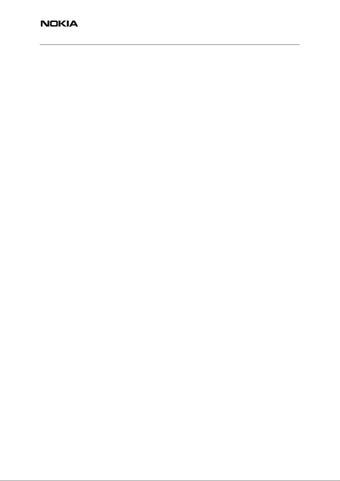
■ Block diagram
Figure 1:Baseband block diagram
UEMEK supplies both baseband and RF with power via built in voltage regulators, which are
connected to the battery . The RF pa rts use mainly 2.78 V and the baseband p arts 1.8V I/O voltage. The UPP core is supplied with programmable core voltage of 1.0V, 1.3V or 1.5V . UEMEK
includes 7 linear LDO (Low Drop-Out) regulators for baseband and 7 regulators for RF. It also
includes 4 current sources for biasing purposes and internal usage. The UEMEK is furthermore
supplying the SIM interface with a programmable voltage of 1.8V or 3V.
Note: 5V SIM cards are no longer supported by DCT-4 generation Baseband.
UPP operates from a 26 MHz clock coming from the RF ASIC Helgo. The clock signal is divided
by two down to the nominal system clock frequency of 13 MHz. The DSP and MCU contain
PLLs, which can multiply the system clock to a higher frequency.
A real time clock function is integrated into the UEMEK, which utilizes the same 32kHz clock
supply as the sleep clock.
The communication between UEMEK and UPP is implemented using two bi-directional serial
busses, CBUS and DBUS. The CBUS is controlled by the MCU and operates at a speed of 1
MHz. The DBUS is controlled by the MCU and operates at a speed of 13 MHz. Both processors
are located in the UPP.
Issue 1 04/2005 COMPANY CONFIDENTIAL 9
Copyright © 2005 Nokia. All Rights Reserved.
Page 10

RM-94
Nokia Customer Care 7 - System Module
The UEMEK ASIC handles the analog interface between the Baseband and the RF section.
UEMEK provides A/D and D/A conversion of the in-phase and quadrature receive and transmit
signal paths and also A/D and D/A conversions of received and transmitted audio signals to
and from the user interface. The UEMEK supplies the analog TXC and AFC sign als to the RF
section according to UPP signal control. There are also separate signals for PDM coded audio.
Digital speech processing is handled by the DSP inside UPP ASIC.
UEMEK is a dual voltage circuit, the digital parts are running from the baseband supply 1.8V
and the analog parts are running from the analog supply 2.78V or backup battery. Also VBAT
is directly used (Vibra, LED-driver, Camera Regulator).
The Baseband supports both internal and external microphone inputs and speaker outputs.
Keypad tones, DTMF , and other audio tones are generated and encoded by the UPP and transmitted to the UEMEK for decoding. An external vibra alert control signals are generated by the
UEMEK with separate PWM outputs.
EMC shielding is implemented using a soldered shielding, RF cans and PWB grounding.
10 COMPANY CONFIDENTIAL Issue 1 04/2005
Copyright © 2005 Nokia. All Rights Reserved.
Page 11
RM-94
7 - System Module Nokia Customer Care
■ Frequencies in baseband
Table 1: Frequencies in baseband
Frequency Context UPP UEMEK Flash SIM Comment
32 kHz SleepClk X
1 MHz CBUS X X
Up to 1 MHz RFConvClk X X Estimation
6,5 MHz Display IF X
3,25 MHz SIMIF X X Min
13 MHz DBUS, RFBUClik X X
26 MHz RF Clk X
52 MHz Memory Clock X X
■ PWB
Characteristics of the PWB
•Single PWB
• 8 layer board
• Double side assembled
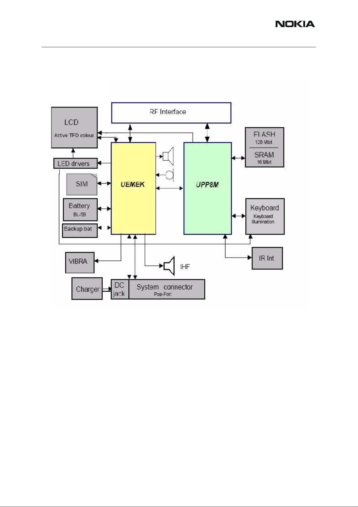
Key components
Figure 2:Key components
Issue 1 04/2005 COMPANY CONFIDENTIAL 11
Copyright © 2005 Nokia. All Rights Reserved.
Page 12
RM-94
Nokia Customer Care 7 - System Module
Table 2: Key components
Position Component Name
D1470 HW Accelerator
D2800 UPP8M V4.2E
D2200 UEMEKv2.0
D3000 Combo Memory (128M NOR + 16M
UTRAM)
12 COMPANY CONFIDENTIAL Issue 1 04/2005
Copyright © 2005 Nokia. All Rights Reserved.
Page 13

RM-94
7 - System Module Nokia Customer Care
Technical Specifications
■ Baseband core
UPP
Main characteristics of the used UPP are:
• DSP, LEAD3 16 bit DSP core 32 bit IF max. 200 MHz
• MCU based on ARM7 RISC MCU core max 50 MHz
• Internal 8 Mbit SRAM (PDRAM)
• General purpose UARTS
• SIM card interface
• Accessory interface (ACI)
• Interface control for Keypad, LCD, Audio and UEM control
• Handling of BB-RF Interface
UEMEK
Main characteristics of the used UEMEK are:
• ACI support
• Audio codec
• 11 Channel A/D converter
• Auxiliary A/D converter
• 32 KHz crystal oscillator
• SIM interface and drivers
• Security logic
• Storage of IMEI code
• Buzzer and vibra motor drivers
•PWM
• 2 LED drivers, keyboard and display backlight drivers
• Voltage reference for analogue blocks
• Charging function
• Baseband regulators
• RF regulators
• RF interface converters
Issue 1 04/2005 COMPANY CONFIDENTIAL 13
Copyright © 2005 Nokia. All Rights Reserved.
Page 14

RM-94
Nokia Customer Care 7 - System Module
External SRAM and Flash
The Combo-Memory is a multi chip package memory which combines 128 Mbit (8Mx1 6) muxed
burst multibank flash and 16 Mbit muxed CMOS PSRAM (Pseudo SRAM: DRAM with SRAM
interface).
The combo is supplied by single 1,8 V for read, write and erase operations. For accelerated
flash programming, Vpp = 9.0 V has to be applied to VPP input of the combo device.
The combo memory is housed in a 44-ball FBGA.
■ Energy management
The energy management of RM-94 is based on BB 4.0 architecture. A so-called semi fixed battery (BL-5B) supplies power primarily to UEMEK ASIC and the RF PA. The UEMEK includes
several regulators to supply RF and Baseband. It provides energy management including power up/down procedure.
Modes of operation
The baseband engine has six different functional modes: Since the UEMEK controls the regulated power distribution; each of these states affects the general functionality of the phone.
1. No supply
2. Backup
3. Acting Dead
4. Active
5. Sleep
6. Charging
No Supply
In NO_SUPPLY mode, the phone has no supply volt age. This mode is due to the disconnection
of the main battery and backup battery or low battery voltage level in both of the batteries.
The phone is exiting from NO_SUPPLY mode when sufficient battery voltage level is detected.
The battery voltage can rise either by connecting a new battery with VBA T > V
necting charger and charging the battery above V
MSTR+
.
MSTR+
or by con-
Backup
In BACKUP mode the backup battery has suf ficient charge but the main battery can be discon-
nected or empty (VBAT < V
The VTRC regulator is disabled in BACKUP mode. VRTC output is supplied witho ut regulation
from the backup battery (VBACK). All the other regulators are disabled.
and VBACK > VBU
MSTR
COFF
).
Acting Dead
If the phone is off when the charger is connected, the phone is powered on but enters a state
called ”Acting Dead”. To the user, the phone acts as if it was switched off. A battery-charging
alert is given and/or a battery charging indication on the display is shown to acknowledge the
user that the battery is being charged.
14 COMPANY CONFIDENTIAL Issue 1 04/2005
Copyright © 2005 Nokia. All Rights Reserved.
Page 15

RM-94
7 - System Module Nokia Customer Care
Active
In Active mode, the phone is in normal operation, scanning for channels, listing to a base station, transmitting and processing information.
Sleep Mode
Sleep mode is entered when both MCU and DSP are in stand–by mode. Both processors control the sleep mode.
The sleep mode is exited either by the expiration of a sleep clock counter in the UEMEK or by
some external interrupt, generated by a charger connection, key press, headset connection
etc.
In the sleep mode, VCTCXO is shut down and 32 kHz sleep clock oscillator is used as reference clock for the Baseband.
Charging
In RM-94, the battery type/size is indicated by a BSI-resistor. The resistor value corresponds
to a specific battery capacity. Also BTEMP, NTC resistor, is located on an engine board.
The battery voltage, temperature, size and current are measur ed by the UEMEK controlle d by
the charging software running in the UPP.
The charging control circuitry (CHACON) inside the UEMEK controls the charging current delivered from the charger to the battery . The battery volt age rise is limited by turning the UEMEK
switch off when the battery voltage has reached 4.2 V. Charging current is monitored by measuring the voltage drop across a 220 mΩ resistor.
■ Power distribution
Under normal conditions, the battery powers the baseband module. Individual regulators located within the UEMEK regulate the battery voltage VBAT. These regulators supply the different
parts of the phone. 7 regulators are dedicated to the RF module and 7 to the baseband module.
The VSIM regulator is able to deliver both 1,8V and 3,0 V DC and thus supporting two different
SIM technologies.
The system connector provides a voltage to supply accessories.
The white LEDs need a higher voltage supply than the battery can supply and are fed by a sep-
arate external voltage regulator.
VBAT is directly distributed to the RF power amplifier, FCI and external baseband regulators.
Issue 1 04/2005 COMPANY CONFIDENTIAL 15
Copyright © 2005 Nokia. All Rights Reserved.
Page 16

RM-94
Nokia Customer Care 7 - System Module
Figure 3:Power Distribution Diagram
■ DC characteristics
Supply voltage ranges
Signal Min Nom Max Note
VBAT 3.1V 3.7V 4.2V 3.2V SW cut off
Table 3: Battery voltage ranges
2.95V HW power off
16 COMPANY CONFIDENTIAL Issue 1 04/2005
Copyright © 2005 Nokia. All Rights Reserved.
Page 17

RM-94
7 - System Module Nokia Customer Care
Baseband regulators
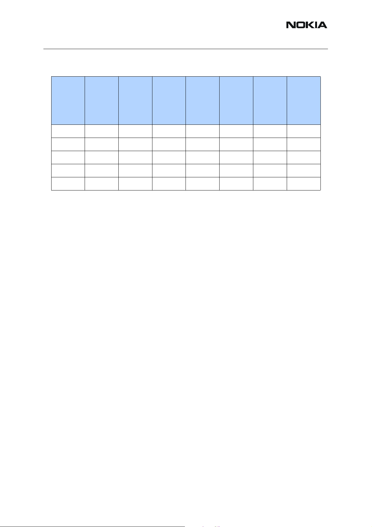
Table 4: Regulator specification
Regulator
Load current
(mA)
Limit (V) Min/Max (Typ)
VCORE 200 1.476 / 1.65 (1.57)
VIO 150 1.72 / 1.88 (1.8)
VSIM1 25 1.745 / 1.855 (1.8)
VANA 80 2.70 / 2.86 (2.78)
VFLASH1 70 2.70 / 2.86 (2.78)
VAUX2 70 2.70 / 2.86 (2.78)
VAUX3 10 2.70 / 2.86 (2.78)
VR2 100 2.70 / 2.86 (2.78)
VR3 20 2.70 / 2.86 (2.78)
VR4 50 2.70 / 2.86 (2.78)
VR5 50 2.70 / 2.86 (2.78)
VR6 50 2.70 / 2.86 (2.78)
VR7 45 2.70 / 2.86 (2.78)
VR1A 5* 4.6 / 4.9 (4.75)
VR1B 5* 4.6 / 4.9 (4.75)
* When both enabled. Load current is 10 mA if other is disabled.
Note: This list shows the band regulators only. Please see other descriptions in th e Glossary of
Terms and in the dedicated sections.
Issue 1 04/2005 COMPANY CONFIDENTIAL 17
Copyright © 2005 Nokia. All Rights Reserved.
Page 18

RM-94
Nokia Customer Care 7 - System Module
Function Groups
■ Battery
A battery of the type BL-5B is used. It is a Li Ion based standard cell. The battery capacity is
760mAh.
The battery has a three-pin connector. In order to get temperature information of the battery,
the NTC mounted on the PWB within the BB area is used.
Ni based batteries are not supported.
The BSI resistor has a nominal value of 75 kOhm.
Figure 4:Battery BL-5B
■ Audio
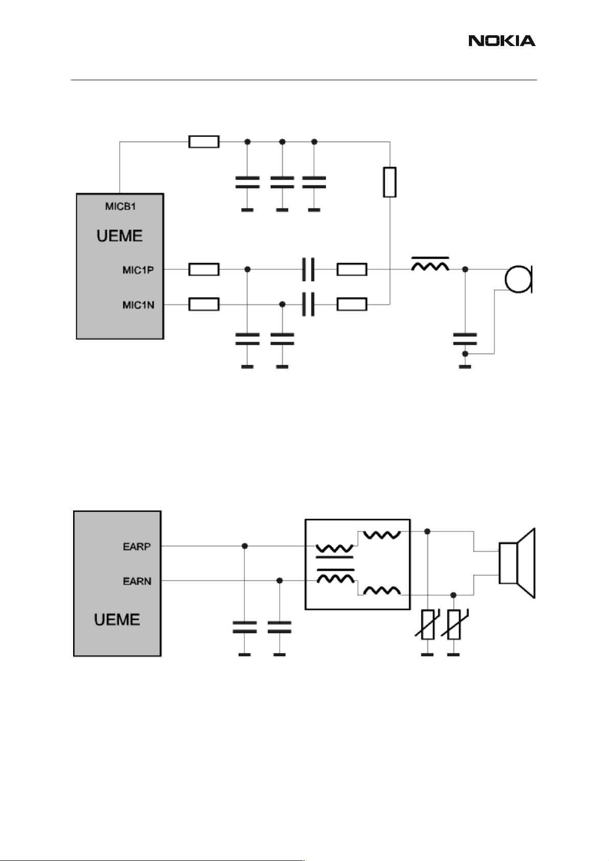
Internal microphone
The internal microphone capsule is mounted to in the PopPortTM system connector . The microphone is omni directional and it’s connected to the UEMEK microphone input MIC1P/N. The
microphone input is symmetric and the UEMEK (MICB1) provides bias voltage. The microphone input on the UEMEK is ESD protected. Spring contacts are used to connect the microphone to the PWB.
18 COMPANY CONFIDENTIAL Issue 1 04/2005
Copyright © 2005 Nokia. All Rights Reserved.
Page 19
RM-94
7 - System Module Nokia Customer Care
Figure 5:Internal microphone connection
Internal speaker
The internal earpiece is a dynamic earpiece with an impedance of 32 ohms. The earpiece is
low impedance one since the sound pressure is to be generated using current and not volta ge
as the supply voltage is restricted to 2.7V. The earpiece is driven directly by the UEMEK and
the earpiece driver (EARP & EARN outputs) is a fully dif ferential bridge amplifier with 6 dB gain.
Figure 6:Speaker connection
Issue 1 04/2005 COMPANY CONFIDENTIAL 19
Copyright © 2005 Nokia. All Rights Reserved.
Page 20

RM-94
Nokia Customer Care 7 - System Module
IHF speaker
UEMEK has an integrated Audio power amplifier to generate output for the IHF speaker . Block
diagram of IHF.
For RM-94, the Integrated Hands Free Speaker is used to generate hands free speech, and
also polyphonic ringing tones. The speaker capsule is mounted into the A Cover, and spring
contacts are used to connect the IHF Speaker contacts to the PWB.
The IHF is furthermore used to generate alerting and warning tones.
External audio
RM-94 is designed to support a fully differential external audio accesso ry co nnection. A headset can be directly connected to the PopPort
ed by RM-94. A stereo headset can be connected to RM-94, since left and right paths are
connected in parallel at the PopPort
TM
TM
system connector . Stereo audio is not support-
connector.
External microphone connection
The external microphone input is fully differential and lines are connected to the UEMEK microphone input MIC2P/N. The UEMEK (MICB2) provides bias voltage. Microphone input lines
are ESD protected.
Headset connections
Headset implementation uses separate microphone and earpiece signals. The accessory is detected by the ACI signal when the plug is inserted.
Test possibilities
Phoenix audio test
For troubleshooting see Audio faults in Baseband Troubleshooting Instructions.
■ Vibra
A vibra alerting device is used to generate a vibration signal for an incoming call. The vibra is
located in the bottom end of the phone and connection is done with SMD. The vibra is control-
20 COMPANY CONFIDENTIAL Issue 1 04/2005
Copyright © 2005 Nokia. All Rights Reserved.
Page 21

RM-94
7 - System Module Nokia Customer Care
led by a PWM signal from the UEMEK. The Frequency can be set to 64, 129, 258 or 520 Hz
and duty cycle can vary between 3% and 97%.
Test possibility
Phoenix Vibra Test
■ LCD module
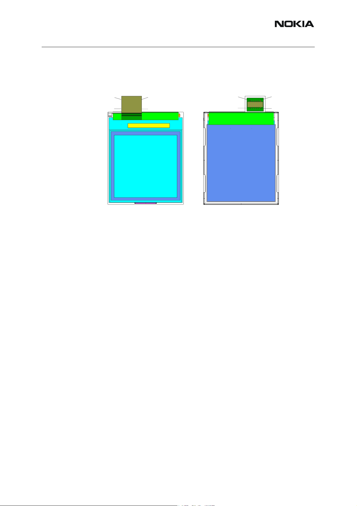
RM-94 has a 130 x 130 16 bpp (bits per pixel) active matrix color display . The number of colours
is 64k, i.e. 16 bits. The LCD Interface is using serial 9-bit dat a transfer . The L CD display is connected to transceiver PWB by board-to-board connector.
Characteristics
Table 5: LCD Characteristics
Active display area format 130 columns x 130 rows
UserInterface display area format 128 columns x 128 rows
Module size (width x height x thickness) 33,9 mm x 41.3 mm x 3.225 mm
Interface 9-bit serial
Illumination mode Transflective, Normally white
Number of LEDs 3 white LED
Numbers of
colors supported
by interface
Pixel height to width ratio 1:1
Viewing direction 6 o´clock
Refresh rate 55 Hz +- 10%
Full mode 65K 16-bit 5xR, 6xG, 5xB
Issue 1 04/2005 COMPANY CONFIDENTIAL 21
Copyright © 2005 Nokia. All Rights Reserved.
Page 22
RM-94
Nokia Customer Care 7 - System Module
LCD connector
The TE signal is not used.
Table 6: LCD connector
Pin
No:
1 Power supply OUT VLED- LED power supply cur-
2 Power supply
3 Ground - GND
4 Bidirectional
5 Chip select IN CSX Input voltage high 0.7 x
Description Type Symbol Parameter Min Typical Max Unit
rent
IN VDDI Operating voltage 1.65 1.8 1.95 V
voltage
I/O SDA Input voltage high 0.7 x
serial data
Input voltage low 0 0.3 x
Output voltage high @ -
1.0 mA
Output voltage low @ -
1.0 mA
Input voltage low 0 0.3 x
VDDI
0.8 x
VDDI
0 0.2 x
VDDI
15 mA
VDDI V
VDDI
VDDI
VDDI
VDDI V
VDDI
6 Ground - GND
7 TE output to syn-
chronise MCU to
frame writing
8 Reset IN RESX Input voltage high 0.7 x
9 Serial clock IN SCL Input voltage high 0.7 x
10 Ground - GND
11 Power supply
voltage
12 Power supply IN VLED+ LED power supply cur-
OUT TE Output voltage high @ -
1.0 mA
Output voltage low @ -
1.0 mA
Input voltage low 0 0.3 x
Input voltage low 0 0.3 x
IN VDD Operating voltage 2.6 2.75 2.9 V
rent
0.8 x
VDDI
0 0.2 x
VDDI
VDDI
VDDI V
VDDI
VDDI V
VDDI
VDDI V
VDDI
15 mA
22 COMPANY CONFIDENTIAL Issue 1 04/2005
Copyright © 2005 Nokia. All Rights Reserved.
Page 23
RM-94
7 - System Module Nokia Customer Care
Figure 7:LCD display
Connector type (Plug) Hirose DF23C-12DP-0.5V
6
1
127
Top view
1
12
Back view
Test possibility
Phoenix Display Test
For troubleshooting see Display faults in Baseband Troubleshooting Instructions.
6
7
Issue 1 04/2005 COMPANY CONFIDENTIAL 23
Copyright © 2005 Nokia. All Rights Reserved.
Page 24
RM-94
Nokia Customer Care 7 - System Module
■ Keypad
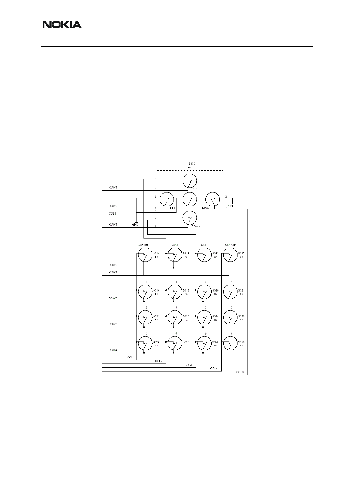
The RM-94 keys are connected to the UPP via the KEYB(10:0) bus. The keypad consists of a
5x4 matrix of 5 rows, ROW0 – ROW4, and 4 columns, COL1 – COL4.
Additionally, there are 3 lines that are directly connected to the UPP IO and can be detected
independently. COL5 is connected to GENIO0.
Test possibility
Phoenix Keyboard Test
For troubleshooting, see Keypad faults in Baseband Troubleshooting Instructions.
Figure 8:RM-94 keypad
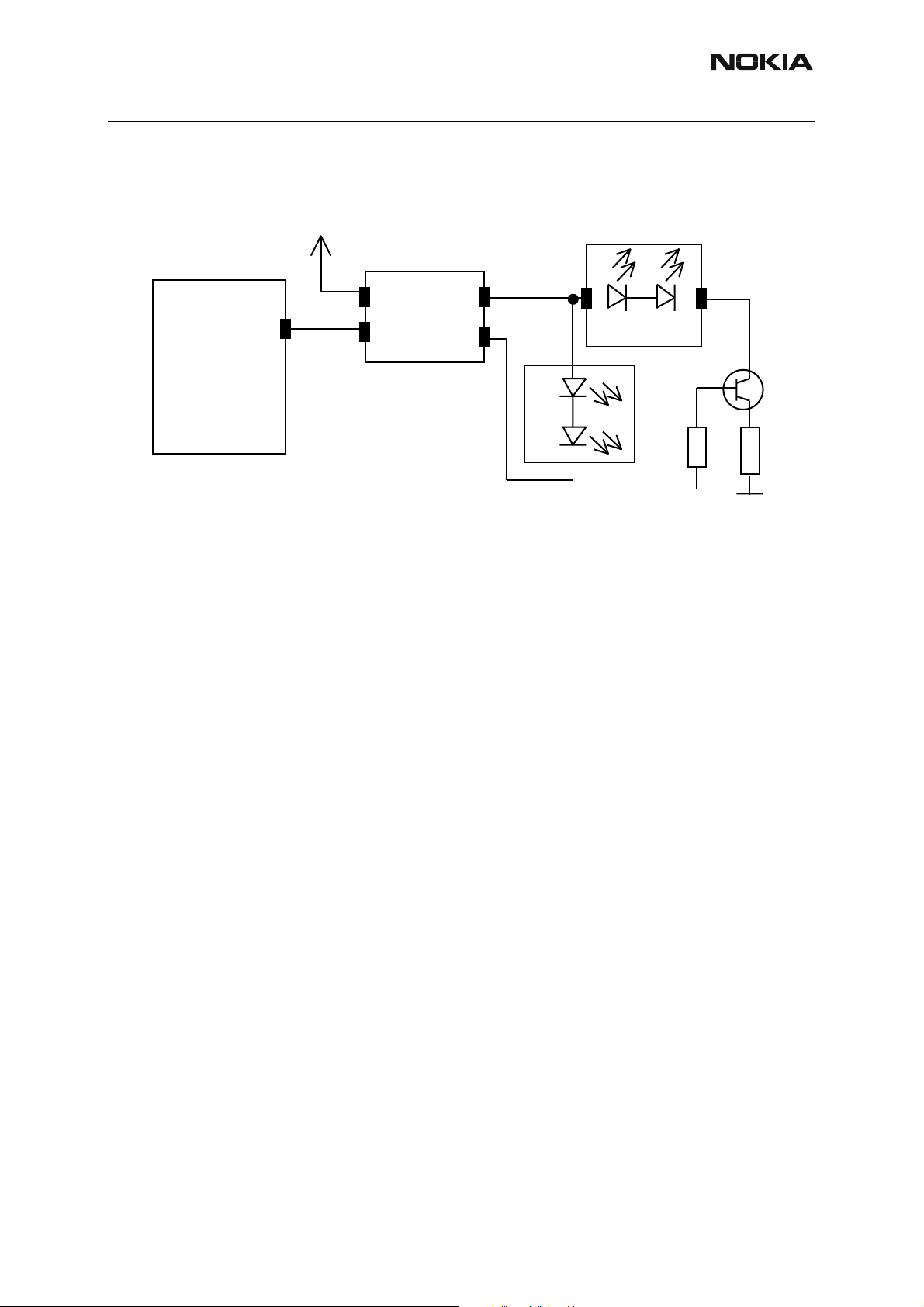
■ Illumination
In RM-94, white LED’s are used for the LCD backlight and keypad lighting. Three LED’s are
used for the LCD lighting and two LED’s for the keyboard. A step up DC-DC conve rter is used
as a LED driver that is configured as a constant current source.
24 COMPANY CONFIDENTIAL Issue 1 04/2005
Copyright © 2005 Nokia. All Rights Reserved.
Page 25
RM-94
V
V
V
V
7 - System Module Nokia Customer Care
Figure 9:Illumination
Keybord light
UEME
DLIGHT
BAT
DC/DC-Converter
in
EN
LED+
LED-
LCD Backlight
GEN I/O 19
Test possibility
Phoenix LED test
For troubleshooting see Display faults in Baseband Troubleshooting Instructions.
■ SIM
The whole SIM interface locates in UPP and UEMEK.
The interface part in the UEMEK contains po wer up/down, port gating, card detect, dat a receiv-
ing, ATR-counter, registers and level shifting buffers logic. The SIM interface is the electrical
interface between the Subscriber Identity Module Card (SIM Card) and mobile phone (via
UEMEK device).
Both 3V and 1.8V SIM cards are supported. A register in the UEMEK selects SIM supply voltage. It is only allowed to change the SIM supply voltage when the SIM IF is powered down.
Issue 1 04/2005 COMPANY CONFIDENTIAL 25
Copyright © 2005 Nokia. All Rights Reserved.
Page 26

RM-94
)
Nokia Customer Care 7 - System Module
Figure 10:UPP/UEMEK SIM Interface Connections
SIM
UPP
SIMIO
SIMClk
SIMRst
UIF Block
UEMEInt
CBusDa
CBusEnX
CBusClk
SIM
ASIP
From battery
type contact
SIMIO
SIMClk
SIMRst
VSIM
BSI
UEME
SIMIO
SIMClk
SIMRst
SIMIF
register
UEME
digital
logic
Test possibility
Phoenix SIM Test
For troubleshooting, see SIM Card faults in Baseband Troubleshooting Instructions.
■ IR module
RM-94 has an IR module. The IR link supports speeds from 9600 bit/s to 1.152 Mbit/s u p to a
distance of 80 cm. Transmission over the IR if is half-duplex.
The IR transceiver can be set into SIR or MIR modes. In SIR mode the transceiver is capable
of transmission speed up to 115.2 kbit/s. In MIR mode faster transmission speeds are used.
The maximum speed is 1.152 Mbit/s. The IR transceiver can be set into shu tdown mode by setting SD pin to logic ‘1’ for current saving reasons.
Figure 11: IR interface
26 COMPANY CONFIDENTIAL Issue 1 04/2005
Copyright © 2005 Nokia. All Rights Reserved.
Page 27

RM-94
7 - System Module Nokia Customer Care
Interfaces
■ BB-RF interface
The interface between the Baseband and RF can be divided into three categories:
• The digital interface from UPP to the RF ASIC (Helgo). The serial digital interface
is used to control the operation of different blocks in the RF ASICs
• The analogue interface between Baseband and RF. The analogue interface consists of Tx and Rx converter signals. The power amplifier control signals TXC and
AFC also come from the UEMEK.
• Reference clock interface between Helgo and UPP which supplies the 26 MHz
system clock for UPP.
■ System connector interface
System connector
The system connector is a galvanic interface between phone and accessory.
Four new functions are introduced with the PopPort
TM
IF; Accessory Control Interface (ACI),
Power Out; Stereo audio output and Universal Serial Bus (USB). The USB functionality is not
supported by RM-94. The RM-94 product supports “double mono” on the earpiece lines. The
MBUS function, (included in previous accessory interfaces) is not supported by this interface.
The connector is not backward compatible with DCT1, DCT2 and DCT3 accessory interfaces.
Figure 12:PopPort™ bottom connector (charger plug socket & PopPort™ system con-
nector)
1 2 14
Charge
Charge GND
Charge
Shielding GND
ACI
Charge GND
Vout
USB
Fbus SB D+ _RX / U
Vbus
Data GND
Fbus_Tx / USB D-
XMICP
XMICN
XEARN
XEARRN
XEARP
XEARRP
Shielding GND
Issue 1 04/2005 COMPANY CONFIDENTIAL 27
Copyright © 2005 Nokia. All Rights Reserved.
Page 28

RM-94
Nokia Customer Care 7 - System Module
Table 7: System connector interface description
Pin # Signal Notes
1 VCHAR
2 GND Charge ground
3 ACI Insertion & removal detection /
Serial data bi-directional 1 kbit/s
4 Vout Power supply for external accessories
5 Not used in RM-94
6 FBUS_RX Serial data from accessory to phone /
11 5 kbit/s
7 FBUS_TX Serial data from phone to accessory /
11 5 kbit/s
8 GND Data ground
9 XMIC N Negative audio in signal
10 XMIC P Positive audio in signal
11 HSEAR N Negative audio out signal.
12 HSEAR P Positive audio out signal.
13 HSEAR RN Negative audio out signal.
14 HSEAR RP Positive audio out signal.
ACI
ACI (Accessory Control Interface) is a point-to-point, Master-Slave, bi-directional serial bus.
ACI has two main features:
• The identification of accessory type is provided
• The insertion and removal detection of an accessory device
• Acting as a data bus, intended mainly for control purposes.
FBUS
FBUS is an asynchronous data bus having separate TX and RX signals. Default bit rate of the
bus is 115.2 Kbit/s. FBUS is mainly used for controlling the phone in the interface to PC via
DKU-5.
VOUT
The VOUT pin delivers the power supply for PopPortTM accessories, which are using the ACI
or FBUS. The voltage level is 2.78V / 70mA.
28 COMPANY CONFIDENTIAL Issue 1 04/2005
Copyright © 2005 Nokia. All Rights Reserved.
Page 29

RM-94
7 - System Module Nokia Customer Care
DC plug
NMP standard 2- or 3-wire chargers are comp atible with the charger IF . The IF doe s not support
3-wire charging control. Nevertheless, it is potential possible to use a 3-wire charger without
PWM charging support. RM-94 uses a 3mm DC plug besides the PopPort
TM
IF.
Issue 1 04/2005 COMPANY CONFIDENTIAL 29
Copyright © 2005 Nokia. All Rights Reserved.
Page 30

RM-94
Nokia Customer Care 7 - System Module
RF Module Description
The RF module performs the necessary high frequency operations of the triple-band engine.
Both the transmitter and receiver have been implemented by using a direct conversion architecture, which means that the modulator and demodulator operate on the channel frequency.
No intermediate frequencies are used for up- or down-conversion.
The core of the RF is an application-specific integrated circuit (RF ASIC), Helgo85. The other
RF key components are:
• An EDGE capable power amplifier module, which includes two amplifier chains,
one for the low band (GSM900) and the other for both high bands (GSM1800 and
GSM1900).
• An antenna switch module, which contains filters and switches to combine the two
TX-PA outputs and three Rx chain inputs to the antenna port.
• 26 MHz reference oscillator (VCTCXO).
• 3296-3980 MHz VCO.
• Three SAW filters for Rx band filtering.
• One SAW filter for the low band (GSM900) Tx path.
The control information for the RF is coming from the baseband section of the engine through
a serial bus, referred later on as RFBus. This serial bus is used to pass the infor mation on the
frequency band, mode of operation, and synthesizer channel for the RF. In addition, exact timing information and receiver gain settings are transferred through the RFBus.
Physically , the bus is located between the baseband ASIC called UPP and the RF ASIC. Using
the information obtained from UPP, the RF ASIC controls itself to the required mode of operation and further sends control signals to the antenna switch and the power amplifier modules.
In addition to the RFBus, there are still other interface signals for the power control loop and
VCTCXO control and for the modulated waveforms (IQ signals).
The RF circuitry is located in two shielding chambers on one side of the 8 layer PWB containing
the following key components: The Small Signal Chamber contains RF ASIC, reference oscillator (VCTCXO), VCO, and Rx/Tx SAW-filters (GSM900/GSM1800). The Large Signal Chamber contains the RF Power Amplifier, the Antenna Switch Module, and the Rx SAW-filter and
LNA (GSM1900).
30 COMPANY CONFIDENTIAL Issue 1 04/2005
Copyright © 2005 Nokia. All Rights Reserved.
Page 31

RM-94
7 - System Module Nokia Customer Care
■ General specifications of the transceiver
Parameter Unit
Cellular System GSM900, GSM1800, GSM1900
Modulation schemes GMSK, 8-PSK
RX Frequency Band GSM900: 925 … 960 MHz
GSM1800: 1805 ... 1880 MHz
GSM1900: 1930 … 1990 MHz
TX Frequency Band GSM900: 880 … 915 MHz
GSM1800: 1710 ... 1785 MHz
GSM1900: 1850 … 1910 MHz
Output Power GMSK GSM900: +5 … +33 dBm (3.2 mW … 2 W)
GSM1800: +0 … +30 dBm (1.0 mW … 1 W)
GSM1900: +0 … +30 dBm (1.0 mW … 1 W)
Output Power 8-PSK GSM900: +5 … 27 dBm (3.2 mW … 0.5 W)
GSM1800: +0 … 26 dBm (1.0 mW … 0.4 W)
GSM1900: +0 … 26 dBm (1.0 mW … 0.4 W)
Duplex Spacing GSM 900: 45 MHz
GSM 1800: 95 MHz
GSM 1900: 80 MHz
Number of RF Channels GSM 900: 174
GSM 1800: 374
GSM1900: 299
Channel Spacing 200 kHz (each band)
Number of TX Power Levels
GMSK
Number of TX Power Levels
8-PSK
Sensitivity, static channel
(+25°C)
GSM 900: 15
GSM 1800: 16
GSM 1900: 16
GSM 900: 12
GSM 1800: 14
GSM 1900: 14
GSM 900: -102 dBm
GSM 1800: -102 dBm
GSM 1900: -102 dBm
Frequency Error, static channel < 0,1 ppm
RMS Phase Error < 5.0°
Peak Phase Error < 20.0°
Issue 1 04/2005 COMPANY CONFIDENTIAL 31
Copyright © 2005 Nokia. All Rights Reserved.
Page 32

RM-94
Nokia Customer Care 7 - System Module
■ Frequency concept
The RF frequency plan is shown below . The VCO operates at the channel frequency multiplied
by two or four depending on the frequency band of operation. This means that the modulated
signals from baseband are directly converted up to the transmission frequency and the received RF signals directly down to the baseband frequency.
Figure 13:RF frequency plan
Helgo
SM900: 92 5- 9 60 MH z
SM1800: 1805-1880 MHz
SM1900: 1930-1990 MHz
I-signal
Q-signal
RX
f/2
f/2
f
32963980
MHz
f
PLL
AFC
26 MHz
VCTCXO
Buffer
VCTCXO
26 MHz
I-signal
Q-signal
TX
f/4
f
f
f/4
SM1800: 1710-1785 MHz
SM1900: 1850-1910 MHz
SM850: 82 4- 8 49 MH z
SM900: 88 0- 9 15 MH z
■ RF power supply configuration
All power supplies for the RF unit are generated in the UEM ASIC, which contains among other
functions six pieces of 2.78 V linear regulators (VR2 ... VR7), a 4.8 V switching regulator (VR1)
and two 1.35V voltage references (VrefRF01 and VrefRF02).
The regulators are connected to the RF ASIC, except for VR7, which supplies the VCO. The
4.8V supply is required for the charge pump of the PLL to generate the tuning voltage for the
VCO.
The reference voltages are used as bias reference for the RF ASIC for the RX ADC (analogto-digital converter) reference.
All RF supplies can be checked either in Small Signal Chamber or in BB Chamber.
The used power supply configuration is shown in the block diagram below. Values of volt ages
are given as nominal outputs of UEM. Currents are typical values.
32 COMPANY CONFIDENTIAL Issue 1 04/2005
Copyright © 2005 Nokia. All Rights Reserved.
Page 33
RM-94
7 - System Module Nokia Customer Care
Figure 14:RF power distribution diagram
UEM
VR1
VR2
VR3
VR4
VR5
VR6
4.75 V [ 4.6V ... 4.9V ]
2.78 V [ 2.70V ... 2.86V ]
2.78 V [ 2.70V ... 2.86V ]
2.78 V [ 2.70V ... 2.86V ]
2.78 V [ 2.70V ... 2.86V ]
2.78 V [ 2.70V ... 2.86V ]
charge pump (VCP)
Tx modulator (Vcc_ModOut)
TX buffer & EDGE ALCs (VRF_TX)
VCTCXO (+VCC)
digital interface (VDIG)
Rx Front End (VRF_RX)
Bias & Rx CH filters (VF_RX)
RF controls (VPAB_VLNA)
PLL prescaler (VPRE)
phasing dividers of Rx (VLO)
BB buffer (VDIG)
VR7
V
refRF01
V
refRF02
VBAT
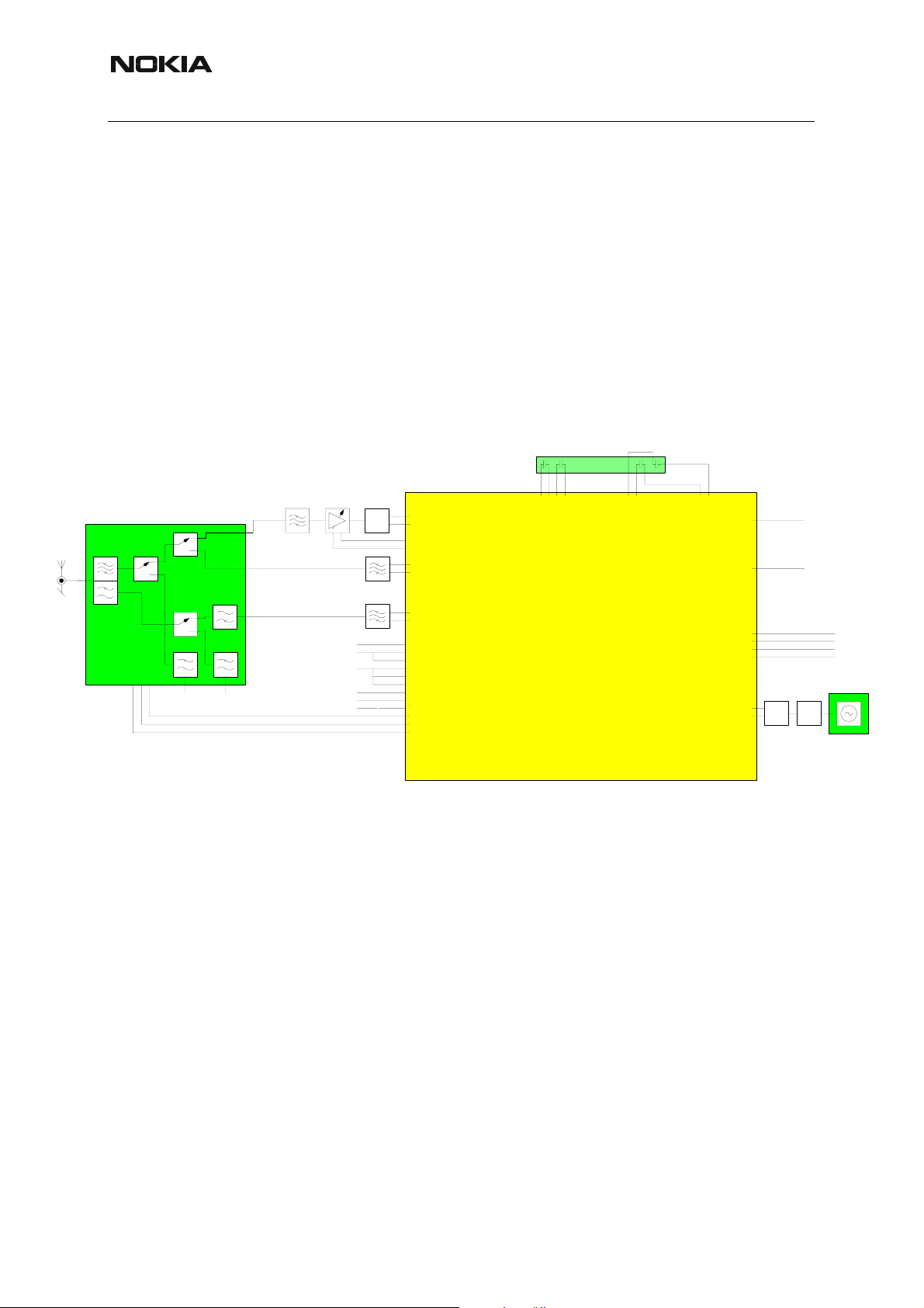
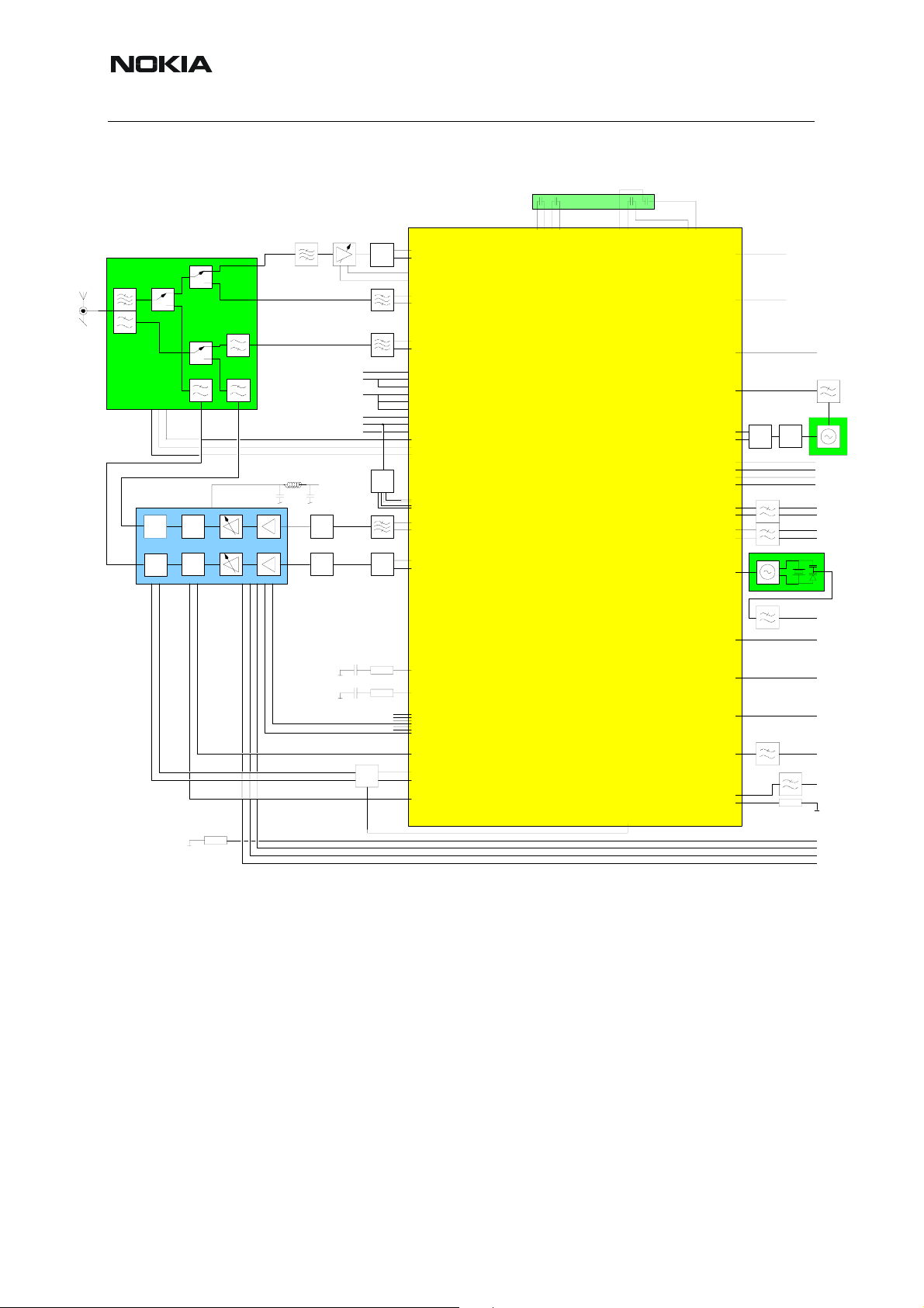
■ RF block diagram
RF block diagram consists of:
• Antenna switch module
• Power amplifier module
• RF ASIC
• VCTCXO module
• VCO module
2.78 V [ 2.70V ... 2.86V ]
16 mA [max. 20 mA]
1.35 V [ 1.32V ... 1.38V ]
100 uA
1.35 V [ 1.32V ... 1.38V ]
100 uA
3.7 V [ 2.95V ... 4.7V ]
VCO (VCC_VCO)
bias reference (VB_EXT)
bias reference
Triple band PA
(RXIINN, RXQINN)
Issue 1 04/2005 COMPANY CONFIDENTIAL 33
Copyright © 2005 Nokia. All Rights Reserved.
Page 34

RM-94
Nokia Customer Care 7 - System Module
Figure 15: RF block diagram
RF Fron t-en d Module
HB BP
LC
LB LP
LC
Edge capabl e PA Module
1900 Rx
SAW
ESD
FILTER
900 Tx
1900 Tx
LC
LC
CTRL inputs
VBAT
800/900
internal
Det.
matchi ng
1800/1900
internal
Det.
matchi ng
Vtxb 850/900Iref 850/900Iref 1 800/1 900Vdetect 850/900Vdetec t 1800 /1900 Vpctr l 850/90 0Vpctrl 1800/1 900 Vmode
3dB att
3dB att
Vtxb 180 0/1900
Balun
LNAB_P
LNA_P
1800 Rx
SAW
900 Rx
SAW
EGSM
Pull-up
Network
900 Tx
VBB
VLO
VPRE
VRF_RX
VF_RX
VPAB_VLNA
VDIG
VRF_TX
VCP
VRF_TX,VBB,VLO,VTX
Analog AGC
SAW
EGSM
Analog AGC
Balun
VR6
VR5
VR4
VR3
VR2
VR1
VRF_RXVLNA
VF_RX
INTEGRATED
LOW-PASS FILTERS
AND AGC FUNCTION
BUILT-IN DC COMP.
Digita l A GC
Digita l A GC
Digita l A GC
Digita l A GC
VLO
Divide
by 2/4
1k2
s7
s3
VBB
2.7V
10mA
GPIO
VBB
VDIG
VPRE,VDIG,VCP
Bi-directional
Serial
Interfa ce
VDIG
VDIG
temp
sensor
PLL
Divide
by two
Balun
VR3
VCTCXO Module
RXIP
RXQP
RFTEMP
VR7
2 dB
Att
VCO Module
RESET
SLE
SCLK
SDATA
TXIP
TXIM
TXQP
TXQM
AFC D/A
REFCLK
TXA
8-PSK Feed-back
GMSK Feed-back
VBB, GND_BB
s6
PCTRL enable
s1
s5
s2
VDIG
VB_ext
bias
RB_ext
gen
R_ref
PA Detect
detector
feedback
network
Helgo
2.7V
10/40mA
GPIO
VPAB,VBB
Helgo
A detailed functional description is given in the following sections.
■ Antenna switch (TX/RX switch)
The antenna switch operates as a diplexer for the RX and TX signals. The antenna switch is
controlled by the RF ASIC using the control signals VANT1, VANT2 and VANT3.
The table below shows the possible different switching states.
TXP
TXC
V_ref_RF01
PA ID
Iref 850/900
Iref 18 00/190 0
MODE
34 COMPANY CONFIDENTIAL Issue 1 04/2005
Copyright © 2005 Nokia. All Rights Reserved.
Page 35
RM-94
7 - System Module Nokia Customer Care
VANT_2
VC1
[Volt]
VANT_3
VC2
[Volt]
VANT_1
VC3
[Volt]
Rx1
GSM
900
Rx
Rx2
GSM
1800
Rx
Rx3
GSM
1900
Rx
Tx1
GSM
900
Tx
Tx2
GSM
1800/1900
Tx
000X
000 X
02.62.6 X
02.60 X
2.6 2.6 0 X
To switch the TX-GSM 1800/1900 path both signals VANT2 and VANT3 have to be a ctivated .
Receiver
Each receiver path is a direct conversion linear receiver. From the antenna, the received RF
signal is fed to the antenna switch module where a diplexer first divides the signal to two separate paths for the low band and the two high bands. Then the paths are passing the Rx/Tx
switches and the high band signal passes an additional GSM1800/1900 switch. As output of
the module three separate Rx connections are available.
These signals are fed to the SAW band filters, which let only the frequencies of the wanted
band pass on to the low noise amplifiers. The GSM1900 LNA is an external component, the
other two LNAs are integrated in the RF ASIC.
The received signal is down converted in the demodulator mixers and amplified in the AGC
gain stage to an appropriate baseband level and passed on as I and Q signal to the A/D converter in UEM for further digital signal processing.
Transmitter
The transmitter consists of two final frequency IQ-modulators and a power amplifier module
with separate paths for the lower band and the upper bands, an d a power control loop. The IQmodulators are integrated in the RF ASIC, as well as the operational amplifiers of the power
control loop.
The power amplifier module contains power detectors. In GMSK mode, the power is controlled
by adjusting the DC bias levels of the power amplifiers. In EDGE mode, the power is controlled
by adjusting ALC in Helgo RFIC.
Frequency synthesizer
One PLL synthesizer generates all the required frequencies of the three bands for Rx and Tx
operation. The VCO frequency is divided by 2 or by 4 in the RF ASIC d epending on the active
band. This allows the generation of all the frequencies in the GSM900, GSM1800 and
GSM1900 bands, both RX and TX range. The frequency synthesizer is integrated in the RF
ASIC (Helgo) except for the VCTCXO, VCO, and the loop filter.
Issue 1 04/2005 COMPANY CONFIDENTIAL 35
Copyright © 2005 Nokia. All Rights Reserved.
Page 36
RM-94
Nokia Customer Care 7 - System Module
The VCTCXO (Volt age Controlled T emperature Compensated Crystal Oscillator) generates the
clock frequency of 26 MHz. This frequency is buffered in the RF ASIC and fed to the UPP. Additionally , it is used as the reference fre quency for the RF PLL. The frequency of the VCTCXO
is locked into the frequency of the base statio n with the help of an AFC volt age which is generated in the UEM by an 11 bit D/A converter.
The PLL (phase locked loop) locks the VCO frequency into a stable frequency source, given
by the VCTCXO. The PLL is located in the RF ASIC and is controlled through the RFBus.
The loop filter generates a DC control voltage for the VCO from the charge pump pulses of the
phase detector.
■ Signal paths
Receiver signal paths
VRF_RXVLNA
VBB
2.7V
10mA
GPIO
VLO
Divide
by 2/4
Rx part of RF ASIC
VF_RX
INTEGRATED
LOW-PASS FILTERS
AND AGC FUNCTION
BUILT-IN DC COMP.
Bi-directional
Interface
VDIG
VBB
Serial
HB BP
LC
LB LP
LC
Antenna
Switch
Module
CTRL inputs
1900 Tx
1900 Rx
SAW
ESD
FILTER
900 Tx
LC
LC
Balun
LNAB_P
LNA_P
1800 Rx
SAW
900 Rx
SAW
VR6
VR5
VR4
VR3
VR2
VR1
VBB
VLO
VPRE
VRF_RX
VF_RX
VPAB_VLNA
VDIG
VRF_TX
VCP
VRF_TX,VBB,VLO,VTX
Rx part of RF ASIC
From the antenna-pad, the RF signal is fed dir ectly to the antenna switch module. Depending
on the control signals VC1, VC2, VC3, the antenna port is connected to one of the Rx ports
RX1, RX2, RX3. From these ports the signal is passed on to the band filters:
• GSM 900: RX1 -> GSM900 SAW filter
• GSM1800: RX2 -> GSM1800 SAW filter
RXIP
RXQP
RESET
SLE
SCLK
SDATA
VR7
2 dB
Balun
Att
VCO Module
• GSM1900: RX3 -> GSM1900 SAW filter
The antenna switch has the following typical insertion losses in the Rx mode from its input to
output ports:
• GSM 900: 1.3 dB
• GSM 1800: 1.6 dB
• GSM 1900: 1.6 dB
The SAW filters provide the wanted out-of-band blocking immunity. The SAW filters have approximately 2.5 to 3 dB insertion loss.
36 COMPANY CONFIDENTIAL Issue 1 04/2005
Copyright © 2005 Nokia. All Rights Reserved.
Page 37

RM-94
7 - System Module Nokia Customer Care
The GSM 900 and the GSM 1800 filters are matched to the corresponding LNA inputs of the
RF ASIC with a differential matching network (LC-type).
For GSM 1900, an external LNA provides a gain of approximately 17 dB. For conversion of the
unbalanced output port to the balances input port of the RF ASIC a balun is applied, followed
by a differential matching network (LC-type).
After amplification in the RF ASIC, the RX signals are down-converted to the baseband I and
Q signals and further amplified by the AGC stages. This signal is passed on to the analog-todigital converters in UEM.
The RX paths of the RF ASIC consist of the following sub units:
• Separate LNAs for each of the bands: GSM900, and GSM1800.
• Two PRE-GAIN amplifiers, one for GSM900 and one common for GSM1800 and
GSM1900.
• Two passive I/Q mixers (MIX), one for GSM900 and one common for GSM1800
and GSM1900.
The BB signal paths consist of:
• Integrated BB channel select filter, 3
paths for I and Q-channel. Each channel consists of 2 stages, 1st stage (DT OS) is a
single ended converter with 1st order RC filter, 2nd stage is an active RC modified
Sallen-Key biquad.
rd
order tunable active RC-type with equal
• Automatic gain control (AGC): DTOS has two gain stages producing a 6 dB or 18
dB gain.
• Attenuators in AGC-path.
• DC compensation / AGC amplifiers.
The differential base band amplifiers are internally DC-couple d. Their common mode levels are
set equal to the external reference voltage VrefRF 01. The base band outputs RXIP and RXQP
are single-ended and connected directly to the diff erential ADC inputs (RXI->RXIINP and RXQ>RXQINP) of the UEM-ASIC. Its common mode level is set equal to the external reference voltage VrefRF02.
Issue 1 04/2005 COMPANY CONFIDENTIAL 37
Copyright © 2005 Nokia. All Rights Reserved.
Page 38
RM-94
Nokia Customer Care 7 - System Module
Transmitter signal paths
RF Fr ont-en d Modu le
HB BP
LC
LB LP
LC
Edge capable PA Module
1900 Rx
SAW
ESD
FILTER
900 Tx
1900 Tx
LC
CTRL inputs
800/900
internal
Det.
matchi ng
1800/1900
internal
Det.
matchi ng
LC
VBAT
3dB att
3dB att
Vtxb 850/900Iref 850/900Iref 1800/1900Vdetect 850/900Vdetect 1800/1900 Vpctrl 850/900Vpctr l 1800/19 00 Vmod e
Vtxb 1800/1900
Balun
LNAB_P
LNA_P
1800 Rx
SAW
900 Rx
SAW
EGSM
Pull-up
Network
900 Tx
VBB
VLO
VPRE
VRF_RX
VF_RX
VPAB_VLNA
VDIG
VRF_TX
VCP
VRF_TX,VBB,VLO,VTX
Analog AGC
SAW
EGSM
Analog AGC
Balun
VR6
VR5
VR4
VR3
VR2
VR1
VRF_RXVLNA
VF_RX
INTEGRATED
LOW-PASS FILTERS
AND AGC FUNCTION
BUILT-IN DC COMP.
Digital AGC
Digital AGC
Digital AGC
Digital AGC
VLO
Divide
by 2/4
1k2
s7
s3
VBB
2.7V
10mA
GPIO
VBB
VDIG
VPRE,VDIG,VCP
Bi-directional
Serial
Interface
VDIG
VDIG
temp
sensor
PLL
Divide
by two
Balun
VR3
VCTCXO Module
RXIP
RXQP
RFTEMP
VR7
2 dB
Att
VCO Module
RESET
SLE
SCLK
SDATA
TXIP
TXIM
TXQP
TXQM
AFC D/A
REFCLK
TXA
8-PSK Feed-back
GMSK Feed-back
VBB, GND_BB
s6
PCTRL enable
s1
s5
s2
VDIG
VB_ext
bias
RB_ext
gen
R_ref
PA Detect
detector
feedback
network
2.7V
10/40mA
GPIO
VPAB,VBB
Helgo
Helgo
The baseband I and Q signals, coming from UEM, are mixe d u p to the tran smittin g fre quency
in the RF ASIC.
The low band signal passes a SAW band filter. The SAW filter converts the balanced output
signal of the RF ASIC to a single-ended signal for the power amplifier input.
The high band signal passes a balun to convert it to a single-ended signal.
Both paths are connected to the power amplifier module via a 1dB attenuator . This module gen-
erates the required RF level to transmit a 2W signal in the low band and a 1W signal in the two
high bands. It contains two separate amplifiers for low band and high band.
The output signals of the PA module are fed to the antenna switch module, where the active
signal is connected to the antenna port.
TXP
TXC
V_ref_RF01
PA ID
Iref 850/900
Iref 1 800/1 900
MODE
38 COMPANY CONFIDENTIAL Issue 1 04/2005
Copyright © 2005 Nokia. All Rights Reserved.
Page 39

RM-94
7 - System Module Nokia Customer Care
In GMSK mode, the output signal of the RF ASIC has const ant level as the ALC a mplifiers are
set to constant gain. The different power levels are generated by the gain variation of the power
amplifier.
In EDGE mode, the ALC amplifiers generate the different power levels and the P A is set to constant gain.
Frequency synthesizer signals
The reference oscillator is implemented as Voltage Controlled Temperature Compensated
Crystal Oscillator (VCTCXO) module. The component is located in the Small Signal chamber.
The VCTCXO generates the clock frequency of 26 MHz.
The reference oscillator has two functions:
• Reference frequency for the PLL synthesizer.
• System clock for baseband part. The frequency is buffered in the RF ASIC and
fed to the UPP (signal VCTCXO = 26 MHz, output REFOUT of the RF ASIC).
The frequency of the VCTCXO is locked into the frequency of the base station with the help of
the AFC signal. This AFC voltage is generated in the UEM by an 1 1 bit D/A converter and tunes
the oscillator.
The AFC voltage is calculated using the values "AFC value" and "AFC slope", which are determined during Rx calibration of the low band.
The VCO is able to generate frequencies in the range of 3296MHz to 3980MHz. The actual
frequency is controlled by a PLL (Phase locked loop) circuit, which compares the VCO frequency to the reference frequency from the VCTCXO. The charge pump of the PLL generates pu lse
to charge/discharge the capacitors in the loop filter. The output voltage of this filter tunes the
frequency of the VCO.
The valid range of Vc is 0.7V– 3.8V when the PLL is in steady state. The typical tuning sensitivity is 250MHz/V.
Issue 1 04/2005 COMPANY CONFIDENTIAL 39
Copyright © 2005 Nokia. All Rights Reserved.
Page 40
RM-94
Nokia Customer Care 7 - System Module
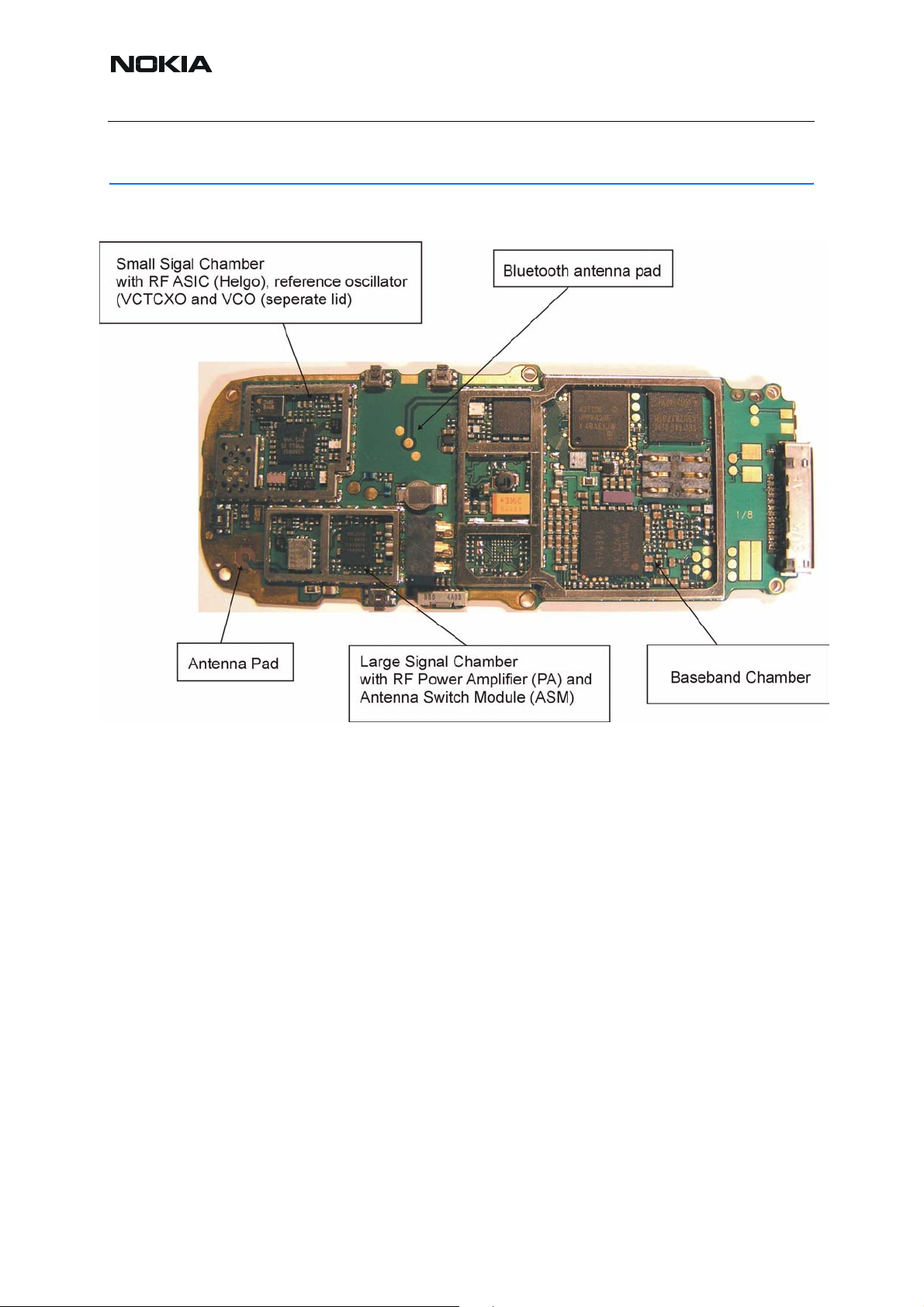
Printed Wiring Board
Figure 16:Assembled PWB with shielding chambers
40 COMPANY CONFIDENTIAL Issue 1 04/2005
Copyright © 2005 Nokia. All Rights Reserved.
Page 41

RM-94
7 - System Module Nokia Customer Care
■ RF key component placement
Figure 17:Placement of RF key components
Issue 1 04/2005 COMPANY CONFIDENTIAL 41
Copyright © 2005 Nokia. All Rights Reserved.
Page 42

RM-94
Nokia Customer Care 7 - System Module
List of RF key components:
Position Component Name
Z7800 Antenna Switch Module ASM
Z7802 SAW1800 RX
Z7801 SAW1900 RX
N7500 RF ASIC (Helgo 8.5)
V7800 LNA 1900 RX
G7501 VCTCXO
G7500 VCO
N7700 TX-PA
Z7803 SAW900 RX
Z7700 SAW900 TX
42 COMPANY CONFIDENTIAL Issue 1 04/2005
Copyright © 2005 Nokia. All Rights Reserved.
 Loading...