

Page 1

Nokia Customer Care
4 - Service Tools
Issue 1 03/2005 COMPANY CONFIDENTIAL
Copyright © 2005 Nokia. All Rights Reserved.
Page 2

RM-31
Nokia Customer Care 4 - Service Tools
This page has been intentionally left blank.
2 COMPANY CONFIDENTIAL Issue 1 03/2005
Copyright © 2005 Nokia. All Rights Reserved.
Page 3

RM-31
4 - Service Tools Nokia Customer Care
Table of Contents
Page No
Service Tools....................................................................................................... 5
List of service tools ............................................................................................ 5
JVB-1 Docking Station with DA-16 Docking Station Adapter............................. 7
DA-16 Docking Station Adapter ......................................................................... 8
SA-25 Antenna Coupler ..................................................................................... 9
SF-17 CCS POS Flash Adapter....................................................................... 14
MJ-22 Module Repair Jig ................................................................................. 15
RJ-66 Soldering Jig.......................................................................................... 18
SS-42 Camera Removal Tool .......................................................................... 19
ST-11 PA Rework Stencil ................................................................................ 20
Rework procedure............................................................................................ 21
RJ-46 Antenna Switch Rework Jig................................................................... 23
ST-15 / ST-31 Antenna Switch Solder Paste Stencil ....................................... 23
FPS-8 Flash Prommer ..................................................................................... 24
FPS-11 Multiprommer...................................................................................... 25
ACF-8 Universal Power Supply ....................................................................... 25
FLC-2 DC Cable .............................................................................................. 26
AXS-4 Service Cable ....................................................................................... 26
XCS-1 Service Cable ....................................................................................... 27
SW Security Device PKD-1.............................................................................. 27
FLS-4S POS (Point Of Sale) Flash Device (Sales Pack) ............................... 28
PCS-1 Power Cable......................................................................................... 28
CA-41 Power Supply Cable ............................................................................. 29
XRF-1 RF Cable .............................................................................................. 29
DAU-9S MBUS Cable ...................................................................................... 30
SCB-3 DC Cable.............................................................................................. 30
XCS-4 Modular Cable ...................................................................................... 31
CA-5S Service Battery Cable........................................................................... 31
CA-10DS Bi-directional Parallel Cable............................................................. 33
DAU-9T Service Cable..................................................................................... 33
Issue 1 03/2005 COMPANY CONFIDENTIAL 3
Copyright © 2005 Nokia. All Rights Reserved.
Page 4

RM-31
Nokia Customer Care 4 - Service Tools
This page has been intentionally left blank.
4 COMPANY CONFIDENTIAL Issue 1 03/2005
Copyright © 2005 Nokia. All Rights Reserved.
Page 5
RM-31
4 - Service Tools Nokia Customer Care
Service Tools
■ List of service tools
The table below gives a short overview of service tools that can be used for testing, error analysis and repair of product RM-31, refer to various set-ups.
Type
Designator
Programme Specific Tools
MJ-22 Module Jig
SF-17 POS flash adapter
DA-16 Docking Station Adapter
SA-25 RF coupler
RJ-66 PWB Soldering Rework Jig
ST-11 uPA Solder Paste Stencil
RJ-46 Antenna Switch Rework Jig
ST-15 Antenna Switch Solder Paste Stencil (BOM2)
ST-31 Antenna Switch Solder Paste Stencil (BOM1)
Common Service Tools
RJ-21 uPA Rework Jig
Description
SS-42 Camera removal tool (replaces SRT-10)
JBV-1 Docking Station
FLS-4S POS flash dongle E&A
FLS-4S POS flash dongle APAC
FLS-4S POS flash dongle US
FPS-8 Flash Box
XCS-1 Service Cable
XCS-4 Service Cable
PCS-1 Power Supply Cable
CA-41 Power Supply Cable
CA-5S Service Battery Cable
DAU-9S Service Cable
Issue 1 03/2005 COMPANY CONFIDENTIAL 5
Copyright © 2005 Nokia. All Rights Reserved.
Page 6
RM-31
Nokia Customer Care 4 - Service Tools
Type
Designator
XRF-1 RF-MEAS. CABLE/DCS1900
FPS-11 Multiprommer
ACF-8 Universal Power supply
AXS-4 D9-D9 serial cable
FLC-2 DC cable
CA-10DS Bi-directional parallel cable
PKD-1 Software protection key
SCB-3 DC-Cable
SPS-2 Solder paste spreader
DAU-9T Service cable (for testing phone with Xpress-on
funshell)
Programme Specific Service Tool spare parts
10pcs 2A fuse for MJ-22 module jig
Description
10pcs Test pins for MJ-22 module jig
10pcs Test pins for MJ-22 module jig
1pc Wing screw M3x20 for MJ-22 module jig
10pcs Test pins for SF-17 POS flash adaptor
10pcs Flash interface pins for DA-16 docking station adaptor
10pcs SIM interface pins for DA-16 docking station adaptor
6 COMPANY CONFIDENTIAL Issue 1 03/2005
Copyright © 2005 Nokia. All Rights Reserved.
Page 7

RM-31
4 - Service Tools Nokia Customer Care
■ JVB-1 Docking Station with DA-16 Docking Station Adapter
The JVB-1 docking station has been designed for calibration and software update use. The DA16 docking station adapter makes signal connections to the phone. JVB-1 and DA-16 are used
as one unit.
JVB-1 main electrical functions include the following:
• adjustable VBATT calibration voltage, current measurement limit voltage
“VCHAR”, current measurement calibration “ICHAR”
• adjustable ADC calibration voltage via BTEMP and BSI signal
• BTEMP and BSI calibration resistor
• signals from FBUS to the phone via parallel jig
• control via FBUS or USB
• Flash OK/FAIL indication
In calibration mode JVB-1 is powered by external power supply 11-16V DC. In flashing power
for the phone can be taken from FPS-8 or external power supply 11-16V DC.
Issue 1 03/2005 COMPANY CONFIDENTIAL 7
Copyright © 2005 Nokia. All Rights Reserved.
Page 8
RM-31
Nokia Customer Care 4 - Service Tools
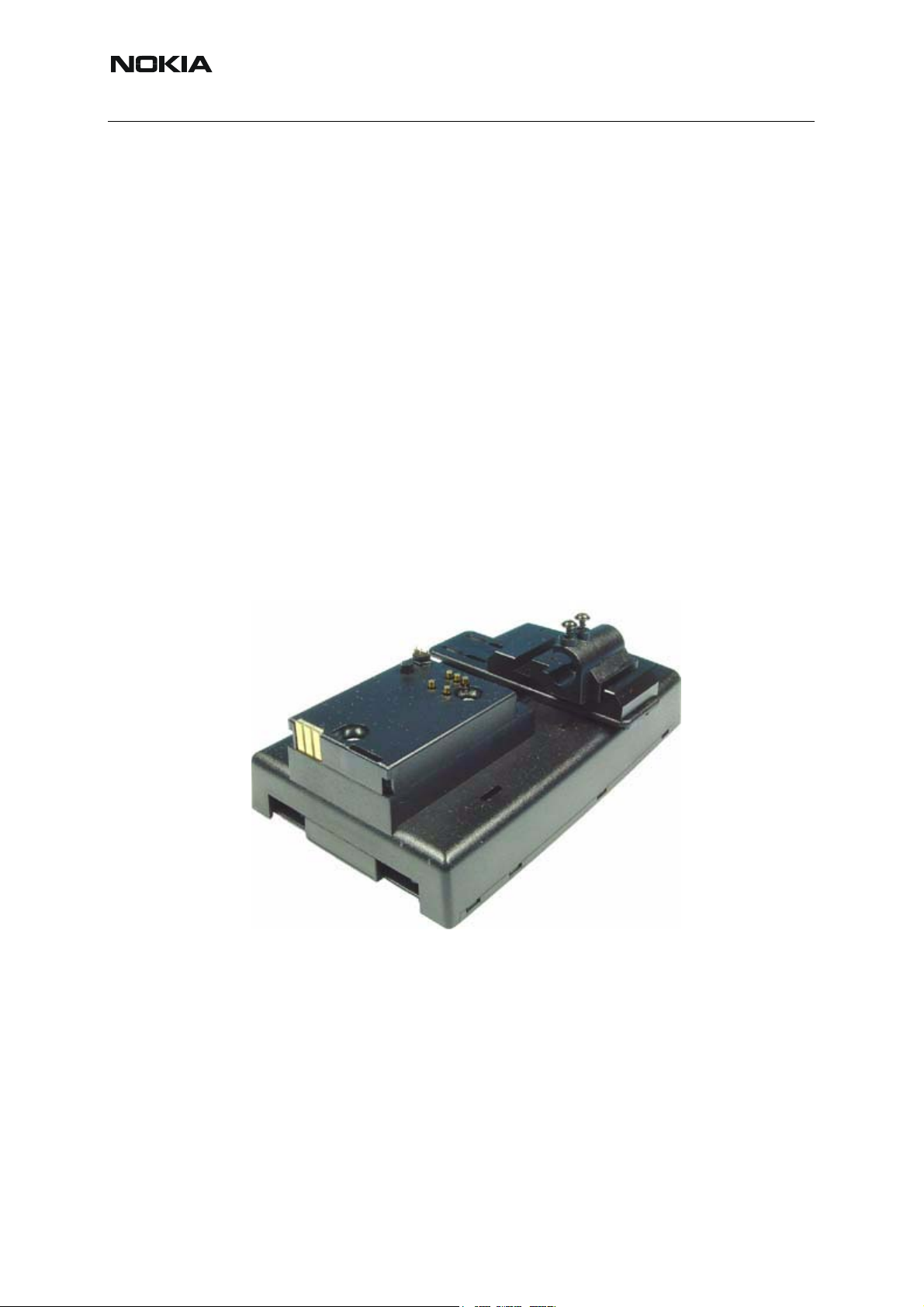
■ DA-16 Docking Station Adapter
Docking station adapter for assembled RM-31 phones. The docking station adapter supports
testing, flashing, energy management calibration. If used in conjunction with the RF-coupler
SA-25, also RF function testing is possible.
Features include:
• compatible for JBV-1
• easy phone attachment and detachment
• reliable phone locking
• switch for reliable detection of phone attachment
• replaceable test pins
• internal SIM holder with interface to phone SIM reader
Spare parts:
• Flash interface pins (10pcs)
• SIM interface pins (10pcs)
View of DA-16
8 COMPANY CONFIDENTIAL Issue 1 03/2005
Copyright © 2005 Nokia. All Rights Reserved.
Page 9
RM-31
4 - Service Tools Nokia Customer Care
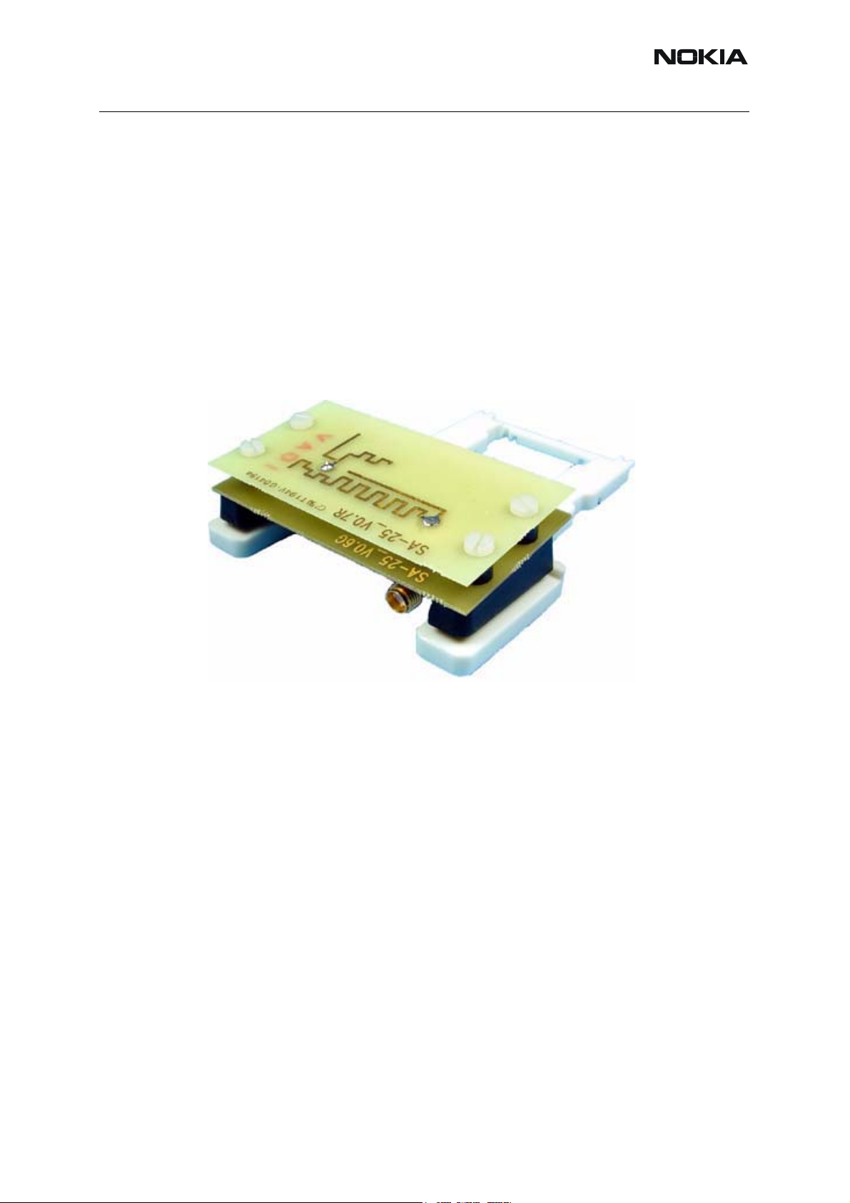
■ SA-25 Antenna Coupler
RF antenna coupler for use with the docking station adapter (DA-16).
Extends the docking station adapter to allow RF function tests in GSM bands 850, 900, 1800
and 1900 MHz.
Features include:
• easy attachment to DA-16 without use of tools
• reliable RF connection to phone module under test
• low attenuation and small “ripple” over the width of each GSM band
View of SA-25
Issue 1 03/2005 COMPANY CONFIDENTIAL 9
Copyright © 2005 Nokia. All Rights Reserved.
Page 10
RM-31
Nokia Customer Care 4 - Service Tools
Installing instructions for RF coupler to docking station adapter
Open the housing by pressing the housing apart. Now you can remove the bottom plate of the
docking station adapter.
10 COMPANY CONFIDENTIAL Issue 1 03/2005
Copyright © 2005 Nokia. All Rights Reserved.
Page 11

RM-31
4 - Service Tools Nokia Customer Care
Remove the four screws fixing the PWB by using Torx T6 screw driver. These screws are too
short, therefore four longer screws are delivered together with the coupler.
Install the coupler and use the new screws.
Issue 1 03/2005 COMPANY CONFIDENTIAL 11
Copyright © 2005 Nokia. All Rights Reserved.
Page 12

RM-31
Nokia Customer Care 4 - Service Tools
Close the docking station adapter by attaching the bottom plate.
Ready.
Attenuation table for antenna coupler SA-25 V0.7
Docking station antenna coupler SA-25_V0.7 attenuation table for 6020, measured with Universal Radio Communication Tester CMU-200.
Docking station antenna coupler SA-25_V0.7 attenuation table for RM-30 and RM-31, measured with Universal Radio Communication Tester CMU-200
12 COMPANY CONFIDENTIAL Issue 1 03/2005
Copyright © 2005 Nokia. All Rights Reserved.
Page 13

RM-31
4 - Service Tools Nokia Customer Care
Table 1: RM-31
System Channel Tx-att. (dB) Rx-att. (dB)
GSM 850 128 5.4 5
190 4.7 6
251 4.9 6
GSM 1800 512 8.3 9
698 9 9
885 8.8 8
GSM 1900 512 8.8 9
700 8.2 9
810 8 8
Table 2: RM-30
System Channel Tx-att. (dB) Rx-att. (dB)
EGSM 900 975 4.9 5
38 5.3 6
124 5.9 7
GSM 1800 512 4.9 5
698 4.7 5
885 4.5 5
GSM 1900 512 4.8 6
700 4.9 6
810 4.9 6
Tx-attenuation tolerance is +/-0.5 dB.
Rx-attenuation tolerance is +/-1.0dB.
Issue 1 03/2005 COMPANY CONFIDENTIAL 13
Copyright © 2005 Nokia. All Rights Reserved.
Page 14

RM-31
Nokia Customer Care 4 - Service Tools
■ SF-17 CCS POS Flash Adapter
Point of sales flash adapter for RM-31 phones.
SF-17 establishes a simple environment for SW update purposes and connects to the same
flash test pattern and the phone battery contacts.
Features include:
• flashing and testing of the attached phone
• overvoltage and reverse polarity protection of adapter and attached phone
• green LED: power supply valid and attached to the phone (3.5V<Vcc<7V)
• red LED: overvoltage condition, phone power supply disconnected (Vcc>7V)
• shielded 10-pin Western connector towards flash equipment or PC
• 3mm DC-jack for phone and adapter power supply
• phone battery contacts (VCC, GND, BSI)
• flash test pattern pins
View of SF-17
Spare Parts
There are no serviceable parts inside SF-17, and SF-17 is not designed for disassembly. Only
serviceable part are the spring loaded test pins that can be replaced without soldering and disassembly. Used test pin type is SX-1-J-2.0-G from manufacturer IDI.
Bent pins can be extracted from adapter’s receptacle using a tool. Torn off pins can be replaced
using a slowly spinning 0.8 mm. For more detail, please refer to the Service Tool Troubleshooting section.
Test pins (10pcs / plastic bag)
14 COMPANY CONFIDENTIAL Issue 1 03/2005
Copyright © 2005 Nokia. All Rights Reserved.
Page 15

RM-31
4 - Service Tools Nokia Customer Care
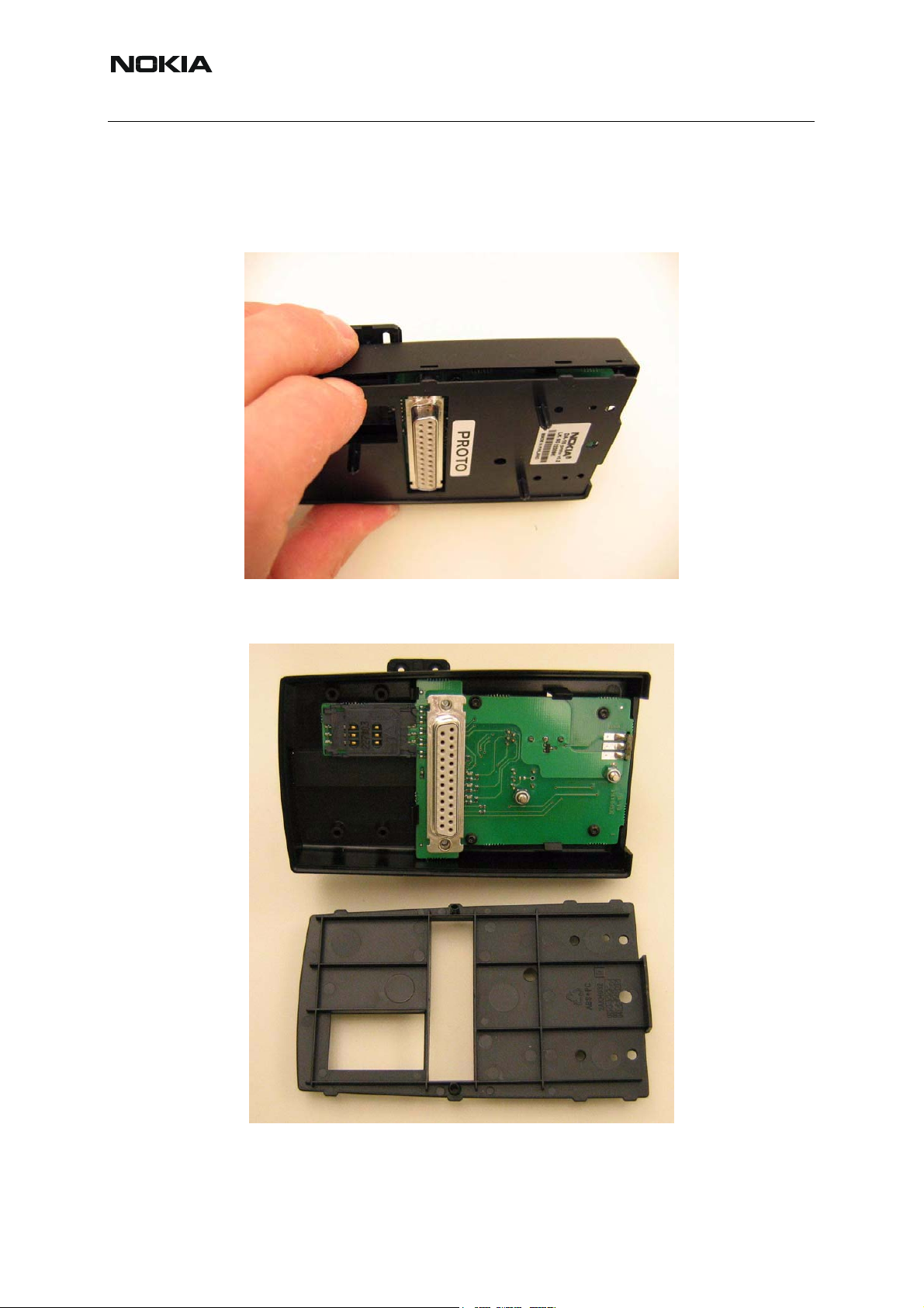
■ MJ-22 Module Repair Jig
Repair Jig for RM-31 phone module that allows full phone function.
General features include:
• easy phone module insertion and removal, proven jig locking mechanism
• ESD-proof base material and jig design
• unlimited operation of a disassembled phone module
• unrestricted access to phone module components
• access to system connector for accessory testing
• jig SIM holder with interface to phone SIM reader
• the installed UI module on the module jig allows key and display function test
• microphone, ear speaker and integrated handsfree speaker supplied on jig for
testing
• LOCAL/NORMAL switch
• access to phone module POWER-ON push-button
• quick and easy repair of jig components
View of MJ-22
Issue 1 03/2005 COMPANY CONFIDENTIAL 15
Copyright © 2005 Nokia. All Rights Reserved.
Page 16

RM-31
)
Nokia Customer Care 4 - Service Tools
Module repair jig MJ-22 update
The module repair jig MJ-22 needs to be updated because the holder can touch the soldering
point of the switch and cause mechanical stress (3).
(3)
Remove a small part of the press pad (2) with a simple file (1).
Power supply features
• jig and phone power supply via 3mm DC jack, fuse
• power stabilization and voltage regulator on jig (can be bypassed by jumper)
• reverse and over-voltage protection of jig and phone module
Communication and status LED’s
• green: Power supply
• green: MBUS activity
• orange: FBUS activity
(1)
(2)
(2
• jumper to disable LED’s for precise phone module current consumption measurements
Spare parts
• spring loaded test pins (used in upper part, can be replaced by soldering)
Test pins (10pcs / plastic bag)
16 COMPANY CONFIDENTIAL Issue 1 03/2005
Copyright © 2005 Nokia. All Rights Reserved.
Page 17

RM-31
4 - Service Tools Nokia Customer Care
• both ends spring loaded test pin (used in lower part, can be replaced by hand after
disassembly of lower PCB)
Test pins (10pcs / plastic bag)
• fuse inside holder
Fuses (10 pcs)
•wing screw M3x20
Replacement part (1pc)
Usage hints
• Before first use, verify setting of power supply jumper on the rear (=bottom PCB)
of the jig; if power supply is >4.2 V, make sure jumper enables power regulation of
the jig in order to prevent overvoltage for the phone module under test and the jig.
• In case of flashing problems in the jig, verify the switch on the upper part of the
jig is in position “Flash”; position “Accessory” is intended for ACI tests with connected
ACI-communication enabled accessories, such as car kits or camera headsets.
• FM ANT (X7) is not applicable for RM-31.
• On left hand side there is a slit for IrDa.
• When shielding lids are removed from the shielding frame on the PWB, new
shielding lids must be used for proper closing of the shielding. It is not allowed to reuse the removed ones.
Issue 1 03/2005 COMPANY CONFIDENTIAL 17
Copyright © 2005 Nokia. All Rights Reserved.
Page 18

RM-31
Nokia Customer Care 4 - Service Tools
■ RJ-66 Soldering Jig
Soldering jig is used for module level repair, either as fixation in µBGA rework places or when
there is need to hold a module on the work bench for any other repair. The soldering jig is also
usable for RH-37, RH-49, RM-17 and RM-31.
Features include:
• convenient locking mechanism
• four (optional mount) rubber feet allow usage also on repair benches
• fixation of phone module in both ways possible (bottom or top side up)
• ESD proof material
• standard uBGA jig thickness and outer dimensions
View of RJ-66
18 COMPANY CONFIDENTIAL Issue 1 03/2005
Copyright © 2005 Nokia. All Rights Reserved.
Page 19

RM-31
4 - Service Tools Nokia Customer Care
■ SS-42 Camera Removal Tool
Used to unlock and lift out camera module.
Note: Replaces SRT-10 which can only be used for unlocking.
View of SS-42
Issue 1 03/2005 COMPANY CONFIDENTIAL 19
Copyright © 2005 Nokia. All Rights Reserved.
Page 20

RM-31
Nokia Customer Care 4 - Service Tools
■ ST-11 PA Rework Stencil
The PA rework stencil is reused from RH-23.
SK-9 PA rework kit
containing
RJ-21 PA rework jig
(designed for RH-23 and RM-31)
ST-11 PA rework stencil
(designed for RH-23)
If spreader is needed, please refer to
SPS-2 Spreader
Note: For RM-31, another stencil than the one included in the rework kit SK-9 is needed, because another PWB pad layout is used. Therefore, ensure that for RM-31 the stencil ST-11 is
used for PA repairs.
20 COMPANY CONFIDENTIAL Issue 1 03/2005
Copyright © 2005 Nokia. All Rights Reserved.
Page 21

RM-31
4 - Service Tools Nokia Customer Care
■ Rework procedure
Due to the large mechanical tolerance of the power amplifiers, the following procedure is necessary:
1. Put the power amplifier into the RJ-21 rework jig. The PA should be placed in
the best fit location, this is determined by placing it in the largest location first, if
this is to large reposition the PA in the next size location. This should be carried
out until the best fit location is found.
1. Once the best fit location has been found, leave the PA there and put the stencil
on top of the jig and PA.
2. Put soldering paste on the PA properly.
Issue 1 03/2005 COMPANY CONFIDENTIAL 21
Copyright © 2005 Nokia. All Rights Reserved.
Page 22

RM-31
Nokia Customer Care 4 - Service Tools
3. Remove the stencil and the PA from the jig.
4. Start the soldering process.
22 COMPANY CONFIDENTIAL Issue 1 03/2005
Copyright © 2005 Nokia. All Rights Reserved.
Page 23

RM-31
4 - Service Tools Nokia Customer Care
■ RJ-46 Antenna Switch Rework Jig
View of RJ-46
■ ST-15 / ST-31 Antenna Switch Solder Paste Stencil
• ST-15 Antenna Switch Solder Paste Stencil
Note: ST-15 is only usable for BOM2 and for ASM from Murata.
• ST-31 Antenna Switch Solder Paste Stencil
Note: ST-31 is only usable for BOM1 and for ASM from Hitachi.
View of ST-15 and ST-31
Issue 1 03/2005 COMPANY CONFIDENTIAL 23
Copyright © 2005 Nokia. All Rights Reserved.
Page 24

RM-31
Nokia Customer Care 4 - Service Tools
■ FPS-8 Flash Prommer
The flash prommer FPS-8 is used with e.g. docking station (+adapter) or the POS flash adapter.
Power is supplied to FPS-8 from the universal power supply.
The sales pack includes the following hardware items:
• FPS-8 Flash Prommer
• ACF-8 Universal Power Supply
• AXS-4 Service Cable (D9-D9)
• CA-10DS Bi-directional Parallel Cable
View of FPS-8
24 COMPANY CONFIDENTIAL Issue 1 03/2005
Copyright © 2005 Nokia. All Rights Reserved.
Page 25
RM-31
4 - Service Tools Nokia Customer Care
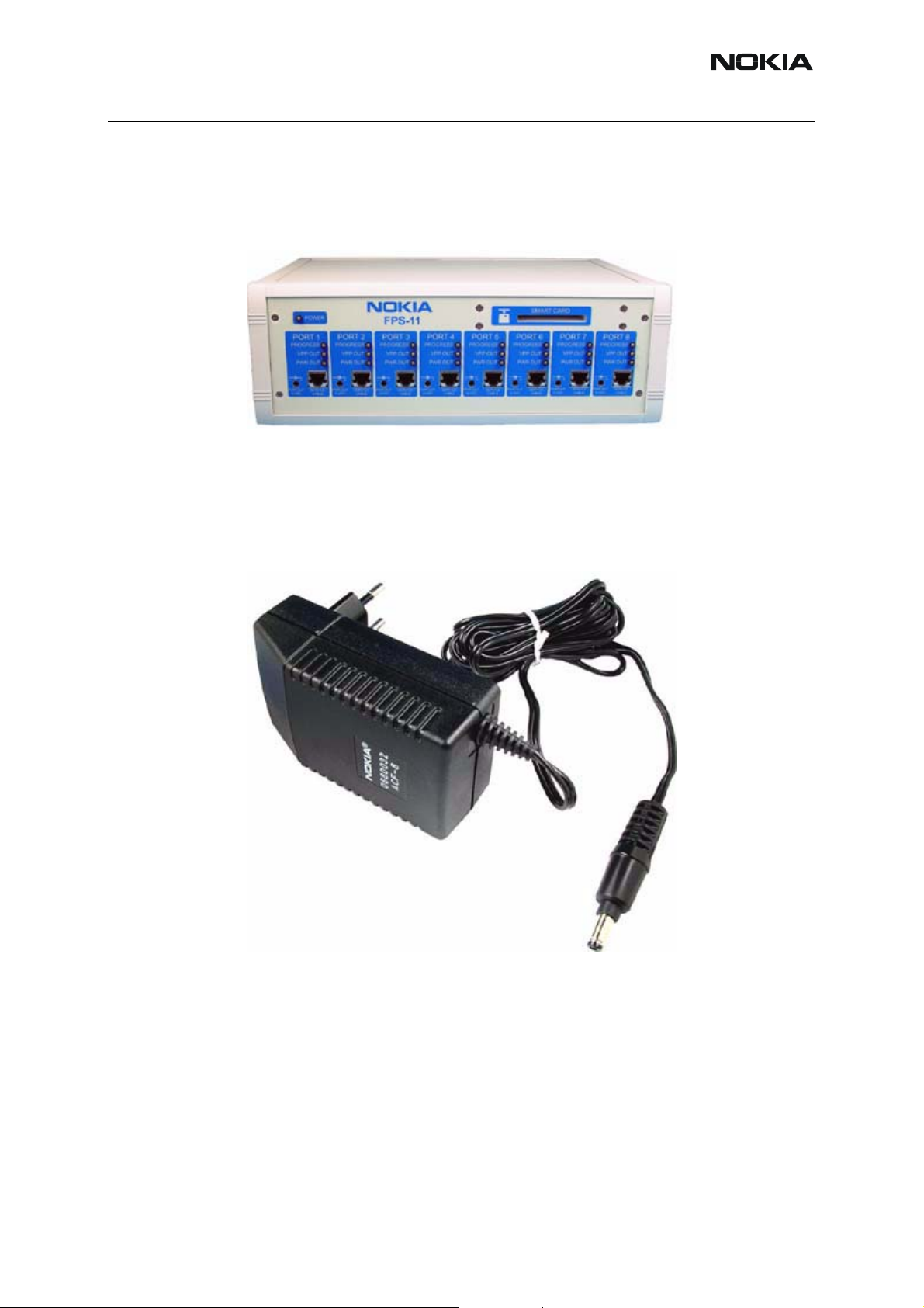
■ FPS-11 Multiprommer
View of FPS-11
■ ACF-8 Universal Power Supply
ACF-8 universal power supply is used to power FPS-8. ACF-8 has 6 V DC and 2.1 A output.
View of ACF-8
Issue 1 03/2005 COMPANY CONFIDENTIAL 25
Copyright © 2005 Nokia. All Rights Reserved.
Page 26

RM-31
Nokia Customer Care 4 - Service Tools
■ FLC-2 DC Cable
The FLC-2 is used to supply a controlled operating voltage.
View of FLC-2
■ AXS-4 Service Cable
The AXS-4 D9-D9 service cable is used to connect two 9 pin D connectors e.g. between PC
and FPS-8. Cable length is 2 meters.
View of AXS-4
26 COMPANY CONFIDENTIAL Issue 1 03/2005
Copyright © 2005 Nokia. All Rights Reserved.
Page 27

RM-31
4 - Service Tools Nokia Customer Care
■ XCS-1 Service Cable
The XCS-1 service cable is used to connect FLS-4 to SF-17.
View of XCS-1
■ SW Security Device PKD-1
SW security device is a piece of hardware enabling the use of the service software when connected to the parallel (LPT) port of the PC. Without the dongle present it is not possible to use
the service software. Printer or any such device can be connected to the PC through the dongle
if needed.
Caution: Make sure that you have switched off the PC and the printer before
making connections!
Caution: Do not connected the PKD-1 to the serial port. You may dam age your
PKD-1!
View of SW Security Device
Issue 1 03/2005 COMPANY CONFIDENTIAL 27
Copyright © 2005 Nokia. All Rights Reserved.
Page 28

RM-31
Nokia Customer Care 4 - Service Tools
■ FLS-4S POS (Point Of Sale) Flash Device (Sales Pack)
FLS-4S is a dongle and flash device incorporated into one package, developed specifically for
POS use.
View of FLS-4S
■ PCS-1 Power Cable
The PCS-1 power cable (DC) is used to connect e.g. JVB-1 to FPS-8.
View of PCS-1
28 COMPANY CONFIDENTIAL Issue 1 03/2005
Copyright © 2005 Nokia. All Rights Reserved.
Page 29

RM-31
4 - Service Tools Nokia Customer Care
■ CA-41 Power Supply Cable
Power supply cable (e.g. FPS-10 to JBV-1).
View of CA-41
■ XRF-1 RF Cable
RF cable XRF-1 is used to connect e.g. module jig to RF measurement equipment.
View of XRF-1
Issue 1 03/2005 COMPANY CONFIDENTIAL 29
Copyright © 2005 Nokia. All Rights Reserved.
Page 30

RM-31
Nokia Customer Care 4 - Service Tools
■ DAU-9S MBUS Cable
The MBUS cable DAU-9S has a modular connector, and is used with between PC's serial port
and e.g. module jig.
View of DAU-9S
■ SCB-3 DC Cable
The DC cable SCB-3 is used to connect e.g. JVB-1 to the phone.
View of SCB-3
30 COMPANY CONFIDENTIAL Issue 1 03/2005
Copyright © 2005 Nokia. All Rights Reserved.
Page 31

RM-31
4 - Service Tools Nokia Customer Care
■ XCS-4 Modular Cable
XCS-4 is a shielded cable (one specially shielded conductor) modular cable for flashing and
service purposes.
View of XCS-4
■ CA-5S Service Battery Cable
Charger plug to charger plug service cable.
View of CA-5S
Issue 1 03/2005 COMPANY CONFIDENTIAL 31
Copyright © 2005 Nokia. All Rights Reserved.
Page 32

RM-31
Nokia Customer Care 4 - Service Tools
■ CA-10DS Bi-directional Parallel Cable
Bi-Directional parallel cable included in FPS-8 sales pack.
View of CA-10DS
■ DAU-9T Service Cable
Pop-PortTM to D9 connector service cable, used for testing correct operation of phone and
XPress-on Funshell.
View of DAU-9T
32 COMPANY CONFIDENTIAL Issue 1 03/2005
Copyright © 2005 Nokia. All Rights Reserved.
 Loading...