

Page 1

Nokia Customer Care
6015/6015i/6016i/6019i (RH-55),
6012 (RM-20) Series Transceivers
System Module
Issue 1 - Revision 002 09/2004 Company Confidential ©2004 Nokia Corporation
Page 2

6015/6015i/6016i/6019i (RH-55), 6012 (RM-20)
System Module Nokia Customer Care
Contents Page
Introduction ..................................................................................................................................................... 3
Operational Modes ...................................................................................................................................... 4
Engine Module .............................................................................................................................................6
Environmental Specifications................................................................................................................ 6
Temperature Conditions.......................................................................................................................... 6
Baseband Module ........................................................................................................................................6
UEM .............................................................................................................................................................. 7
BB-RF Interface Connections .................................................................................................................10
UPP............................................................................................................................................................. 16
Memory..................................................................................................................................................... 16
User Interface Hardware .........................................................................................................................17
LCD............................................................................................................................................................. 17
Keyboard................................................................................................................................................... 17
Power Key ................................................................................................................................................ 18
Phone Keys............................................................................................................................................... 18
Lights......................................................................................................................................................... 18
Vibra .......................................................................................................................................................... 18
Audio Hardware .........................................................................................................................................19
Earpiece .................................................................................................................................................... 19
Microphone ............................................................................................................................................. 19
MIDI Speaker........................................................................................................................................... 19
Battery ..........................................................................................................................................................20
Battery Connector ................................................................................................................................. 20
Accessories Interface ................................................................................................................................21
System Connector.................................................................................................................................. 21
Charger IF................................................................................................................................................. 24
Test Interfaces ............................................................................................................................................24
Production Test Pattern ....................................................................................................................... 24
General Testing Information............................................................................................................... 28
RF Module ....................................................................................................................................................28
Temperature Conditions....................................................................................................................... 28
Main Technical Characteristics.......................................................................................................... 29
Antenna .................................................................................................................................................... 29
Transmitter Block Diagram ................................................................................................................. 30
Synthesizer .............................................................................................................................................. 32
Receiver ........................................................................................................................................................35
GPS Engine .................................................................................................................................................... 37
Page 2 ©2004 Nokia Corporation Company Confidential Issue 1 - Revision 002 09/2004
Page 3

6015/6015i/6016i/6019i (RH-55), 6012 (RM-20)
Nokia Customer Care System Module
Introduction
Following is a summary of the 6015/6015i/6016i/6019i, and 6012 transceivers:
Model Type Technology Memory
6012 RM-20 Analog and CDMA IS2000 Discrete
Flash: 64 Mb
SRAM: 4 Mb
6015 RH-55 Analog and CDMA IS2000 Discrete
Flash: 64 Mb
SRAM: 4 Mb
6015i RH-55 Analog and CDMA IS2000 Combo
Flash: 64 Mb
SRAM: 16 Mb
6016i RH-55 Analog and CDMA IS2000 Combo
Flash: 64 Mb
SRAM: 16 Mb
6019i RH-55 Analog and CDMA IS2000 Combo
Flash: 128 Mb
SRAM: 16 Mb
Frequency
(MHz)
800 No
800/1900 No
800/1900 Yes
800/1900 Yes
800/1900 Yes
GPS Module
All models include a whip antenna and a planar inverted F antenna (PIFA). When the
whip antenna is in, only the PIFA antenna is active. When the whip is extended, both
antennas are active. Access for testing cellular and GPS engines is possible once the
A-cover is removed.
Phone features include the following:
• Internal vibra
• High-resolution display (96x65 pixels)
• 2.5 mm Universal headset connector with TTY/TDD support
• GPS technology (6015i, 6016i, 6019i)
• T9 predictive text input
• Voice dialing
• Two-way, hands-free speakerphone
• 16-polyphonic MIDI speaker
• High speed data (HSD) support (up to 153 Kbps)
• 4-way scroll design
• User changeable front and back cover
• Openwave 4.1 Web minibrowser (network dependant)
Issue 1 - Revision 002 09/2004 ©2004 Nokia Corporation Company Confidential Page 3
Page 4
6015/6015i/6016i/6019i (RH-55), 6012 (RM-20)
System Module Nokia Customer Care
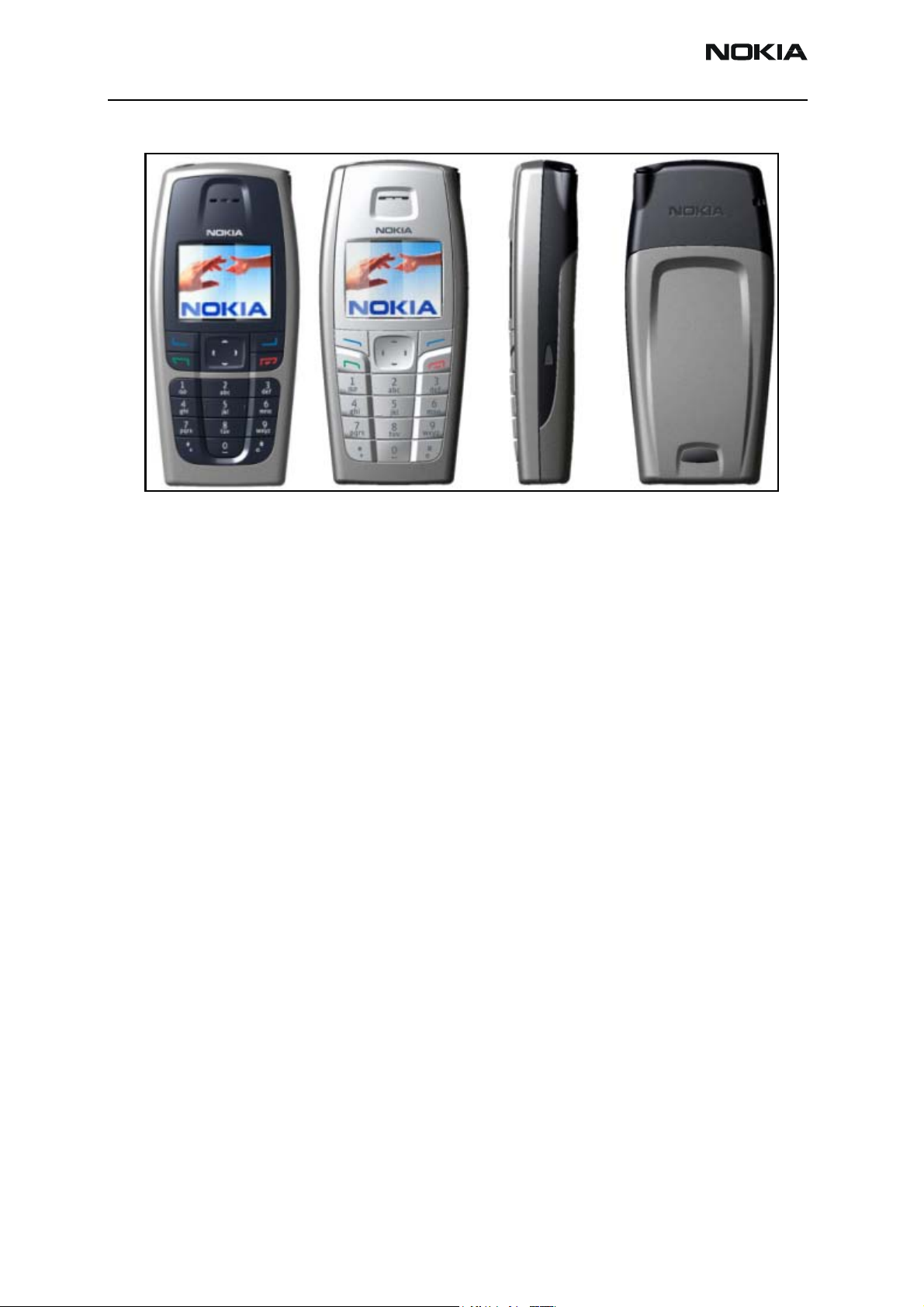
Note: The 6016i (left) has a unique A-cover assembly
Operational Modes
There are several different operational modes, which have different states controlled by
the cellular SW. Some examples are: Idle State (on ACCH), Camping (on DCCH), Scanning,
Conversation, and No Service Power Save (NSPS).
• Power-off mode = Only the circuits needed for power-up are supplied.
• Sleep mode = Circuits are powered down and only the 32kHz sleep clock runs. In
slotted mode or idle mode (a combination of sleep mode and receive mode), some
circuits turn on during the wake-up slot to receive page messaging from the base
station.
• Active mode = All circuits are supplied with power, although some parts might be
in idle state part of the time.
• Charge mode = Effective in parallel with all previous modes. The charge mode
itself consists of two different states, the fast charge and the maintenance mode.
• Local mode = Used for alignment and testing.
Page 4 ©2004 Nokia Corporation Company Confidential Issue 1 - Revision 002 09/2004
Page 5

6015/6015i/6016i/6019i (RH-55), 6012 (RM-20)
Nokia Customer Care System Module
V1A, V1B 4.60 - 4.90 vdc
V2 - V7 2.70 - 2.86 vdc
VIO 1.72 - 1.88 vdc
External
Antenna
1900 MHz
PCS Duplexer
A
B
850 MHz
Cellular
Duplexer
TX: 824 - 849 MHz
BT Front
EndBTReceiver
GPS
Front End
RX: 1930 - 1990 MHz
TX: 1859 - 1910 MHz
RX: 869 - 894 MHz
Vbatt
Vbatt
PA
GPS
Receiver
ST PAC
VR 5
2058.1-2118.1 MHz
997.11-1022.52MHz
Temp Sensor
50 KHz Steps
30KHz Steps
VR1B
UHF
PLL
TX Gate
PA Bias
Enable
PA Bias
DAC
20
PCS
20 35
Cellular
4 GHz
Grey/dashed lines are backups or options
BB 4.0
128.1MHz
BW=30 KHz
128.1MHz
AGC2
LO
SYNTH LE
Power Detector
35
Charge PumpLPF
BAND
SEL
JUPITER
AGC1
35
+
Div 2
35
Div 4
+
4 GHz
UHF PLL
Apollo 2 Top Level
BB4.0 BB4.5 BB5.0
UPP8MV3 TIKU_2G RAP_CDMA
UEM UEM TAHVO
RETU
NOKIA CONFIDENTIAL
DHAxxx-EN
18-Feb-03
VREFRF01
VR 5
VR 7 VI O
RX I
BatmanAlfred
IF/
Analog
Bias
3
DET_OUT
SIO
3
RX Q
VR3
F ref
VCTCXO
19.2 MHz
RF Bus
VIO (1.8V)
I_ref
6
TX I
TX Q
VR2
F ref
VR4
MIDI Speaker
MUX
HF
BuzzO
XEAR
Vibra
2
UEM UPP
RX_IP
RXI ADC
RX_IN
RX_QP
RXQ ADC
RX_QN
AUX Path
DAC
AFC DAC
AFC
PA TEMP
Slow ADC
PWROUT
TX_IP
TXI DAC
TX_IN
TX_QP
TXQ DAC
TX_QN
2
2
2
VSIM
SIMCLK
SIMCARDDECT
SIM Card
SIMDAIO
HF
ACI
Mic2
FBus
DCT3 or Tomahawk
bottom Connector
r
a
Mic1
E
2
2
VBAT
3
HeadInt
K-D Light/CalLED
BSI
VREFRF01
VREFRF02
I_PA1
I_PA2
2
PwrOnX
2.8-4.2v
VBat
BTemp
VBack
VR1
VR2
VR3
VR4
VR5
VR6
VR7
VIO
SIMIOCTRL
Keyb1/2
LS
VREFRF01
VREFRF02
OSC2
OSC1
VR1A
VR1B
VR2
VR3
VR4
VR5
VR6
VR7
VI0
SleepClk
CBus
3
DBus
3
RFConvClk
TxIQD
2
RxIQD
2
AudioConv
2
UEMInt
PURX
AuxDa
MBus
2
FBus
2
IRTx/Rx
2
VCore
VIO
SleepX
SIMDAIO
SIMCLK
LCD/
Keypad
32 Khz
LCDCtrl
KeyB[10:0]
SYS_CLK
8MV3
PDMs
4
RF
Bus
GP I/O
8
3
11
ExtAd[23:16]
Flash
TX AGC 1
TX AGC 2
RF_CLK
RF_DATA
RF_ENX
RESETX
AGC_UP_DN
AGC_CLK
PA_D(2:0)
TX_GATE
9
16
FlsCtrl
ExtAdDa[15:0]
TX AGC
1
TX AGC
2
RF_CLK
RF_DATA
RF_ENX
RESET
X
STIBus
JTAG
DC-DC
Converter
RF Bus
3
7
VCore
(DC-DC)
Ostrich
Conn.
JTAG
Conn.
Figure 1: Interconnecting diagram
Issue 1 - Revision 002 09/2004 ©2004 Nokia Corporation Company Confidential Page 5
Page 6

6015/6015i/6016i/6019i (RH-55), 6012 (RM-20)
System Module Nokia Customer Care
Engine Module
Environmental Specifications
Normal and extreme voltages:
• Nominal battery voltage: 3.6 V
• Maximum battery voltage: 4.5 V
• Minimum battery voltage: 3.2 V
Temperature Conditions
Following are the temperature ranges for the engine:
o
• Ambient temperature: -30 to +60
C
• PWB temperature: -30 to +85
Baseband Module
The core part of the baseband module consists of the following ASICs:
•UEM
•UPP
• Flash memory
The following sections describe these parts.
o
C
Page 6 ©2004 Nokia Corporation Company Confidential Issue 1 - Revision 002 09/2004
Page 7

6015/6015i/6016i/6019i (RH-55), 6012 (RM-20)
Nokia Customer Care System Module
PA Supply
RF Supplies
Apollo 2
BATTERY
RF RX/TX
RFIC CTRL 19.2 MHz
UEM
Ear
MIC
Buzzer
Vibra
MEMADDA
MEMCONT
FLASH
UPP
PURX
RF RX/TX
Sleep Clock 32 kHz
CBUS/DBUS
AUDIO
BB Supplies
UEM
External Audio
Charger
Connection
DCT4 System
Connector
Figure 2: Baseband module diagram
UEM is the Universal Energy Management IC for DCT4 digital handportable phones. In
addition to energy management, it performs all the baseband mixed-signal functions.
Most of UEM pins have 2kV ESD protection. Those signals that are considered to be
exposed more easily to ESD have 8kV protection inside UEM. Such signals are all audio
signals, headset signals, BSI, Btemp, Fbus, and Mbus signals.
Regulators
UEM has six regulators for baseband power supplies and seven regulators for RF power
supplies. VR1 regulator has two outputs VR1a and VR1b.
Bypass capacitor (1uF) is required for each regulator output to ensure stability.
Issue 1 - Revision 002 09/2004 ©2004 Nokia Corporation Company Confidential Page 7
Page 8

6015/6015i/6016i/6019i (RH-55), 6012 (RM-20)
System Module Nokia Customer Care
Reference voltages for regulators require external 1uF capacitors. Vref25RF is reference
voltage for VR2 regulator; Vref25BB is reference voltage for VANA, VFLASH1, VFLASH2,
VR1 regulators; Vref278 is reference voltage for VR3, VR4, VR5, VR6, VR7 regulators;
VrefRF01 is reference voltage for VIO, VCORE, VSIM regulators, and for RF.
The baseband is powered from five different UEM regulators:
Table 1: Baseband Regulators
Regulator
VCORE
DC/DC
VIO 150 1.8 Enabled always except during power-off mode
VFLASH1 70 2.78 Enabled always except during power-off mode
VFLASH2 40 2.78 Enabled only when data cable is connected
VANA 80 2.78 Enabled only when the system is awake (off during sleep
VSIM 25 3.0 Enabled during power-up mode and scanning for a SIM
Maximum
Current (mA)
300 1.35 The power-up default value is 1.35V. The output voltage is
Vout (V) Notes
selectable: 1.0V/1.3V/1.5V/1.8V.
and power-off modes)
card
Table 2 includes the UEM voltage regulators used by the RF.
Table 2: RF Regulators
Regulator
Maximum
Current (mA)
Vout (V) Notes
VR1A 10 4.75 Enabled when the receiver is on
VR1B 10 4.75 Enabled when the transmitter is on
VR2 100 2.78 Enabled when the transmitter is on
VR3 20 2.78 Enabled when SleepX is high
VR4 50 2.78 Enabled when the receiver is on
VR5 50 2.78 Enabled when the receiver is on
VR6 50 2.78 Enabled when the transmitter is on
VR7 45 2.78 Enabled when the receiver is on
Table 3: Regulator Descriptions
Regulator Description
VANA Supplies internal and external analog circuitry of the BB. This regulator is disabled in sleep mode.
Vflash1 Supplies the LCD and the digital parts of the UEM ASIC. This regulator is enabled during startup
and enters low Iq-mode in sleep mode.
Page 8 ©2004 Nokia Corporation Company Confidential Issue 1 - Revision 002 09/2004
Page 9

6015/6015i/6016i/6019i (RH-55), 6012 (RM-20)
Nokia Customer Care System Module
Table 3: Regulator Descriptions (Continued)
Regulator Description
VIO Supplies both external and internal logic circuitries. This regulator is used by the LCD, flash, Bat-
man, Jupiter, GPS RF, GPS Baseband, and the UPP. The VIO regulator enters low Iq mode in sleep
mode.
VCORE Supplies the DSP, the core part of the UPP, and the GPS BB ASIC. The voltage is programmable
and the startup default is 1.35V. This regulator enters low Iq-mode in sleep mode.
VR1 (VR1A, VR1B) Uses two LDOs and a charge pump. VR1A is used in the UHF PLL, and VR1B is used
for Jupiter PLL.
VR2 Linear regulator used to supply the Jupiter RF ASIC.
VR3 Linear regulator used by the VCTCXO circuitry.
VR4 Linear regulator used by the UHF PLL and the UHF VCO.
VR5 Linear regulator used by the Batman and Alfred ASICs.
VR6 Linear regulator used by the Jupiter PLL.
VR7 Linear regulator used by the Batman ASIC.
RF Interface
In addition to the RF regulators mentioned, UEM handles the interface between the
baseband and the RF section. It provides A/D and D/A conversion of the in-phase and
quadrature receive and transmit signal paths, and also A/D and D/A conversions of
received and transmitted audio signals to and from the UI section. The UEM supplies the
analog AFC signal to the RF section according to the UPP DSP digital control. It also
converts PA temperature into real data for the DSP. The UPP controls the RFIC through
the 3-wire RFIC bus. UPP also provides PDM regulator for RF interface (RX/TX AGC
control).
Charging Control
The CHACON block of the UEM controls charging. Needed functions for charging controls
include: PWM-controlled battery charging switch, charger-monitoring circuitry, and
battery voltage monitoring circuitry. In addition, external components are needed for
EMC protection of the charger input to the baseband module. The DCT4 baseband is
designed to electrically support both DCT3 and DCT4 chargers.
Digital Interface
Data transmission between the UEM and the UPP is implemented using two serial
connections, DBUS (9.6 MHz) for DSP and CBUS (1.2 MHz in CDMA) for MCU. UEM is a
dual-voltage circuit: the digital parts are running from 1.8V and the analog parts are
running from 2.78V. Vbat (3.6V) voltage regulators inputs also are used.
Audio Codec
The baseband supports two external microphone inputs and one external earphone
output. The inputs can be taken from an internal microphone, from a headset
microphone, or from an external microphone signal source through a headset connector.
Issue 1 - Revision 002 09/2004 ©2004 Nokia Corporation Company Confidential Page 9
Page 10

6015/6015i/6016i/6019i (RH-55), 6012 (RM-20)
System Module Nokia Customer Care
The output for the internal earpiece is a differential type output, and the differential
output is capable of driving 4Vpp to the earpiece with a 60 dB minimum signal to total
distortion ratio. Input and output signal source selection and gain control is performed
inside the UEM ASIC according to control messages from the UPP. Both a buzzer and an
external vibra alert control signals are generated by the UEM with separate PWM
outputs.
UI Drivers
The vibra, display LED, and keyboard LEDs are driven by open collector output drivers
inside UEM. These drivers can generate PWM square wave signals to these devices.
AD Converters
There is an 11-channel analog-to-digital converter in UEM. The AD converters are
calibrated in the production line.
BB-RF Interface Connections
All the signal descriptions and properties in the following tables are valid only for active
signals.
Signal
Name
RX_IF_AGC
Table 4: PDM Interface
From To Parameter Min Type Max Unit Function
Voltage Minimum 0.0 0.1 V Controls the gain
of the VGA and
mixer in the
receiver
SW-controlled
pulldown
UPP
GenIO
Batman
Voltage Maximum 1.75 1.8 1.86
Resolution 10 bits
Load resistance 1 Kohm
Load capacity 100 nf
Setting time 0.2 ms
Source impedance 200 Ohm
Step size 7.03 mV
Filter value 27
10
Polarity Decreasing PDM voltage increases the gain.
Reset state N/A Input,
kohm
nf
Clk Rate
(1)
9.6 19.2 MHz
Page 10 ©2004 Nokia Corporation Company Confidential Issue 1 - Revision 002 09/2004
Page 11

6015/6015i/6016i/6019i (RH-55), 6012 (RM-20)
Nokia Customer Care System Module
Table 4: PDM Interface (Continued)
Signal
Name
TX_AGC1
From To Parameter Min Type Max Unit Function
Voltage minimum 0.0 0.1 V Controls gain of
VGA in Jupiter
SW-controlled
pulldown
UPP
GenIO
Jupiter
Voltage maximum 1.75 1.8 1.86
Resolution 10 bits
Load resistance 1 Kohm
Load capacity 100 nf
Setting time 0.2 ms
Source impedance 200 Ohm
Step size 3.515 mV
Filter value 150
1
Polarity Decreasing PDM voltage increases the gain.
Reset state N/A Input,
kohm
nf
Clk rate 9.6 19.2 MHz
TX_AGC2 UPP
GenIO
Jupiter See the values for TX_AGC1.
Table 5: General I/O Interface
Signal From To Parameter
“1” TX Off 1.38 1.88
“0” TX On 0 0.4
Load resistance 1 220 Kohm
TX_Gate
UPP
GenIO
Jupiter
and PAs
Load capacity 20 pF
Timing accuracy Programmable
Reset state N/A, Input, Software-controlled
Drive capability 2.0 mA
Input Characteristics
Function
Min Type Max Unit
V
Punctures the PAs
and Jupiter ASIC
pull down
Issue 1 - Revision 002 09/2004 ©2004 Nokia Corporation Company Confidential Page 11
Page 12
6015/6015i/6016i/6019i (RH-55), 6012 (RM-20)
System Module Nokia Customer Care
Table 5: General I/O Interface (Continued)
Input Characteristics
Signal From To Parameter
Function
Min Type Max Unit
“0” 1.38 1.88
“1” 0 0.4
V
FastAGC
UPP
GenIO
RF/BB/I/F
Load resistance 1 Kohm
Load capacity 20 pF
Timing accuracy Controlled by the software
Drive capability 2.0 mA
Table 6: VCTCXO Interface
Controls the PDM
filter Time Constant
Signal From To Parameter Min Type Max Unit Function
Frequency 19.2 MHz High stability
clock signal for
logic circuits
AC-coupled sinewave.
Signal amplitude 0.5 1.0 1.5 Vpp
Input impedance 10 kohm
Input capacity 5 7 10 pF
2nd harmonic -20 dBc 0.2 Vpp amplitude
3rd harmonic -10 dBc 0.8 Vpp amplitude
19.2MHz VCTCXO
UPP
Batman
Jupiter
UHF PLL
GPS
Table 7: Regulated Supplies from UEM to RF
Signal
Name
VBAT Battery PA & UEM
VR1A UEM UHF PLL
From To Parameter Min Type Max Unit Function
4th harmonic -15 dBc 0.8 Vpp amplitude
Settling time
0-90% amplitude
Settling time
+/- 1 ppm
Voltage 3.04 3.5 4.2 V Battery supply.
Voltage 4.6 4.75 4.9 V Charge pump +
Current 5 mA
2
ms
3
Lithium only
linear regulator.
Can be used for
VCO varactor
control if 2.7V is
not enough.
Page 12 ©2004 Nokia Corporation Company Confidential Issue 1 - Revision 002 09/2004
Page 13

6015/6015i/6016i/6019i (RH-55), 6012 (RM-20)
Nokia Customer Care System Module
Table 7: Regulated Supplies from UEM to RF (Continued)
Signal
Name
VR1B UEM Jupiter PLL
VR2 UEM Jupiter
VR3 UEM
VR4 UEM
VR5 UEM
VR6 UEM Jupiter PLL
From To Parameter Min Type Max Unit Function
VCTCXO
and
19.2MHz
buffer
UHF PLL
and UHF
VCO
Batman/
Alfred
Voltage 4.6 4.75 4.9 V
Current 5 mA
Voltage 2.70 2.78 2.86 V 2.78 only (3.3V
Current 100 mA
Voltage 2.70 2.78 2.86 V
Current 20 mA
Voltage 2.70 2.78 2.86 V
Current 50 mA
Voltage 2.70 2.78 2.86 V
Current 50 mA
Voltage 2.70 2.78 2.86 V
Current 50 mA
SMPS not
enabled in UEM)
Low lq linear
regulator
Low lq linear
regulator
Low lq linear
regulator
Low lq linear
regulator
VR7 UEM Batman
VREFRF01 UEM
VREFRF02 UEM Not Used
VIO UEM
VRF_GPS
External
regulator
Batman
Vref
Jupiter
Batman
UHF PLL
GPS
GPS RF
Voltage 2.70 2.78 2.86 V
Current 30 mA
Output
impedance
Temp Coef -65 +65 uV/C
Voltage 1.334 1.35 1.366 V
Output
impedance
Temp Coef -65 +65 uV/C
Voltage 1.70 1.8 1.88 V
Voltage 2.7 2.78 2.86 V
Current 50 mA
10 ohm
10 ohm
Low noise linear
regulator
Voltage reference for RF-IC
1.2% accuracy
Voltage reference for RF-IC
1.2% accuracy
Supply for RF-BB
digital interface
and some digital
parts of RF
Supplies RF
section of GPS
Issue 1 - Revision 002 09/2004 ©2004 Nokia Corporation Company Confidential Page 13
Page 14

6015/6015i/6016i/6019i (RH-55), 6012 (RM-20)
System Module Nokia Customer Care
Table 8: RF-BB Analog Signals
Signal
Name
RX_IP/RX_IN Batman UEM
RX-QP/RX-QN Batman UEM See the values for RX_IP/RX_IN Differential quad-
TX_IP/TX_IN UEM Jupiter
From To Parameter Min Type Max Unit Function
Differential
voltage swing
(static)
DC level 1.3 1.35 1.4 V
Resolution 8 12 bits Depends on over-
Differential
input
impedance
Differential
voltage swing
DC level
1.35 1.4 1.45 Vpp Differential inphase RX baseband signal
sampling rate in
each system
1000 kohm
rature phase RX
baseband signal
1024 mVpp Programmable
voltage swing
1.00 1.05 1.110
1.17 1.2 1.23
1.45 1.5 1.55
V
Programmable
common mode
voltage
Source
impedance
Resolution 8 12 bits Depends on over-
TX_QP/TX_QN UEM Jupiter See the values for TX_IP/TX_IN Differential quad-
Voltage Min 0.0 0.1
Voltage Max 2.4 2.55
Resolution 11 bits
AFC UEM VCTCXO
Load resistance
Load capacity 100 nF
Settling time 0.2 ms
1kohm
200 ohm Between TX_IP-
TX_IN.
sampling rate in
each system
rature phase TX
signal
V
Automatic
frequency control
voltage for
VCTCXO
Page 14 ©2004 Nokia Corporation Company Confidential Issue 1 - Revision 002 09/2004
Page 15

6015/6015i/6016i/6019i (RH-55), 6012 (RM-20)
Nokia Customer Care System Module
Table 8: RF-BB Analog Signals (Continued)
Signal
Name
AUX_DAC UEM NC
PA_TEMP RF UEM
PWROUT Jupiter UEM 0 2.7 V TX power
From To Parameter Min Type Max Unit Function
Voltage Min 0.1
Voltage Max 2.4
Source
impedance
Resolution 10 bits
Resistance at
-20° C
Resistance at
+25° C
Resistance at
+60° C
Input voltage range
027V
51
47
11 . 5
200 ohm
V
kohm
PA bias control.
Temperature
sensor of PA.
47k thermistor
assumed.
envelope
detector output
Signal
Name
RFBus_EN UPP
RFBus_Data UPP
RFBus_Clk UPP
From To Parameter
Batman
Jupiter
Batman
Jupiter
Synth IC
Batman
Jupiter
Synth IC
Table 9: RFIC Control
Input Characteristics
Min Type Max Unit
“1” 1.38 1.88
V
“0” 0 0.4
Current 50 uA
Load resistance 10 kohm
Load capacity 20 pF
“1” 1.38 1.88
V
“0” 0 0.4
Load resistance 10 kohm
Load capacity 20 pF
“1” 1.38 1.88
V
“0” 0 0.4
Load resistance 10 kohm
Load capacity 20 pF
Function
Serial data enable
for RF-lcs.
Two enables
supported.
Didirectional RF
data bus
RF bus clock
Clock frequency 9.6 19.2 MHz
Issue 1 - Revision 002 09/2004 ©2004 Nokia Corporation Company Confidential Page 15
Page 16

6015/6015i/6016i/6019i (RH-55), 6012 (RM-20)
System Module Nokia Customer Care
Table 9: RFIC Control (Continued)
Signal
Name
Synth LE UPP Synth IC
From To Parameter
UPP
The phone uses a UPP8Mv4.1/4.2 ASIC with 8Mbit of RAM. The UPP ASIC is designed to
operate in a DCT4 engine, and is designed as part of the DCT4 common baseband task
force. The DCT4 processor architecture consists of both DSP and MCU processors.
Blocks
UPP is internally partitioned into two main parts: the Brain and the Body.
The Brain consists of the Processor and Memory System (i.e., Processor cores, Mega-cells,
internal memories, peripherals, and external memory interface). The following blocks are
included: the DSP Subsystem (DSPSS), the MCU Subsystem (MCUSS), the emulation
control EMUCtl, the program/data RAM PDRAM, and the Brain Peripherals–subsystem
(BrainPer).
Input Characteristics
Min Type Max Unit
“1” 1.38 1.88
V
“0” 0 0.4
Current 50 uA
Load resistance 10 kohm
Load capacity 20 pF
Function
Load enable for
synth IC
Memory
The Body consists of the NMP custom cellular logic functions. These contain all
interfaces and functions needed for interfacing with other DCT4 baseband and RF parts.
It includes the following sub-blocks: MFI, SCU, CTSI, RxModem, AccIF, UIF, Coder,
GPRSCip, BodyIF, SIMIF, PUP, and CDMA (Corona).
Following is a summary of the memory associated with the phones:
Table 10: Memory Summary
Model Type Memory Frequency (MHz)
6012 RM-20 Discrete
Flash: 64 Mb
SRAM: 4 Mb
6015 RH-55 Discrete
Flash: 64 Mb
SRAM: 4 Mb
6015i RH-55 Combo
Flash: 64 Mb
SRAM: 16 Mb
800
800/1900
800/1900
Page 16 ©2004 Nokia Corporation Company Confidential Issue 1 - Revision 002 09/2004
Page 17

6015/6015i/6016i/6019i (RH-55), 6012 (RM-20)
Nokia Customer Care System Module
Table 10: Memory Summary (Continued)
Model Type Memory Frequency (MHz)
6016i RH-55 Combo
Flash: 64 Mb
SRAM: 16 Mb
6019i RH-55 Combo
Flash: 128 Mb
SRAM: 16 Mb
800/1900
800/1900
The 1.8 Volt-only memory device is designed to be programmed in-system with the
standard 1.8-volt Vcc supply. A 12.0 volt Vpp is not required for program or erase
operations, although an acceleration pin is available if faster write performance is
required. The device is a boot-sectored device, consisting of 255 x 32kW .
The flash device has two read modes: asynchronous read and synchronus burst mode
read. The device powers up in an asynchronous read mode. In the linear continuous burst
mode, the device delivers a continuous sequential word stream starting at the specified
word and continuing until the end of the memory or until the user loads in a new
starting address or stops the burst advance. The burst mode read operation is a
synchronous operation tied to the rising edge of the clock. The microprocessor supplies
only the initial address; all subsequent addresses are automatically generated by the
device at the rising edge of subsequent clock cycles. The burst read cycle consists of an
address phase and a corresponding data phase. The device also is capable of Burst
Suspend and Burst Resume operations.
User Interface Hardware
LCD
The color LCD is 96 lines x 64 rows. The interface includes a reset signal from the UPP, a
serial control with 3-wire, which is also from UPP (CS, Data CLK), and two power supplies
(1.8V for digital and 2.8V for analog) circuitries. The LCD also has the booster output that
needs to be connected to a booster capacitor.
The LCD is controlled by UI SW and control signals.
The booster capacitor (C309 1µF) is connected between a booster pin (Vout) and a
ground. The capacitor stores boosting voltage.
Keyboard
The keyboard design includes up, down, left, and right navigation keys; two soft keys;
and 12 number keys. The power key is located on top.
Power Key
All signals for the keyboard come from the UPP ASIC, except the power key signal, which
is connected directly to the UEM. Pressing the power key creates an interrupt and
connects the PWONX to the GND.
Issue 1 - Revision 002 09/2004 ©2004 Nokia Corporation Company Confidential Page 17
Page 18

6015/6015i/6016i/6019i (RH-55), 6012 (RM-20)
System Module Nokia Customer Care
Phone Keys
Other keys are detected so that when a key is pressed down, the metal dome connects
one S-line and one R-line of the UPP to the GND and creates an interrupt for the SW.
Table 11 shows how lines are connected and which lines are used for different keys. The
S-line S0 and R-line R5 are not used.
Table 11: Line Connections
Lights
Returns /
Scans
R0 Left Send End Right
R1
R2
R3
R4
S1 S2 S3 S4
Soft left Up Down Soft right
1 4 7 *
2 5 8 0
3 6 9 #
*NC = Not Connected
The phone has five LEDs for lighting purposes: two (V1-V2) blue LEDs for the keyboard,
and three (V302, V303, and V304) white LEDs for the display.
The display and keyboard lighting is controlled by a DC/DC driver (charge-pump type).
The driver is enabled by Klight. The current for the display is controlled from the driver,
with the current setting coming from R303. The keyboard lighting LEDs each have a
separate current source and the currents are controlled by R30 and R301.
Vibra
The LEDs have a white plastic body around the diode, which directs the emitted light to
the UI side.
The vibra is located on the bottom of the D-cover and is connected by spring connectors
on the PWB.
The vibra is controlled by a VIBRA PWM signal from the UEM. This signal allows control
of both frequency and pulse width of the signal. Pulse width is used to control the
current when the battery voltage changes. Frequency control searches for optimum
frequency to ensure silent and efficient vibrating.
Table 12: Vibra Parameters
Parameter Requirement Unit
Rated DC Voltage 1.25 V
Page 18 ©2004 Nokia Corporation Company Confidential Issue 1 - Revision 002 09/2004
Page 19

6015/6015i/6016i/6019i (RH-55), 6012 (RM-20)
Nokia Customer Care System Module
Table 12: Vibra Parameters (Continued)
Parameter Requirement Unit
Rated speed 9700 ±2500 rpm
Rated current 125 mA
Starting current 160 max mA
Armature resistant 8.8 ohm
Rated DC voltage available 1.1 to 2.0 V
Starting DC voltage min. 1.0 V
Audio Hardware
Earpiece
The phone incorporates a 13 mm speaker capsule that is used in DCT3. The speaker is
dynamic, very sensitive, and capable of producing relatively high sound pressure at low
frequencies. The speaker capsule and surrounding mechanics comprise the earpiece.
Microphone
The microphone is an electric microphone with an omnidirectional polar pattern. It
consists of an electrically-polarized membrane and a metal electrode, which form a
capacitor. Air pressure changes (i.e., sound) move the membrane, which causes voltage
changes across the capacitor. Because the capacitance is typically 2 pF, a FET buffer is
needed inside the microphone capsule for the signal generated by the capacitor. The
microphone needs bias voltage as a result of the FET.
MIDI Speaker
The Musical Instrument Digital Interface (MIDI) speaker produces an enriched sound and
defines the data interchange format for ring tones, UI event sounds, and music for games
and entertainment.
An audio amplifier is required because the audio output from the UEM does not produce
enough power for the speaker. The MIDI audio signal, which is generated by the DSP and
the UEM audio CoDec, is routed to the HF output of the UEM (single ended output). An
audio amplifier is used to boost the audio signal so that an acceptable loudness is
achieved.
Issue 1 - Revision 002 09/2004 ©2004 Nokia Corporation Company Confidential Page 19
Page 20

6015/6015i/6016i/6019i (RH-55), 6012 (RM-20)
System Module Nokia Customer Care
Battery
The battery block contains BSI resistors and battery identification. The BSI fixed resistor
value indicates the chemistry and default capacity of a battery. This resistor is connected
to the BSI pins of the battery connector. The phone has pull-up resistors for this line so
that it can be read by A/D inputs in the phone. A resistor array (R202) and spark caps in
the BSI lines perform ESD protection.
Batteries have a specific red line to indicate if the battery has been subjected to excess
humidity. The batteries are delivered in a "protection" mode, which gives longer storage
time. The voltage seen in the outer terminals is zero (or floating), and the battery is
activated by connecting the charger. Battery has internal protection for overvoltage and
overcurrent.
Battery Connector
The phone uses a spring-type battery connector. This makes the phone easier to assemble
in production and ensures a more reliable connection between the battery and PWB.
Figure 3: Interconnection diagram inside the battery pack
Figure 4: Battery pack pin order
Table 13: Battery Signal Properties
Signal
#
Name
1 VBAT (+) (batt.) VBAT I/O Vbat
2 BSI BSI (batt.) UEM Out Ana.
3 GND GND GND Gnd
Connected
From - To
Batt I/O
Signal Properties A/D
- Levels - Freq/Timing
Description /
Notes
Page 20 ©2004 Nokia Corporation Company Confidential Issue 1 - Revision 002 09/2004
Page 21

6015/6015i/6016i/6019i (RH-55), 6012 (RM-20)
Nokia Customer Care System Module
Accessories Interface
System Connector
Tomahawk accessories are used through a Tomahawk connection. The Tomahawk bottom
connector consists of a charging plug socket and a Tomahawk system connector.
Minimum configuration of Tomahawk interface includes charging, mono audio, power
out, ACI, and Fbus. The USB and stereo audio out are optional.
Tomahawk system connector includes:
• Charging
• Pads for 2-wire charging in cradles
• Audio (stereo audio optional)
• 4-wire fully differential stereo audio
• FM radio antenna connection
• 2-wire differential mic input
• Power out
• 2.78V 70 mA output to accessories (bb4.0, bb4.5)
• 2.5V 90 mA output to accessories (bb5.0)
• Detection/controlling
•ACI
• Point-to-point bi-directional data line
• USB (optional)
• Power in 5V in from USB host
• USB v2.0 device mode (full speed 12M)
•Fbus
• Standard Fbus
• AT command mode (Nokia Serial Bus)
• Phone message mode
• Fast Fbus, fast data bus to add on modules
Issue 1 - Revision 002 09/2004 ©2004 Nokia Corporation Company Confidential Page 21
Page 22

6015/6015i/6016i/6019i (RH-55), 6012 (RM-20)
System Module Nokia Customer Care
Metal shield
Plastic housing
9.50
Contacts, 14 pcs
Locking holes for
accessories, 2 pcs
Figure 5: Tomahawk system connector
6.50
5.70
6.55
5.40
2.70
1.00
21.20
PWB
DATA GND
USB D- / Fbus TX
0.30
Metal
shielding
Shielding GND
ACI
Charge GND
Vout
USB Vbus
USB D+ / Fbus RX
Figure 6: Mechanical dimensions and signals of Tomahawk bottom connectors
XMIC P
XMIC N
HSEAR N
HSEAR P
HSEAR R N
HSEAR R P
An accessory is detected by the ACI line. All accessories generate interrupts while
inserted or removed from the phone’s Tomahawk system connector. Insertion of an
accessory generates a HEADINT interrupt by pulling the ACI line down. Vout is enabled by
the UPP. The MBUS line is connected to the HEADINT line. If the HEADINT interrupt from
low-to-high transition occurs within 20msec, a more advanced accessory is connected,
or a basic headset is connected. The accessory flowchart outlines the routines used for
all accessory detection.
3.50
Shielding GND
Page 22 ©2004 Nokia Corporation Company Confidential Issue 1 - Revision 002 09/2004
Page 23

6015/6015i/6016i/6019i (RH-55), 6012 (RM-20)
Nokia Customer Care System Module
The following diagram illustrates accessory detection/external audio flowchart:
Accessory
detection
Headint from hi to low tran
Power Vout line
Enable Vbus if USB not in use
Connect MBUS to Headint line
= 4.7k pullup to headint line
Low to high tran in
Headint line in 20ms
NO
Headint YES
ACI or Fbus
accessory connected
Start ACI detection
USB
detection
High to low tran in Vp
and Vm - lines
Connect 1.3k resistor to D+ line
Host with detect phone as
full speed device
USB host
detected
Disconnect MBUS
from headint
Disable FBUS
Unpower VOUT line
Basic
headset
detected
NO
3.th trial?
YES
Nokia Serial Bus
accessory detected
(AT mode)
Send ACI reset pulse
Phone gets learning
sequence from ACI
ASIC
Enable FBUS HW and
set FBUS to
requested command
mode, default is AT
command mode
Wait accessory ID
from Fbus Rx line
Fbus accessory
detected (phone
mode)
YESNO
YES
Read acc features
from ACI ASIC
FBUS needed?
NO
ACI accessory
detected
Figure 7: Accessories detection flowchart
Issue 1 - Revision 002 09/2004 ©2004 Nokia Corporation Company Confidential Page 23
Page 24

6015/6015i/6016i/6019i (RH-55), 6012 (RM-20)
X
System Module Nokia Customer Care
TTY/TTD and Universal Headset Jack
TTYTTD devices use a standard 2.5mm 3-pin plug (tip = transmit, ring = receive, sleeve =
ground) and the universal headset also uses same type of plug (tip = microphone, ring =
earpiece, sleeve = ground). Because only three pins are available for both transmitting
and receiving at the same time, both paths have to use single-end design (share the
ground). The detection scheme for this interface uses a built-in switch (which is normally
closed) in the universal headset jack. When there is no device being plugged in, the
switch is closed, which forces the level on the detection line (GENIO[21]) to 1.8V. When a
device is plugged in, the voltage is set to 0V. The detection line can then identify
whether a device is plugged in.
Charger IF
The charger connection is implemented through the bottom connector. DCT-4 bottom
connector supports charging with both plug chargers and desktop stand chargers. There
are three signals for charging. A charger ground pin is used for both the desktop and for
the plug chargers. Charger voltage and the PWM control line, which is needed for 3-wire
chargers, is connected directly to the ground in the PWB so the engine does not provide
any PWM control to chargers. Charge controlling is done inside UEM by switching the
UEM internal charger switch on/off.
The fuse (F100) protects from high currents (e.g., when broken or pirate chargers are
used). L100 protects the engine from RF noises that may occur in the charging cable.
D100 protects the UEM ASIC from reverse polarity charging and from high charging
voltage. C106 also is used for ESD and EMC protection.
Test Interfaces
Production Test Pattern
The interface for production testing is a 5-pin pad layout in the BB area (see Figure 8).
The production tester connects to these pads using spring connectors. The interface
includes the MBUS, USRX, FBUSTX, VPP, and GND signals, and the pad size is 1.7mm. The
same pads also are used for AMS test equipment (e.g., module jig, service cable).
2.
FBUS_T
6.
VPP
7.
MBUS
3.
FBUS_RX
8.
GND
Figure 8: 5-pin Pad Layout in BB area
Page 24 ©2004 Nokia Corporation Company Confidential Issue 1 - Revision 002 09/2004
Page 25

6015/6015i/6016i/6019i (RH-55), 6012 (RM-20)
Nokia Customer Care System Module
Display
LED’s
VR2
VR7
VR3
VR5
VR4
VR6
VR1B
FLASH
SRAM
VR1A
VFLASH1
UEM
VANA
VIO
VSIM
UPP
DC-DC
VCORE
KEYPAD
CONVERTER
CONNECTOR
Figure 9: Test points - Top
Issue 1 - Revision 002 09/2004 ©2004 Nokia Corporation Company Confidential Page 25
Page 26

6015/6015i/6016i/6019i (RH-55), 6012 (RM-20)
System Module Nokia Customer Care
POWERONX
GND
BSI
VBAT
19.2 MHz CLK
FBUSRXI
DBUS_EN
PURX
FBUSTXI
UEMSRTX
CBUS_EN
VIBRA
VBAT_VIBRA
VPP
FBUSTXO
FBUSRXO
MBUS
TOMAHAWK
CONNECTOR
MBUSTX
MBUSRXSMPSCLK
Figure 10: Test points - Bottom
Page 26 ©2004 Nokia Corporation Company Confidential Issue 1 - Revision 002 09/2004
Page 27

6015/6015i/6016i/6019i (RH-55), 6012 (RM-20)
D
Nokia Customer Care System Module
GPS_B3
GPS_B2
GPS
RF ASIC
GPS_B1
GPS_B0
GPS_CLK
GPS_SPI_CLK
GPS_SPI_DATA
GPS_SPI_EN
GPS_EN_RESET
GPS_INT_UI_CLK
GPS_UIRX
VRF_GPS
REGULATOR
GPS BB ASIC
GPS_UITX
VCORE_GPS
VRF_GPS
VIO_GPS
GPS_RFCLK
GPS_RFCLK
GPS_INT_DATA_R
Figure 11: GPS test points
Issue 1 - Revision 002 09/2004 ©2004 Nokia Corporation Company Confidential Page 27
Page 28

6015/6015i/6016i/6019i (RH-55), 6012 (RM-20)
System Module Nokia Customer Care
General Testing Information
The phone has three different modes for test/repair. Modes can be selected with suitable
resistors connected to BSI lines as follows:
Table 14: Operating Modes
Mode BSI Resistor Notes
Normal 68k
Local 33k
Test 6.8k Recommended with baseband testing. Same as
Local mode, but making a phone call is possible.
The MCU software enters automatically to Local or Test mode at start-up if
corresponding resistors are connected.
Note: The baseband does not wake up automatically when the battery voltage is connected (Normal
Mode).
RF Module
Supports CDMA 1900, CDMA 800, and AMPS as described in the following documents:
• IS2000-2-A Physical Layer Standard for cdma2000 Spread Spectrum Systems
• IS-98D Recommended Minimum Performance Standard for Spread Spectrum
Mobile Stations
• IS-98E Recommended Minimum Performance Standard for Spread Spectrum
Mobile Stations
• TIA/EIA-690 Recommended Minimum Standards for 800 MHz Cellular Subscriber
Units
Temperature Conditions
Adhere to the following surface temperature (SPR5 - Product Safety) guidelines:
• Maximum temperature rise is 50
surfaces at room temperature
• Other temperature requirements (SPR4 - Operating Conditions)
• Meeting requirements: -30 to +60o C
o
C for nonmetallic surfaces and 30o C for metal
• Storage requirements: -30 to +85
o
C
Page 28 ©2004 Nokia Corporation Company Confidential Issue 1 - Revision 002 09/2004
Page 29

6015/6015i/6016i/6019i (RH-55), 6012 (RM-20)
Nokia Customer Care System Module
Main Technical Characteristics
Normal and extreme voltages include the following:
• Voltage range:
• Nominal battery voltage: 3.6V
• Maximum battery voltage: 4.5V
• Minimum battery voltage: 3.2V
• Temperature conditions:
• Ambient temperature: -30 to +60o C
• PWB temperature: -30 to +85o C
• Storage temperature range: -40 to +85o C
Antenna
A dual-band, whip antenna/internal antenna combination is used for the AMPS/Cell
(CDMA) and PCS frequency bands. The whip antenna is capacitively coupled to the
internal antenna when the whip is extended. An inverted-F antenna (IFA) is placed on
the side of the internal antenna body for the GPS frequency band.
Issue 1 - Revision 002 09/2004 ©2004 Nokia Corporation Company Confidential Page 29
Page 30

6015/6015i/6016i/6019i (RH-55), 6012 (RM-20)
System Module Nokia Customer Care
Transmitter Block Diagram
Following is the block diagram for the TX system.
Figure 12: TX system block diagram
Page 30 ©2004 Nokia Corporation Company Confidential Issue 1 - Revision 002 09/2004
Page 31

6015/6015i/6016i/6019i (RH-55), 6012 (RM-20)
Nokia Customer Care System Module
The transmit chain is a direct conversion chain which contains the upconverter/driver
functionality, filters to reject unwanted harmonics and mixing products, and a power
amplifier.
The channel spacing for the PCS band is 50 kHz and for the AMPS/Cell band the spacing
is 30kHz. The baseband I/Q signals are converted directly to the desired RF frequency in
the upconverter stage. The local oscillator frequency is an integrated 4GHz oscillator. For
PCS operation, the local oscillator signal is divided by 2 while for AMPS/Cell operation
the local oscillator signal is divided by 4. The transmitter also contains three automatic
gain controls, which is used to vary the transmit power.
The following steps apply to the PCS and AMPS/Cell bands:
1. The differential RF outputs are combined into a single-ended output by an
external balun.
2. The signal is feed into a SAW filter, which provides the required Rx band
rejection.
3. The output of the filter is fed to a power amplifier, which also provides variable
gain control.
4. The output of the power amplifier is fed to the duplexer, which provides further
rejection of unwanted signals.
The power detector is placed at the antenna port of the duplexer, which means
that variation (over frequency and temperature) in the duplexer insertion loss is
automatically compensated.
5. The two frequency bands are then combined using a diplexer before going the
the external RF connector and the antennas.
Issue 1 - Revision 002 09/2004 ©2004 Nokia Corporation Company Confidential Page 31
Page 32

6015/6015i/6016i/6019i (RH-55), 6012 (RM-20)
System Module Nokia Customer Care
Synthesizer
Figure 13 illustrates all three synthesizers and how they interconnect in the system.
Batman
RX VHF Synthesizer
RF_BUS_CLK
RF_BUS_DATA
RF_BUS_EN1X
SYNTH_LE
Reference
Divider
Reference
Divider
Phase
Detector
9-Bit B
Counter
LMX2310U
UHF Synthesizer
Phase
Detector
13-Bit B
Counter
5-Bit A
Counter
Charge
Charge
Pump
Pump
Charge
Pump
2 mA
Prescaler
32/33
Charge
Pump
4 mA
Prescaler
32/33
5-Bit A
Counter
Band
sel
Tank
RX VHF VCO
UHF VCO
UHF RX LO
ALFRED
PCS_Cell
AFC
UEM
VCTCXO
19.2 MHz
UPP
RX UHF LO Synthesizer
The RX UHF LO synthesizer generates the first RX LO frequency for the receiver. The
synthesizer has a selectable, dual-modulus 32/33 and 16/17 prescaler (up to 2.5GHz) and
utilizes a phase-frequency detector with a charge pump that sinks or sources currents,
which depends on the phase and frequency differences.
JUPITER D1
UHF Synthesizer
R
counter
LD
Serial Control Logic&Registers
Phase
Detector
B counter
VDD BUS
AutoCAL
Prescaler
VCO_CAL
Charge
Pump
A counter
Figure 13: Synthesizer system block diagram
VDD PLL
AMPS
CDMA
Page 32 ©2004 Nokia Corporation Company Confidential Issue 1 - Revision 002 09/2004
Page 33

6015/6015i/6016i/6019i (RH-55), 6012 (RM-20)
Nokia Customer Care System Module
For the PCS band, the channel spacing and comparison frequency are both 50 KHz. For
the Cell band, the channel spacing and comparison frequency are both 30 kHz. The
reference oscillator to the UHF synthesizer is 19.2MHz, and the reference divide ratio is
384 and 640 for Cell and PCS.
RX VHF Synthesizer
The RX VHF synthesizer is integrated within the Batman RFIC and generates the LO
signals for the IQ demodulator. The synthesizer has an internal VCO with an external
resonator and a dual-modulus prescaler type. The prescaler utilizes a phase detector with
a charge pump that sinks or sources currents, depending on the phase difference
between the detector input signals.
The RX VHF synthesizer generates 256.2 MHz for both the Cell and PCS bands. The RX
VHF synthesizer comparison frequency for both the Cell and PCS bands is 150 kHz. The
reference oscillator to the RX VHF synthesizer is a 19.2 MHz VCTCXO. The reference
divide ratio is 128 for both the Cell and PCS bands.
TX UHF Synthesizer
The TX UHF synthesizer section in Jupiter consists of a fully-programmable RF PLL. The
PLL contains the following:
• High-frequency, dual-modulus prescaler
• A- and B-counter with dual-modulus control logic
• Reference- (R-) counter
• Phase detector (PD) with charge pump (CP) output
The synthesizer is controlled via the common serial 3-wire interface (CLOCK, DATA,
ENABLE). The reference frequency is applied at the FREF-input and divided by the
R-counter.
The reference input frequency is 19.2 MHz. The RF frequency of the on-chip VCO is
divided by the 64/65 (RF) divide ratio prescaler and the following programmable
B/A-counters. The RF frequency value is optimized for dual-band CDMA operation. The
phase and frequency detector with the charge pump has a linear operating range
without a dead zone for very small phase deviations.
The LO frequency can be programmed in 120 kHz steps to achieve 30 KHz Channel
spacing over the complete cellular TX band. For operation in the PCS band, the internal
VCO runs at double the TX frequency. The LO frequency can be programmed in 100 kHz
steps to achieve a 50 kHz channel spacing over the complete PCS TX band. For Cellular
operation, the internal VCO runs at four times the TX frequency. The LO frequency can be
programmed in 120 kHz steps to achieve 30 kHz channel spacing over the complete
Cellular TX band. For operation in the PCS band, the internal VCO runs at double the TX
frequency. The LO frequency can be programmed in 100 kHz steps to achieve a 50 kHz
channel spacing over the complete PCS TX band.
Issue 1 - Revision 002 09/2004 ©2004 Nokia Corporation Company Confidential Page 33
Page 34

6015/6015i/6016i/6019i (RH-55), 6012 (RM-20)
System Module Nokia Customer Care
VCTCXO - System Reference Oscillator
The VCTCXO provides the frequency reference for all the synthesizers. It is a voltagecontrolled, temperature-compensated, 19.2MHz crystal oscillator that can be pulled over
a small range of its output frequency.
This allows for an AFC function to be implemented for any frequency accuracy
requirements. This is done by DSP processing of received I/Q signals. Closed loop AFC
operation allows very close frequency tracking of the base station to be done in CDMA
mode. This enables the unit to track out aging effects and give the required center
frequency accuracy in Cellular and PCS bands.
UHF Synthesizer
Batman
RX VHF Synth
R
VCTCXO
19.2 MHz
Figure 14: VCTCXO clock distribution
TX Jupiter
UPPUEM
GPS
Page 34 ©2004 Nokia Corporation Company Confidential Issue 1 - Revision 002 09/2004
Page 35

6015/6015i/6016i/6019i (RH-55), 6012 (RM-20)
Nokia Customer Care System Module
Receiver
PCS RF FILTER
PCS DUPLEX FILTER
DIPLEX FILTER
CELL DUPLEX FILTER
UHF
VCO
PCS
LNA
Alfred Rx IC Batman Rx Down-converter
Cell
LNA
CELL RF FILTER
LOA
PCS
RFA
Cell
RFA
AMPS
IF
FILTER
AMPS
CDMA
CDMA
IF
FILTER
Figure 15: Receiver block diagram
VGA
IQ
DEMOD
ADC
I
BBFIL/BBAMP
Q
Issue 1 - Revision 002 09/2004 ©2004 Nokia Corporation Company Confidential Page 35
Page 36

6015/6015i/6016i/6019i (RH-55), 6012 (RM-20)
System Module Nokia Customer Care
The receiver supports dual-band and dual-mode operation, including the 800 and
1900 MHz frequency bands for CDMA, as well as the 800 MHz band for AMPS. The
receiver is a dual-conversion, I/Q receiver. The IF and baseband I/Q are common for all
frequency bands. AMPS and CDMA share many of the blocks except for the IF and
baseband filters due to the different bandwidths. The downconversion stage for AMPS
requires less gain due to a lower A/D input voltage, which also increases the dynamic
range of the AMPS receiver.
This can be implemented by using two separate downconverters or by using a gain step
for the mixer section. The I and Q base band filters are fully-integrated, active filters
implemented in the RX IF ASIC. The AGC is implemented using a VGA and by switching
out the LNA in the front end. This provides optimal control of the dynamic range and is
necessary to meet all IMD requirements. At least one switch point is required to meet all
CDMA specifications. The AMPS signal is digitally demodulated by the DSP after being
converted to digital in the UEM. A DC offset compensation system for the I/Q path,
which is incorporated in the RX IF ASIC, is needed in both AMPS and CDMA modes.
The front-end implementation can be done using an RF ASIC that contains all necessary
amplifiers, mixers and switches. Alternatively, a less integrated solution is possible. A
switching mechanism is needed to route the outputs of the mixers to the correct IF filter.
In CDMA mode, both mixer outputs must be routed to the CDMA IF filter, while in AMPS
mode the output of the 800 MHz mixer must be routed to the AMPS IF filter.
The RX IF ASIC is named "Batman D," and is used to convert the IF down to baseband I
and Q. The ASIC contains a VGA section, IQ demodulator, baseband filters (BBFIL) for
AMPS and CDMA, switchable gain baseband amplifier (BBAMP), and an RX VHF PLL. The
I/Q BB signals are output to the UEM chip for analog-to-digital conversion and further
signal processing.
Page 36 ©2004 Nokia Corporation Company Confidential Issue 1 - Revision 002 09/2004
Page 37

6015/6015i/6016i/6019i (RH-55), 6012 (RM-20)
Nokia Customer Care System Module
GPS Engine
Figure 16: GPS Engine Block Diagram
The GPS engine (GE) major components consist of two ASICs, the RF Front End with a
Low Noise Amplifier (LNA), a voltage regulator, and a Temperature-Controlled Crystal
Oscillator (TCXO). The front end provides filtering of out-of-band signals and
amplification of the frequency band of interest. The RF ASIC provides further
amplification, AGC, down-conversion to low IF, IF filtering and analog-to-digital
conversion of the IF. The baseband ASIC is responsible for all baseband processing of the
GPS signal, including PN wipeoff, decoding, and GPS measurement calculations. The
TCXO provides a 16.368 MHz signal for down-conversion and sampling and is used by
the baseband ASIC for all the GPS processing. The RF regulator provides voltage
regulation from the battery to provide 2.8 volts for the RF components.
The GE is controlled by the Cellular Engine (CE) via the GE/CE Interface. When the CE
powers up, the GE performs a self-test and informs the CE of self-test results. If the selftest results pass, the CE will download the operational code to the GE via the GE/CE
interface. If the self-test of the GE fails, the CE will declare a hardware failure and
increment the “Test Mode 0 Failure” PPC. The CE will receive a GPS status message from
the GE after download as to the success of the download. If the download fails, the CE
will reset the GE, increment the “Code Download Failure” PPC, and try to download the
code again. After the third unsuccessful attempt of download, the CE will declare a
Issue 1 - Revision 002 09/2004 ©2004 Nokia Corporation Company Confidential Page 37
Page 38

6015/6015i/6016i/6019i (RH-55), 6012 (RM-20)
System Module Nokia Customer Care
hardware failure and hold the GE in reset. If download is successful, it will configure the
GE and then put the GE to sleep. Sleep is the normal state of the GE and the only time it
is woken up is from any of the following:
• To perform periodic self-test
• When an IS-801.1 location session starts
• When a command is sent to it through the test interface in the Location Server
SW in the CE, (e.g., a command from Phoenix)
During sleep of the GE, the RF regulator is off and the RF ASIC is powered down. The
baseband ASIC remains powered on, but has no internal clocks running except the sleep
clock from the CE.
Page 38 ©2004 Nokia Corporation Company Confidential Issue 1 - Revision 002 09/2004
 Loading...