

Page 1

Nokia Customer Care
6015/6015i/6016i/6019i (RH-55),
6012 (RM-20) Series Transceivers
Troubleshooting - Baseband
Issue 1 - Revision 002 09/2004 Company Confidential ©2004 Nokia Corporation
Page 2

6015/6015i/6016i/6019i (RH-55), 6012 (RM-20)
Troubleshooting - Baseband Nokia Customer Care
Contents Page
Troubleshooting Overview............................................................................................................................ 4
Power Up and Reset ....................................................................................................................................7
Power Up - Power Key............................................................................................................................. 9
Power Up - Charger ................................................................................................................................. 9
Power Up - RTC Alarm.......................................................................................................................... 10
Power Off .....................................................................................................................................................10
Power Consumption and Operation Modes .......................................................................................10
Power Off ................................................................................................................................................. 10
Sleep Mode.............................................................................................................................................. 10
Active Mode ............................................................................................................................................ 11
Charging Mode....................................................................................................................................... 11
Power ............................................................................................................................................................11
Clock Distribution ......................................................................................................................................13
RFClk (19.2 MHz Analog)..................................................................................................................... 13
RFConvClk (19.2 MHz digital) ............................................................................................................ 13
CBUSClk Interface ................................................................................................................................. 14
DBUS Clk Interface................................................................................................................................ 15
SleepCLK (Digital) .................................................................................................................................. 16
SleepCLK (Analog).................................................................................................................................. 16
Flash Programming ...................................................................................................................................17
Connections to Baseband.................................................................................................................... 17
Baseband Power Up .............................................................................................................................. 17
Flash Programming Indication........................................................................................................... 17
Flashing..................................................................................................................................................... 18
Flash Programming Error Codes ........................................................................................................ 20
Charging Operation ...................................................................................................................................21
Battery ...................................................................................................................................................... 21
Charging Circuitry ................................................................................................................................. 22
Charger Detection .....................................................................................................................................22
Charge Control ....................................................................................................................................... 23
Audio .............................................................................................................................................................23
Display and Keyboard ...............................................................................................................................24
BB Test Points .............................................................................................................................................24
Top View................................................................................................................................................... 25
Bottom View............................................................................................................................................ 26
GPS Module (6015i/6016i/6019i) .........................................................................................................27
GPS Test Points ..........................................................................................................................................28
Top Troubleshooting Map ........................................................................................................................29
Phone is Totally Dead ...............................................................................................................................31
Flash Programming Does Not Work .....................................................................................................32
Phone is Jammed .......................................................................................................................................34
Charger Faults ................................................................................................................
Audio Faults ................................................................................................................................................37
Earpiece .................................................................................................................................................... 37
Microphone ............................................................................................................................................. 38
IHF.............................................................................................................................................................. 39
Vibra .......................................................................................................................................................... 40
............................36
Page 2 ©2004 Nokia Corporation Company Confidential Issue 1 - Revision 002 09/2004
Page 3

6015/6015i/6016i/6019i (RH-55), 6012 (RM-20)
Nokia Customer Care Troubleshooting - Baseband
Display Faults ..............................................................................................................................................41
Keypad Faults .............................................................................................................................................43
Power Key ................................................................................................................................................ 43
UI Modules............................................................................................................................................... 44
GPS ................................................................................................................................................................45
Issue 1 - Revision 002 09/2004 ©2004 Nokia Corporation Company Confidential Page 3
Page 4

6015/6015i/6016i/6019i (RH-55), 6012 (RM-20)
Troubleshooting - Baseband Nokia Customer Care
This page intentionally left blank.
Page 4 ©2004 Nokia Corporation Company Confidential Issue 1 - Revision 002 09/2004
Page 5

6015/6015i/6016i/6019i (RH-55), 6012 (RM-20)
Nokia Customer Care Troubleshooting - Baseband
Troubleshooting Overview
The baseband module for the 6015/6015i/6015i/6019i, and 6012 transceivers include the
following:
Model Type Technology Memory
6012 RM-20 Analog and CDMA IS2000 Discrete
Flash: 64 Mb
SRAM: 4 Mb
6015 RH-55 Analog and CDMA IS2000 Discrete
Flash: 64 Mb
SRAM: 4 Mb
6015i RH-55 Analog and CDMA IS2000 Combo
Flash: 64 Mb
SRAM: 16 Mb
6016i RH-55 Analog and CDMA IS2000 Combo
Flash: 64 Mb
SRAM: 16 Mb
6019i RH-55 Analog and CDMA IS2000 Combo
Flash: 128 Mb
SRAM: 16 Mb
Frequency
(MHz)
800 No
800/1900 No
800/1900 Yes
800/1900 Yes
800/1900 Yes
GPS Module
The baseband consists the following main Application Specific Integrated Circuits
(ASICs):
• Universal Energy Management (UEM)
• Universal Phone Processor (UPP)
• FLASH and SRAM memory
The baseband architecture is based on the DCT4 Universe engine and supports a powersaving function called sleep mode. Sleep mode shuts off the VCTCXO, which is used as a
system clock source for both the RF and the baseband. The phone awakens by a timer
running from this 32 kHz clock. The sleep time is determined by network parameters.
During the sleep mode, the system runs from a 32 kHz crystal. The phone enters sleep
mode when both the MCU and the DSP are in standby mode, and the 19.2 MHz Clk
(VCTCXO) is switched off.
The 6015/6015i/6015i/6019i, and 6012 support both 2- and 3-DCT3 type wire chargers.
However, the 3-type wire chargers are treated as 2-type wire chargers. The UEM ASIC
and EM SW control charging.
A BL-6C Li-ion battery is used as the main power source. The BL-6C has a nominal
capacity of 1070 mAh.
Issue 1 - Revision 002 09/2004 ©2004 Nokia Corporation Company Confidential Page 5
Page 6

6015/6015i/6016i/6019i (RH-55), 6012 (RM-20)
Troubleshooting - Baseband Nokia Customer Care
Charger
Bottom
Conn.
Sleep Clk
32 KHz
MBus
FBusRx
FBusT
x
Front
End
GPS
UEM
VR1A
VR1B
VR2
VR3
VR4
VR5
VR6
VR7
VCTCXO
19.2 MHz
VBatt
Battery
VIO
VANA
Vflash1
Vflash2
DC/DC
VCORE
VPPPRODTP
CBus
DBus
MBus
FBus
GenIO
Control
RF
Bus
UHF
SYNTH
Flash
ExtBusC
VR4
SRAM
VIO
ExtBusC
UPP
Core
Audio
LCD/Key_UI
VFlash1
VIO
VBatt
VBatt
Jupiter Batman
PA
VBatt
Figure 1: Baseband power distribution
Page 6 ©2004 Nokia Corporation Company Confidential Issue 1 - Revision 002 09/2004
Page 7

6015/6015i/6016i/6019i (RH-55), 6012 (RM-20)
Nokia Customer Care Troubleshooting - Baseband
Power Up and Reset
Power up and reset are controlled by the UEM ASIC. The baseband can be powered up in
the following ways:
• By the Power button, which means grounding the PWRONX pin of the UEM
• By connecting the charger to the charger input
• By the RTC alarm, when the RTC logic has been programmed to give an alarm
After receiving one of the above signals, the UEM counts a 20ms delay and enters into
reset mode. The watchdog starts up, and if the battery voltage is greater than Vcoff+, a
200ms delay starts to allow references (etc.) to settle. After this delay elapses, the
VFLASH1 regulator is enabled. Then 500us later the VR3, VANA, VIO, and VCORE are
enabled. Finally, the PURX (Power Up Reset) line is held low for 20 ms. This reset (PURX)
is fed to the baseband ASIC UPP. Resets are generated for the MCU and the DSP. During
this reset phase, the UEM forces the VCTCXO regulator on — regardless of the status of
the sleep control input signal — to the UEM.
The FLSRSTx from the ASIC is used to reset the flash during power up and to put the
flash in power down during sleep. All baseband regulators are switched on when the
UEM powers on. The UEM internal watchdogs are running during the UEM reset state,
with the longest watchdog time selected. If the watchdog expires, the UEM returns to
the power-off state. The UEM watchdogs are internally acknowledged at the rising edge
of the PURX signal in order to always give the same watchdog response time to the MCU.
Figure 2 represents the UEM start-up sequence from reset to power-on modes.
Issue 1 - Revision 002 09/2004 ©2004 Nokia Corporation Company Confidential Page 7
Page 8

6015/6015i/6016i/6019i (RH-55), 6012 (RM-20)
Troubleshooting - Baseband Nokia Customer Care
Reference signal
PwrOnX
Charger Detection
RTC
UEMRSTX
VCORE
VFlash1
VIO
VANA
VR3
19.2MHz Clk
PURX
Sleep Clock
t1 = 20ms
t1 t2 t4t3
t2 = 200ms
Figure 2: UEM start-up sequence
t3 = 500us
t4 = 20ms
Page 8 ©2004 Nokia Corporation Company Confidential Issue 1 - Revision 002 09/2004
Page 9

6015/6015i/6016i/6019i (RH-55), 6012 (RM-20)
Nokia Customer Care Troubleshooting - Baseband
Power Up - Power Key
When the power key is pressed, the UEM enters the power up sequence. Pressing the
power key causes the PWRONX pin on the UEM to be grounded. The UEM PWRONX
signal is not part of the keypad matrix. The power key is only connected to the UEM,
which means that when pressing the power key, an interrupt is generated to the UPP
that starts the MCU. The MCU then reads the UEM interrupt register and notices that it
is a PWRONX interrupt. Then the MCU reads the status of the PWRONX signal using the
UEM control bus (CBUS). If the PWRONX signal stays low for a specific duration, the
MCU accepts this as a valid power on state and continues with the SW initialization of
the baseband. If the power on key does not indicate a valid power on situation, the MCU
powers off the baseband.
Power Up - Charger
In order to be able to detect and start charging in the case where the main battery is
fully discharged (empty) and hence the UEM has no supply (NO_SUPPLY or BACKUP
mode of UEM), charging is controlled by START-UP CHARGING circuitry.
Whenever a VBAT level is detected to be below master reset threshold (V
charging starts and is controlled by START_UP charge circuitry. Connecting a charger
Figure 3: Power up
MSTR-
),
Issue 1 - Revision 002 09/2004 ©2004 Nokia Corporation Company Confidential Page 9
Page 10

6015/6015i/6016i/6019i (RH-55), 6012 (RM-20)
Troubleshooting - Baseband Nokia Customer Care
forces the VCHAR input to rise above the charger detection threshold (VCH
detection charging is started. The UEM generates 100 mA constant output current from
the connected charger's output voltage. The battery’s voltage rises as it charges, and
when the VBAT voltage level is detected to be higher than the master reset threshold
limit (V
), the START_UP charge is terminated.
MSTR+
Monitoring the VBAT voltage level is done by the charge control block (CHACON). A
MSTRX='1' output reset signal (internal to the UEM) is given to UEM's RESET block when
VBAT>V
and the UEM enter into the reset sequence.
MSTR+
If VBAT is detected to fall below V
It will restart if new rising edge on the VCHAR input is detected (VCHAR rising above
DET+
).
VCH
Power Up - RTC Alarm
If phone is in POWER_OFF mode when an RTC alarm occurs, a wake-up procedure begins.
After the baseband is powered ON, an interrupt is given to the MCU. When an RTC alarm
occurs during ACTIVE mode, an interrupt is generated to the MCU.
Power Off
DET+
during start-up charging, charging is cancelled.
MSTR-
) and by
The baseband switches into power off mode if any of following occurs:
• Power key is pressed
• Battery voltage is too low (VBATT < 3.2 V)
• Watchdog timer register expires
The UEM controls the power down procedure.
Power Consumption and Operation Modes
Power Off
During power off mode, power (VBAT) is supplied to the UEM, BUZZER, VIBRA, LED, PA
and PA drivers. During this mode, the current consumption is approximately 35 uA.
Sleep Mode
In sleep mode, both processors (MCU and DSP) are in stand-by mode. The phone enters
sleep mode only when both processors make this request. When the SLEEPX signal is
detected low by the UEM, the phone enters SLEEP mode. The VIO and VFLASH1
regulators are put into low quiescent current mode, VCORE enters LDO mode, and the
VANA and VFLASH2 regulators are disabled. All RF regulators are disabled during SLEEP
mode. When the UEM detects a high SLEEPX signal, the phone enters ACTIVE mode and
all functions are activated.
The sleep mode is exited either by the expiration of a sleep clock counter in the UEM or
by some external interrupt (a charger connection, key press, headset connection, etc.).
Page 10 ©2004 Nokia Corporation Company Confidential Issue 1 - Revision 002 09/2004
Page 11

6015/6015i/6016i/6019i (RH-55), 6012 (RM-20)
Nokia Customer Care Troubleshooting - Baseband
In sleep mode, the VCTCXO (19.2 MHz Clk) is shut down and the 32 kHz sleep clock
oscillator is used as a reference clock for the baseband.
The average current consumption of the phone can vary depending mainly on the SW
state. However, the average consumption is about 6 mA in slot cycle 0.
Active Mode
In active mode, the phone is in normal operation; scanning for channels, listening to a
base station, and transmitting and processing information. There are several sub-states
in the active mode depending on the phone’s present state, such as burst reception, burst
transmission, if DSP is working, etc.
In active mode, SW controls the UEM RF regulators: VR1A and VR1B can be enabled or
disabled. These regulators work of the UEM charge pump. VSIM can be enabled or
disabled and its output voltage can be programmed to be 1.8 V or 3.3 V. VR2 and
VR4–VR7 can be enabled, disabled, or forced into low quiescent current mode. VR3 is
always enabled in active mode and disabled during sleep mode and cannot be controlled
by SW.
Charging Mode
Charging mode can be performed in parallel with any other operating mode. A BSI
resistor inside the battery indicates the battery type/size. The resistor value corresponds
to a specific battery type and capacity. This capacity value is related to the battery
technology.
The battery voltage, temperature, size and charging current are measured by the UEM,
and the UEM charging algorithm controls it.
The charging control circuitry (CHACON) inside the UEM controls the charging current
delivered from the charger to the battery. The battery voltage rise is limited by turning
the UEM switch off when the battery voltage reaches 4.2 V. The charging current is
monitored by measuring the voltage drop across a 220 mOhm resistor.
Power
In normal operation, the baseband is powered from the phone's battery. The battery
consists of one Lithium-Ion cell. The battery capacity is 1070 mAh.
The UEM ASIC controls the power distribution to the whole phone through the BB and RF
regulators excluding the power amplifier (PA) and the DC/DC, which have a continuous
power rail directly from the battery. The battery feeds power directly to the following
parts of the system:
•UEM
•PA
•DC/DC
• Buzzer
Issue 1 - Revision 002 09/2004 ©2004 Nokia Corporation Company Confidential Page 11
Page 12

6015/6015i/6016i/6019i (RH-55), 6012 (RM-20)
Troubleshooting - Baseband Nokia Customer Care
•Vibra
• Display and keyboard lights
The UEM is the heart of the power distribution to the phone, which includes all the
voltage regulators. The UEM handles power-up hardware functions so the regulators are
not powered and the power-up reset (PURX) is not released if the battery voltage is less
than 3 V.
The baseband is powered from five different UEM regulators:
Table 1: Baseband Regulators
Regulator
VCORE
DC/DC
VIO 150 1.8 Enabled always except during power-off mode
VFLASH1 70 2.78 Enabled always except during power-off mode
VFLASH2 40 2.78 Enabled only when data cable is connected
VANA 80 2.78 Enabled only when the system is awake (off during sleep
VSIM 25 3.0 Enabled during power-up mode and scanning for a SIM
Maximum
Current (mA)
300 1.35 The power-up default value is 1.35V. The output voltage is
Vout (V) Notes
selectable: 1.0V/1.3V/1.5V/1.8V.
and power-off modes)
card
Table 2 includes the UEM voltage regulators used by the RF.
Table 2: RF Regulators
Regulator
Maximum
Current (mA)
Vout (V) Notes
VR1A 10 4.75 Enabled when the receiver is on
VR1B 10 4.75 Enabled when the transmitter is on
VR2 100 2.78 Enabled when the transmitter is on
VR3 20 2.78 Enabled when SleepX is high
VR4 50 2.78 Enabled when the receiver is on
VR5 50 2.78 Enabled when the receiver is on
VR6 50 2.78 Enabled when the transmitter is on
VR7 45 2.78 Enabled when the receiver is on
A charge pump used by VR1A is constructed around the UEM. The charge pump works
with Cbus (1.2 MHz Clk) and gives a 4.75 V regulated output voltage to the RF.
Page 12 ©2004 Nokia Corporation Company Confidential Issue 1 - Revision 002 09/2004
Page 13

6015/6015i/6016i/6019i (RH-55), 6012 (RM-20)
Nokia Customer Care Troubleshooting - Baseband
Clock Distribution
RFClk (19.2 MHz Analog)
The baseband’s main clock signal is generated from the VCTCXO (G501). This 19.2 MHz
clock signal is generated at the RF and fed to the UPP’s RFCLK pin and the GPS BB ASIC.
RFConvClk (19.2 MHz digital)
The UPP distributes the 19.2 MHz Clk to the internal processors, DSP, and MCU, where
SW multiplies this clock by seven for the DSP and by two for the MCU.
Figure 4: 19.2 MHz analog
Issue 1 - Revision 002 09/2004 ©2004 Nokia Corporation Company Confidential Page 13
Page 14

6015/6015i/6016i/6019i (RH-55), 6012 (RM-20)
Troubleshooting - Baseband Nokia Customer Care
CBUSClk Interface
A 1.2 MHz clock signal is used for CBUS, which is used by the MCU to transfer data
between the UEM and UPP.
Figure 5: 19.2 MHz digital
Figure 6: 1.2 MHz CBUS clock signal
Page 14 ©2004 Nokia Corporation Company Confidential Issue 1 - Revision 002 09/2004
Page 15

6015/6015i/6016i/6019i (RH-55), 6012 (RM-20)
Nokia Customer Care Troubleshooting - Baseband
DBUS Clk Interface
A 9.6 MHz clock signal is used for DBUS, which is used by the DSP to transfer data
between the UEM and the UPP.
Figure 7: 9.6 MHz DBUS clock signal
The system clock can be stopped during sleep mode by disabling the VCTCXO power
supply from the UEM regulator output (VR3) by turning off the controlled output signal
SLEEPX from the UPP.
Issue 1 - Revision 002 09/2004 ©2004 Nokia Corporation Company Confidential Page 15
Page 16

6015/6015i/6016i/6019i (RH-55), 6012 (RM-20)
Troubleshooting - Baseband Nokia Customer Care
SleepCLK (Digital)
The UEM provides a 32 kHz sleep clock for internal use and to the UPP, where it is used
for the sleep mode timing.
SleepCLK (Analog)
When the system enters sleep mode or power off mode, the external 32 KHz crystal
provides a reference to the UEM RTC circuit to turn on the phone during power off or
sleep mode.
Figure 8: 32 kHz digital sleep clock signal
Page 16 ©2004 Nokia Corporation Company Confidential Issue 1 - Revision 002 09/2004
Page 17

6015/6015i/6016i/6019i (RH-55), 6012 (RM-20)
Nokia Customer Care Troubleshooting - Baseband
Figure 9: 32 KHz analog sleep clock signal
Flash Programming
Connections to Baseband
The Flash programming equipment is connected to the baseband using test pads for
galvanic connection. The test pads are allocated in such a way that they can be accessed
when the phone is assembled. The flash programming interface consists of the VPP,
FBUSTX, FBUSRX, MBUS, and BSI connections to connection to the BB through the UEM,
which means that the logic voltage levels correspond to 2.78 V. Power is supplied to the
phone using the battery contacts.
Baseband Power Up
The baseband power is controlled by the flash prommer in production and in
reprogramming situations. Applying supply voltage to the battery terminals causes the
baseband to power up. Once the baseband is powered, flash programming indication
begins (see the following "Flash Programming Indication" section).
Flash Programming Indication
Flash programming is indicated to the UPP using the MBUSRX signal between the UPP
and UEM. The MBUS signal from the baseband to the flash prommer is used as a clock
for the synchronous communication. The flash prommer keeps the MBUS line low during
UPP boot to indicate that the flash prommer is connected. If the UPP MBUSRX signal is
low on the UPP, the MCU enters flash-programming mode. In order to avoid accidental
entry to the flash-programming mode, the MCU only waits for a specified time to get
Issue 1 - Revision 002 09/2004 ©2004 Nokia Corporation Company Confidential Page 17
Page 18

6015/6015i/6016i/6019i (RH-55), 6012 (RM-20)
Troubleshooting - Baseband Nokia Customer Care
input data from the flash prommer. If the timer expires without any data being received,
the MCU continues the boot sequence. The MBUS signal from the UEM to the external
connection is used as a clock during flash programming. This means that the flash
programming clock is supplied to the UPP on the MBUSRX signal.
The flash prommer indicates flash programming/reprogramming to the UEM by writing
an 8-bit password to the UEM. The data is transmitted on the FBUSRX line and the UEM
clocks the data on the FBUSRX line into a shift register. When the 8 bits have been
shifted in the register, the flash prommer generates a falling edge on the BSI line. This
loads the shift register content in the UEM into a compare register. Programming starts if
the 8-bits in the compare register match with the default value preset in the UEM. At
this point the flash prommer pulls the MBUS signal to UEM low in order to indicate to
the MCU that the flash prommer is connected. The UEM reset state machine performs a
reset to the system, PURX low for 20 ms. The UEM flash programming mode is valid until
the MCU sets a bit in the UEM register that indicates the end of flash programming.
Setting this bit also clears the compare register in the UEM, which was loaded at the
falling edge of the BSI signal. The UEM watchdogs are disabled during the flash
programming mode. Setting the bit indicating the end of flash programming enables and
resets the UEM watchdog timer to its default value. Clearing the flash programming bit
also causes the UEM to generate a reset to the UPP.
Flashing
The BSI signal is used to load the value into the compare register. In order to avoid
spurious loading of the register, the BSI signal is gated during the UEM master reset and
during power on when PURX is active. The BSI signal should not change states during
normal operation unless the battery is extracted. In this case the BSI signal will be pulled
high. Note that a falling edge is required to load the compare register.
Flash programming is done through the VPP, FBUSTX, FBUSRX, MBUS, and BSI signals.
When the phone enters flash programming mode, the prommer indicates to the UEM
that flash programming will take place by writing an 8-bit password to the UEM. A
prommer first sets the BSI to "1", uses FBUSRX for writing, and uses the MBUS for
clocking. The BSI is then set back to "0".
The MCU uses the FBUSTX signal to indicate to the prommer that it has been noticed.
Then the MCU reports the UPP type ID and is ready to receive the secondary boot code in
its internal SRAM.
Page 18 ©2004 Nokia Corporation Company Confidential Issue 1 - Revision 002 09/2004
Page 19

6015/6015i/6016i/6019i (RH-55), 6012 (RM-20)
Nokia Customer Care Troubleshooting - Baseband
FLASH_1
CH1 = BSI
CH2 = MBUS
CH3 = FBUSTX
CH4 = FBUSRX
Measure points
Production test pattern
(J396)
Figure 10: Flashing start
This boot code asks the MCU to report the prommer phone’s configuration information,
including the flash device type. Now the prommer can select and send the algorithm
code to the MCU SRAM (and SRAM/Flash self-tests can be executed).
FLASH_2
CH1 = PURX
CH2 = MBUS
CH3 = FBUSTX
CH4 = FBUSRX
Measure points
Production test pattern
(J396)
Figure 11: Flashing, continued 1
• Ch1-> PURX
• Ch2-> MBUS toggled three times for MCU initialization
• Ch3-> FBUS_TX low, MCU indicates that prommer has been noticed
• Ch4-> FBUS_RX
Issue 1 - Revision 002 09/2004 ©2004 Nokia Corporation Company Confidential Page 19
Page 20

6015/6015i/6016i/6019i (RH-55), 6012 (RM-20)
Troubleshooting - Baseband Nokia Customer Care
FLASH_3
CH1 = PURX
CH2 = MBUS
CH3 = FBUSTX
CH4 = FBUSRX
Measure points
Produc tion test pattern
(J396)
Data transfer has
started (Fbus_Rx)
Figure 12: Flashing, continued 2
Flash Programming Error Codes
The following characteristics apply to the information in Table 3.
• Error codes can be seen from the test results or from Phoenix's flash-tool*.
• Underlined information means that the connection under consideration is being
used for the first time.
Table 3: Flash Programming Error Codes
Error Description Not Working Properly
C101 "The Phone does not set FbusTx line high after
the startup."
C102 "The Phone does not set FbusTx line low after
the line has been high. The Prommer generates
this error also when the Phone is not connected to the Prommer."
C103 " Boot serial line fail." Mbus from Prommer->UEM->UPP(MbusRx)(SA1)
Vflash1
VBatt
BSI and FbusRX from prommer to UEM.
FbusTx from UPP->UEM->Prommer(SA0)
PURX (also to Safari)
VR3
Rfclock(VCTCXO->Safari->UPP)
Mbus from Prommer->UEM->UPP(MbusRx)(SA0)
FbusTx from UPP->UEM->Prommer(SA1)
BSI and FbusRX from prommer to UEM.
FbusRx from Prommer->UEM->UPP
FbusTx from UPP->UEM->Prommer
C104 "MCU ID message sending failed in the Phone." FbusTx from UPP->UEM->Prommer
C105 "The Phone has not received Secondary boot
codes length bytes correctly."
Mbus from Prommer->UEM->UPP(MbusRx)
FbusRx from Prommer->UEM->UPP
FbusTx from UPP->UEM->Prommer
C106 "The Phone has not received Secondary code
bytes correctly."
Mbus from Prommer->UEM->UPP(MbusRx)
FbusRx from Prommer->UEM->UPP
FbusTx from UPP->UEM->Prommer
Page 20 ©2004 Nokia Corporation Company Confidential Issue 1 - Revision 002 09/2004
Page 21

6015/6015i/6016i/6019i (RH-55), 6012 (RM-20)
Nokia Customer Care Troubleshooting - Baseband
Table 3: Flash Programming Error Codes (Continued)
Error Description Not Working Properly
C107 "The Phone MCU can not start Secondary code
correctly."
C586 "The erasing status response from the Phone
informs about fail."
C686 "The programming status response from the
Phone informs about fail."
Cx81 "The Prommer has detected a checksum error
in the message, which it has received from the
Phone."
Cx82 "The Prommer has detected a wrong ID byte in
the message, which it has received from the
Phone."
A204
Cx83
Cx84
"The flash manufacturer and device IDs in the
existing algorithm files do not match with the
IDs received from the target phone."
"The Prommer has not received phone
acknowledge to the message."
"The phone has generated NAK signal during
data block transfer."
UPP
Flash
Flash
FbusTx from UPP->UEM->Prommer
FbusTx from UPP->UEM->Prommer
Flash
UPP
VIO/VANA?
Signals between UPP-Flash
Mbus from Prommer->UEM->UPP(MbusRx)
FbusRx from Prommer->UEM->UPP
FbusTx from UPP->UEM->Prommer
Cx85
Cx87 "Wrong MCU ID." RFClock
Startup
for
flashing
"Data block handling timeout"
UPP(Vcore)
Required startup for flashing Vflash1
VBatt
Charging Operation
Battery
The phone uses a Lithium-Ion cell battery (BL-6C) with a capacity of 1070 mAh. Reading
a resistor inside the battery pack on the BSI line indicates the battery size. An NTC
resistor close to the SIM connector measures the phone’s temperature on the BTEMP
line.
Issue 1 - Revision 002 09/2004 ©2004 Nokia Corporation Company Confidential Page 21
Page 22

6015/6015i/6016i/6019i (RH-55), 6012 (RM-20)
Troubleshooting - Baseband Nokia Customer Care
Temperature and capacity information are needed for charge control. These resistors are
connected to the BSI pins on the UEM. The phone has 100KΏ pull-up resistors for these
lines so that they can be read by A/D inputs in the phone.
Figure 13: BL-6C battery pack pin order
Charging Circuitry
The UEM ASIC controls charging depending on the charger being used and the battery
size. External components are needed for EMC, reverse polarity and transient protection
of the input to the baseband module. The charger connection is through the system
connector interface. The baseband is designed to support DCT3 chargers from an
electrical point of view. Both two-wire and three-wire type chargers are supported.
However, 3-wire chargers are treated as 2-wire chargers.
Figure 14: Charging circuitry
Charger Detection
Connecting a charger creates voltage on the VCHAR input of the UEM. Charging starts
when the UEM detects that the VCHAR input voltage level is above 2 V
(VCHdet+ threshold). The VCHARDET signal is generated to indicate the presence of the
charger for the SW. The charger identification/acceptance is controlled by EM SW.
Page 22 ©2004 Nokia Corporation Company Confidential Issue 1 - Revision 002 09/2004
Page 23

6015/6015i/6016i/6019i (RH-55), 6012 (RM-20)
Nokia Customer Care Troubleshooting - Baseband
The charger recognition is initiated when the EM SW receives a "charger connected"
interrupt. The algorithm basically consists of the following three steps:
1. Check that the charger output (voltage and current) is within safety limits
2. Identify the charger as a 2-wire or 3-wire charger
3. Check that the charger is within the charger window (voltage and current)
If the charger is accepted and identified, the appropriate charging algorithm is initiated.
Figure 15: Charging circuit
Charge Control
In active mode, charging is controlled by the UEM's digital part. Charging voltage and
current monitoring is used to limit charging into a safe area. For that reason, the UEM
has the following programmable, charging cut-off limits:
Audio
• VBATLim1=3.6 V (Default)
• VBATLim2L=5.0 V
• VBATLim2H=5.25 V
VBATLim1, 2L, 2H are designed with hystereses. When the voltage rises above VBATLim1,
2L, 2H+ charging is stopped by turning the charging switch off. There is no change in the
operational mode. Charging restarts after the voltage decreases below VBATLim-.
The audio control and processing is supported by the UEM and the UPP. The UEM
contains the audio codec. The UPP contains the MCU and DSP blocks, handling and
processing the audio data signals.
The baseband supports three microphone inputs and two earpiece outputs. The
microphone inputs are:
• MIC1 = Used for the phone's internal microphone
• MIC2 = Used for pop-port audio accessories
• MIC3 = Used for the Universal Headset
Every microphone input can have either a differential or single-ended AC connection to
the UEM circuit. The internal microphone (MIC1) and external microphone (MIC2) are
both differential for Tomahawk accessory detection. However, the Universal Headset
interface is single-ended. The microphone signals from different sources are connected
Issue 1 - Revision 002 09/2004 ©2004 Nokia Corporation Company Confidential Page 23
Page 24

6015/6015i/6016i/6019i (RH-55), 6012 (RM-20)
Troubleshooting - Baseband Nokia Customer Care
to separate inputs at the UEM. Inputs for the microphone signals are differential types.
Also, the MICB1 is used for MIC1, and MICB2 is used for both MIC2 and MIC3 (Universal
Headset).
The HF single-ended output from the UEM is sent to the input of the MIDI audio
amplifier. VBAT supplies the voltage for driving the amplifier, which can be enabled or
disabled by the UPP using GenIO (10).
Display and Keyboard
The phone uses LEDs for LCD and keypad illumination. There are three white LEDs for the
LCD and two blue LEDs for the keypad, which is a separate board for the UI.
The phone also includes a 96X68 color LCD. The interface utilizes a 9-bit data transfer
and is similar to the DCT3-type interface, except the Command/Data information is
transferred together with the data.
Figure 16: D/C bit set during each transmitted byte
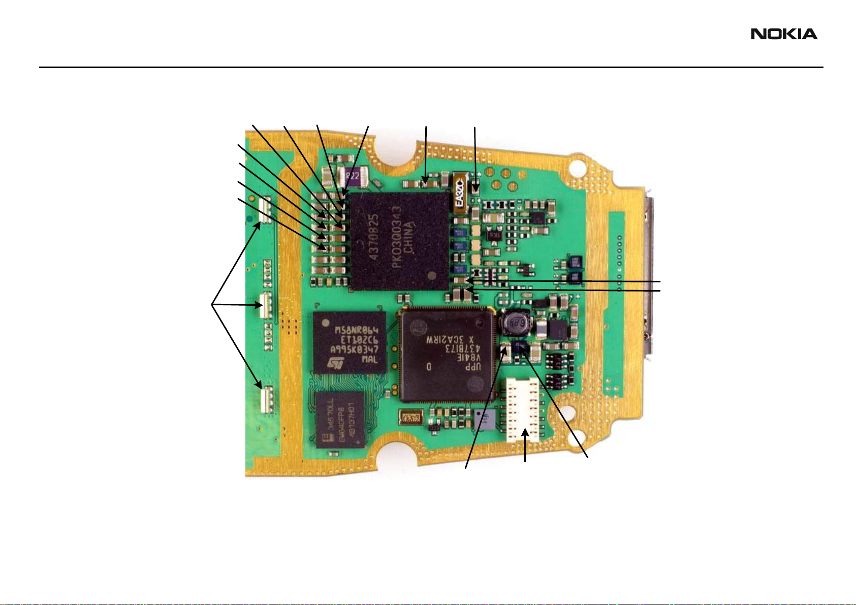
BB Test Points
Following are the top and bottom views of the BB test points, regulators, and BB ASICs.
Page 24 ©2004 Nokia Corporation Company Confidential Issue 1 - Revision 002 09/2004
Page 25

6015/6015i/6016i/6019i (RH-55), 6012 (RM-20)
Nokia Customer Care Troubleshooting - Baseband
Top View
VIBRA
VBAT_VIBRA
VPP
FBUSTXO
FBUSRXO
MBUS
TOMAHAWK
CONNECTOR
POWERONX
19.2 MHz CLK
FBUSRXI
FBUSTXI
UEMSRTX
MBUSTX
GND
BSI
VBAT
DBUS_EN
MBUSRXSMPSCLK
PURX
CBUS_EN
Issue 1 - Revision 002 09/2004 ©2004 Nokia Corporation Company Confidential Page 25
Page 26
6015/6015i/6016i/6019i (RH-55), 6012 (RM-20)
Troubleshooting - Baseband Nokia Customer Care
Bottom View
Display
LED’s
VR2
VR7
VR3
VR5
VR4
VR6
VR1B
FLASH
SRAM
VR1A
VFLASH1
UEM
VANA
VIO
VSIM
UPP
DC-DC
VCORE
KEYPAD
CONVERTER
CONNECTOR
Page 26 ©2004 Nokia Corporation Company Confidential Issue 1 - Revision 002 09/2004
Page 27
6015/6015i/6016i/6019i (RH-55), 6012 (RM-20)
Nokia Customer Care Troubleshooting - Baseband
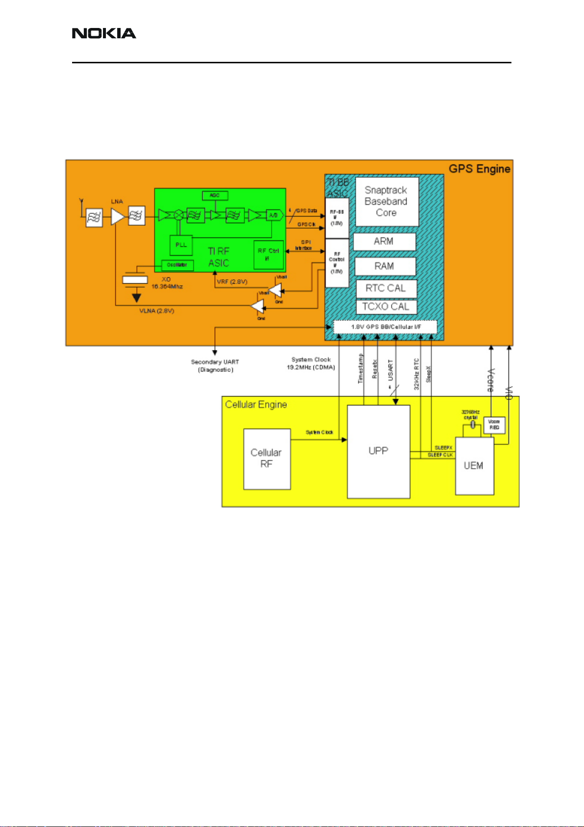
GPS Module (6015i/6016i/6019i)
The GPS circuitry utilizes RF signals from satellites stationed in geosynchronous orbit to
determine longitude and latitude of the handset. The GPS circuitry is completely separate
of the CE circuitry and is located almost exclusively on the secondary side of the PWB
underneath the display module.
Figure 17: GPS block diagram
To troubleshoot the GPS BB:
1. Perform a visual inspection on the GPS circuitry to see if the problem is physical
(dislodged parts, corrosion, poor solder joints, etc.).
2. Put the GE and CE in the proper mode.
3. Check to make sure that necessary inputs from the CE are good (power, clock,
etc.).
4. Ensure that the inputs produce the proper outputs. Because of the large level of
integration (most functionality is contained in the two ASIC chips), the amount
of diagnostics you can perform are limited.
Issue 1 - Revision 002 09/2004 ©2004 Nokia Corporation Company Confidential Page 27
Page 28
6015/6015i/6016i/6019i (RH-55), 6012 (RM-20)
D
Troubleshooting - Baseband Nokia Customer Care
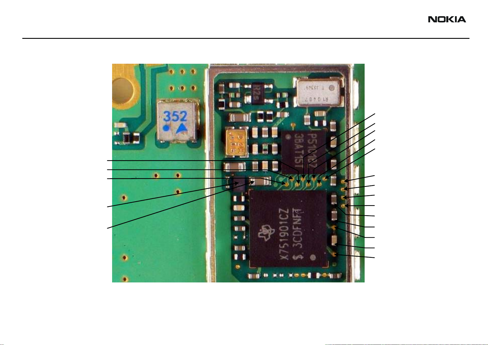
GPS Test Points
GPS_B3
GPS_B2
GPS
RF ASIC
GPS_SPI_CLK
GPS_B1
GPS_B0
GPS_CLK
GPS_SPI_DATA
GPS_SPI_EN
VRF_GPS
REGULATOR
VRF_GPS
Page 28 ©2004 Nokia Corporation Company Confidential Issue 1 - Revision 002 09/2004
GPS BB ASIC
GPS_EN_RESET
GPS_INT_UI_CLK
GPS_UIRX
GPS_UITX
VCORE_GPS
VIO_GPS
GPS_RFCLK
GPS_RFCLK
GPS_INT_DATA_R
Page 29
6015/6015i/6016i/6019i (RH-55), 6012 (RM-20)
Nokia Customer Care Troubleshooting - Baseband
Top Troubleshooting Map
Top
P hone totally dead
NO
Flas h programming
does n't work
NO
P hone doesn't s tart
up or phone is
jammed
NO
YES
YES
YES
Phone
dead
Flash
faults
Phone is
jammed
C harging does n't
work
NO
YES
Top page 2
Charger
faults
Issue 1 - Revision 002 09/2004 ©2004 Nokia Corporation Company Confidential Page 29
Page 30
6015/6015i/6016i/6019i (RH-55), 6012 (RM-20)
Troubleshooting - Baseband Nokia Customer Care
Top 2
Audio faults
NO
Dis play or L E Ds not
working
NO
Keypad doesn't work
YES
YES
YES
Audio
faults
Dis play
faults
Keypad
faults
END
Page 30 ©2004 Nokia Corporation Company Confidential Issue 1 - Revision 002 09/2004
Page 31
6015/6015i/6016i/6019i (RH-55), 6012 (RM-20)
Nokia Customer Care Troubleshooting - Baseband
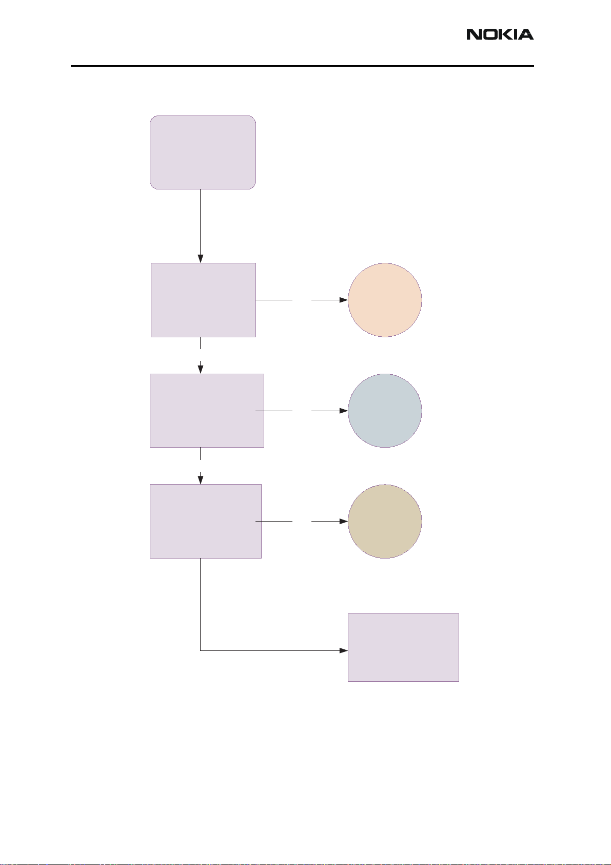
Phone is Totally Dead
Phone is
dead
Phone current is
zero or too high?
NO
YES
¾ If the current is zero, check the battery
connector and make sure the Vbat connector
makes contact.
¾ If current is too high, check for shorts.
¾ Make sure all BB regulators are at their
respective voltage levels (VANA, VIO,
VCORE[DC/DC], VFlash1, and VR3). See
phone's top view diagram for test points.
¾ Make sure the System Clk is 19.2MHz.
¾ Make sure PURX and SleepX signals are high
(1.8V).
Phone current is
<=30 mA
Phone current is
35 mA
YES
Is phone in Local
Mode?
YES NO
YES YES
NO
Is phone flash
programming OK?
NONO
Flash
faults
Check BSI line at the
NO YES
battery connector
and test point. Are
they OK?
Phone is
jammed
Change UEM
RepairOK restart
Issue 1 - Revision 002 09/2004 ©2004 Nokia Corporation Company Confidential Page 31
Page 32

6015/6015i/6016i/6019i (RH-55), 6012 (RM-20)
Troubleshooting - Baseband Nokia Customer Care
Flash Programming Does Not Work
Flash
faults
Phone does not set
Flashbus TXD line
high after startup
NO
Measure BSI pulse
YES NO
during Flash
programming. Is it
OK?
YES
Measure FBusRxO
(2.78V) signal during
flash programming from
production pattern and
FBUSRXI test point
(1.8V). Is it the same?
YES
Measure FBusTxO
(2.78V) during flash
programming from
production pattern and
FBusTXI (1.8V) test
point. Are they the
same?
Check BSI line X100,
C230, R203, R202
NO
Reflow or change
UEM
Change UPP
Is there a pulse on
NO
FBusTXI?
YES
NO
Does the phone set
Flashbus TXD line
low after the line has
been high?
NO
Change UEM
YES
Is there a pulse on
FBusTxO?
NO
Reflow or change
YES
UEM
Measure MBus (2.78V)
YES
Flash
faults,
page 2
from production pattern
and MBusTX and
MBusRX test points. Are
they the same?
NO
Reflow or change
UEM
Page 32 ©2004 Nokia Corporation Company Confidential Issue 1 - Revision 002 09/2004
Page 33

6015/6015i/6016i/6019i (RH-55), 6012 (RM-20)
Nokia Customer Care Troubleshooting - Baseband
Flash
fault s ,
page 2
Can you read
manufacturer ID and
device ID during
flashing?
YES
NO
Reflow or change
flash
Is the manufacturer
ID and device ID
correc t for th a t p art?
YES
Is phone totally
dead?
NO
Phone doesn't start
up or phone is
jammed?
NO
NO
YES
YES
Reflow or change
UPP
Phone is
dead
Phone is
jammed
Retest
Issue 1 - Revision 002 09/2004 ©2004 Nokia Corporation Company Confidential Page 33
Page 34

6015/6015i/6016i/6019i (RH-55), 6012 (RM-20)
Troubleshooting - Baseband Nokia Customer Care
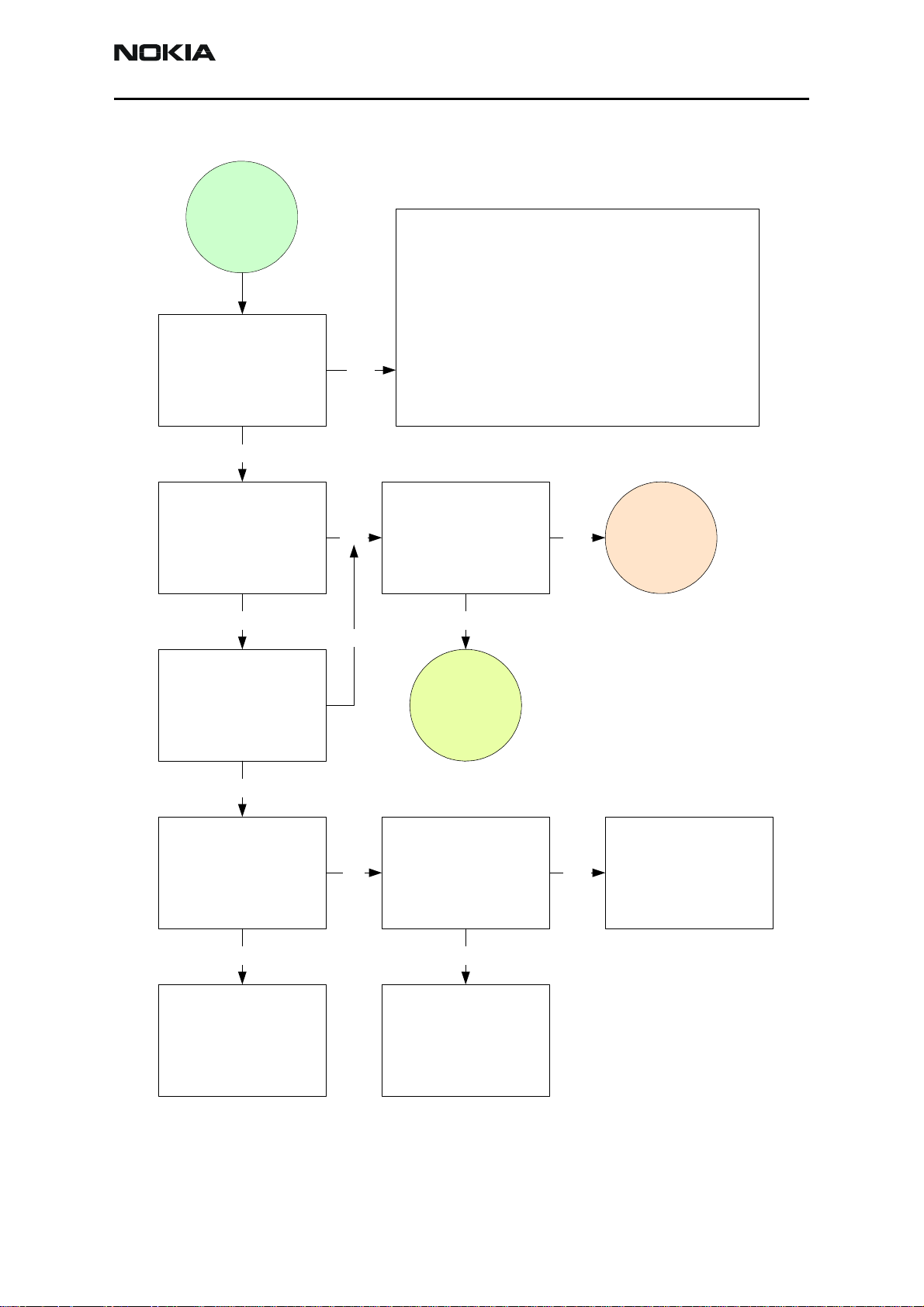
Phone is Jammed
Phone is
jam med
Check VBATT, VIO,
VCORE, VFlash1,
VANA, VR3
Measure VIO,
VCORE, VFlash1,
VANA, and VR3
voltages. Are they
OK?
YES
NO
capacitors. Are they
OK? (See phone top
view diagram for
capacitor locations)
YES
NO
Repair
Check BSI/BTEMP
lines and VBATT
line s . If OK, reflow
or change UEM.
Measure 19.2MHz RF
Clk a t C068 . Is it
OK?
YES
Measure PURX and
SleepX at test
points. Are they high
(1.8V ) ?
YES
Phone is
jam med,
page 2
Measure 19.2MHz
NO NO
Clk coming from
VCTCXO at C523
and R517. Is it O K?
YES
NO
Change UEM
Check G501. If not
OK, change G501.
Change UPP
Page 34 ©2004 Nokia Corporation Company Confidential Issue 1 - Revision 002 09/2004
Page 35

6015/6015i/6016i/6019i (RH-55), 6012 (RM-20)
Nokia Customer Care Troubleshooting - Baseband
Phone is
jam m e d ,
page 2
Phone shutdown
after 32 seconds
NO
Measure
DB usClk 9.6 M Hz
and Dbus
interface signals
at test points.
Are they OK?
YES
Read phone info.
Is it O K ?
YES
YES
Can ESN be read
from the phone?
YES
Measure
watchdog signal
at Cbu s in te rf ac e
NO
at test points.
Are they OK?
YES
NO
Reflow or
change UPP
Measure
FBusRxO signal
NO NO
during phone
info r ea d fro m
tes t p o in t . Is it
OK?
YES
Measure
FBusTxO signal
during phone
info r ea d fro m
tes t p o in t . Is it
OK?
YES
NO
the security
change UPP and
change UEM and
change UEM
Rebuild E SN at
NO
change UPP
station.
Reflow or
reflash
Reflow or
reflash
Reflow or
Reflow or
Retest
Reflow or
change UEM
Issue 1 - Revision 002 09/2004 ©2004 Nokia Corporation Company Confidential Page 35
Page 36

6015/6015i/6016i/6019i (RH-55), 6012 (RM-20)
Troubleshooting - Baseband Nokia Customer Care
Charger Faults
Charger
faults
Connect
charger. Make
sure battery is
connected.
Battery bar
doesn't work
(scroll)
NO
Retest
YES
Measure voltage
over V100. Is it >
3.0 Vdc?
YES
Read BTEMP
value. Is it ~25C
(0319)?
YES
Remove (fuse)
F100 and
measure current.
Is it ~350 -
390mA?
YES
NO
NO
NO
Check X102,
F100, L100,
V100, C102.
Check NTC
YES
Change UEM
NO
Replace NTC
Retest
Page 36 ©2004 Nokia Corporation Company Confidential Issue 1 - Revision 002 09/2004
Page 37

6015/6015i/6016i/6019i (RH-55), 6012 (RM-20)
Nokia Customer Care Troubleshooting - Baseband
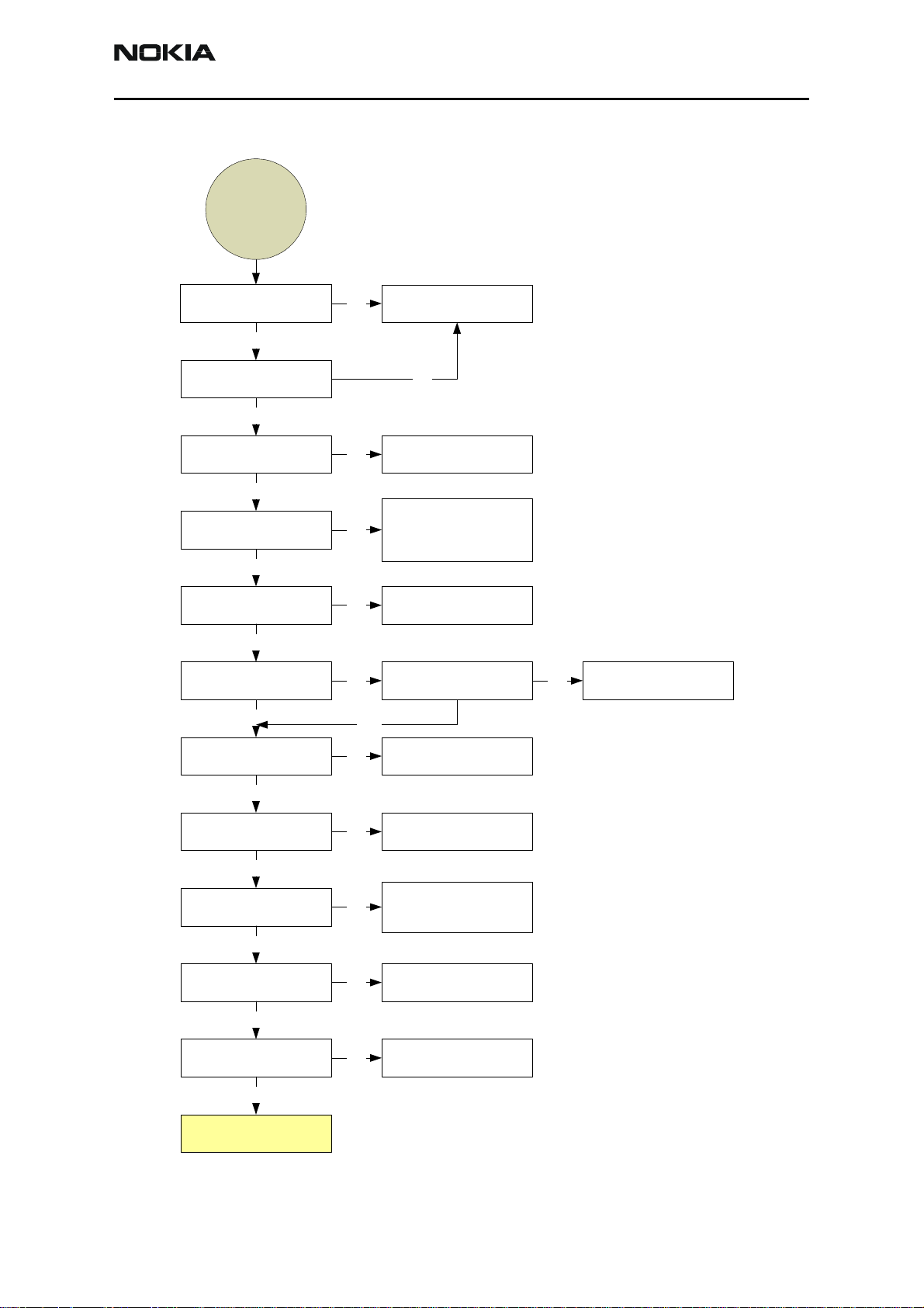
Audio Faults
Earpiece
Audio
faults
Is the earpiece
working?
YES
Change
NO YES
Set phone in Local Mode. Use
Phoenix Troubleshooting >
Phone Control > Phone State
tab > Select Local Mode > click
Execute. Then use Autio Test >
HP microphone in/HP speaker
earpiece. Inject a 1KHz sine
earpiece. Is it
working now?
NO
out > Loop ON to enable
signal 200Vp-p on XMIC.
Is the signal
coming out of
the UEM on
EARP and
EARN?
NO
Retest
Check UEM. If
not OK, change
the UEM.
YES
Check R150. If
OK then change
the earpiece.
Audio
faults,
page 2
Issue 1 - Revision 002 09/2004 ©2004 Nokia Corporation Company Confidential Page 37
Page 38

6015/6015i/6016i/6019i (RH-55), 6012 (RM-20)
Troubleshooting - Baseband Nokia Customer Care
Microphone
Audio
faults,
page 2
Is the
microphone
working?
YES
Change the
NO YES
microphone. Is it
working now?
NO
Set phone in Local Mode. Use
Phoenix Troubleshooting >
Phone Control > Aphone State
Tab > select Local Mode > click
Execute. Then use Audio test >
HP microphone in/HP speaker
out > Loop ON to enable the
earpiece. Talk through the
microphone.
Measure MICB1
voltage from MICP
pads on bottom
NO
connector.
Is it ~2.1V?
Retest
Check C170, C172,
and C151. If OK,
change UEM.
YES
Is the signal going
to the UEM at MIC1P
and MIC1N at C150?
YES
Is the signal going
out of the UEM at
XEARP, pin 12 on
the bottom
connector?
YES
NO
NO
Check audio
ASIPs Z150, Z151,
R150, then change
the microphone.
Check R160, R162,
R153, and R163. If
OK, change the
UEM.
Audio
faults,
page 3
Retest
Page 38 ©2004 Nokia Corporation Company Confidential Issue 1 - Revision 002 09/2004
Page 39

6015/6015i/6016i/6019i (RH-55), 6012 (RM-20)
Nokia Customer Care Troubleshooting - Baseband
IHF
Audio
faults,
page 3
Check IHF audio
NO NO
Is IHF working?
YES
Set the phone to Local Mode. Use
Phoenix to open Troubleshooting >
Phone Control > Phone State tab >
select Local Mode > click Execute.
microphone in/ Ext speaker out >
Loop ON. To enable IHF, turn on
GenIO(10). Measure an d c h ec k IHF
test points J150 and J151. Is it OK?
amplifier (N150).
Is it OK?
YES
Then use Audio test > HP
Replace N150.
GenIO(10). If not
NO
OK, change the
Check
UEM.
Audio
faults,
page 4
YES
Change IHF speaker.
Issue 1 - Revision 002 09/2004 ©2004 Nokia Corporation Company Confidential Page 39
Page 40

6015/6015i/6016i/6019i (RH-55), 6012 (RM-20)
Troubleshooting - Baseband Nokia Customer Care
Vibra
Audio
faults,
page 4
Is Vibra
working?
YES
Measure VBATT
NO NO
voltage pin 1 of
M300. Is it OK?
YES
Use the UI Menu > Profile >
Normal > Customize >
Vibrating Alert > Select On >
then go back to Customize
Menu > Ringing Tone > Try
any ring tone. Does the
vibra work?
YES
Measure the
UEM signal on
pin 2 of M300. Is
NO
the signal OK?
YES
Check VBATT
line
Change the UEM
Change Vibra
END
Page 40 ©2004 Nokia Corporation Company Confidential Issue 1 - Revision 002 09/2004
Page 41

6015/6015i/6016i/6019i (RH-55), 6012 (RM-20)
Nokia Customer Care Troubleshooting - Baseband
Display Faults
Display
faults
Are the UI module
and display LEDs
turned on when the
phone is turned on
or when making a
call?
Measure KLIGHT at
NO NO
J300, Vbat at C312,
and Pout at C313.
Are they OK?
YES
Measure R300, R301,
(~6.3). Check V300
NO
and V301.
If Vbat is not OK,
check the battery. If
Pout is not OK,
check N300.
Replace
YES
Display
faults,
page 2
YES
Check X300 and
Z300.
YES
Measure the
KLIGHT.
Is the signal OK?
YES
Check N300.
Measure R300 and
R301 should be 1.5
X Vbat. Is it OK?
YES
Change LEDs
NO
NO
NO
Replace
Change UEM
Change N300
Issue 1 - Revision 002 09/2004 ©2004 Nokia Corporation Company Confidential Page 41
Page 42
6015/6015i/6016i/6019i (RH-55), 6012 (RM-20)
Troubleshooting - Baseband Nokia Customer Care
Display
faults,
page 2
Does the Display
show an image?
YES
Try changing
NO YES
display module.
Is it OK?
NO
Measure VIO and
VFLASH1. Is it
NO
OK?
Check LCD signals
LCDCSX (pin2), LCDCLK
(pin5), LCDDA (pin4),
and XRES (pin1). Are the
signals OK? (Refer to
the display section.)
YES
Retest
Change UEM
NO
Change UPP
Change Display
END
Page 42 ©2004 Nokia Corporation Company Confidential Issue 1 - Revision 002 09/2004
Page 43

6015/6015i/6016i/6019i (RH-55), 6012 (RM-20)
Nokia Customer Care Troubleshooting - Baseband
Keypad Faults
Power Key
Keypad
faults
Is the power key
working?
YES
Keypad
faults,
page 2
Measure voltage
NO NO
at pin 1 and 3
(S300). Is it
high?
YES
Measure voltage
at pin 1 and 3
(S300) when the
power key is
YES
pressed. Is it
high?
NO
Phone is
Jammed
C314, and R304.
If OK, change
Check S300. Is it
OK?
NO
Change S300
Check S300,
UEM
YES
Phone dead
Issue 1 - Revision 002 09/2004 ©2004 Nokia Corporation Company Confidential Page 43
Page 44

6015/6015i/6016i/6019i (RH-55), 6012 (RM-20)
Troubleshooting - Baseband Nokia Customer Care
UI Modules
Keypad
faults,
page 2
Are UI modules
keys working?
YES
Change keypads
NO
module. Is it
working?
Measure ROW0-4
Keyb(5) and
Keyb(9) signasl
between UPP and
Z300. Are they
~1.8V?
Measure ROW0-4
Keyb(5) and
Keyb(9) signals
between Z300 and
X300. Are they
~1.8V?
NO
YES
YES
YES
NO
NO
Retest
Make sure there
are no shorts on
Z300. If OK,
change the UPP.
Change Z300
Make sure there
END
are no shorts on
Z300. If OK,
change UPP
Page 44 ©2004 Nokia Corporation Company Confidential Issue 1 - Revision 002 09/2004
Page 45
6015/6015i/6016i/6019i (RH-55), 6012 (RM-20)
Nokia Customer Care Troubleshooting - Baseband
GPS
GPS faults
Is VCORE at 1.5V?
YES
Is VIO at 1.8V?
YES
GPS_RF_CLK
(19.2MHz) OK?
YES
GPS_EN_RESET held
high?
YES
GPS_SLEEPCLK
(32.768KHz) OK?
YES
VRF_GPS OK?
YES
GPS_CLK (16.368MHz)
OK?
NO
NO
Troubleshoot CE
power supply
NO
Troubleshoot CE
VCTCXO circuit
If the BB ASIC is being
NO
held in reset,
troubleshoot the
source in the CE
Troubleshoot CE sleep
NO
NO
YES
NO
clock circuit
VRF_GPS regulator
enable line low?
Replace TCXO or GPS
RF ASIC
NO
Replace regulator
N052
YES
Test Mode 1 OK?
YES
CE sending code
download signals?
YES
SPI interface active?
YES
RF data and clock?
YES
Debug RF front end
NO
Replace GPS BB ASIC
Determine why CE not
NO
NO
NO
sending download
Replace GPS BB ASIC
Replace GPS RF ASIC
signals
Issue 1 - Revision 002 09/2004 ©2004 Nokia Corporation Company Confidential Page 45
Page 46

6015/6015i/6016i/6019i (RH-55), 6012 (RM-20)
Troubleshooting - Baseband Nokia Customer Care
This page intentionally left blank.
Page 46 ©2004 Nokia Corporation Company Confidential Issue 1 - Revision 002 09/2004
 Loading...