

Page 1
CONFIDENTIAL
Service & Analysis Center Europe
Training Team
Version 1.0 / 19.10.1999 Page 1 of 38
Page 2

CONFIDENTIAL
Service & Analysis Center Europe
Change history
Orginator Approved Status Version Date Comment
Ralf Heptner Draft 0.1 11.08.99
Ralf Heptner Draft 0.2 25.08.99 Flowcharts updated
Ralf Heptner Draft 0.3 27.09.99 SIM lock lists updated, some
minor changes
Ralf Heptner Draft 0.4 01.10.99 Forword changed
Jose Marquez Draft 0.5 08.10.99 Forword changed
Ralf Heptner Approved 1.0 19.10.99 Forword changed
Training Team
Version 1.0 / 19.10.1999 Page 2 of 38
Page 3

CONFIDENTIAL
Service & Analysis Center Europe
Training Team
Introduction
IMPORTANT:
This document is intended for use by authorized NOKIA service centers only.
The purpose of this document is to provide some further service information for
NOKIA 6110, 5110 phones.
It contains a lot of collected tips and hints, to find failures and repair solutions easily.
I will also give support to the inexperienced technicians.
Saving processe time and improving the repair quality is the aim of using this document.
We have build it up based on fault symptoms (listed in "Contents") followed by detailed description for further
analysis.
It is to be used additionally to the service manual and other service information
like Service Bulletins, for that reason it doesn't contain any circuit descriptions or schematics.
All measurements are made with using of following equipment:
Nokia repair SW : Wintesla Version 6.10
DLL version : NSEKM-13 version 2.41.03
Nokia Module Jig : JBS-19
Digital multimeter : Fluke 73
Oscilloscope : Hitachi V-1565; Fluke PM 3380A
Spectrum Analyzer : Advantest R3361C with an analogue probe
RF-Generator / : Rohde & Schwarz CMD 53
GSM Tester
While every endeavour has been made to ensure the accuracy of this document, some errors may exist. If any
errors are found by the reader, NOKIA should be notified in writing, using following procedure:
Please state:
Title of the Document + Issue Number/Date of publication
Page(s) and/or Figure(s) in error
Please send to:
Version 1.0 / 19.10.1999 Page 3 of 38
Nokia GmbH
Service & Analysis Center Europe
Meesmannstr.103
D-44807 Bochum / Germany
Email: ams.sace-training@nokia.com
Page 4

CONFIDENTIAL
Service & Analysis Center Europe
Training Team
Contents
CHANGE HISTORY .............................................................................................................................................. 2
INTRODUCTION ................................................................................................................................................... 3
P
HONE DOESN'T SWITCH ON
P
HONE SWITCHES ITSELF OFF
S
WITCH ITSELF OFF- CONTACT SERVICE APPEARS ON THE DISPLAY
C
ONTACT SERVICE
C
ONTACT SERVICE
C
ONTACT SERVICE
C
ONTACT SERVICE
C
LOCK TIME OR USER SETTING PROBLEMS
T
HE PHONE HANGS UP, AFTER ENTERING THE
N
OT CHARGING
L
OW STAND BY TIME
B
UZZER FAILURES
I
NTERNAL AUDIO FAILURES
E
XTERNAL AUDIO FAILURES
A
CCESSORY DETECTION FAILURE (HEADSET / CAR KIT ACTIVE
D
ISPLAY FAILURE
K
EYPAD FAILURE
NSERT
I
SIM
L
OW RECEIVER SIGNAL STRENGTH INDICATOR
N
N
N
N
N
C
ALL BREAKS
N
N
SIM
CARD NOT ACCEPTED
O SERVICE
RX (
O
NO RX CALIBRATION
RX (
O
NO RX CALIBRATION
RX (
O
NO RX CALIBRATION
RX (
O
NO RX CALIBRATION
O CALL / SERVICE
O OR TO LOW
– COBBA
– COBBA
– E
– PPM
....................................................................................................................................................17
.................................................................................................................................................22
..................................................................................................................................................27
...................................................................................................................................................29
CARD
.........................................................................................................................................................35
/ N
O SERVICE
O.K........................................................................................................................................38
TX – P
....................................................................................................................................5
...................................................................................................................................8
PARALLEL BUS FAILED
SERIAL BUS FAILED
EPROM TUNE CHECKSUM FAIL
VALIDITY
.......................................................................................................................13
.................................................................................................10
.....................................................................................................11
................................................................................................12
...............................................................................................................14
PIN-
...........................................................................................16
CODE
............................................................................................................................................21
....................................................................................................................................23
...................................................................................................................................24
)....................................................................................25
...........................................................................................................................................30
, SIM LOCK
FAILURE
......................................................................................................31
...........................................................................................................35
…RSSI
…RSSI
…RSSI
…RSSI
READING FIXED VALUE
READING HIGH DIFFERENCE
READING HIGHEST VALUE
READING HIGHEST VALUE
).....................................................................................36
...................................................................................................................................38
................................................................................................................................38
OWER
...............................................................................9
)..............................................................................36
).................................................................................36
).................................................................................37
Version 1.0 / 19.10.1999 Page 4 of
38
Page 5

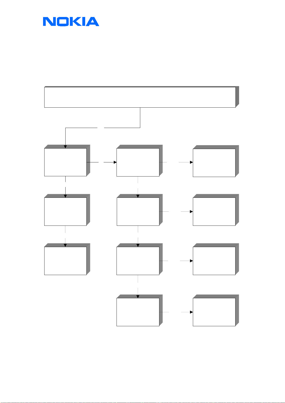
Phone doesn't switch on
Figure 1: Flow chart of phone doesn't switch on
Phone doesn't switch on
CONFIDENTIAL
Service & Analysis Center Europe
Training Team
Observe power consumtion
norm. < 6mA pulsing to
20mA
(without backlights)
Yes
Check VBAT (3,6V)
N100 / 8, 12, ...
Yes
Check 32,768 KHz
N100 / 46 = 1,3Vss (Sinus)
N100 / 47 = 2,3Vss
(Square)
Yes
Check DC Volt. PW RONX
N100 / 29 = V BATT (3,6V)
If Pwr but ton is pressed
PWRONX = 2,9V
Yes
Check DC Volt. PURX
N100 / 54 = 2,8V
D200 / 122 = 2;8V
(after pressing Pwr button!)
Yes
Check Sleep clk 32,768KH z
N100 / 48 = 2,8Vss
D200 / 122 = 2,8Vss
(Square)
Yes
Check DC Volt SLEEPX
D200 / 113 = 2,8V
N100 / 24 =2,8V
Yes
Check
No No
No
No
No
No
No
No
C610, C 611,
C612
if faulty!
Check connection
to X101
L103
Change
B100
Check:
R118 (10K)
X300
UI-module
Chec k solderings
of N100
or
Change N100
Chec k solderings
of N100
or
Change N100
Chec k solderings
of D200
or
Change D200
Lift L550
(VBATT for Pwr
Amp)
No
Change
N550
Check DC Volt VXO
N100 / 25 = 2,8V
G600 / 1 = 2, 8V
Yes
Check VCXO 13MHz
G600 / 2 = 1Vss
D200 / 93 = 1V ss
Yes
Try to flash
the phone
No
No
No
Chec k solderings
of N100
or
Change N100
Change
G600
See Section:
Can't Flash the
phone
Version 1.0 / 19.10.1999 Page 5 of
38
Page 6

CONFIDENTIAL
N100 faulty/ poor solderings
Check if voltage on Pin 29 drops of 700 mV during pressing the Power on button
•
Check if there is a 32.768 KHz square wave on Pin 48
•
Check if PURX Pin 54 goes up to 2.8 V DC
•
Check if VXO Pin 28 goes up to 2.8 V DC
•
B100 faulty 32,768KHz
Check 32.768 KHz ; 1 Vpp clock signal on B100
•
G600 faulty 13 MHz
Check VXO 2,8V DC on J522
•
Check 13 MHz; 1 Vpp on output
•
S001 User Interface
Check if voltage on Pin 29 drops of 700 mV during pressing the Power on button
•
Service & Analysis Center Europe
Training Team
X300 UI Connector bent
Check if voltage on Pin 29 drops of 700 mV during pressing the Power on button
•
R118 missing/ poor soldering
Check if voltage on Pin 29 drops of 700 mV during pressing the Power on button
•
D200 MAD faulty/ poor soldering
Check 32.768 kHz square wave on Pin 124 (comes from CCONT Pin 48)
•
Check 13 MHz 0n Pin 93 (comes from G600)
•
Check VBB 2.8 V DC
•
Check PURX 2.8 V DC on Pin 122 (comes from CCONT Pin 54)
•
Check SLEEPX 2.8 V DC 0n Pin 113
•
Resolder MAD complete
•
D210 FLASH faulty/ poor soldering/ empty
Check VBB 2.8 V DC on Pin 47
•
If power consumption is around 20mA try to flash the phone
•
Resolder FLASH completely
•
Version 1.0 / 19.10.1999 Page 6 of
38
Page 7

CONFIDENTIAL
L103 faulty/ poor soldering
Check VB on J232
•
X101 / X102 contacts bent/ dirty
Check if VBATT and Gnd are connected
•
N550 short circuit
If there is a short circuit on VBATT, lift L550 and check again
•
If the PCB is burnt, swap the phone
•
C610; C611; C612 burnt/ short circuit
Lift the capacitor and check again
•
If the PCB is burnt, scrap the phone
•
Service & Analysis Center Europe
Training Team
Figure 2: Block diagram of switching on routine
VBATT
R103 / R104
VCHAR
BTEMP
SLEEPX
VCXO
13 MHz
G600
C213
R213
93
12, 16, ...
60
63
25 VXO 2.8V
24
113
2.8V
BB Regulator VBB 2.8V
55
CCONT
N100
54
48
124
32 KHz
square
122
2.8V
GENSIO
MAD2
D200
46
47
29
PURX
B100
32 KHz
Crystal
R118
Pwr OnX
from
UI module
Version 1.0 / 19.10.1999 Page 7 of
38
Page 8
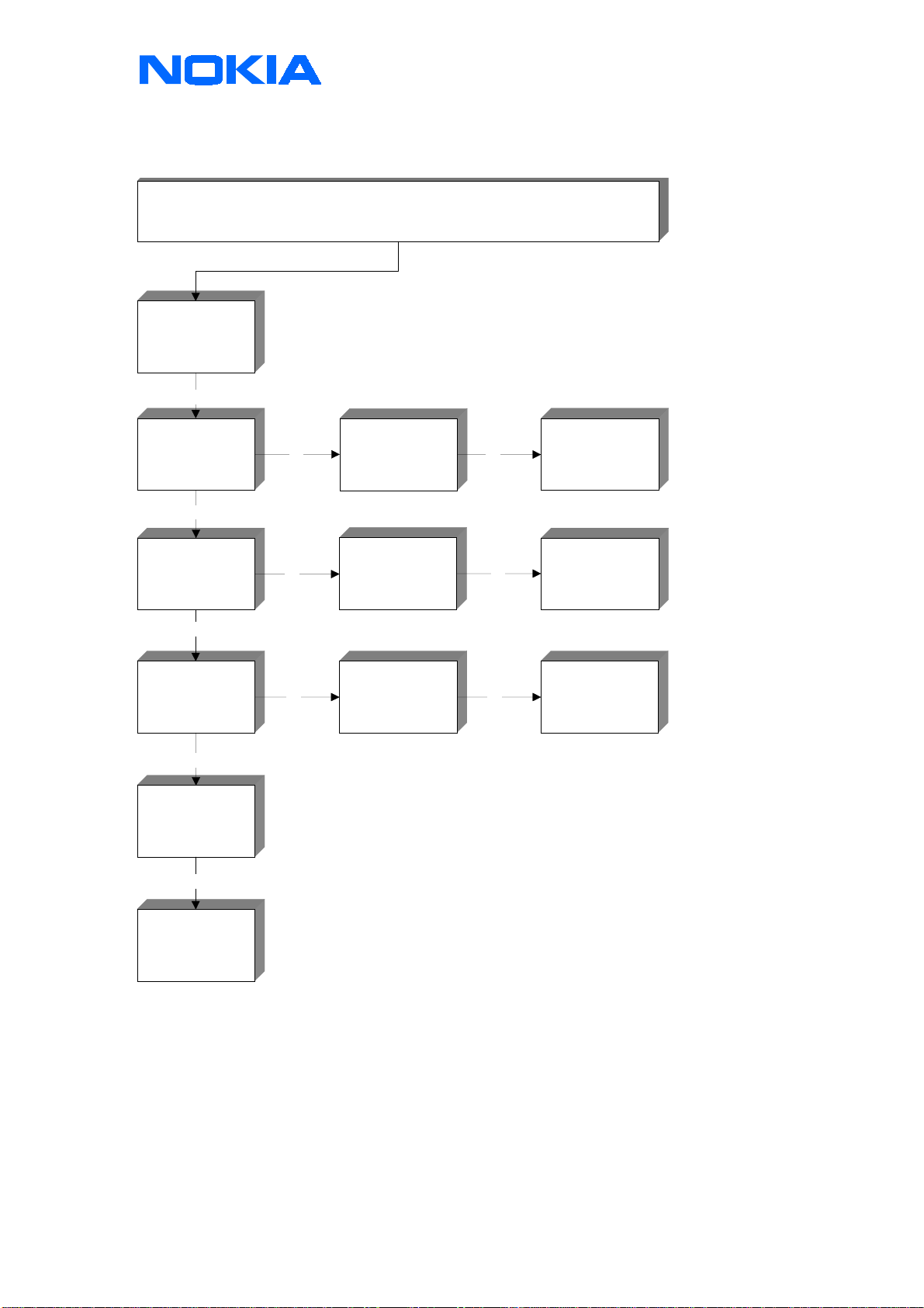
Phone switches itself off
Yes
CONFIDENTIAL
Phone intermittend switches off
Service & Analysis Center Europe
Training Team
Check if this happens
only with 5V SIM-cards
and if the phone work s
probably with 3V SIM's
Yes
Check the 5V
supply voltage on
C131 wit h an
oscilloscope
Yes
Change C131 if the
noise is higher than
350mVpp
Check X101 and
No Wrong
X102, if poor soldered,
bent or soiled
Change if old version
is used!
No
Check amplitude of
32,768KHz square
wave at pin 124 of
MAD (2,8Vpp)
No
Check amplitude of
13MHz at pi n 93 of
MAD (2,8Vpp)
No
Wrong
Wrong
Resolder, change or
clean the connector
Change or check
soldering of B100,
N100, R154, C101,
C102
Change or check
soldering of G600,
V705...
Check VBB 2,8V DC
on pin 55 of N100
Wrong
Change or check
soldering of N100,
C107
Version 1.0 / 19.10.1999 Page 8 of
38
Page 9

CONFIDENTIAL
C131 10μF/10V
Check that the handset work probably with 3V SIM-cards
•
Check the 5V supply voltage at C131 (about 4,8V-5,2V,
•
Maximum noise 350mVpp overlap)
Figure 3: diagram of normal noise on C131
Service & Analysis Center Europe
Training Team
Switch itself off- contact service appears on the display
D200 MAD faulty / poor soldering
Check the amplitude of the 32,768KHz square wave on pin 124 (comes from CCONT pin 48)
•
Check the amplitude of the 13MHz clock frequency pin 93 (from G600)
•
Check VBB 2,8V DC
•
Resolder MAD
•
Internal error of MAD
•
Version 1.0 / 19.10.1999 Page 9 of
38
Page 10
CONFIDENTIAL
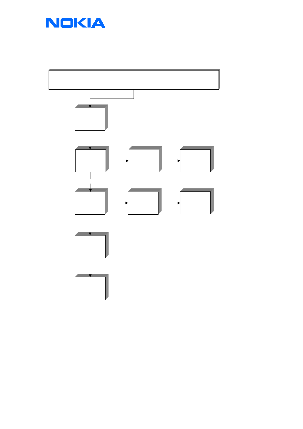
Contact service – COBBA parallel bus failed
Contact Service
Check via WINTESLA / Testing / Selftest
which kind of selft est is fail
COBBA parallel bus
failed
Yes
Service & Analysis Center Europe
Training Team
check COBBACLK
13MHZ/ 3,2Vpp on pin
45 0f COBBA
Ok
check VBB 2,8V on
pin 27, 53 of COBBA
Ok
Check VCOBBA 2,8V
DC on pin 7, 12, 21,
25 of COBBA
Ok
Check so lder ing of
MAD or change MAD
Ok
No
No
No No
Check COBBA Clk on
pin 144 of MAD
Check VBB 2,8V DC
on pin 55 of N100,
CCONT
Check VCOBBA 2,8V
DC on pin 22 of N1 00,
CCONT
No
No
Change or check
soldering of MAD
check soldering or
change N100, C107
Change or check
soldering of N100,
C133
Check so lder ing of
COBBA or change
COBBA
Version 1.0 / 19.10.1999 Page 10 of
38
Page 11
CONFIDENTIAL
Contact service – COBBA serial bus failed
Contact Service
Check via WINTESLA / Testing / Selftest
which kind of selftest is faulty
COBBA Serial
bus failed
Yes
Service & Analysis Center Europe
Training Team
Check VBB 2,8V
DC on pin 27, 53
of COBBA
Ok
Check VCOBBA
2,8V DC on pin 7,
12, 21, 25 of
COBBA
Ok
Check soldering
of COBBA or
change COB BA
Ok
Check soldering
of MAD or change
MAD
No
No
Check VBB 2,8V
DC on pin 55 of
N100, CCONT
Check VCOBBA
2,8V DC on pin
22 of N100
No
No
Change or check
soldering of
N100, C107
Change or check
sol dering of
N100, C133
N250 COBBA faulty / poor soldering
Check VBB 2,8V DC on pin 27, 53 from COBBA
•
Check VCOBBA 2,8V DC on pin 7,12,21,25, from COBBA
•
Check COBBACKL 13MHz 3,2Vpp pin 45 from COBBA
•
Resolder COBBA
•
Internal error of COBBA
•
Note! Rewrite SIMLOCK and IMEI entries with use of the Nokia security SW (SSSW) and make a SW-update or send this
phones to the SACE, if this procedure is not permitted to you
Version 1.0 / 19.10.1999 Page 11 of
38
Page 12

CONFIDENTIAL
Contact service – Eeprom tune checksum fail
Contact Service
Check via WINTESLA / Testing / Selft est
which kind of selftest is faulty
EEPROM tune
checksum f ail
Yes
Service & Analysis Center Europe
Training Team
Check via WINTESLA >
product i nf or mation, i f
any phon e data, like:
IM EI, product code,
PSN, etc. is corrupted
change the EEPROM if
it is permitted to y ou, to
rewrite the IMEI
Reset t he phone (don't
No
Yes No
use the full fact or y set if
it is not permitted to you
to rewrite the IMEI)
EEPROM
internal fault
send this phones to the
SACE Bochum
if it is not permitted to
you to r ewrit e t he IMEI
refer to
Service Bulletin
general 26
Phone is Ok, if
CONTACT SERVICE
dissapears
D240 Eeprom faulty
Check via wintesla if IMEI or product data are corrupted
•
Don’t use the "Full factory set" via wintesla, otherwise the IMEI will
•
Change to question marks
Change the Eeprom if it's permitted for you and write all ID data (IMEI, product code…) back
•
If you aren't allowed to change the Eeprom and the IMEI is missing, write a note with a little
•
Comment, and send it together with the phone to the SACE
Note! Rewrite SIMLOCK and IMEI entries with use of the Nokia security SW (SSSW) and make a SW-update or send this
phones to the SACE, if this procedure is not permitted to you
Version 1.0 / 19.10.1999 Page 12 of
38
Page 13

Contact service – PPM validity
Contact Service
Check via WINTESL A / Tes ting / S elfte st
whic h kind of selftest is faulty
CONFIDENTIAL
PPM validity fail
Yes
try to flash the phone
oK
Service & Analysis Center Europe
Training Team
phone is Ok, if
CONTACT
SERVICE dissapears
after flashing
not oK
check soldering or
change D200,
FLASH
SW / D210 Flash faulty / poor soldering
Check if the fault disappear after update the handset
•
Resolder D210 Flash
•
Internal error of Flash
•
Version 1.0 / 19.10.1999 Page 13 of
38
Page 14

CONFIDENTIAL
Clock time or user setting problems
Clock time problems / wrong ringingtone speed
check 32,768KHz
clock frequency on
pin 48 of N100,
CCONT
Check soldering or
change B100, R 154 ,
C101, C102, N100
Clock time / ringing tone is to fast or to slowly
Check that the sleepclk is 32.768KHz square wave on pin 48 CCONT
•
Check the crystal B100, R154, C101, C102, N100
•
Service & Analysis Center Europe
Training Team
Loose of clock time after removal of battery
Backupbattery
keeps the clock
running for min.
10 minutes
No
Check the DC
voltage 2,8V -
3,3V on G100,
backupbattery
No
Check the
springcontacts if
they are bent or
soiled
No
Change G100,
backupbattery
Yes
correct or clean
the contacts
G100, Loose of clock time, if the battery is empty or removed for few minutes
G100 Back up battery faulty / disconnected
•
Check the voltage 2,8V-3,3V over the back up battery connected to the PCB in the service modus
•
Check the spring contacts
•
Clean the back up battery contacts on the board
•
Version 1.0 / 19.10.1999 Page 14 of
38
Page 15

CONFIDENTIAL
Clock freeze after switching on the phone
Yes
Service & Analysis Center Europe
Training Team
Check the
CCONTINT
impulse on pin
52 of N100,
CCONT
Ok
Check the
CCONTINT
impulse on pin
123 of D200,
MAD
No
No
resolder
CCONT or
change if
solderings are
Ok
resolder MAD
or change if
solderings are
Ok
N100, Clock will freeze after switching on
CCONTINT short circuit / break
•
Check the CCONTINT impulse on pin 52 CCONT or pin 123 MAD (see the diagram below)
•
Check pin 52 CCONT pin 123 MAD short circuit or break
•
Figure 4: CCONT INT imp uls e on CCONT pin 52
Version 1.0 / 19.10.1999 Page 15 of
38
Page 16

CONFIDENTIAL
The phone hangs up, after entering the PIN-code
Phone SW hangs up after entering the PIN code
Yes
Service & Analysis Center Europe
Training Team
check the
amplitude of the
32,768 KHz clock /
2,8Vpp on pin 124
of D200, MAD
Ok
check the
amplitude of the
13MHz c loc k on
pin 93 of D200,
MAD
Ok
check VBB 2,8V
DC on pin 59 of
N100, CCONT
Ok
check solder of
MAD or
change if
neccessary
resolder CCONT
No
No
No No
or change if
solderings are Ok.
check G600,
change if
neccessary
check C140,
change if
neccessary
check solder of
CCONT or
change if
neccessary
D200 MAD faulty / poor soldering
Check the amplitude of the 32,768KHz square wave on pin 124 (comes from CCONT pin 48)
•
Check the amplitude of the 13MHz clock frequency pin 93 (from G600)
•
Check VBB 2,8V DC
•
Resolder MAD
•
Internal error of MAD
•
Version 1.0 / 19.10.1999 Page 16 of
38
Page 17

Not charging
CONFIDENTIAL
Service & Analysis Center Europe
Training Team
no confirmation / error message / beep is coming from phone, if charger is
check VCH on pin 1,
16 of N101, CHAPS
Ok
check solderings of
N101 or change if
necessary
pluged in
Check X100, F101,
No Ok
L104, L105 if
connection to charger
is open
Phone doesn't stop charging
Not charging (1)
check V100, C103 if
VCH is short circuited
Do the battery
management
calibrati on
check the power
consumtion of the
phone (1-5mA if
phone is swi tched on
without SIM & lights)
No
check DC voltage on
pin 2 of D200, MAD,
switches from 2,8V to
0V, if battery is fully
charged
Ok
section not charging
No
consumtion is higher,
Ok
No
refer to section low
resolder or change
if any A/D value is
wrong, refer to
(2)
If th e power
standby ti me
MAD if necessary
Yes
Yes
not charging (2)
low standby ti me
Version 1.0 / 19.10.1999 Page 17 of
38
Page 18

CONFIDENTIAL
Service & Analysis Center Europe
Training Team
failed
Charger voltage failed
Battery size
failed
error message ("not charging") / beep is coming fr om phone, if charger is pluged in
Not charging (2)
check DC voltage on pin
Do the battery
management calibration
check DC voltage on pin
Yes
60 of N100/ CCONT
if charger i s pluged in
nominal VCH 1:10 (0,8V)
No
check F101, L104, V100,
C103 and voltage
devider R103, R104
check DC Voltage on pin
Yes Ok
62 of N100, CCONT
9 of N101, CHAPS if
Ok
charger is pluged in
resolder or change D200
resolder or change N100
Ok
Ok
try the calibrating again
resolder or change N100
(2,8V)
No
if necessary
if necessary
if necessary
Try charging, i f no A/D
Ok
valiue was wrong
Battery temperature
failed
Charge current
failed
check battery, X101,
voltage devider R120,
check DC voltage on pin
Yes
Yes
63 of N100, CCONT
check battery, X102,
voltage devider R120,
check DC voltage on pin
No
try the calibrating again
R122
No
R122
2 of N100, CCONT
No
check N101, R131 try the calibrating again
Ok
resolder or change N100
Ok
try the calibrating again
Ok
resolder or change N100
Ok
Ok
if necessary
if necessary
Version 1.0 / 19.10.1999 Page 18 of
38
Page 19

F101 faulty
Check resistance of F101 (0Ω)
•
V100 faulty
Check resistance of V100 (50KΩ in circuit)
•
L104 faulty Vcharge
Check resistance of L104 (0Ω)
•
L105 faulty Charge ground
Check resistance of L105 (0Ω)
•
C103 faulty short circuit on Vcharge
Check resistance of C103 (50KΩ in circuit)
•
CONFIDENTIAL
Service & Analysis Center Europe
Training Team
N101 faulty/ poor soldering
Check PWMOUT on Pin 7 (1 Hz standard / 32Hz fast)
•
Check if CHARLIM on Pin 9 is 2.8V DC
•
N100 faulty/ poor soldering
Change if any A/D value is out of limit but the DC voltages are ok.
•
If DC voltages are wrong, check corresponding voltage dividers
•
Check PWMOUT on Pin 56 (1 Hz standard / 32 Hz fast)
•
X100 faulty/ poor soldering
Check connection of Vcharge; charge ground; charge control
•
X101 BSI; X102 BTEMP
Check connection if battery size or battery temp A/D are out
•
of limit
V102 faulty
Check if there is a short circuit in charge control line
•
Energy management Calibration
If charging stops to early
•
If message "not charging appears on LCD"
•
If any part in charging circuit has changed
•
If any A/D value is out of limit, check the corresponding
•
DC Voltages on CCONT
Version 1.0 / 19.10.1999 Page 19 of
38
Page 20

Figure 5: Block diagram of charging concept
CONFIDENTIAL
Service & Analysis Center Europe
Training Team
X101
Battery connector
1
2
BSI Resistor (Inside of Battery)
2.2K .... 18K : NiCd Battery
20K .... 24K : Service Battery
27K .... 51K : 4.1V Lithium Battery
68K .... 91K : 4.2V Lithium Battery
X100
Sysrem Connector
1
3
2
14
4
5
X102
Battery Connector
BTEMP
BGND
T
47K NTC
BTEMP Resistor
inside of Battery
BSI
BVOLT
L103
F101
L105
Charger Ctrl.
VREF
V100
R120
L104
C103
R122
Current
Shunt
R104
R103
R116
VCH
VB
VB
R131
Chargedet.
1,16
2 ICHAR
8,12,16,21,
27,28,57
63
12
5
2,3,4
6,11,13
14,15
N101
CHAPS
710
VBACK
PWMOUT 1Hz / 32Hz
VCHAR
60 56 46 62
N100
CCONT
BB and RF
Regulators
8
9
2.5V DC min
DataClk 49
DataSelX 50
DataI/O 51
CCONTInt 52
Purx 54
C104
CHARLIM
G100
RTC Battery
Battery Type (BSI)
VBB
2
MCUGENOUT
119 DataSCLK
116 GenCCONTCSX
118 GenSDIO
123 CCONTInt
122 Purx
95
CardDetX
R120
R122
D200
MAD2
Version 1.0 / 19.10.1999 Page 20 of
38
Page 21

Low Stand by time
Low standby time
(battery is Ok)
CONFIDENTIAL
Service & Analysis Center Europe
Training Team
check powerconsum t ion
of the phone:
Off state > 0- 1mA
sleep mode > 1-5mA
Call mode >
200-500mA (lev el 19/5)
Ok
check the charging
circui t, use battery
management
calibration
Ok
check if sleep mode
function w orks
propably
Ok
Calibrate RX and TX
values of t he phone
No
change N550, if
consumtion is Ok
refer to section "not
No
charging (2)" if any
A/D value is wrong
resolder or cha nge
No
D200, MAD if
refer to section
No
transmit ter failure
Ok
lift L560 lift L103
Ok
necessary
receiver /
No No
Ok
change N100,
CCONT if
consumtion is Ok
section
"not charging (2)"
section "receiver /
transmit ter failure"
check C142,
C610-12, C105,
N101, change if
necessary
Note: The st andby time depends also on the network side, like: PRP (paging repeat
period time ), signa l strength (min -98dBm), location updates
and on the user ha ndling of the phone (lights on or of, memory activities, games etc. )
N550 / N100 / N101 / D200 / Battery calibration - faulty
Check the current consumption in different operation modes
•
Figure 6: current consumption values
Function mode Minimum current in mA Maximum current in mA
Off state 0 1
Sleep mode 1 5
Call mode, Pover level 5 200 550
Disconnect the PA N550, lift L560 and check the current again
•
Check, if the current consumption comes from the first or second side of CCONT, lift L103
•
Check C105, C142 or N101
•
Check soldering of the MAD
•
Change MAD
•
calibrate Battery and charging values, if charging stops to early or battery get hot during charging
•
(see also chapter "Not charging)
Note! The Stand by time depends very much on the network side and handling of the phone
Version 1.0 / 19.10.1999 Page 21 of
38
Page 22

Buzzer failures
CONFIDENTIAL
Buzzer failure
check buzzer s ignal 1Vpp
on B001, buzzer
use WINTESLA / testing /
audio / level 1, 1000Hz
No
Ok
Service & Analysis Center Europe
Training Team
change B001, buzzer
check 32,768KHz on pin
48 of N100, CCONT if
speed of buzzer is too
slow or fast
check contacts and
solder of X300
Ok
check buzzer signal
200mV pulses on pin 97
of D200, MAD (use same
settings)
not Ok not Ok
Change B100
not Ok
resolder or change X300 if
resolder or change MAD if
No
B001 / UI-module
Check buzzer signal about 1Vpp pulses (use WINTESLA / testing / audio
•
Level 1, 1000Hz)
Change component if signal is ok
•
any spri ng i s bended
necessary
check solder of R154,
C101, C102 or change
N100 if necessary
X300, board to board connector
Check soldering
•
Check contact springs, change component if bent
•
D200, MAD
Check buzzer signal on Pin 97 (200mV pulses) use WINTESLA / testing / audio
•
Level 1, 1000Hz
B100, 32.768KHz crystal
Change component if ringing tone speed is to low or high if a call comes in.
•
If you pick a ringing tone from the menu, the speed is normal.
In this case, also the clock is running wrong if the phone is switched off.
•
Version 1.0 / 19.10.1999 Page 22 of
38
Page 23

Internal Audio Failures
Internal audio failure
CONFIDENTIAL
Service & Analysis Center Europe
Training Team
speaker doesn't
work
(receiving audio)
microphone
doesn't work
check impedance
Yes
of speaker (30
resolder or change
X300 if any spr ing
is bended
check contacts
and impedance of
Yes not Ok
microphone (800
check solde ring
and contacts of
check MIC BIAS
voltage, 2,8V DC if
audio is act ive
check if MIC N or
MIC P is short
circuited to ground
check solder of
N250, COBBA or
change if
necessary
Ohm)
Ok
Ohm)
Ok
X100
Ok
Ok
Ok
not Ok
not Ok
not OK
not Ok
not Ok
change speaker
check solder of
N250, COBBA or
change if
necessary
change
microphone
resolder or change
if necessa ry
change C266
change V103
Speaker
No / quiet / distorted receiving audio signal
•
Check the mechanic of speaker, contacts, membrane, soiling
•
Check resistance of speaker (about 30Ω)
•
Microphone
No / quiet / distorted transmitting audio signal
•
Check contacts of microphone
•
Check resistance of microphone (about 800Ω)
•
X300
Check soldering
•
Check contacts (change connector if bent)
•
X100
Check microphone spring contacts
•
Check soldering
•
V103
Check resistance from MIC N or MIC P to ground (about 1KΩ and 2KΩ)
•
change component if resistance is 0
Ω
C266
Check MIC BIAS voltage 2.8V DC if audio is active (use WINTESLA / testing / audio)
•
Version 1.0 / 19.10.1999 Page 23 of
38
Page 24

External Audio Failures
CONFIDENTIAL
External audio failures
Service & Analysis Center Europe
Training Team
XEAR failure
(receiving audio)
XMI C fai lure
(transmitting
audio)
Yes not oK
Yes not oK
check X100
if poor soldered
or soiled
contacts
oK
check L107
(0 Ohm)
check X100
if poor soldered
or soiled
contacts
oK
check L106 (0
Ohm)
L106
Check resistance of coil (0Ω), if there is no XMIC
•
not oK
not oK
resolder or clean
X100,
change if
necessary
change L107
resolder or clean
X100,
change if
necessary
change L106
L107
Check resistance of coil (0Ω), if there is no XEAR
•
X100
Check soldering
•
Check contacts (soiling)
•
Version 1.0 / 19.10.1999 Page 24 of
38
Page 25

CONFIDENTIAL
Accessory detection failure (headset / car kit active)
Accessory detection failure
(headset / car k it acti ve)
check if XMI C
headset is
detected
Yes not oK
(X100 pin 8) is
short circuited to
ground
oK
Service & Analysis Center Europe
Training Team
change V102
car kit is
detected
check if there is a
liquid damage
around X100,
V102, V101, L105
check R257,
R256, R261
check if XEAR
Yes not oK
(X100 pin 10) is
short circuited to
ground
oK
check R259,
R260
not oK
not oK
resolder or
change if
necessary
change V102
resolder or
change if
necessary
Version 1.0 / 19.10.1999 Page 25 of
38
Page 26

CONFIDENTIAL
V102
Check resistance of XMIC to ground if headset is detected
•
Check resistance of XEAR to ground if car kit is detected
•
Change component if resistance is low
•
R259 / R260
Check soldering and resistance of components if car kit is detected
•
(45KΩ / 22KΩ inside PCB)
R256 / R257 / R261
Check soldering and resistance of components if headset is detected
•
(2,2KΩ, 45KΩ, 22KΩ inside PCB)
Liquid damage
Check if there is a liquid damage around X100, V101, V102 and L105)
•
Figure 7: Block diagram of audio switching concept
Service & Analysis Center Europe
Training Team
System Connector
X100
XEAR 10
SGND 9
XMIC 8
VBB 2.8V
R259
V102
V102
V102
R260
R261
VCOBBA 2.8V
R256
R254
C261 C260
R257
C255
R252
C254
C272
C253
C258
C257
107 HOOKDET
MAD2
D200
108 HEADDET
CCONT
64 EAD
N100
2 AUXOUT
3 HF
58 MIC 3P
62 MIC 1P
61 MIC 1N
57 MIC 3N
COBBA
N250
Version 1.0 / 19.10.1999 Page 26 of
38
Page 27

Display Failure
contrast
dissapears,
missing segments
Yes
elastomer change
Display failure
change elastomer
not oK
change LCD, if
doesn't help
not oK
CONFIDENTIAL
Service & Analysis Center Europe
Training Team
strange signs on
LCD, "dark" LCD
during start up is
missing
black line on LCD
after phone has
switched off
Yes
Yes
check contacts
and solderings of
X300
check LCD reset
on pin 36 of MAD
add a 4,7MOhm
resistor to C9 on
user interface
(piggyback)
not oK
not oK
resolder or change
X300 if any spring
is bended
resolder MAD or
change if
necessary
refer to service
bulletin
Version 1.0 / 19.10.1999 Page 27 of
38
Page 28

CONFIDENTIAL
Elastomer
Change Elastomer if contrast disappears, missing segments
•
Figure 8: different types of elastomer
Service & Analysis Center Europe
Training Team
LCD
Change LCD if elastomer change doesn't help
•
Figure 9: different types of LCD's
Philips LCD Seiko LCD
N0 capacitors inside capacitors inside
X300
Check soldering
•
Check contacts (change connector if bent)
•
D200
If there are wrong signs on LCD and the filled LCD during start up is missing, check LCD reset on JBS-19 Test Pin 25 or
•
D200/ 36 during start up
UI-module
Check LCD contact Pads, clean if soiled
•
Change if elastomer and LCD change doesn't help
•
UE4S_05 (NSE-1), UE4_13 (NSE-3) makes a better contact between elastomer and PCB
•
Version 1.0 / 19.10.1999 Page 28 of
38
Page 29

Keypad failure
CONFIDENTIAL
Keypad fa ilure
Service & Analysis Center Europe
Training Team
check contacts
and solderings of
X300
oK
check keys on UI
module
oK
check ROW and
COL lines of D200,
MAD
not oK
not oK
not oK
resolder or change
X300 if any spring
is be nded
change module i f
any key is
damaged
resolder MAD or
change if
necessary
X300
Check soldering
•
Check contacts (change connector if bent)
•
D200
Check ROW and COL lines
•
UI-module
Check keys on UI, change UI-module if any keydome is damaged
•
Version 1.0 / 19.10.1999 Page 29 of
38
Page 30

Insert SIM card
CONFIDENTIAL
Insert SIM card
the phone doesn't register the SIM card
Service & Analysis Center Europe
Training Team
check solderings and contacts of
X302, SIM card reader
oK
check pin 95 of D200 MAD, if BSI
is connected
oK
check pin 120 (SIMDATA), pin
126 (SIMCLK), pin 127(SIMRST),
pin 128 (SIMIOC) and pin 129
(SIMPWR) of D200, MAD
oK
check pin 43 ( SIMDATA), pin 38
(SIMCLK), pin 42 (SIMRST), pin
36 (VSIM) of N100, CCONT
not oK
not oK
not oK
not oK
resolder X302 or
change if any
contact is bended
check solderings
and contacts of
connector X101
resolder MAD or
change if necess ary
resolder CCONT or
change if necess ary
not oK
not oK
not oK
swap the phone if
any wire to the SIM
card reader has
teared off
check the battery
contacts, clean if
soiled
change V104 if SIM
-DATA, -CLOCK,
-RESET or VSIM is
short circuited to
ground
X302, SIM card reader
Check soldering
•
Check contacts (change connector if bent)
•
X101, battery connector
Check BSI connection to D200 / 95 CardDetX
•
D200, MAD
Check SIM card -DATA (Pin120), -Clock 3,25MHz (Pin 126), -Reset (Pin 127), -IOC (Pin 128)
•
and -Power (Pin 129)
N100, CCONT
SIM card -DATA (Pin 43), -Clock 3,25MHz (Pin 38), -Reset (Pin 42) and VSIM 3V/5V DC
•
(Pin 36) depends on SIM card
V104
Change component if SIM -DATA, -Clock, -Reset or VSIM is short circuited to
•
ground
Version 1.0 / 19.10.1999 Page 30 of
38
Page 31

CONFIDENTIAL
SIM card not accepted, SIM LOCK failure
SIM card not accepted (SIM LOCK active)
SIM card not
accepted
appears on
LCD after
entering the
PIN code.
Yes
Service & Analysis Center Europe
Training Team
open
WINTEASLA
and activ at e
quick /RF-info
in normal
mode!
compare the data
entries MCC+M NC
Yes Ok
with the listed
entries of the
respective product
code
not oK
SIM LOCK is oK!
correct the SIM
LOCK settings
with use of the
Nokia security S W
(SSSW) or send
those phones to
the SACE
if SIMLOCK is not
active, but
phone still doesn't
accept SIM,
change N250,
COBBA
!!!Take note!!!
if the M sin data field is
closed to any special
IMSI number range,
the operator is
ONLY
allowed to open the
SIM LOCK!!!
correct the SIM LOC K
settings with use of
the Nokia secur ity SW
(SSSW) after
changing of COBBA
or send those phones
to the SACE
Version 1.0 / 19.10.1999 Page 31 of
38
Page 32

CONFIDENTIAL
Service & Analysis Center Europe
Training Team
If message "SIM Card not accepted" appears on LCD after entering PIN code,
•
a SIM LOCK is activated in this phone.
Initialize phone into normal mode and activate Quick/ RF-info (WINTESLA)
•
compare the SIM LOCK entries with the below listed references
If MCC+MNC or status doesn't match to the listed entries, correct the SIMLOCK entries with use of the Nokia security
•
SW (SSSW) or send this phones to the SACE if it is not permitted to you
N100, CCONT
Refer to insert SIM Card procedure
•
N250, COBBA
Change COBBA if all SIM LOCK entries and SIM card signals
•
from CCONT are ok
Note! Rewrite SIMLOCK and IMEI entries with use of the Nokia security SW (SSSW) and make a SW-update
or send this phones to the SACE, if this procedure is not permitted to you
Figure 10: No SIMLOCK set to the phone
Figure 11: SIMLOCK is set to operator OLA France
Version 1.0 / 19.10.1999 Page 32 of
38
Page 33

CONFIDENTIAL
Table 1: List of current SIM LOCK phones NSE-1
Service & Analysis Center Europe
Training Team
Code
NSE-1
501639 Spain Movistar 214070
501640 Spain Airtel 214010
501641 Poland Polkomtel 260010
501901 Austria Max.Mobil 232030
502054 Hungary Westel 216300
502055 Hungary Pannon 216010
502056 Poland Era 260020
502057 South Africa Vodacom 655010
502058 Greece TeleStet 2021099????????
502059 Greece Panafon 2020590???????0
502060 Spain Airtel 214018:????????
502061 Spain Movistar (Activa) 214070?61???????
502063 France OLA 208010
502092 Ireland Eircell 272010
502094 Portugal TMN 26803??????????
502299 France OLA 208010
502394 South Africa MTN 655100000000000
502413 Portugal Optimus 26803??????????
502510 Romania Dialog 22610??????????
502561 Portugal Optimus 26803??????????
502562 Poland Polkomtel 260010
502638 Turkey Turkcell 28601??????????
502639 Turkey Telsim 28602??????????
502834 Ireland Digifone 27202??????????
502975 Spain Movistar 2140;??????????
502976 Spain Movistar 2140;??????????
502986 Sweden Comviq 24007??????????
503020 Austria Mobilkom 23201??????????
503021 Austria Mobilkom 23201??????????
503137 Portugal Telecel 26801??????????
503141 Portugal TMN 26806??????????
503393 France OLA 208010
503503 UK Vodafone 26806??????????
503574 Rumania Connex 22601??????????
Country Operator IMSI
MCC+MNC
Version 1.0 / 19.10.1999 Page 33 of
38
Page 34

CONFIDENTIAL
Table 2: List of current SIM LOCK phones NSE-3
Code Country Operator IMSI
501561 Plus
501562 Spain Airtel 214010
501563 Spain Movistar 214070
501791 Hungary Westel blue 216300
501792 Hungary Westel green 216300
501875 Poland ERA green 260020
501876 Poland ERA blue 260020
501878 Spain Movistar Activa 21407?61???????
501880 Spain Airtel blue 214010
502053 Austria Max Mobil blue 232030
502113 Spain Airtel Continua 214018:????????
502147 Hungary Pannon blue 216010
502148 Hungary Pannon green 216010
502149 France SFR blue 20810????????
502162 Austria Max Mobil blue WLL 232030
502163 Austria Max Mobile Green WLL 232030
502164 Spain Airtel blue WLL 214010
502165 Spain Movistar blue WLL 214070
502166 Spain Airtel green WLL 214010
502167 Spain Movistar green WLL 214070
502430 France SFR blue 20810????????
? Poland Polkomtel 2600100
502599 Dubai (Dubai) 655100
502636 Turkey Turkcell 28601??????????
502637 Turkey Telsim 28602??????????
502972 Spain Movistar 2140;??????????
502973 Spain Movistar green WLL 2140;??????????
502974 Spain Movistar blue WLL 2140;??????????
503143 Greece Panafon 2020590
Service & Analysis Center Europe
MCC+MNC
Training Team
Version 1.0 / 19.10.1999 Page 34 of
38
Page 35

Low receiver signal strength indicator
Antenna faulty / wrong - Tuning
Check the code of the antenna label (see below)
•
Check the receiver signal indicator with a new antenna
•
Retune the handset
•
CONFIDENTIAL
Service & Analysis Center Europe
Training Team
NMP CODE DESCRIPTION
TYPE CODE
NOTE
(Stamped in helix antenna)
0660178 ANTENNA FXD
890-960/1710-1880 MHz
0660160 ANTENNA FIXED HELIX
890-960 MHz
0660145 HELIX 1710-1880 MHz PCN SPNxxxxx NSK-1/3*
DGPxxxxx NSM-1*
SGSxxxxx NSE-1/3*
No service
13MHz VCTCXO G600 out of range
Check the 13MHz reference frequency pin 21 N620 (PLUSSA) or pin 2 from G600, set first the module in service
•
mode, a frequency error of +-50Hz can create deviation of the IF frequencies
X560 Antenna connector / switch mechanical faulty
Check the handset with the external antenna
•
Check the resistance "0Ohm" from the internal antenna pad to the "in" pin of X560
•
Version 1.0 / 19.10.1999 Page 35 of
38
Page 36

CONFIDENTIAL
B100 32,768KHz crystal
Check the amplitude of the 32,768KHz square wave on pin 48 of CCONT
•
Figure 12: diagram of N100 pin 48 32,768KHz square wave
Service & Analysis Center Europe
Training Team
No RX (no Rx calibration…RSSI reading fixed value)
D200, MAD / N250, COBBA faulty
Check if the 13MHz IF frequency on pin 22,23 COBBA change the amplitude, if the generator frequency level has
•
changed
Check if the RXC impulse on pin 53 N620 (PLUSSA) change the amplitude, if the generator frequency level has
•
changed
Change MAD
•
Change COBBA
•
Note! Rewrite SIMLOCK and IMEI entries with use of the Nokia security SW (SSSW) and make a SW-update or send this
phones to the SACE, if this procedure is not permitted to you
No RX (no Rx calibration…RSSI reading high difference)
Z550 Duplexer faulty / poor soldering
Check the rx signal on the ANT pin and on the output
•
Check that the attenuation between duplexer "in" and "out" is about 2dbm
•
Resolder the duplexer or change it
•
No RX (no Rx calibration…RSSI reading highest value)
Z621 / Z620 faulty / poor soldering
Check the 71MHz IF frequency on Z621
•
Check the components C505, C507, L500, L503 if the signal amplitude is different between the two lines
•
check the soldering of Z621 or change it
•
check the 13MHz IF frequency on Z620, about 3dbm attenuation between signal-in and signal-out
•
check the soldering of Z620 or change it
•
Version 1.0 / 19.10.1999 Page 36 of
38
Page 37

CONFIDENTIAL
No RX (no Rx calibration…RSSI reading highest value)
N620 PLUSSA faulty / poor soldering
check the UHF- and VHF oscillator frequency
•
check the control-lines for the PLL, pin 54, 55, 56 of N620 (see the diagrams below)
•
check the UHF-VC on pin 27 N620 1,9V-3.2V depending of the channel
•
check the VHF-VC on pin 18 N620 2,6V
•
check the 5V VCP supply voltage drop over R640 (normal 0,2V)
•
change the N620 PLUSSA
•
Figure 13: diagram of SCLK
Service & Analysis Center Europe
Training Team
Figure 14: diagram of SDATA
Figure 15: diagram of SENA1
Version 1.0 / 19.10.1999 Page 37 of
38
Page 38

CONFIDENTIAL
Call breaks / No service
G550 UHF Oscillator out of range or high spurious emission
check the UHF frequency on G530 for high spurious or deviation
•
check the UHF-VC on pin 27 N620 1,9V-3.2V depending on the channel
•
check the 5V VCP supply voltage on pin 17, 28 of N620 PLUSSA or pin 32 of CCONT
•
check R533 47Kohm, C535 1,5nF
•
No Call / service O.K.
N100 CCONT faulty
check if the "Insert SIM-card" message appear sometime on the display
•
check if it's possible to read the saved phone numbers of the SIM-card
•
Resolder CCONT
•
Change CCONT
•
No or to low TX – Power
Service & Analysis Center Europe
Training Team
N550 / X 560 faulty
Check the power supply Vbat N550 pin 2, 4, 6, 12, 13, 14
•
Check the input power on pin 8 N550 (nominal 0dbm)
•
Check the output power on pin 12, 13, 14 of N550
•
Check the TX-Power control on pin 9 of N550 (1Vpp-1, 5Vpp / 0,4..V - 0,9..V DC depend of the power-level)
•
(see the diagram below)
Change the PA if no or to low gain comes out
•
Check the TX-Power on the antenna IN/OUT pads from X 560
•
Check the attenuation of the connector
•
Figure 16: Diagram of TX-control
Version 1.0 / 19.10.1999 Page 38 of
38
 Loading...