

Page 1

PAMS Technical Documentation
NSE–1 Series Transceivers
Disassembly &
Troubleshooting
Instructions
Original 03/98
Page 2

NSE–1
PAMS
Disassembly & Troubleshooting Instructions
Technical Documentation
CONTENTS
Disassembly 3. . . . . . . . . . . . . . . . . . . . . . . . . . . . . . . . . . . . . . . . .
Trouble Shooting 5. . . . . . . . . . . . . . . . . . . . . . . . . . . . . . . . . . . . .
Phone is totally dead 6. . . . . . . . . . . . . . . . . . . . . . . . . . . . . . . . . .
Flash programming doesn’t work 6. . . . . . . . . . . . . . . . . . . . . . .
Flash Programming failure (1) 8. . . . . . . . . . . . . . . . . . . . . . .
Flash Programming failure (2) 9. . . . . . . . . . . . . . . . . . . . . . .
Power doesn’t stay on, or phone is jammed 10. . . . . . . . . . . . . .
Display Information: Contact Service 11. . . . . . . . . . . . . . . . . . . .
The phone doesn’t register to the network or phone doesn’t make a call 11
Phone register failure 13. . . . . . . . . . . . . . . . . . . . . . . . . . . . . . .
SIM card is out of order 14. . . . . . . . . . . . . . . . . . . . . . . . . . . . . . .
SIM Card failure 15. . . . . . . . . . . . . . . . . . . . . . . . . . . . . . . . . . .
Audio failure (1) 16. . . . . . . . . . . . . . . . . . . . . . . . . . . . . . . . . . . .
Audio failure (2) 17. . . . . . . . . . . . . . . . . . . . . . . . . . . . . . . . . . . .
Charger failure 18. . . . . . . . . . . . . . . . . . . . . . . . . . . . . . . . . . . . .
Receiver Fault (1) 19. . . . . . . . . . . . . . . . . . . . . . . . . . . . . . . . . .
Receiver Fault (2) 20. . . . . . . . . . . . . . . . . . . . . . . . . . . . . . . . . .
Receiver Fault (3) 21. . . . . . . . . . . . . . . . . . . . . . . . . . . . . . . . . .
Receiver Fault (4) 22. . . . . . . . . . . . . . . . . . . . . . . . . . . . . . . . . .
Receiver Fault (5) 23. . . . . . . . . . . . . . . . . . . . . . . . . . . . . . . . . .
Receiver Fault (6) 24. . . . . . . . . . . . . . . . . . . . . . . . . . . . . . . . . .
Receiver Fault (7) 25. . . . . . . . . . . . . . . . . . . . . . . . . . . . . . . . . .
Transmitter Fault (1) 26. . . . . . . . . . . . . . . . . . . . . . . . . . . . . . . .
Transmitter Fault (2) 27. . . . . . . . . . . . . . . . . . . . . . . . . . . . . . . .
Transmitter Fault (3) 28. . . . . . . . . . . . . . . . . . . . . . . . . . . . . . . .
Appendix A 29. . . . . . . . . . . . . . . . . . . . . . . . . . . . . . . . . . . . . . . .
Appendix B 30. . . . . . . . . . . . . . . . . . . . . . . . . . . . . . . . . . . . . . . .
Appendix C 31. . . . . . . . . . . . . . . . . . . . . . . . . . . . . . . . . . . . . . . .
Appendix D 32. . . . . . . . . . . . . . . . . . . . . . . . . . . . . . . . . . . . . . . .
Page No
Page 2
Original 03/98
Page 3
PAMS
NSE–1
Technical Documentation
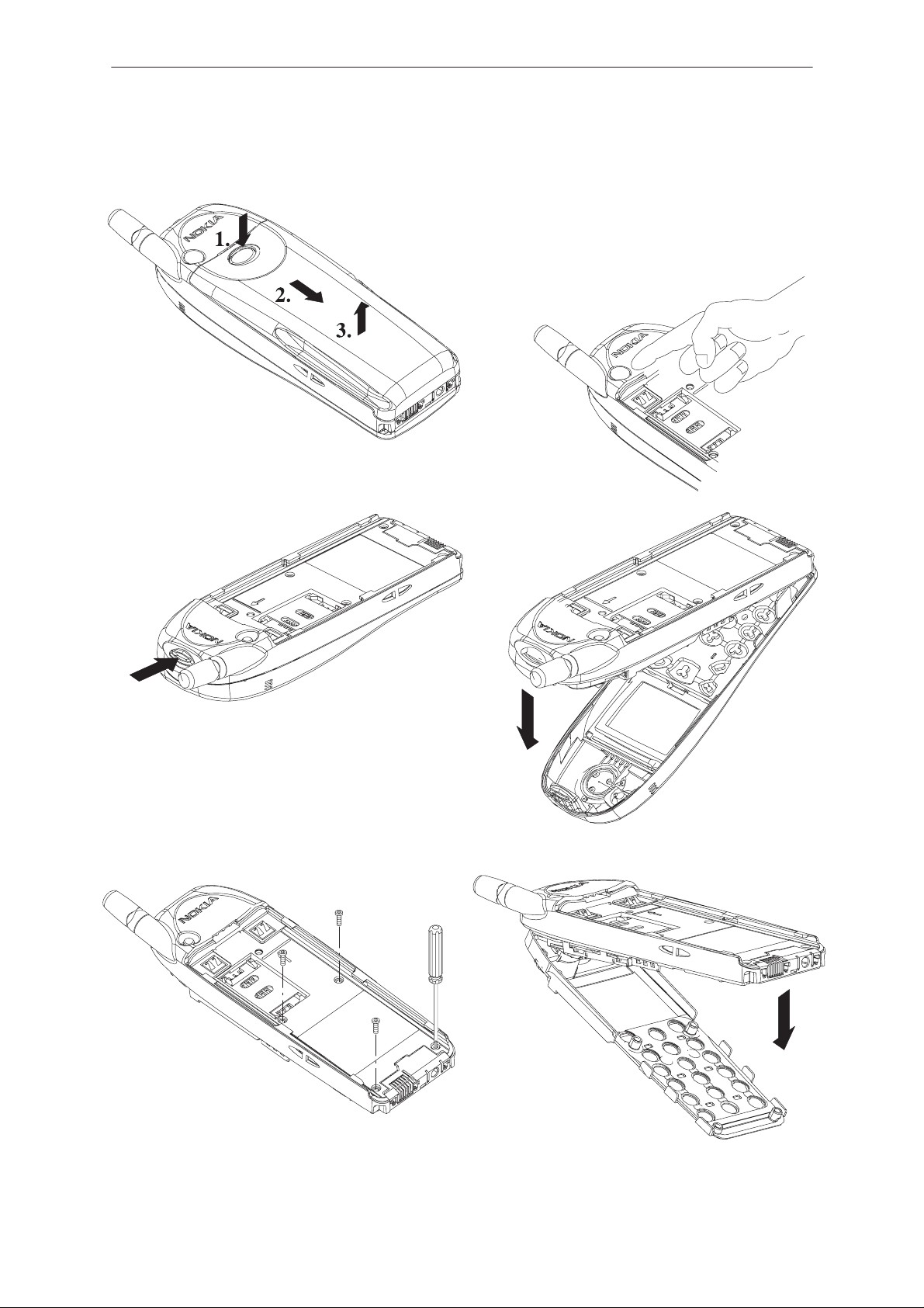
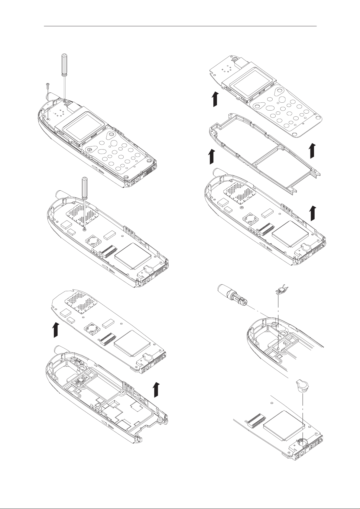
Disassembly
Press strongly towards
arrow direction
Disassembly & Troubleshooting Instructions
Remove battery
Remove dust cap by fingernail
Remove back cover
screws (4 pcs)
Carefully remove A–cover
Note snap fixings !
Remove C–cover
Original 03/98
Page 3
Page 4
NSE–1
PAMS
Disassembly & Troubleshooting Instructions
Remove UI–module
screws (2 pcs)
Remove UI–module
and frame
Remove engine
module screw (1 pc)
Technical Documentation
Remove engine module
Remove RTC–battery
Remove antenna by
pulling it straight out
Remove microphone
Page 4
Original 03/98
Page 5

PAMS
NSE–1
Technical Documentation
Trouble Shooting
The following hints should facility finding the cause of the problem when
the circuitry seems to be faulty. This trouble shooting instruction is divided following section.
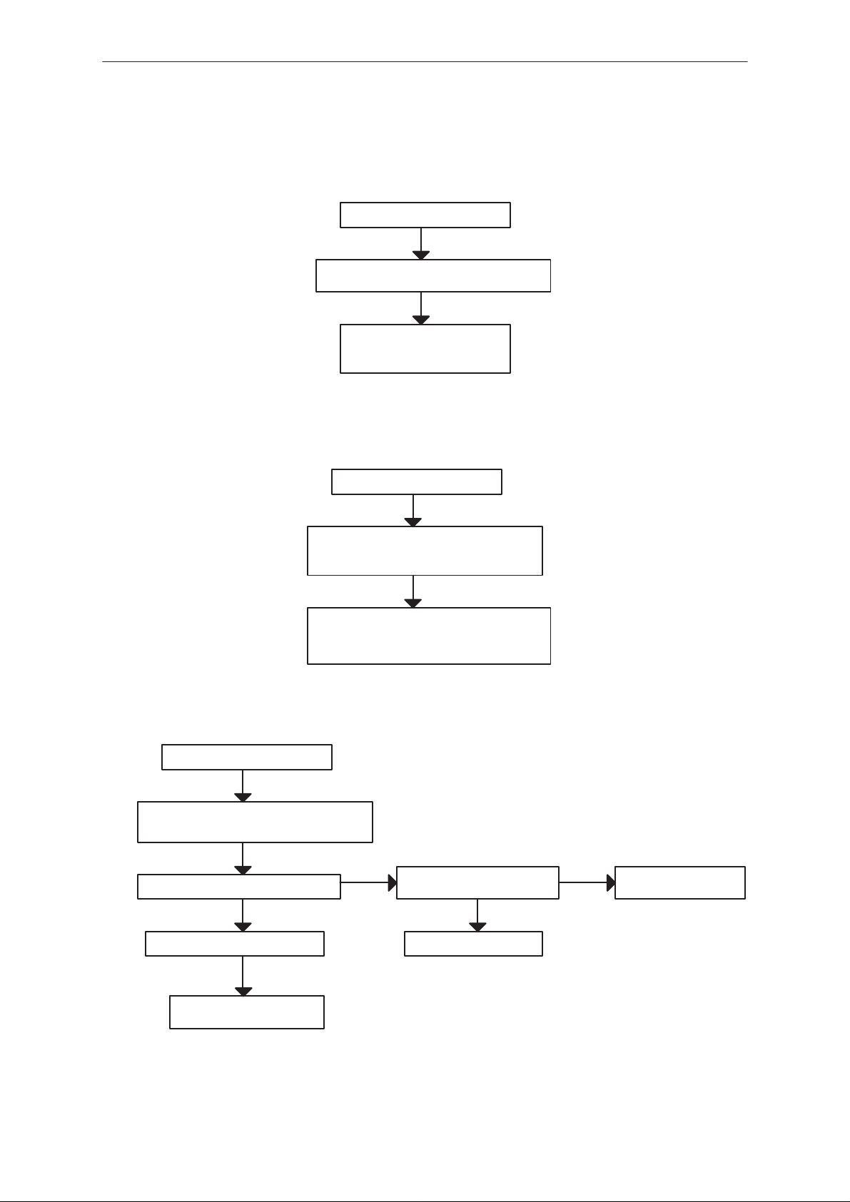
1. Phone is totally dead
2. Flash programming doesn‘t work
3. Power doesn‘t stay on or the phone is jammed
4. Display information: Contact Service
5. Phone doesn‘t register to the network or phone doesn‘t make a call.
6. Plug in SIM card is out of order ( insert SIM card or card rejected).
7. Audio fault.
8. Charging fault
The first thing to do is carry out a through visual check of the module. En-
sure in particular that:
a) there are not any mechanical damages
b) soldered joints are OK
Disassembly & Troubleshooting Instructions
Original 03/98
Page 5
Page 6

NSE–1
PAMS
Disassembly & Troubleshooting Instructions
Phone is totally dead
This means that phone doesn’t take current at all when the power switch
is pressed or when the watchdog disable pin (N100 pin 29) is grounded.
Used battery voltage must be higher than 3.0 V. Otherwise the hardware
of CCONT (N100) prevents totally to switch power on.
Phone is totally dead
YES
J232
VBAT is 3.6 V
YES
Voltage at pin 29 of CCONT (N100)
is 3.6 V
YES
NO Failure in VBAT line
Check X101, X102, L103
NO
Faulty circuit N100
Technical Documentation
N100 pin 55 (VBB) 2.8 V
N100 pin 25 (VXO) 2.8 V
when PWR switch is pressed
or watchdog disable pin is grounded
YES
See section: Power Doesn’t Stay On
NO
CCONT (N100) pin 29 0V
when PWR switch is pressed
Faulty circuit N100
Flash programming doesn’t work
In service places flash programming can be done via system connector
X100.
In flash programming error cases the flash prommer can give some information about a fault.
The fault information messages could be:
– MCU doesn’t boot
– Serial clock line failure
– Serial data line failure
– External RAM fault
– Algorithm file or alias ID don’t find
– MCU flash Vpp error
YES
NO
Check R118, X300
Check UI module
Page 6
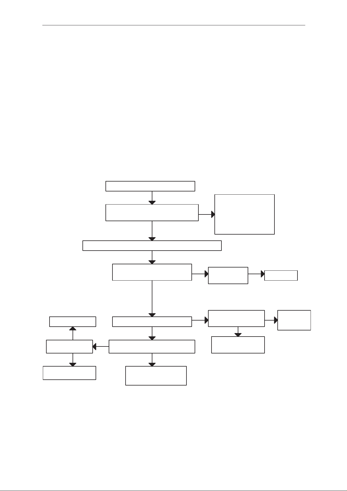
In cases that the flash programming doesn’t succeed there is a possibility
to check short circuits between the memories and the MCU (MAD2).
This test is useful to do, when the fault information is: MCU doesn’t boot,
Serial clock line failure or Serial data line failure.
Original 03/98
Page 7
PAMS
NSE–1
Technical Documentation
The test procedure is following:
1. Connect the short circuit wire between the test points J229 and J230.
2. Switch power on
3. If the voltage level in testpoint J225 is 2.8 V (”1”), the interface is OK. If
there is a short circuit, the voltage level in testpoint J225 stays low and
32kHz square wave signal can be seen in the lines which are already tested.
One must be noticed that this test can be found only short circuits, not
open pins.
Also upper data lines (15:8) of flash circuit D210 are not included to this
test.
Disassembly & Troubleshooting Instructions
CCONT pin 54
( PURX )
passed
MAD pin 38
MAD pin 134
J225
( MCUAD0)
( ExtSysResX))selftest
Original 03/98
Page 7
Page 8
NSE–1
PAMS
Disassembly & Troubleshooting Instructions
Flash Programming failure (1)
Flash programming doesn’t work
YES
If the fault information from the prommer is:
a) MCU doesn’t boot
b) serial data line failure
c) serial clock line failure
connect:
connect the shortcircuit fire from N100 pin 29 to ground (watchdog)
OK
EEPROM (D240) pin 8 (VBB) 2.8 V
J522 (VXO) 2.8 V
YES
NO
Technical Documentation
VBAT is correct
3.6 V
YES
N100 is faulty
check C213, R213
YES
J506 (RFC) 13 MHz
800 mV min
NO
check buffer V705 and
VCXO G600
NO J228 sleep clock(SCLK)
J227 master reset (Purx) = ”1” (2.8 V)
YES
NO
MAD2 (D200) pin 93: 13 MHz sine wave
clock signal: 500 mVpp min.
YES
or over loaded PurX line
Check that following lines are correct:
FCLK (MBUS) line: X100 pin 11 –> D200 pin 112
FTX (fbus_tx) line: X100 pin 13 –> D200 pin 104
FRX (fbus_rx) line: X100 pin 12 –> D200 pin 109
check also pullup and pulldown resistors: R203, R201, R215
GND : X100 pin 14 –> GND
OK
Enable the selftest function of D200 by connecting
shortcircuit between testpoints J229 and J230
Connect an oscilloscope to testpoint J225 and switch
power on
Voltage level rises to ”1” after power on at testpoint J225
YES
square wave 32 kHz
YES
Faulty circuit N100
NO
There is a shortcircuit
somewhere in memory control
lines or MCU address lines or
MCU lower (7:0) data lines
check sleep
NO
clock circuitry
(B100, R154...)
Page 8
There could be open pins in circuits D200 (D211, D240)
If not, the PCB or D200 (D211, D240) is faulty
Original 03/98
Page 9
PAMS
NSE–1
Technical Documentation
Flash Programming failure (2)
Flash progrmming doesn’t work
If the fault information from the prommer is:
External RAM fault
Check pins of SRAM (D220)
Check control lines of SRAM:
RAMSelX ...
Flash progrmming doesn’t work
Disassembly & Troubleshooting Instructions
YES
YES
YES
If the fault information from the prommer is:
Algorithm file or alias ID don’t find, ID is unknown etc.
Check pins of FLASH (D210)
Check control lines and upper data lines (15:8)
of FLASH: ROM1SelX...
Flash progrmming doesn’t work
YES
If the fault information from the prommer is:
MCU flash Vpp error
YES
Vpp = 3 V in D210 pin 13 (or C212)
YES
Check components C212, R211
OK
NO
YES
Vpp > 4.5 V in testpoint J234
YES
Check UI regulator N201
NO
Check regulator N100
C132, V116, C131
Faulty component D210
Original 03/98
Page 9
Page 10
NSE–1
PAMS
Disassembly & Troubleshooting Instructions
Technical Documentation
Power doesn’t stay on, or phone is jammed
If this kind of fault has come after flash programming, there are most
probably open pins in ICs.
The soldered joints of ICs: D200 (MAD2), D210 (FLASH), N100
(CCONT), D221 (SRAM) are useful to check at first.
Normally the power will be switched of by CCONT (N100) after 30 seconds, if the watchdog of the CCONT can not be served by software.
The watchdog updating can be seen by oscilloscope at pin 50 (DataselX)
of CCONT.
In normal case there is a short pulse from ”1” –> 0 every 8 seconds.
The power off function of CCONT can be prevented by connecting a short
circuit wire from CCONT pin 29 to ground.
Power doesn’t stay on or phone is jammed
YES
CCONT watchdog is served?
(pin 50 pulses 1 –> 0)
NO
YES
software is able to run
check UI module
If power is switched off
after few seconds, check
BSI and BTEM lines
connect the shortcircuit fire from N100 pin 29 to ground (watchdog)
check C213, R213
YES
J506 (RFC) 13 MHz
800 mV min
NO
check buffer V705 and
VCXO G600
OK
EEPROM (D240) pin 8 (VBB) 2.8 V
J522 (VXO) 2.8 V
YES
J227 master reset (Purx) = ”1” (2.8 V)
YES
NO
MAD2 (D200) pin 93: 13 MHz sine wave
clock signal: 500 mVpp min.
YES
Open pins or faulty circuit:
D200, D210, D221, N100
R215
NO
VBAT is correct
3.6 V
NO J228 sleep clock(SCLK)
square wave 32 kHz
Faulty circuit N100
or over loaded PurX line
YES
YES
N100 is faulty
check sleep
NO
clock circuitry
(B100, R154...)
Page 10
Original 03/98
Page 11

PAMS
NSE–1
Technical Documentation
Disassembly & Troubleshooting Instructions
Display Information: Contact Service
This fault means that software is able to run and thus the watchog of
CCONT (N100) can be served.
Selftest functions are run when power is switched on and software is
started to excute from flash.
If any of selftests is failed, contact service information will be shown on
display.
The phone doesn’t register to the network or phone
doesn’t make a call
If the phone doesn’t register to the network or the phone doesn’t make a
call, the reason could be either the baseband or the RF part.
The phone can be set to wanted mode by WinTesla service software and
determinate if the fault is in RF or in baseband part (RF interface measurements).
The control lines for RF part are supplied both the System Asic
(MAD2;D200) and the RFI (Cobba; N250). MAD2 handles digital control
lines ( like synthe, TxP etc.) and Cobba handles analog control lines (like
AFC, TxC etc.).
The DSP software is constructed so that operation states of DSP (MAD2)
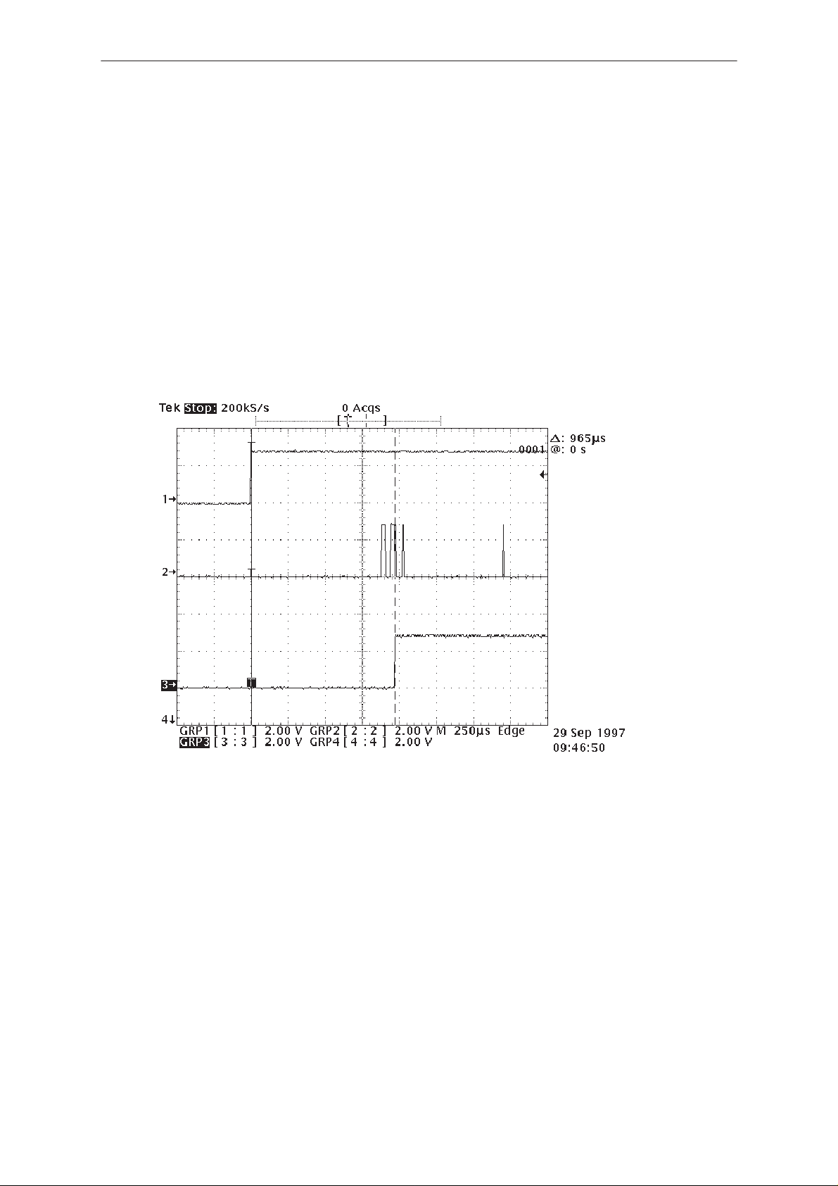
can be seen in external flag (DSPXF) output pin (D200 pin 91).
After power up, DSP signals all completed functions by changing the state
of the XF pin (see figures 39 and 40).
1. DSP initialization done
2.Synchronization to network
done
3. Registrarition to network
done.
1 2 3
Original 03/98
MAD2 pin 91 (DSPXF)
J222
Page 11
Page 12

NSE–1
PAMS
Disassembly & Troubleshooting Instructions
init
initialize
1
patch code
download
2
dsp
constants
download
initialization
done
Technical Documentation
MAD2 pin 91 (DSPXF)
J222
channel
scan starts
PSW
search last PSW
OK
3
send RACH
RACH OK
go SDCCH
imediate assigment
OK
synchronization
OK
MAD2 pin 91 (DSPXF)
J222
MAD2 pin 91 (DSPXF)
J222
Page 12
Original 03/98
Page 13

PAMS
NSE–1
Technical Documentation
Phone register failure
Phone doesn’t register to the network
Analog supply voltage VCOBBA is >2.7 V
at pin 7,12 ... of Cobba (N250)
Analog reference voltage Vref is 1.5 V
Supply voltage VCP (N100 pin 32) > 4.8 V
Supply voltage VRX (N100 pin 9) > 2.7 V
Supply voltage VSYN_1 (N100 pin 15) > 2.7 V
Supply voltage VSYN_2 (N100 pin 4) > 2.7 V
Supply voltage VTX (N100 pins 11, 20) > 2.7 V
Disassembly & Troubleshooting Instructions
or
phone doesn,t make a call
YES
YES
at pin 9 of Cobba (N250)
YES
during the receiving slot
during the transmitting slot
Check
NO
N100
NO
Check
R270, R271
NO Check
N100, D200
YES
Synthesizer lines: SEna (N620 pin 56),
SClk (N620 pin 54)
SData (N620 pin 55)
pulses 0 –> 1 during receiving slot
YES
NO
Check
D200
RF control lines: RxC (N250 pin 18) 0 –> 2.3 Vmax during receiving slot
AFC (N250 pin 19) 0 – 1.2 V typ. during receiving slot
YES
Analog data signal RxIP (N250 pin 22) 0–> 1.5 V DC during receiving slot
Analog data signal RxIN (N250 pin 22) 0–> 1.5 V DC during receiving slot
Used benefit signal is biased to DC and its amplitude is 50 mVpp
nominal and frequency is 13 MHz
YES
NO
DAX signal (N250 pin 48) pulses 1 –> 0 during receiving slot
YES
RF control lines: TxC (N250 pin 17) 0 –> 2.3 Vmax during transmit slot
TxP (D200 pin 176) 0–>1 (2.8 V) during transmit slot
YES
NO
Check
N250
NO
Check
N250 if DC is failed
Check
RF part if benefit signal is failed
Check
N250
Check
NO
N250 if TxC is failed
Check
D200 if TxP is failed
Analog data signals: TxIN (N250 pin 13) 0–> 0.8 V DC during transmit slot
Original 03/98
TxIP (N250 pin 14) 0 –>0.8 V DC during transmit slot
TxQN (N250 pin 15) 0 –>0.8 V DC during transmit slot
TxQP (N250 pin 16) 0 –>0.8 V DC during transmit slot
Used benefit signal is biased to DC and its amplitude is 300 mVpp
nominal and frequency is 67 kHz
NO
YES
Check
N250
Check
RF part
Page 13
Page 14

NSE–1
PAMS
Disassembly & Troubleshooting Instructions
SIM card is out of order
The hardware of the SIM interface from MAD2 (D200) to the SIM connector (X302) can be tested without SIM card.
When the power is switched on and if the BSI line (X101;1) is grounded
by resistor, all the used lines (VSIM, RST, CLK, DATA) rises up to 5 V four
times. Thus ”Insert SIM card” faults can be found without SIM card.
The fault information ”Card rejected” means that ATR message (the first
message is always sent from card to phone) is sent from card to phone
but the message is somehow corrupted, data signal levels are wrong etc.
or factory set values (stored to the EEPROM) are not correct.
Technical Documentation
Page 14
Original 03/98
Page 15

PAMS
NSE–1
Technical Documentation
SIM Card failure
VSIM(36), DATAO(43),SIMRSTO(42) and SIMCLKO(38) lines
rises up to 5 V after power on at pins of N100 (CCONT)
SIMPWR(30), DATAA(44), SIMRSTA(40), SIMCLK(41) and SIMIOC(39) lines
rises up to 2.8 V after power on at pins of N100 (CCONT)
Disassembly & Troubleshooting Instructions
Insert SIM card fault
YES
Voltage level < 1.5 V
at pin 95 of D200 when
BSI resistor is connected
YES
VSIM, DATA, RESET and CLOCK lines
rises up to 5 V after power on at pins
of SIM card
NO
NO
NO
NO
Check
R120, R122, X101
C120, C160
YES
Check
SIM card and SIM reader
connectors
YES
Check
X302, R124, R125, R128
YES
faulty circuit
N100 (CCONT)
SIMCardPwr(129), SIMCardData(120), SIMCardRstX(127), SIMCardClk(126) and SIMCardIOC(128) lines
rises up to 2.8 V after power on at pins of D200 (MAD2)
NO
Check again that voltage level at pin 95 (SIMCardDetX) of D200 is lower than 1.5V
If it is, change D200
Card Rejected fault
YES
VSIM is according the specification
VSIM = 2.8 V min (with 3 V SIM card)
NO
faulty circuit
N100 (CCONT)
VSIM = 4.5 V min (with 5 V SIM card)
YES
The ATR data can be seen at pin 43
(CCONT, N100)
YES
The ATR data can be seen at pin 120
(MAD2, D200)
YES
SIMIOControl line (N100 pin 36) is ”1”
during the ATR message
NO
NO
NO
Check
X302, R124
Check
N100
Check
D200
YES
faulty PCB
Original 03/98
YES
Check D200
Page 15
Page 16

NSE–1
PAMS
Disassembly & Troubleshooting Instructions
Audio failure (1)
Uplink (microphone) and downlink (earphone) are broken
YES
Voltage at pin 107 of MAD2 (D200)
is 2.8 V (without external audio devices) HOOKDET
YES
Voltage at pin 108 of MAD2 (D200)
is 2.8 V (without external audio devices) HEADDET
YES
Frequency at pin 138 of MAD2 (D200)
is 1 MHz, square wave 2.8 Vpp
YES
Technical Documentation
NO
Check
R259, R260
NO
NO
Check
R257, R256, R261
Check
N250 (Cobba)
Frequency at pin 139 of MAD2 (D200)
NO
is 8 kHz, square wave pulses 2.8 Vpp
Uplink (microphone) is broken
YES
Voltage at pin 6 of X100 is 1.8 V
NO
Voltage at pin 7 of X100 is 0.3 V
during a call
YES
DC voltage at pins 59 and 60 of
NO Check
N250 is 1.4 V during a call
YES
Analog audio signal (few millivolts) at pins 59 and 60
of N250 during a call
YES
Digital PCM data at pin 137 of MAD2 (D200)
during a call
Check
N250 (Cobba)
Check
microphone, X100 and micbias
components V250...
If OK, check that micbias control line
is (D200 pin1 ) 2.8 V during a call
N250 (Cobba)
NO
Check
C262, C263 and PCB
routings
NO
Check
N250 (Cobba)
Page 16
Original 03/98
Page 17

PAMS
NSE–1
Technical Documentation
Audio failure (2)
Digital PCM data at pin 52 of Cobba (N250)
during a call
Analog audio signal (some ten millivolts) at pins 5 and
6 of N250 during a call
Disassembly & Troubleshooting Instructions
Downlink (earphone) is broken
YES
YES
DC voltage at pins 5 and 6 of
N250 is 1.4 V during a call
YES
NO
NO
N250 (Cobba)
Check
D200 (MAD2)
Check
NO
Check
N250 (Cobba)
Original 03/98
Page 17
Page 18

NSE–1
PAMS
Disassembly & Troubleshooting Instructions
Charger failure
Nothing happens when charger is connected
YES
Voltage level at pin 60 of CCONT (N100)
is higher than 0.4 V when charger is connected
YES
Check N100
Display Information: Not charging
YES
Voltage level at pin 62 of CCONT (N100)
is about 0.8 V when power is connected
BSI resistor value should be 39 k
YES
Technical Documentation
NO
Check
X100, F100, L104
R104, R103
NO Check
X101, R120, R122
Voltage level at pin 63 of CCONT (N100)
is about 0.5 V when power is connected
BTEMP resistor value should be 47 k
YES
32 Hz square wave frequency at pin 7 of CHAPS (N101)
YES
Voltage levels at pins 5 and 12 of CHAPS (N101)
are same as VB
YES
Voltage levels at pins 5 and 12 of CHAPS (N101)
rises when charger is connected
NO
X101, R120, R122
NO
NO
NO
Check
Check
N100
Check
R131, N101
Check
N101
Page 18
Original 03/98
Page 19

PAMS
NSE–1
Technical Documentation
Receiver Fault (1)
Change X540
NO
Ω
YES
and 2 ~ 0
Check soldered joints of X540
Loading between X540 pin 1
NO
and Z550, check also that X540
Change Z550
is assembled correct, if OK
Disassembly & Troubleshooting Instructions
NO
Ω
YES
if OK change Z500
Check soldered joints,
NO
Ω
YES
if OK change it
Z500 input, loading > 1 M
Check C500 soldered joints,
NO
if OK cange Z500
Check C518, C504,
NO
Ω
YES
Z500 output,
Change Z500
loading > 1 M
NO
loading 50
N500 pin 7 and 8,
C520 check
internal coils
Check soldered joints of C516,
NO
Change N500
change N500
Rise up N500
pin 7,8. If level
back to normal
YES
YES
Fault
Receiver
N500 pin 25, SL: –61 dBm
Duplexer ant–pin, SL: –58 dBm
NO
Ω
YES
N500 pin 25,
loading > 1 M
Duplexer Rx–pin, SL: –61 dBm
NO
NO
YES
N500 pin 23, SL: –38 dBmN500 pin 26 is ”HIGH”
NO
YES
NO
YES
Ω
YES
Z500 input, SL: –44 dBm
Z500 output, SL: –47 dBm
N500 pin 17 and 19, 2.8V
NO
YES
YES
N500 pin 16, 1.5V
NO
YES
1st IF
N500 pin 7 and 8, SL: –57 dBm
Ω
YES
N500 pin 20, loading 10 k
NO
Ω
YES
N500 pin 23, loading 10 k
NO
71 MHz
Original 03/98
change N500
Check C506, if OK
Change duplexer
N500 pin 26,
loading > 1 M
NO
Check PDATA0–line
for short circuits
Check PDATA0–line
D200 pin 171
VSYN_1(J516) lines
Check VRX(J510) and
from CCONT
Check VREF_2(J518)
voltage line
Check soldered joints of N500
and R504, if OK change R504
of pin 23, if OK change N500
Check components in line out
Page 19
Page 20

NSE–1
PAMS
Disassembly & Troubleshooting Instructions
Receiver Fault (2)
Z621
OK change
short circiuts, if
UHFLO
NO
YES
SL: –28 dBm
G530 Out, 1018 MHz
to N500 pin 12
Check connections from G530
Check input for
NO
Ω
loading > 1 M
Z621 input 1 and 2,
for short
Check output
NO
YES
line to Z621
Check components in input
Z621 ouput 1 and 2,
Technical Documentation
change Z621
circiuts, if OK
Ω
YES
loading > 1 M
change Z621
joints at N620, if OK
Check components in
output line. Check soldered
1st IF
71 MHz
NO
YES
N500 pin 12,
1018 MHz SL: –28 dBm
YES
SL: –28
N500 pin 9 and 10,
NO
YES
N500 pin 15,
N500 pin 6, 2.8V
NO
NO
NO
YES
SL: –30
Z621 input 1 and 2,
Ω
YES
loading 10 k
N500 pin 9 and 10,
NO
Ω
YES
loading 10 k
NO
SL: –43
Z621 output,
Change N500
YES
N620 pin 51(J530) and
NO
N620 pin 47, 2.8V
NO
YES
52(J532), SL: –43
YES
YES
DC–level ~1.7V
N620 pin 51 and 52,
NO
Ω
2nd IF
13 MHz
Change N620
Page 20
soldered joints
Check VRX(J510) and
Check R504
OK at pads change N500
Rise up 9 and 10, if loading
YES
of N620
Check soldered joints
loading 5 k
N620 pin 51 and 52,
NO
Original 03/98
52 for short circuit
Check N620 pin 51 and
Page 21

PAMS
NSE–1
Technical Documentation
Receiver Fault (3)
VHFLO
Check VRX supply voltage
NO
~2.8V
N620 pin 47(J510),
Check RXC control voltage
NO
YES
N620 pin 53(J554),
from COBBA pin 18
~1.2V
Disassembly & Troubleshooting Instructions
Change N620
NO
YES
Change N620
YES
DC–level ~1V
N620 pin 29 and 30,
2nd IF
13 MHz
NO
N620 pin 8(J542),
NO
YES
SL: – 28 dBm
YES
N620 pin 44,
SL: – 19 dBm
YES
SL: –26 dBm
Z620 input(J540),
NO
joints
Check R626 and soldered
YES
SL: –28 dBm
Z620 output(J538),
NO
change Z620
Check soldered joints, if OK
NO
YES
and pin 35, SL: –33 dBm
N620 pin 34, SL: –36 dBm
NO
YES
DC–level, ~1.4V
N620 pin 34 and 35,
YES
SL: – 29 dBm
N620 pin 29 and 30,
Check R628 and R629
Check soldered joints at N620
and N250, if OK change N620
YES
SL: –29 dBm
N250 pin 22 and 23,
NO
N620 and N250
Check connections between
COBBA
Original 03/98
NO
N620
Change
Page 21
Page 22

NSE–1
PAMS
Disassembly & Troubleshooting Instructions
Receiver Fault (4)
COBBA
N250 pin 7,12,21,25 and 63,
~2.8V
YES
N250 pin 27 and 53,
~2.8V
YES
N250 pin 9,
~1.5V
YES
N250 pin 10,
loading 100 k
YES
N250 pin 45,
13 MHz clock OK
YES
Ω
NO
NO
NO
NO
NO
Check VCOBBA–voltage from
Check VBB–voltage from
Check VREF–voltage from
CCONT pin 13 through R253
Check soldered joints and
Check COBBACLK–line from
Technical Documentation
CCONT pin 22
CCONT pin 55
R253
MAD pin 144
N250 pin 28,
is ”HIGH”
YES
Check data and adress lines
between D200 and N250, if
OK change N250
COBBACLK – signal:
Oscilloscope picture in Appendix A
NO
Check COBBARSTX–line
from MAD pin 163
Page 22
Original 03/98
Page 23

PAMS
NSE–1
Technical Documentation
Receiver Fault (5)
UHFLO
G530 VCC–pin voltage, 2.8V
YES
G530 VC(J500) voltage
~2.25V (Mid CH)
YES
Change G530
Disassembly & Troubleshooting Instructions
NO
Check VSYN_1–line and R530
NO
Check soldered joints
at G530, N620 and components
N620 pin 21, 13 MHz clock
in VC–line
Does G530 oscillate at
any frequency
N620 pin 9,22 and 25,
N620 17 and 28,
2.8V
5V
YES
YES
YES
YES
YES
NO
NO
NO
NO
Change G530
Check C633 and
soldering joints at
Check VSYN_2(J508)
from CCONT and
CNTVR3–control from MAD
Check VCP–voltage
from CCONT pin 32
N620
N620 pin 58,
1.5V
N620 pin 59,
loading 15 k
working OK
SCLK, SDATA, SENA1
Change N620
13 MHz clock oscilloscope picture in Appendix A
SCLK, SDATA, SENA1 oscilloscope pictures in Appendix B
YES
YES
YES
NO
NO
Ω
NO
Check VREF_1–line
Check soldering joints
at N620 and R635, if
OK change R635
Check SCLK, SDATA,
SENA1–lines from
MAD
Original 03/98
Page 23
Page 24

Page 24
VHFLO
Receiver Fault (6)
Disassembly & Troubleshooting Instructions
NSE–1
N620 9,22 and 25, ~2.8V
Original 03/98
N620 pin 18, ~2.3V
YES
N620 17 and 28, ~5V
YES
Change N620
NO
NO
NO
Does the VCO oscillate at any
frequency ?
YES
Check VSYN_2(J508)
supply voltage
Check VCP voltage line
NO
V581 collector,
~2.6V
YES
V581 base, ~1.7V
YES
V581 emitter, ~1V
YES
Check V580, L581, C582,
C583
NO
NO
NO
Check VSYN_1(J516) supply
voltage line to V581
Check R581, R585 and
soldered joints
V581 emitter loading ~330
Ω
if OK change V581
,
Technical Documentation
PAMS
Page 25

Original 03/98
AFC
Receiver Fault (7)
Technical Documentation
PAMS
RSSI tuning working OK ?
YES
N250 pin 19,
voltage between 0.5 – 2.3V
YES
Set SpectrumAnalyzer
Frequency: 13 MHz
Span: 10 kHz
RESBW: 3 kHz
13 MHz in midst,
(Test point J 506)
NO
NO
Use sevice software to set AFC
NO
Receiver
Fault
N250 pin 19,
loading > 1 M
YES
Change N620
to MAX
Ω
NO
Check AFC–line(J520) for
short circuits, if OK change
Disassembly & Troubleshooting Instructions
Page 25
NOTE !
properly, supply voltages stays
down.
If DSP in MAD does not work
AFC–voltage(J520),
~2.3V
YES
Main clock(J506),
> 13 MHz
NO
NO
Check R600 and C602, if
OK change N250
NSE–1
Change G600
Page 26

NSE–1
PAMS
Disassembly & Troubleshooting Instructions
Transmitter Fault (1)
& J560)
from CCONT
Check TXP–line from MAD
Check VTX supply voltage
NO
YES
N620 pin 1,
TXP–pulse OK?
OK ?
N620 pin 63(J514), VTX–pulse
VHFLO
Check TXQP, TXIP, TXQN, TXIN
lines from COBBA pin 13...16 and
soldered joints at N620 and N250,
if OK change N250(Test pins J558
NO
N620: TXQP, TXQN, TXIP
NO
YES
and TXIN, OK ?
Check VREF_1 – line
Check TXC–line from COBBA
NO
YES
NO
YES
N620 pin 58, ~1.5V
N620 pin 11, TXC–pulse OK?
Technical Documentation
joints
Change N620
Check R635 and soldered
NO
YES
NO
Ω
YES
N620 pin 59,
loading 15 k
N620 pin 61 and 62, ~0.8V
TXQP, TXIP, TXIN, TXQN, TXP and VTX:
Oscilloscope pictures in Appendix C
Fault
TXLEV 5
Transmitter
NO
N620 pin 8(J542)
NO
YES
N620 pin 61 and 62,
232 MHz SL: –28 dBm
116 MHz SL: –40 dBm
YES
YES
N500 pin2(J552) and pin3
(J550) 116 MHz SL: –32 dBm
NO
Ω
YES
loading > 1M
N500 pin 2 and 3,
NO
YES
SL: –28 dBm
N500 pin 12(RX–Continous),
NO
UHFLO
change N500
Check C652, C653, C655,
L623, L624, R623, R625, if OK
YES
SL: –18 dBm
N500 pin 30,
NO
YES
~2.8V
N500 pin 16,
N500 pin 1 and 29,
NO
NO
~1.5V
YES
N500 pin 20,
NO
1
Transmitter
Ω
YES
loading 10 k
Change N500
Page 26
OK change N500
3 for short circuits, if
Check N500 pin 2 and
from CCONT
Check VTX supply voltage
Check VREF_2 – line(J518)
joints
Check R504 and soldered
Original 03/98
Page 27

Original 03/98
Transmitter
1
TXLEV5
Transmitter Fault (2)
Technical Documentation
PAMS
Page 27
Check Z505 output for short
circuits, if OK change Z505
Check VBATT–connections to
N550
Check soldered joints
at N550
Check soldered joints at N550
and N620, if OK change N620
VTX and power contol pulse(TXC):
Oscilloscope pictures in Appendix D
NO
Z505 output,
loading > 1 M
YES
Change Z505
NO
N550 pin 2,4,6,12,13 and 14
NO
NO
C564,C505,C566,C572,C555,C
567,L552, if OK change N550
~3.6V
YES
N550 pin 1 and 16,
VTX–pulse
YES
N550 pin 9,
power control pulse
YES
Check
Z505 input,
SL: – 23 dBm
YES
NO
Ω
NO
Z505 output,
SL: –29 dBm
YES
N550 pin 8,
SL: –29 dBm
YES
N550 pin 13,
SL: –2 dBm
YES
Duplexer TX–pin,
SL: 6 dBm
YES
RF–connector X540 pin 1,
SL: 5 dBm
NO
NO
NO
NO
Z505 input,
loading > 1 M
Check C700
Check V640 limiter circuit
DC–levels(VTX–voltage),
Base: ~0.6V
Collector: ~0.6V
Emitter: ~0.3V
Check components in line
from N550 to Z550. Also
check for short circuits, if OK
change Z550
Check X540, if OK change
Ω
YES
Z550
NO
Check Z505 input for short
circuits, if OK change Z505
Check R668, R662, R664,
R666, R670, C660, C662
and C562, If OK change
V640
Disassembly & Troubleshooting Instructions
NSE–1
Page 28

NSE–1
PAMS
Disassembly & Troubleshooting Instructions
Transmitter Fault (3)
Power
Control
TXLEV5
Transmitter working OK
YES
N250 pin 11,
TXC – pulse OK
NO
NO
Check TXC – line from N250
Transmitter
pin 17, if OK change N250
Technical Documentation
Fault
YES
N620 pin 11 and 12 pulses
are about the same
NO
R554, if OK change V550
V550 anode,
DC–voltage ~0.8V
YES
N620 pin 12,
loading ~4 k
YES
Check C554, R553 and
Ω
NO
NO
Check VSYN_1 voltage
through R550, R551 and R552
Check C632, if OK
change N620
TXC – pulse:
Oscilloscope picture in Appendix D
Page 28
Original 03/98
Page 29

PAMS
NSE–1
Technical Documentation
Appendix A
Disassembly & Troubleshooting Instructions
Picture 1. COBBACLK – signal
Picture 2. 13 MHz Main clock – signal
Original 03/98
Page 29
Page 30

NSE–1
PAMS
Disassembly & Troubleshooting Instructions
Appendix B
Picture 3. SCLK – signal
Technical Documentation
Picture 4. SDATA – signal
Picture 5. SENA1 – signal
Page 30
Original 03/98
Page 31

PAMS
NSE–1
Technical Documentation
Disassembly & Troubleshooting Instructions
Appendix C
Picture 6. TXQP, TXQN, TXIP and TXIN – signal
Picture 7. TXP – signal
Picture 8. VTX – signal
Original 03/98
Page 31
Page 32

NSE–1
PAMS
Disassembly & Troubleshooting Instructions
Appendix D
Technical Documentation
Picture 9. TXC – signal (TXLEV5)
Picture 10. DET – signal(N620 pin 12) TXLEV5
Page 32
Original 03/98
 Loading...