

Page 1

CCS Technical Documentation
NPM-6/6X Series Transceivers
Troubleshooting Instructions
Issue 2 06/03 Copyright Nokia. All rights reserved.
Page 2

NPM-6/6X Company confidential
Troubleshooting Instructions CCS Technical Documentation
[This page left intentionally blank]
Page 2 Copyright Nokia. All rights reserved. Issue 2 06/03
Page 3

Company confidential NPM-6/6X
CCS Technical Documentation Troubleshooting Instructions
Table of Contents
Page No
RF Troubleshooting ....................................................................................................... 4
Introduction to RF troubleshooting .............................................................................4
RF Key component placement .....................................................................................5
RF Measurement points ...............................................................................................6
EGSM900 & GSM1800 Transmitter ............................................................................. 7
General instructions for Tx troubleshooting ............................................................. 7
Transmitter troubleshooting diagram ........................................................................ 9
Pictures of transmitter signals ................................................................................. 12
EGSM900, GSM1800 and GSM1900 Receiver .......................................................... 14
General instructions for Rx troubleshooting ........................................................... 14
Troubleshooting diagram for EGSM900 receiver................................................... 18
Troubleshooting diagram for GSM1800 receiver ................................................... 19
Troubleshooting diagram for GSM1900 receiver ................................................... 20
Synthesizer ................................................................................................................... 21
General instructions for synthesizer troubleshooting.............................................. 21
Synthesizer troubleshooting diagram ...................................................................... 22
Pictures of synthesizer signals................................................................................. 23
Baseband Troubleshooting........................................................................................... 25
BB Measurement points ............................................................................................25
Troubleshooting diagrams .........................................................................................27
FM Radio troubleshooting ........................................................................................... 48
FM Radio component layout .....................................................................................48
FM Radio troubleshooting diagram ...........................................................................50
Notes to "FM Radio troubleshooting diagram"....................................................... 50
Issue 2 06/03 Copyright Nokia. All rights reserved.. Page 3
Page 4

NPM-6/6X Company confidential
Troubleshooting Instructions CCS Technical Documentation
RF Troubleshooting
Introduction to RF troubleshooting
Measurements should be done using Spectrum analyzer with high-frequency highimpedance passive probe (LO-/reference frequencies and RF power levels) and Oscilloscope with a 10:1 probe (DC-voltages and low frequency signals)
The RF-section is built around one RF-ASIC (HELGA N500). For easier troubleshooting,
this RF troubleshooting document is divided in to sections.
Before changing HELGA, please check following things: Supply voltages are OK and serial
communication is coming from baseband to HELGA.
Please note that the grounding of the PA module is directly below PA-module so it is difficult to check or change. Most RF semiconductors are static discharge sensitive! So
ESD protection must be taken care of during repair (ground straps and ESD soldering
irons). HELGA and PA are moisture sensitive so parts must be pre-baked prior to soldering.
Apart from key components described in this document here are a lot of discrete components (resistors, inductors and capacitors) which troubleshooting is done by checking if
soldering of the component is done properly (for factory repairs checking if it is missing
from PWB). Capacitor can be checked for shortening and resistors for value by means of
an ohmmeter, but be aware in-circuit measurements should be evaluated carefully.
Please be aware that all measured voltages or RF levels in this document are rough figures. Especially RF levels varies due to different measuring equipment or different
grounding of the used probe. When using RF probe usually a good way is to use metallic
tweezers to connect probe ground to PWB ground as close to measurement point as possible.
Page 4 Copyright Nokia. All rights reserved. Issue 2 06/03
Page 5
Company confidential NPM-6/6X
CCS Technical Documentation Troubleshooting Instructions
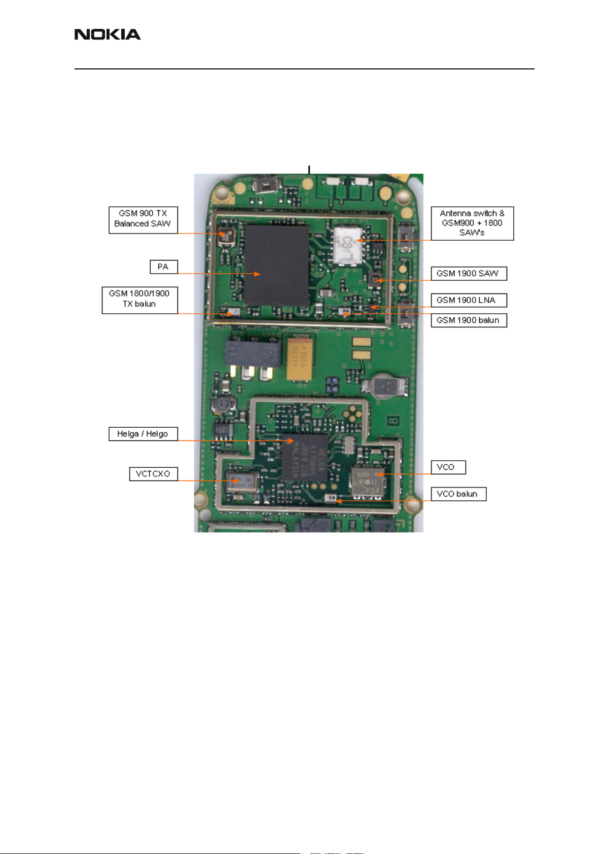
RF Key component placement
Figure 1: Component placement 1
Issue 2 06/03 Copyright Nokia. All rights reserved.. Page 5
Page 6
NPM-6/6X Company confidential
Troubleshooting Instructions CCS Technical Documentation
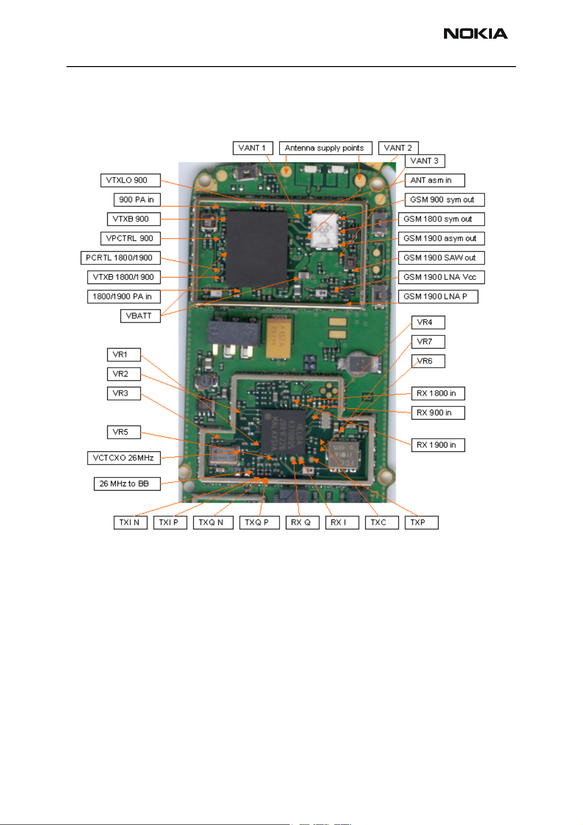
RF Measurement points
Figure 2: Component placement 2
Page 6 Copyright Nokia. All rights reserved. Issue 2 06/03
Page 7

Company confidential NPM-6/6X
CCS Technical Documentation Troubleshooting Instructions
EGSM900 & GSM1800 Transmitter
General instructions for Tx troubleshooting
Kindly refer to the Service Software Section, Service Concept dagram (p.40)
Connect test jig to computer with DAU-9S cable or to FPS-8 Flash Prommer with XCS-4
modular cable.
Make sure that you have PKD-1 dongle connected to computers parallel port.
Connect DC power supply to module test jig with FLC-2 cable.
Attention: When repairing or tuning transmitter use external DC supply with at
least 3A current capability. Set the DC supply voltage to 3.9V and set the jumper con-
nector on test jig to "bypass" position.
Connect a RF-cable to the module test jig (MJS-49) RF connector to and to measurement
equipment or at least 10dB attenuator, otherfwise the PA may be damaged. Normally
Spectrum analyzer is used as measurement equipment.
Attention: Normally Spectrum analyzer maximum input power is +30dBm. It is recommended to use 10dB attenuator on Spectrum analyzer input to prevent damage.
Set the phone module to test jig and start Phoenix service sofware
Initialize connection to phone. (use FBUS driver when using DAU9S and COMBOX driver
when using FPS-8)
Select product from the menu
File -> Choose product -> NPM-6
From toolbar set operating mode to "Local"
Activate RF controls window from the menu
Maintenance -> Testing -> RF Controls
From the RF controls window
- Select band "EGSM900" or "GSM 1800" or "GSM1900" (Default = "EGSM900")
- Set Active unit to "Tx" (Default = "Rx")
- Set Operation mode to "Burst" (Default = "Burst")
- Set Tx data type to "Random" (Default = "All1")
Issue 2 06/03 Copyright Nokia. All rights reserved.. Page 7
Page 8

NPM-6/6X Company confidential
Troubleshooting Instructions CCS Technical Documentation
- Set Rx/Tx channel to 37 on EGSM900 band or 700 on GSM1800 band or 661 on
EGSM1900 (Defaults)
- Set Tx PA mode to "Free" (Default)
- Set power level to 5 (Default = 19) on EGSM900 or to 0 (Default = 15) on GSM1800 or
GSM1900
Page 8 Copyright Nokia. All rights reserved. Issue 2 06/03
Page 9

Company confidential NPM-6/6X
(EGSM900
CCS Technical Documentation Troubleshooting Instructions
Transmitter troubleshooting diagram
Figure 3: Transmitter troubleshooting
TX troubleshooting
Check output signal level:
+32...+33dBm @897.4 MHz (GSM900)
+29...+30dBm @1747.8 MHz
(GSM1800 & GSM1900)
Check with RF probe
signal level on
PA input >=0dBm (*
start TX power level
tuning and check
tuned RAC values:
Highest level~700...900
Lowest level ~190...210
Base levle ~160...190
Major differences ?
OK ?
TX signal found ?
Yes
OK ?
Yes
No
Check output signal
on 500 MHZ span
Signal found on
incorrect frequency ?
No
*(When 1kOhm passive probe is used,
correct the measurement result by +26dB
Yes
TX OK
Yes
Yes
Check
all power
levels,
OK ?
No
HELGA
troubleshooting
Tune Tx DAC values
No
Yes
Tune
TX power
levels,
OK ?
Synthesizer
troubleshooting
No
Check with oscilloscope:
PA ctrl voltage
>1.5V peak OK ?
Yes
PA & ant switch
troubleshooting
Check control loop
components
No
Yes
Replace
faulty
component(s)
OK ?
Yes
Replace HELGA
dead
Issue 2 06/03 Copyright Nokia. All rights reserved.. Page 9
Page 10
NPM-6/6X Company confidential
Troubleshooting Instructions CCS Technical Documentation
Figure 4: HELGA IC troubleshooting
HELGA
troubleshooting
Check with oscilloscope:
-TXI/TXQ signals
--VR1, VR2, VR4, VR5, VR6 = 2.8V
-VrefRF01 = 1.35 V
-HELGA serial interface
-TXP & TXC signals
OK ?
No
Baseband
troubleshooting
Check with RF probe:
Check with RF probe:
-4GVCO out signal
-4G VCO out signal
- 3589.6 MHz (GSM900)
-3589.6MHz (EGSM900)
-3495.6 MHz (GSM1800)
-3495.6 MHz (GSM1800)
- 3760 MHz (GSM1900)
-3760 MHz (GSM1900)
Level >-10dBm (*
Level >-10dBm
OK ?
Check modulator
output components
OK ?
Replace
faulty
component(s)
No
Synthesizer
troubleshooting
*(When 1kOhm passive probe is used,
correct the measurement result by +26dB
Yes
Replace HELGA
dead
Page 10 Copyright Nokia. All rights reserved. Issue 2 06/03
Page 11
Company confidential NPM-6/6X
CCS Technical Documentation Troubleshooting Instructions
Figure 5: PA and Antenna Switch troubleshooting
PA & ant switch
troubleshooting
*(When 1kOhm passive probe is used,
Yes
correct the measurement by +26dB
Check with RF probe
signal level on
PA input >=0dBm (*
OK ?
Yes
Check with
oscilloscope:
-VBATT ~4V
- VTXB = 2.8 V pulsed
- VTxLO_GSM = 0V (GSM900)
(EGSM900)
OK ?
Yes
No
Replace
PA
Check components
around PA
OK ?
Yes
Yes
Check with
oscilloscope:
-VANT_1 (GSM900)
-VANT_1 (EGSM900)
-VANT_2 (GSM1800)
-VANT_2 (GSM1800)
-VANT_3 (GSM1900)
-VANT_3 (GSM1900)
OK ?
No
Check
VANT lline components
OK ?
Yes
Replace
HELGA
Replace
ant. switch
No
Replace
faulty
component(s)
No
Replace
faulty
component(s)
Issue 2 06/03 Copyright Nokia. All rights reserved.. Page 11
Page 12
NPM-6/6X Company confidential
v
Troubleshooting Instructions CCS Technical Documentation
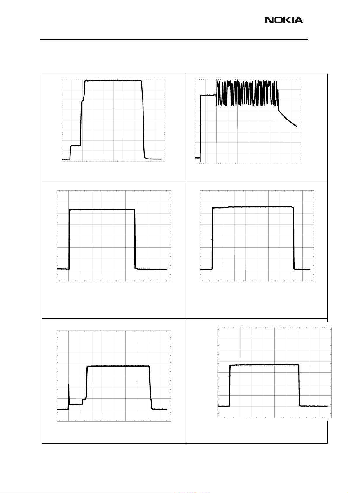
Pictures of transmitter signals
Figure 6: Transmitter signals
TXI
VPC
200mV/div
1
VPCTRL _900 power level high at R703/C703
VPCTRL_1800/1900 power level high at R704/C704
500mV/div 100us/div
VANT_1 / EGSM900 TX at C804
VANT_2 / GSM1800 TX at C835
100us/di
VANT_3 / GSM1900 TX at C805 OV
( no signal/ Flatline on Oscilloscope screen)
200mV/div
100us/div
TX I/Q at R516/517 power level high Random data
_
1
500mV/div 100us/div
VANT_1,VANT_2,VANT_3
500mV/div MTB 100us/div
VTXB_900 at C713
VTXB_1800_1900 at C714
500mV/div 100us/div
TXP at J504
Page 12 Copyright Nokia. All rights reserved. Issue 2 06/03
Page 13
Company confidential NPM-6/6X
CCS Technical Documentation Troubleshooting Instructions
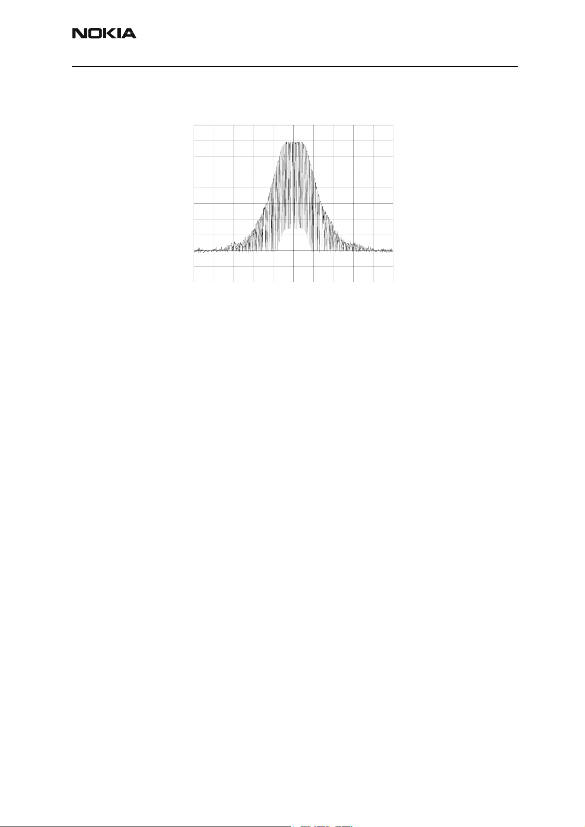
Figure 7: TX OUT signal
GS MPOW Tue Sep 25 13: 48: 59 2001
REF 4 1. 0 d Bm ATT 4 0 d B
10dB/
REF OFS
11. 0 dB
RBW
100 kHz
VBW
100 kHz
SWP
2. 0 s
CENTER 897. 400 MHz SPAN 2. 000 MHz
Tx out signal, 900 band, burst mode, channel 37
A_wr i t eB_bl ank
Issue 2 06/03 Copyright Nokia. All rights reserved.. Page 13
Page 14

NPM-6/6X Company confidential
Troubleshooting Instructions CCS Technical Documentation
EGSM900, GSM1800 and GSM1900 Receiver
General instructions for Rx troubleshooting
Connect test jig to computer with DAU-9S cable or to FPS-8 Flash Prommer with XCS-4
modular cable.
Make sure that you have PKD-1 dongle connected to computers parallel port.
Connect DC power supply to module test jig with FLC-2 cable.
Set the DC supply voltage to 6V (test jig has internal voltage regulator of output voltage 4V).
Connect an RF-cable to the module test jig (MJS-49) RF connector and to RF signal generator.
Set the phone module to test jig and start Phoenix service sofware.
Initialize connection to phone. (use FBUS driver when using DAU9S and COMBOX driver
when using FPS-8)
Choose product from the menu
File -> Choose product -> NPM-6
From toolbar set operating mode to "Local"
Activate RF controls window from the menu
Maintenance -> Testing -> RF Controls
From the RF controls window:
- Select band "EGSM900", "GSM 1800" or “GSM1900” (Default = "EGSM900")
- Set Active unit to "Rx" (Default = "Rx")
- Set Operation mode to "Burst" (Default = "Burst")
For continuous mode:
- Set Operation mode to "Continuous"
- Set AGC to "12: FEG_ON + DTOS_ON + BB_30=Vgain60” (maximum gain setting used
in normal mode)
(Default = "14: FEG_ON + DTOS_ON + BB_42=Vgain72")
Page 14 Copyright Nokia. All rights reserved. Issue 2 06/03
Page 15
Company confidential NPM-6/6X
CCS Technical Documentation Troubleshooting Instructions
- Set Rx/Tx channel to 37 on EGSM900 band, 700 on GSM1800 band or 661 on
GSM1900 (Defaults)
Apply 942.46771 MHz (channel 37 + 67.710 kHz offset), 1842.86771 MHz (channel 700
+ 67.710 kHz offset) or 1960.06771 MHz (channel 661 + 67.71 kHz) –90 dBm signal to
the RF-connector (remember to compensate for cable attenuation).
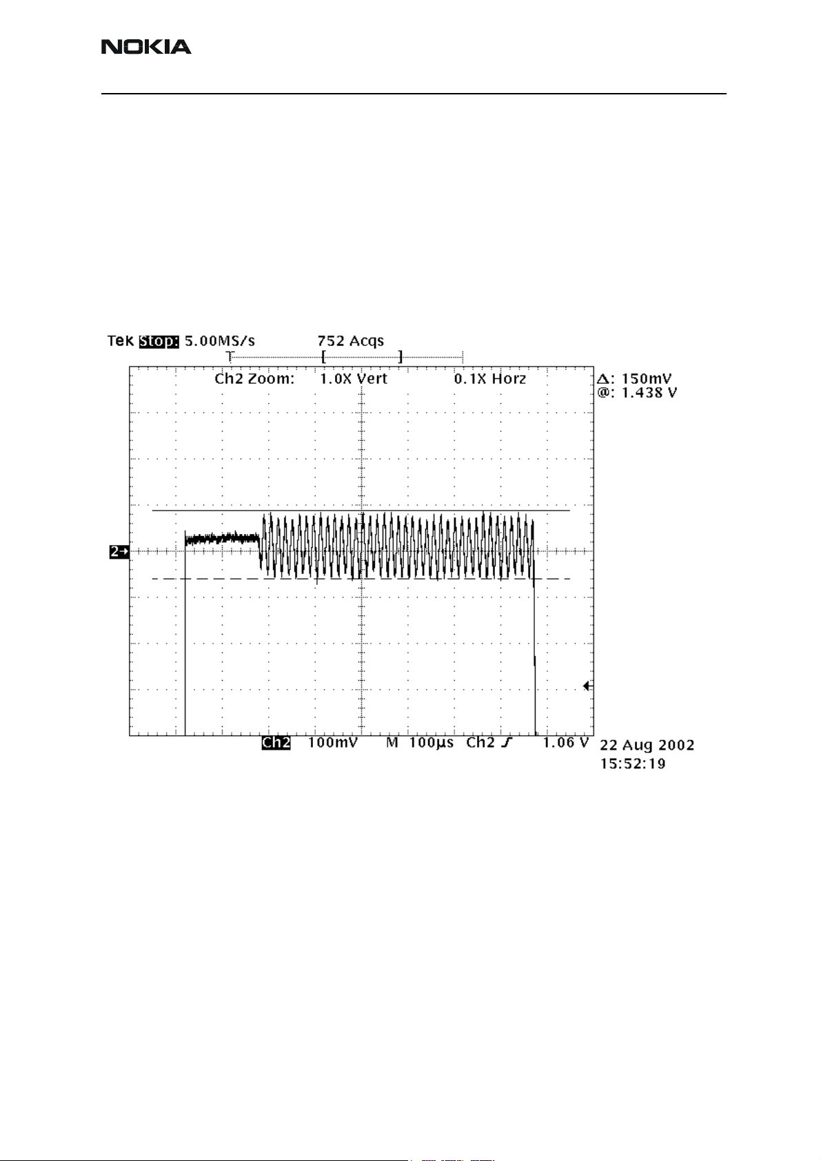
Measuring with an oscilloscope on "RXI" or "RXQ" following screens should be seen on a
working EGSM900 , GSM1800 or GSM1900 receiver:
Figure 8: RX I/Q signal ,burst mode, input level –90dBm.
Figure 8, “RX I/Q signal ,burst mode, input level –90dBm.,” on page 15: Receiver I or Q
burst mode signal (channel 37) measured from testpoint RXI or RXQ with 942.467 MHz
signal, input level –90dBm at RF-connector.
Correct signal amplitudes approximately:
• EGSM900~170mVpp
• GSM1800~140mVpp
• GSM1900~160mVpp
Signal part frequency 67.7kHz sine.
Issue 2 06/03 Copyright Nokia. All rights reserved.. Page 15
Page 16

NPM-6/6X Company confidential
Troubleshooting Instructions CCS Technical Documentation
DC level of signal part is 1.35V. DC level can variate about +/-100mV between I and Q
signals and between different bands as well.
Figure 9: GSM1900 RX I or Q signal (trace2), burst mode.
For GSM1900 receiver burst mode I or Q signal at ch 661 with input signal
1960.067MHz, level –90 dBm at RF-connector.
Trace2: With wider time scaling both monitoring and own RX bursts are seen, 1st burst
(shorter) is monitoring and 2nd burst (longer) is own RX burst.
Trace1: External LNA VCC supply voltage at burst mode, input level –90 dBm. Measured
from testpoint LNA_VCC.
Page 16 Copyright Nokia. All rights reserved. Issue 2 06/03
Page 17
Company confidential NPM-6/6X
CCS Technical Documentation Troubleshooting Instructions
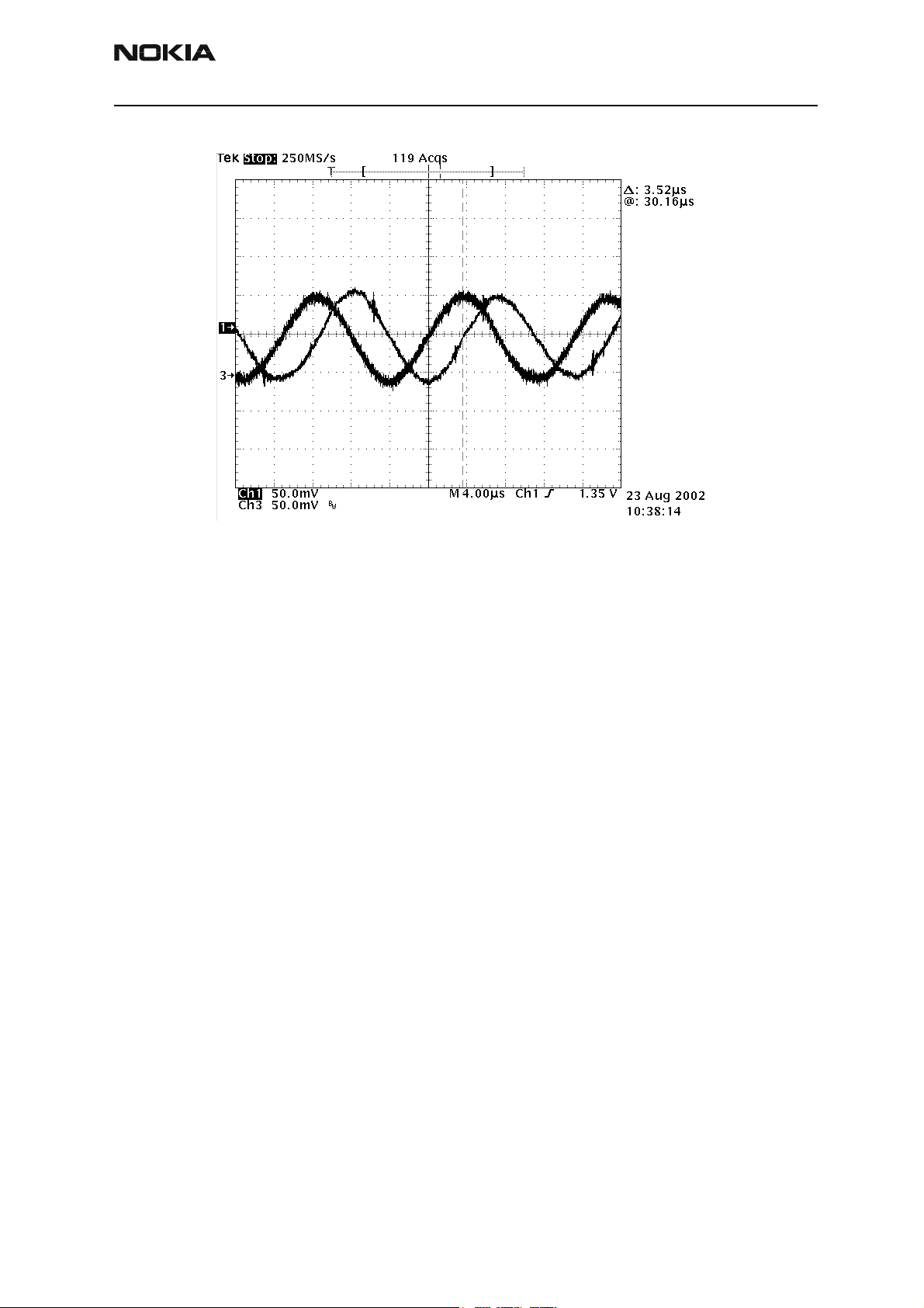
Figure 10: RX I&Q, phase difference 90 deg between signals.
Figure 10, “RX I&Q, phase difference 90 deg between signals.,” on page 17:
Detailed view of EGSM900 continuous mode RX I and Q signals measured from
testpoints RXI and RXQ simultaneously.
Used channel 37, input signal 942.467 MHz, level –90 dBm at antenna port, AGC setting
12.
Phase difference should be 90 degrees between RX I and Q signals at all bands.
Issue 2 06/03 Copyright Nokia. All rights reserved.. Page 17
Page 18

NPM-6/6X Company confidential
Troubleshooting Instructions CCS Technical Documentation
Troubleshooting diagram for EGSM900 receiver
Phone in “Continuous” mode, AGC setting “12”
Figure 11: EGSM900 receiver troubleshooting
Apply –90dBm
942.46771MHz signal
from generator to antenna connector
Yes
Oscilloscope at RX_I
Signal 700mVpp
DC offset 1.35V***
Frequency 67.7kHz
Yes
900RX chain
functional
No
Change generator level
to –50dBm
Spectrumanalyzer
Spectrumanalyzer
Antenna Switch
Antenna Switch
outputs, GSM900
outputs,EGSM900
–88 dBm
-88dBm
Yes
Spectrumanalyzer
HELGA inputs
GSM900
EGSM900 -89dBm
–89 dBm
Yes
Oscilloscope
VR1,3...6 2.7V
Check HELGA serial
interface
(burst mode)
NoYes
No
No
Spectrumanalyzer
Antenna Switch
input
–84 dBm
Yes
Oscilloscope
VANT_1...3 0V
Yes
Check Antenna
switch
Z800
Check L809
L810
Check Baseband
No
Check C831,
L811
Oscilloscope :
Check HELGA
serial interface
(burst mode)
Check HELGA
N500
All spectrumanalyzer reading
values are measured with
2.5 kohm passive probe (use
tweezers to connect the
probe ground to the nearest
PWB ground). Reading value
is represented without
+34 dB compensation.
* Spectrumanalyzer
reading with 1 kohm
passive probe (right value add +34 dB)
NoNo
Check Baseband
Yes
Spectrumanalyzer
4G VCO out
3769.6MHz
∼–30 dBm (*
Yes
Check HELGA
N500
No
Synthesiszer troubleshooting
* ** DC–level of RXI/RXQ in
continuous mode will decrease
slowly.
The original level can be restored by rewriting gain set.
Page 18 Copyright Nokia. All rights reserved. Issue 2 06/03
Page 19

Company confidential NPM-6/6X
N500
CCS Technical Documentation Troubleshooting Instructions
Troubleshooting diagram for GSM1800 receiver
Phone in “Continuous” mode, AGC setting “12
Figure 12: GSM1800 receiver troubleshooting
Apply –90dBm
1842.86771MHz signal
from generator to antenna connector
NoNoYesNoYes
Oscilloscope at RX_I
Signal 140mVpp
DC offset 1.35V ***
Frequency 67.7kHz
Yes
Change generator level
to –50dBm
Spectrumanalyzer
Antenna switch outputs,
1800 LNA out
–61 dBm
Spectrumanalyzer
Antenna Swithc input
-84 dBm
Check C831,
L811
GSM1800 RX chain
functional
Yes
Spectrumanalyzer
HELGA inputs
GSM 1800
–88 dBm
Yes
Oscilloscope
VR1,3...6 2.7V
Check HELGA serial
interface
(burst mode)
Yes
Spectrumanalyzer
4G VCO out
3769.6MHz
∼–30 dBm (*
Yes
Check HELGA
N500
No
No
No
Oscilloscope
VANT_1...3 0V
Check Antenna
Switch Z800
Check C838, C839,
L821. L 872,
C836, C837,
V801
Synthesiszer troubleshooting
Yes
Yes
Check Baseband
Oscilloscope
Check HELGA serial interface (burst
mode)
Yes
Check Helga
Check HELGA
N500
N600
All spectrumanalyzer reading
values are measured with 1
kohm passive probe (use
tweezers to connect the
probe ground to the nearest
PWB ground). Reading value
is represented without +26
dB compensation.
* Spectrumanalyzer
reading with 1 kohm
passive probe (right value add +26 dB)
* ** DC–level of RXI/RXQ in
continuous mode will decrease
slowly.
The original level can be restored by rewriting gain set.
NoNo
Check Baseband
Issue 2 06/03 Copyright Nokia. All rights reserved.. Page 19
Page 20

NPM-6/6X Company confidential
Z806
Troubleshooting Instructions CCS Technical Documentation
Troubleshooting diagram for GSM1900 receiver
Phone in “Continuous” mode, AGC setting “12
Figure 13: GSM1900 receiver troubleshooting
Apply –90dBm
1842.86771MHz signal
from generator to antenna connector
NoNoYesNoYes
Oscilloscope at
RX_I /RXQ
Signal 160mVpp
DC offset 1.35V ***
Frequency 67.7kHz
Change generator level
to –50dBm
Spectrumanalyzer
Antenna Switch output, GSM1900
–88 dBm
Spectrumanalyzer
Antenna Switch input
–84 dBm
Check C831,
L811
Yes
GSM1800 RX chain
functional
Spectrumanalyzer
HELGA inputs
GSM1900
–78 dBm
Oscilloscope
VR1,3...6 2.7V
Check HELGA serial
interface
(burst mode)
Yes
Spectrumanalyzer
4G VCO out
3685.6MHz
∼–30 dBm (*
Yes
Check HELGA
N500
Spectrumanalyzer
RX_SAW_out
Yes
–90 dBm
Oscilloscope
LNA_VCC 2.6V
LNA_P 0 V
Check V802,
C826, Z802,
C829, C8097,
C808
Check Baseband
Synthesiszer troubleshooting
Yes
Oscilloscope
VANT_3 2.7VV
VANT_1/2 0V
Check Antenna
switch Z800
Oscilloscope
VR1,3...6 2.7V
Check HELGA serial
interface
(burst mode)
Yes
Yes
Yes
Check HELGA
N500
Oscilloscope
Check HELGA serial interface (burst
mode)
Yes
Check HELGA
N500
Check Baseband
Check Baseband
All spectrumanalyzer reading
values are measured with 1
kohm passive probe (use
tweezers to connect the
probe ground to the nearest
PWB ground). Reading value
is represented without +26
dB compensation.
* Spectrumanalyzer
reading with 1 kohm
passive probe (right value add +26 dB)
* ** DC–level of RXI/RXQ in
continuous mode will decrease
slowly.
The original level can be restored by rewriting gain set.
NoNo
Check Baseband
Page 20 Copyright Nokia. All rights reserved. Issue 2 06/03
Page 21

Company confidential NPM-6/6X
CCS Technical Documentation Troubleshooting Instructions
Synthesizer
General instructions for synthesizer troubleshooting
Connect test jig to computer with DAU9S cable or to FPS-8 Flash Prommer with XCS-4
modular cable.
Make sure that you have PKD-1 dongle connected to computers parallel port.
Connect DC power supply or FPS-8 to module test jig with PCS-1 cable.
Set the DC supply voltage to 3.9V and set the jumper connector on test jig to "bypass"
position.
Set the phone module to test jig and start Phoenix service sofware
Initialize connection to phone. (use FBUS driver when using DAU9S and COMBOX driver
when using FPS-8)
Select product from the menu
File -> Choose product -> NPM-6
From toolbar set operating mode to "Local"
Activate RF controls window from the menu
Maintenance -> Testing -> RF Controls
From the RF controls window
- Select band "EGSM900", "GSM 1800" or "GSM1900" (Default = "EGSM900")
- Set Active unit to "Rx" (Default = "Rx")
- Set Operation mode to "Continuous" (Default = "Burst")
- Set Rx/Tx channel to 37 on EGSM900 band, 700 on GSM1800 band, 661 on GSM1900
band (Defaults)
Issue 2 06/03 Copyright Nokia. All rights reserved.. Page 21
Page 22

NPM-6/6X Company confidential
Check with RF
(
Troubleshooting Instructions CCS Technical Documentation
Synthesizer troubleshooting diagram
Figure 14:
Synthesizer
troubleshooting
*(When 2.5kOhm passive probe is used,
Yes
correct the measurement by +34 dB
Set with RF controls:
Active Unti = Rx
Operation mode = Continuous
Check with RF probe:
-4G VCO out signal
-4G VCO out signal
-3589.6 MHz (EGSM900)
- 3589.6 MHz (GSM900)
-3495.6 MHz (GSM1800)
-3495.6 MHz (GSM1800)
-3760 MHz
- 3760 MHz (GSM1900)
Level >-10dBm (*
VCO out signal level<-10dBm
Check output signal on
1 GHz span
Signal found on
incorrect frequency ?
probe:
GSM1900)
OK ?
No
No
Yes
Yes
Synthesizer
OK
Yes
Check with oscilloscope:
-4G VCO Vcc = 2.7V
No
Check balun
output levels and
solder joints
OK ?
No
Replace
faulty
component(s)
OK ?
No
Yes
Yes
Baseband
troubleshooting
Replace
VCO
Check with oscilloscope:
VCO control voltage
from VCO pin
0V ?
No
Check with oscilloscope:
VCO control voltage
from VCO pin
>4.0 V ?
Yes
Check balun
output levels and
solder joints
OK ?
Yes
Check VCO control
loop components
Yes
OK ?
Replace
VCO
No
Replace
faulty
component(s)
No
Page 22 Copyright Nokia. All rights reserved. Issue 2 06/03
Page 23

Company confidential NPM-6/6X
CCS Technical Documentation Troubleshooting Instructions
Pictures of synthesizer signals
Figure 15: 26MHz at G501 pin out
Figure 16:
Figure 17: 1800 TX, channel 512, burst mode
26MHz RFCLK at R420/C420
Issue 2 06/03 Copyright Nokia. All rights reserved.. Page 23
Page 24

NPM-6/6X Company confidential
/
Troubleshooting Instructions CCS Technical Documentation
Figure 18: 1900 RX, channel 810, continuous mode
Figure 19: VCO output, 1800 band, RX on, continuous output
REF 4 . 0 dBm ATT 10 dB
10dB
SPAN
1. 000 MHz
REFOFS
34. 0 dB
RBW
10 kHz
VBW
10 kHz
SWP
50 ms
CENTER 3. 685600 GHz SPAN 1. 000 MHz
Wed Aug 21 21: 23: 21 2002
A_vi ew B_bl ank
MARKER
3. 685604 GHz
-3.97 dBm
Page 24 Copyright Nokia. All rights reserved. Issue 2 06/03
Page 25

Company confidential NPM-6/6X
CCS Technical Documentation Troubleshooting Instructions
Baseband Troubleshooting
BB Measurement points
Figure 20: NPM-6 BB Measurement points, Top
GND
VBATT
BSI
BSI
FLSCSX
FLS2CSX
EXTRDX
EXTWRX
FLSCLK
UEMINT
DBUSCLK
SLEEPX
DBUSDA
PURX
DBUSEN1X
SLEEPCLK
MBUSTX
FBUSRX
CBUSDA
CBUSENX
MBUSRX
FBUSTX
CBUSCLK
CSX
VDD
SCLK
GND
SDA
VLED RESX
VLED+
VDDI
VCORE
VFLASH2
VFLASH1
VANA
VSIM
VIO
Issue 2 06/03 Copyright Nokia. All rights reserved.. Page 25
Page 26

NPM-6/6X Company confidential
Troubleshooting Instructions CCS Technical Documentation
Figure 21: NPM-6 BB Measurement points, Bottom
SIMRST
SIMCLK
SIMDATA
VPP
MBUS
GND
FBUSRX
FBUSTX
VSIM
CHARGE GND
CHARGE
Page 26 Copyright Nokia. All rights reserved. Issue 2 06/03
Page 27

Company confidential NPM-6/6X
CCS Technical Documentation Troubleshooting Instructions
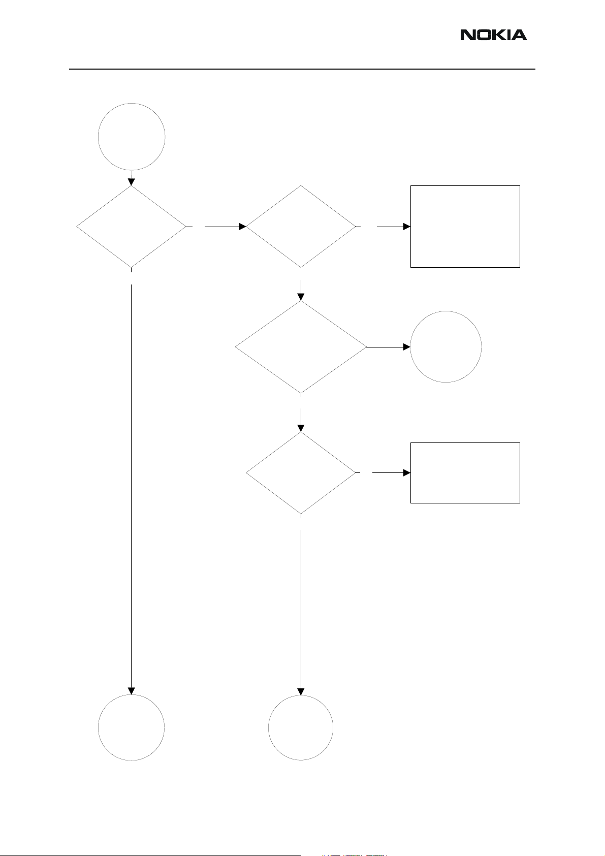
Troubleshooting diagrams
The following diagrams describe baseband troubleshooting.
Phone is dead
Phone current is
zero?
No
Phone current is
<50mA
No
Yes
Yes
Is phone flash
proramming OK
No
Yes
Check X100
Phone is
jammed
Flash faults
Check BSI line, X100,
Is phone in LOCAL
mode
Yes
Ok retest
No
C240,R203,
C100,R206
OK?
No
Yes
Change UEM
Repair
Issue 2 06/03 Copyright Nokia. All rights reserved.. Page 27
Page 28

NPM-6/6X Company confidential
Troubleshooting Instructions CCS Technical Documentation
Phone is jammed
Measure VIO, VCORE,
VFLASH1, VANA,
VR3 voltages.
Are they OK ?
Yes
Measure 32kHz
SleepClk from testpoint J404.
Is it OK ?
Yes
Measure 26MHz
RFClk from R420.
Is it OK ?
Check VBATT1-6
VIO,VCORE,VFLASH1,VANA,
No
No
No
VR3 lines.
Are they OK ?
Measure 32kHz
SleepClkfrom B200.
Is it OK ?
Measure 26MHz
RFCLK from C660.
Is it OK ?
Yes
Yes
No
No
No
Check X260-265,
C260-265, BSI/BTEMP
lines and VBATT lines
Check BSI/BTEMP
lines. If OK, change
UEM
Check B200,C209,
C210
Change UEM
Check C576,
R520,C540.
If OK change G501
Yes
Measure PURX signal
from testpoint J402.
Is it HIGH (1.8V) ?
Yes
Phone is
jammed
2
Yes
No
Check R420, C420.
If OK change N500
Change UEM
Page 28 Copyright Nokia. All rights reserved. Issue 2 06/03
Page 29

Company confidential NPM-6/6X
CCS Technical Documentation Troubleshooting Instructions
Phone is
jammed
2
Measure
Phone Shutdown
after 30s
Yes
watchdog signal
CBUSDA from J414.
Is it OK ?
No
Change
UPP
No
Measure
DBUSClk 1MHz signal
from testpoint J413.
Is it OK ?
Yes
Read phone info.
Is it OK ?
Yes
No
No
Yes
Retest
Measure FBUSRx
signal during phone info
read from testpoint J412.
Is it OK ?
Yes
No
Change
UEM
Measure FBUSTx
Change
UPP
Change
UEM
Retest
signal during phone info
read from testpoint J411.
Is it OK ?
Yes
No
Issue 2 06/03 Copyright Nokia. All rights reserved.. Page 29
Page 30

NPM-6/6X Company confidential
Troubleshooting Instructions CCS Technical Documentation
Flash faults
Phone doesn't set
FlashBus TxD line HIGH after the
startup?
No
Yes
Measure BSI pulse during
Flash programming.
Is it OK?
Yes
Measure FBusTx line during
Flash programming (TP 411)
Is it HIGH (1.8V)?
Yes
No
No
Check BSI
line, X100,
C240, R203,
C100, R206
Check
FBUSTx line. If
OK
Change UEM
Phone doesn't set
FlashBus TxD line LOW after the
line has been set HIGH
No
Flash faults
2
Yes
Change UPP
Page 30 Copyright Nokia. All rights reserved. Issue 2 06/03
Page 31

Company confidential NPM-6/6X
CCS Technical Documentation Troubleshooting Instructions
Flash faults
2
Wrong manufacturer
ID or Device ID
No
Phone is totally dead
No
Phone doesn't start
up or phone is jammed
Yes
Yes
Yes
Change Flash
Phone is dead
Phone is
jammed
No
Retest
Issue 2 06/03 Copyright Nokia. All rights reserved.. Page 31
Page 32

NPM-6/6X Company confidential
Troubleshooting Instructions CCS Technical Documentation
SIM card
faults
Insert SIM card faults
No
Yes
Set phone to
LOCAL mode.
Is it OK ?
Yes
Check X386
Measure VSIM
voltage from X386.
Is it 3V (1.8V)
Yes
No
No
Check BSI line, X100,
C240, R203, R206. If
OK change UEM
Check VSIM
line,X386,
C203,C370, L386. If
OK change R388. If
still wrong VSIM
change UEM
END
Check SIM
power up sequency.
Is it OK ?
Yes
Change UPP
No
Check SIM lines. If
OK change R388. If
still fail change UEM.
Page 32 Copyright Nokia. All rights reserved. Issue 2 06/03
Page 33

Company confidential NPM-6/6X
CCS Technical Documentation Troubleshooting Instructions
Display faults
Set phone to LOCAL mode. Set
VBATT to 4.2V. Start Display
test with Phoenix. Set display
ON
Are display light
(LED) turned on ?
Yes
No
Try to change
UI -module. Is it
working now ?
No
Check CALLED1
(N300/8 and DLIGHT
(V312/IN).Are
they HIGH ?
Yes
Measure
voltage over C304.
Is it typ. 8.6V ?
Yes
Yes
No
No
Board to boad
connector fault in
displaymodule or
faulty module.
Retest
Check lines of
CALLED1 and
DLIGHT. If lines are
OK change UEM
Check
C302,C303,L300,V30
0, R301, R302, R303,
R325, C304.
If OK change N300
Display faults
2
Measure
voltage between J303
and J302 .Is it
typ. 7.2V ?
Yes
Measure
voltage between X302,
pin 9. Is it
typ. 7.2V ?
No
No
Check V311, V312,
R311, R312.
Retest
Change X302.
Retest
Issue 2 06/03 Copyright Nokia. All rights reserved.. Page 33
Page 34

NPM-6/6X Company confidential
Troubleshooting Instructions CCS Technical Documentation
Display faults
Set phone to LOCAL mode. Set
VBATT to 4.2V. Start Display
test with Phoenix. Set display
ON
Are display light
(LED) turned on ?
Yes
No
Try to change
UI -module. Is it
working now ?
No
Check CALLED1
(N300/8 and DLIGHT
(V312/IN).Are
they HIGH ?
Yes
Measure
voltage over C304.
Is it typ. 8.6V ?
Yes
Yes
No
No
Board to boad
connector fault in
displaymodule or
faulty module.
Retest
Check lines of
CALLED1 and
DLIGHT. If lines are
OK change UEM
Check
C302,C303,L300,V30
0, R301, R302, R303,
R325, C304.
If OK change N300
Display faults
2
Measure
voltage between J303
and J302 .Is it
typ. 7.2V ?
Yes
Measure
voltage between X302,
pin 9. Is it
typ. 7.2V ?
No
No
Check V311, V312,
R311, R312.
Retest
Change X302.
Retest
Page 34 Copyright Nokia. All rights reserved. Issue 2 06/03
Page 35

Company confidential NPM-6/6X
CCS Technical Documentation Troubleshooting Instructions
Display faults
2
Board to boad
connector fault in
display module or faulty
module.
Retest
Does the display start ?
Try to change
No Yes
UI -module. Is it
working now ?
Yes
No
Measure VDDI/J301
(2.78V) and VDD/J300
(1.8V).Are
they OK ?
No
Check signals
RESX/J306,
SDA/J305,SCLK/J307,
CSX/J304.
Is it OK ?
Change X302
No
No
Check lines of
VFLASH1 and VIO. If
lines are OK change
UEM
Check lines of display
control. If OK change
UPP
END
Issue 2 06/03 Copyright Nokia. All rights reserved.. Page 35
Page 36

NPM-6/6X Company confidential
Troubleshooting Instructions CCS Technical Documentation
Audio faults
Check earpiece
contact springs from
Is earpiece
working ?
Yes
Try to change UI-
No Yes
module. Is it working
now ?
No
Change old UI -module back.Set
phone to LOCAL mode. Using
Phoenix Audiotest set EXT IN, HP
OUT, LOOP ON
old UI-module and
change earpiece and
foam to old
UI-module.
Retest.
Measure DC-
offset voltage from J310/ J311 and
GND pads. Is it ~1.38V ?
Yes
Measure
MICB2 voltage from
XMIC (L102 input).
Is it ~2.2V ?
Yes
No
No
Check L150, C155,
R151 and line.
If OK change UEM
Check L102, C116,
C150, R153, R154
and line.
If OK change UEM.
Audio faults
2
Earpiece
2
Page 36 Copyright Nokia. All rights reserved. Issue 2 06/03
Page 37

Company confidential NPM-6/6X
CCS Technical Documentation Troubleshooting Instructions
Audio faults
2
Is microphone
workin g ?
Yes
Try to change new
No
C-cover assembly. Is it
workin g now ?
No
Restore old C-cover. Set phone to
LOCAL mode. Using Phoenix
Audiotest set HP IN, EXT OUT,
LOOP ON
Measure MICB1-
voltage from J110 pad.
Is it ~1.38V ?
Yes
Check C151, R157,
C105,C154 and line.
If OK change UEM if still
fail change UPP
Yes
No
Check mic contact springs
from old C-Cover assembly.
If not OK change PopPort
assembly to old C-cover.
Retest.
Check L101,L108, C151,
C152, C153, R156,
R157, R176.
If OK change UEM
Audio faults
3
Issue 2 06/03 Copyright Nokia. All rights reserved.. Page 37
Page 38

NPM-6/6X Company confidential
Troubleshooting Instructions CCS Technical Documentation
Earpiece
2
Connect EXT audio
signal 1kHz(sine,
200mVpp) between
XMICP and XMICN
pads (X101, 11/12)
Measure sine
signal from earpiece
pads (J310,J311).
Is It ~880mVpp ?
Yes
Change UPP
Retest
No
Measure sine
signal from UEM
(R151,R152).
Is it ~130mVpp ?
No
Yes
Change UEM
Check R151,R152,
C155, L150 and lines.
Page 38 Copyright Nokia. All rights reserved. Issue 2 06/03
Page 39

Company confidential NPM-6/6X
CCS Technical Documentation Troubleshooting Instructions
Audio faults
3
IHF speaker or
IHF speaker working ?
No Yes
Try to change new
C-cover assembly
contact springs
fault.
Restest
Yes
END
Check C173,
C174, C175, L151, L152,
C170, C171, C172 and
IHF PA output lines.
Retest.
Yes
Restore old C-cover
Set phone to local mode with Phoenix.
Set buzzer ON, vol "9" and freq. to 1kHz.
Measure DC-
level between IHF
No
pads J156/J157 to
GND.
Is it ~1.8V ?
Yes
Measure AC-
level between IHF
pads (J156,J157).
Is it ~1.0Vrms ?
No
Check signal in C161.
Is it OK ?
Yes
Speaker
contact springs
Yes
No
faults.
Retest
Check C161,
C160,R163,
C169.
If OK then
change UEM
Check IHF PA
controls on J152,
J523,J154.
Is it OK ?
Change UPP
Change IHF PA
Yes
(N150)
Issue 2 06/03 Copyright Nokia. All rights reserved.. Page 39
Page 40
NPM-6/6X Company confidential
Troubleshooting Instructions CCS Technical Documentation
Keyboard
faults
Is the powerkey
working?
Yes
Measure voltage
No Yes
from S302 when powerkey is
from S302.
Is it HIGH?
Yes
Measure voltage
pressed.
Is it HIGH ?
Yes
Check S302.
Is it OK ?
No
Check R306,
C310, S302 and
POWERONX line.
If OK change UEM
Phone is
jammed
Change S302
Yes
Keyboard
faults
2
Phone is
dead
Page 40 Copyright Nokia. All rights reserved. Issue 2 06/03
Page 41

Company confidential NPM-6/6X
CCS Technical Documentation Troubleshooting Instructions
Keyboard
faults
2
Is UI-module
keymatrix working ?
Yes
No
Try to change
UI -module. Is it
working now ?
No
Measure ROW0-4
lines from X301.Are
they HIGH ?
Yes
Measure SLEEPX signal
from J403 when key
pressed.
Is it ~1.8V ?
Yes
Yes
No
No
UI connector pad fault in
UI-board or faulty
UI-module.
Retest
Check ROW0-4 lines,
X301. If OK change
Z300. If still fails change
UPP.
Check ROW0-4 lines,
X301. If OK change
Z300. If still fails change
UPP.
Keyboard
faults
3
When keypad is
pressed, the LED's are
turned on ?
Yes
Display
faults
No
Check ROW0-4 lines,
X301. If OK change
Z300. If still fails change
UPP.
Issue 2 06/03 Copyright Nokia. All rights reserved.. Page 41
Page 42

NPM-6/6X Company confidential
Troubleshooting Instructions CCS Technical Documentation
Keyboard
faults
3
Measure ROW0
Is volume up key
working ?
Yes
line from S300.
Is it ~1.8v ?
No
No
Yes
Check S300, S301
and lines. If OK
change Z300.
If still fail change UPP
Is volume down key
working ?
Yes
No
Measure COL1 from
S300 when key is pressed.
Is there 50us pulse ?
Yes
Measure ROW0
line from S301.
Is it ~1.8v ?
No
Measure COL4 from
S301 when key is pressed.
Is there 50us pulse ?
No
No
Yes
Check S300 and COL1
lines. If OK change
Z300.
If still fail change UPP
Change UPP
Check S300, S301 and
lines. If OK change
Z300.
If still fail change UPP
Check S301 and COL4
lines. If OK change
Z300.
If still fail change UPP
Yes
Keyboard
faults
4
Change UPP
Page 42 Copyright Nokia. All rights reserved. Issue 2 06/03
Page 43

Company confidential NPM-6/6X
CCS Technical Documentation Troubleshooting Instructions
Keyboard
faults
4
Set phone to LOCAL mode. Set
VBATT to 4.2V. Start Display
test with Phoenix. Set
"Keyboard lights" ON
Are keyboard
light (LED)
turned on ?
Yes
No
Try to change
UI -module. Is it
working now ?
No
Check CALLED1
(N300/8 and KLIGHT
(V314/IN).Are
they HIGH ?
Yes
Measure
voltage over C304.
Is it typ. 8.6V ?
Yes
Yes
No
No
UI-board pads fault or
faulty UI-board.
Retest
Check lines of
CALLED1 and
KLIGHT. If lines are
OK change UEM
Check
C302,C303,L300,V30
0, R301, R302, R303,
R325, C304.
If OK change N300
End
Measure
voltage between
V313/3. Is it
typ. 7.2V ?
Yes
Measure
voltage X301, pin 1.Is it
typ. 7.2V ?
No
No
Check V313, V314,
R313, R314
Check X301, R307
Issue 2 06/03 Copyright Nokia. All rights reserved.. Page 43
Page 44

NPM-6/6X Company confidential
Troubleshooting Instructions CCS Technical Documentation
Accesory if
faults
Check PopPort
connecor pin
Non-ACI
accessory detected and
working?
Insert mono
No No
headset
(HDB-4)
Check ACI line
trans.HIGH to LOW
(<0.6V) ?
Yes
Remove
headset
3(ACI) and line to
systemboard,
L106,R103, R109,
C103. If OK
change UEM.
Retest.
Check ACI line
trans. LOW to HIGH. Is
it OK ?
Yes
Audio OK ?
Check PopPort
connecor pin
3(ACI) and line to
No
No
systemboard,
L106,R103, R109,
C103. If OK
change UEM.
Check C107,
C108, L103, C114,
C119, R105, R106,
R164, R165, C157
Retest
Accessory if
fault
2
Audio fault
3
Page 44 Copyright Nokia. All rights reserved. Issue 2 06/03
Page 45

Company confidential NPM-6/6X
CCS Technical Documentation Troubleshooting Instructions
Accesory if
faults
Check PopPort
connecor pin
4(Vout)) and line to
systemboard, L107,
C102, C112, C101,
No
R111. If ok check
GENIO(0) signal on
N100/VEN. If it is
HIGH, change N100
ACI
accessory detected
and working?
No
Insert stereo
headset
(HDS-3)
Wait 5s
Measure Vout
levelPopPort connector
pin 4.
Is it ~2.8V
Yes
Reinsert
headset
Ref. picture
below. Is the start up
sequency like it ?
Yes
Audio OK ?
Check PopPort
connecor pin 3 (ACI)
and line to
No
No
systemboard,
L106,R103, R109,
C103. If OK change
UEM. Retest.
Check C107, C108,
C109, C117, L103,
L104, C113, C114,
C118, C119, R105,
R106, R107, R108,
R164,R165, R166,
R167, C157, C158
END
Audio fault
3
Issue 2 06/03 Copyright Nokia. All rights reserved.. Page 45
Page 46

NPM-6/6X Company confidential
Troubleshooting Instructions CCS Technical Documentation
Flashlight
faults
Set phone to LOCAL mode. Set
VBATT to 4.2V. Start Display
test with Phoenix.
Set "Flashlight" ON
Check CALLED1 (N300/8
and CALLED2 (V320/IN).Are
they HIGH ?
No
Check lines of
CALLED1 and
CALLED2. If lines are
OK change UEM
Are flashlight
(LED) turned on ?
Yes
Yes
Measure
voltage over C304.
Is it typ. 8.6V ?
Yes
Measure
voltage V317/3 .Is it
typ. 7.2V ?
Yes
No
No
Check
C302,C303,L300,V30
0, R301, R302, R303,
R325, C304.
If OK change N300
Check V320, V317,
R315, R316
Change V318,V319
Display faults
2
Page 46 Copyright Nokia. All rights reserved. Issue 2 06/03
Page 47

Company confidential NPM-6/6X
CCS Technical Documentation Troubleshooting Instructions
Self tests
If any self test is failed,
contact service
information will be
shown on display.
Set phone to LOCAL
mode
Use Phoenix BB Self
Tests. Run All
Self test show now what
test are failed.
Issue 2 06/03 Copyright Nokia. All rights reserved.. Page 47
Page 48

NPM-6/6X Company confidential
Troubleshooting Instructions CCS Technical Documentation
FM Radio troubleshooting
FM Radio component layout
Figure 22: Component placement
Page 48 Copyright Nokia. All rights reserved. Issue 2 06/03
Page 49

Company confidential NPM-6/6X
CCS Technical Documentation Troubleshooting Instructions
Figure 23: Trace layout.
Figure 24: FM radio block layout.
Components L103, L104, L105, C107, C108, C109, C117, C162, C163, R164, R165, R166
and R167 are not shown in the picture. Those components are placed in baseband section, near audio amplifier N150.
Issue 2 06/03 Copyright Nokia. All rights reserved.. Page 49
Page 50

NPM-6/6X Company confidential
Troubleshooting Instructions CCS Technical Documentation
FM Radio troubleshooting diagram
Notes to "FM Radio troubleshooting diagram"
Use 1MHz 1X probe when measuring Audio and clock signals with oscilloscope.
Use active RF probe when measuring frequencies with spectrum analyzer.
Note 1. RF test signal parameters:
- Amplitude, A, –67.0 dBm
- Carrier frequency, fc, 98,000 MHz
- Deviation, ∆f, 75 kHz
- Modulating frequency f
, 1,000 kHz (RF generator internal)
m
- FM stereo, mode R=L, pilot state ON
Page 50 Copyright Nokia. All rights reserved. Issue 2 06/03
Page 51

Company confidential NPM-6/6X
CCS Technical Documentation Troubleshooting Instructions
Figure 25: FM radio troubleshooting diagram
Set phone into local mode.
Start FM radio.
Does
the radio
start ?
YES
Connect RF test signal (note1)
Set radio channel to 98.0 MHz
Set radio volume to max.
Measure
Audio signal
from C162 and
C163.
Is it 1kHz
0.5–0.8Vp–p?
NO
Check
C107, C108,
C109, C117 ,
L105,C367,C378,
C379, L358.
Measure signal
from C162, C163
Is it 1kHz
0.5–0.8
Vp–p?
NO
Check
R359,R360,
V356, V357,
L356,L357,C357,
C358,C362.
Measure
signal from
J103, J104,
OK ?
NO
Change
N356.
Measure signal
from J103 and J104.
Is it
OK ?
Check
NO NO
YES
YES
YES
YES
C374, C375, R375,
R358 and measure
R372
32kHz clock signal
from J359,
retest starting.
Start OK ?
YES
Check
R164,
R165, R166,
R167, L103,L104
Measure
signal from J103
and J104.
Is it
0.015–0.3
Vp–p?
YES
NO
Measure
voltages from
pins 7 and 34,
is it –2.7 V ?
Retest starting.
Start OK now ?
OK, RETEST IN FLALI
Radio and RF generator
to 87.5 and 108.0 MHz.
Measure Audio from
C162 and C163.
Are both cases
1 kHz 0.5 – 0.8 Vp–p ?
V356, V357, L356,
L357, C357, C358, C362,
R359, R360.
T est again with
87.5 and 108.0 MHz.
Measure audio from
C162 and C163.
NO
87.5 and 108.0 MHz.
Measure audio from
C162 and C163.
NO
Set
Check
Both
OK?
Change
V356 and 357.
BOTH !
Retest with
Both OK ?
NO
NO
(pins 5,6,7,8,9,11,
12,13,17,33,34,35,
Check
:
N356 solders
36, 37.
,R364,
R368,
Start OK
R362
now ?
Start OK
now
YESYES
YES
YES
NO
Change
N356.
Radio start
OK
now?
NO
Baseband digital
fault (UPP)
YES
Audio
Amplifier
failure
(N150)
NO
Change
radio module TB4
OK, RETEST IN FLALI
E Nokia Corporation
Issue 2 06/03 Copyright Nokia. All rights reserved.. Page 51
Page 52

NPM-6/6X Company confidential
Troubleshooting Instructions CCS Technical Documentation
Diagrams of FM radio signals
Figure 26: Oscilloscope screen shot, Audio output
Signal 1: Audio output from PWB test points J103 and J104, with FM test signal, volume
100%.
Signal 2: Audio output from FM radio pins 22 and 23(same as in C162 and C163), with
FM test signal
Page 52 Copyright Nokia. All rights reserved. Issue 2 06/03
Page 53

Company confidential NPM-6/6X
CCS Technical Documentation Troubleshooting Instructions
Figure 27: FM radio clock from test point J359, 32 kHz frequency clock signal, when radio is on.
15:51:49 03 JUL 2002
#AT 0 dBREF -20.0 dBm
PEAK
LOG
10
dB/
WA SB
CORR
SC FS
CENTER 98.0000 MHz SPAN 300.0 kHz
#RES BW 10 kHz VBW 10 kHz #SWP 1.00 sec
MKR 97.9280 MHz
-71.03 dBm
SWEEP
CONT SGL
FREE RUN
VIDEO
LINE
EXTERNAL
SYNC CRD
TV TRIG
Figure 28: FM frequency from FM radio pin 37, the other end of L358, with FM test signal
10:46:24 03 JUL 2002
PEAK
LOG
10
dB/
#AT 10 dBREF .0 dBm
MKR
196.440 MHz
-9.40 dB
MEAS UNCAL
SWEEP
CONT SGL
FREE RUN
VIDEO
LINE
WA SB
CORR
SC FS
CENTER 196.450 MHz SPAN 1.000 MHz
#RES BW 10 kHz #VBW 10 kHz #SWP 20.0 msec
EXTERNAL
SYNC CRD
TV TRIG
Figure 29: VCO frequency from FM radio pins 3 and 4, the other ends of V356 and V357, with FM test signal
Issue 2 06/03 Copyright Nokia. All rights reserved.. Page 53
Page 54

NPM-6/6X Company confidential
Troubleshooting Instructions CCS Technical Documentation
Page 54 Copyright Nokia. All rights reserved. Issue 2 06/03
 Loading...