

Page 1

Customer Care Solutions
NPM-6/6X Series Transceivers
System Module and User
Interface
Issue 2 06/03 Nokia Corporation.
Page 2

NPM-6/6X
System Module and User Interface CCS Technical Documentation
This Page Intentionally Blank
Page 2 Nokia Corporation. Issue 2 06/03
Page 3

NPM-6/6X
CCS Technical Documentation System Module and User Interface
Table of Contents
Page No
Glossary of Terms.......................................................................................................... 5
Introduction.................................................................................................................... 8
Electrical Modules .......................................................................................................8
Interconnection Diagram .............................................................................................8
Temperature Conditions ..............................................................................................9
Humidity ......................................................................................................................9
System Module ............................................................................................................ 10
Baseband Module ......................................................................................................10
Block Diagram ........................................................................................................ 11
Technical Summary ...................................................................................................11
DC Characteristics................................................................................................... 12
External and Internal Signals and Connections .........................................................15
Digital Signals ......................................................................................................... 15
Analogue Signals..................................................................................................... 16
Keyboard (board-to-board) Connector.................................................................... 17
LCD Connector (Board to Board)........................................................................... 19
DC Connector.......................................................................................................... 20
Bottom Connector ................................................................................................... 20
SIM connector ......................................................................................................... 22
Internal Signals and Connections............................................................................ 23
Headset connector ................................................................................................... 24
Functional Description................................................................................................. 25
Modes of Operation ...................................................................................................25
No Supply................................................................................................................ 25
Back-up ................................................................................................................... 25
Acting Dead............................................................................................................. 25
Active ...................................................................................................................... 25
Sleep Mode.............................................................................................................. 26
Charging .................................................................................................................. 26
Battery ..................................................................................................................... 26
Power Up and Reset..................................................................................................... 28
A/D Channels............................................................................................................... 28
FM Radio ...................................................................................................................30
IR Module ............................................................................................................... 30
Backup Battery........................................................................................................ 30
SIM Interface........................................................................................................... 30
ACI .......................................................................................................................... 31
External Accessory Regulator................................................................................. 32
External Audio ...........................................................................................................32
internal Audio ............................................................................................................33
IHF Speaker & Stereo Audio Amplifier ................................................................. 33
Internal Microphone................................................................................................ 34
Internal Speaker....................................................................................................... 34
Memory Block ...........................................................................................................35
Security.................................................................................................................... 35
Clock distribution ......................................................................................................35
Audio Control.......................................................................................................... 36
Issue 2 06/03 Nokia Corporation. Page 3
Page 4

NPM-6/6X
System Module and User Interface CCS Technical Documentation
Accessory identification and Power Supply............................................................ 37
RF Module ................................................................................................................... 38
RF Frequency Plan .................................................................................................. 39
DC characteristics ......................................................................................................40
Regulators................................................................................................................ 40
Power Distribution .................................................................................................. 41
RF characteristics .......................................................................................................42
Transmitter characteristics ...................................................................................... 42
Receiver characteristics........................................................................................... 43
RF Block Diagram .................................................................................................. 43
RF Block Diagram NPM-6/6X ............................................................................... 44
Frequency synthesizers ........................................................................................... 45
Receiver................................................................................................................... 45
Transmitter .............................................................................................................. 46
Front End................................................................................................................. 47
Power Amplifier...................................................................................................... 48
RF ASIC Helga ....................................................................................................... 49
AFC function........................................................................................................... 49
Antenna .................................................................................................................. 49
Page 4 Nokia Corporation. Issue 2 06/03
Page 5

NPM-6/6X
CCS Technical Documentation System Module and User Interface
Glossary of Terms
ACCIf Accessory Interface block of MAD2WD1
ACI Accessory Control Interface
ADC Analog-Digital Converter
AEC Acoustic Echo Canceller
AFC Automatic Frequency Control
AEM Auxiliary Energy Management ASIC
AGC Automatic Gain Control
AIF Application Interface
ALWE Background noise suppressor
API Application Programming Interface
ARM Processor architecture
ASIC Application Specific Integrated Circuit
BB Baseband
BT Bluetooth
CBus Control Bus connecting UPP_WD2 with AEM and UEM
CCONT Power management IC for digital phones
CCI Camera Control Interface
CCP Compact Camera Port
CIS PCMCIA Card Information Structure
CMT Cellular Mobile Telephone (MCU and DSP)
CPU Central Processing Unit
CTSI Clocking Timing Sleep Interrupt
COBBA_GJP DCT3 RF-interface and audio codec ASIC with serial MAD interface
CSP Chip Scale Package
Issue 2 06/03 Nokia Corporation. Page 5
Page 6

NPM-6/6X
System Module and User Interface CCS Technical Documentation
DAC Digital-Analog Converter
DAI Digital Audio Interface
DB Dual band
DCT3 Digital Core Technology, 3rd generation
DCN Offset Cancellation control signal
DLL Dynamic Link Library
DRC Dynamic Range Controller
DSP Digital Signal Processor
EGSM Extended – GSM
EFR Enhanced Full Rate
EGPRS Enhanced General Packet Radio Service
EMC Electromagnetic compatibility
EMI Electromagnetic Interference
EXT RF External RF
FBUS Asynchronous Full Duplex Serial Bus
GPRS General Packet Radio Service
GSM Global System for Mobile communications
HS Half Rate Speech
HSCSD High Speed Circuit Switched Data
IC Integrated Circuit
I/O Input/Output
IrDA Infrared Association
LCD Liquid Crystal Display
LNA Low Noise Amplifier
Page 6 Nokia Corporation. Issue 2 06/03
Page 7

NPM-6/6X
CCS Technical Documentation System Module and User Interface
MBUS 1-wire half duplex serial bus
MCU Micro Controller Unit
MDI MCU-DSP Interface
MFI Modulator and Filter Interface
PA Transmit Power Amplifier
PC Personal Computer
PCM Pulse Code Modulation
PCM SIO Synchronous serial bus for PCM audio transferring
PCMCIA PC Memory Card International Association
PIFA Planar Inverted F-antenna
PWB Printed Wiring Board
RF Radio Frequency
SIM Subscriber Identity Module
SMART PCMCIA interface ASIC
UEM Universal Energy Management
UI User Interface
UPP Universal Phone Processor
VCXO Voltage Controlled Crystal Oscillator
VCTCXO Voltage Controlled Temperature Compensated Crystal Oscillator.
Issue 2 06/03 Nokia Corporation. Page 7
Page 8
NPM-6/6X
T
/
System Module and User Interface CCS Technical Documentation
Introduction
Electrical Modules
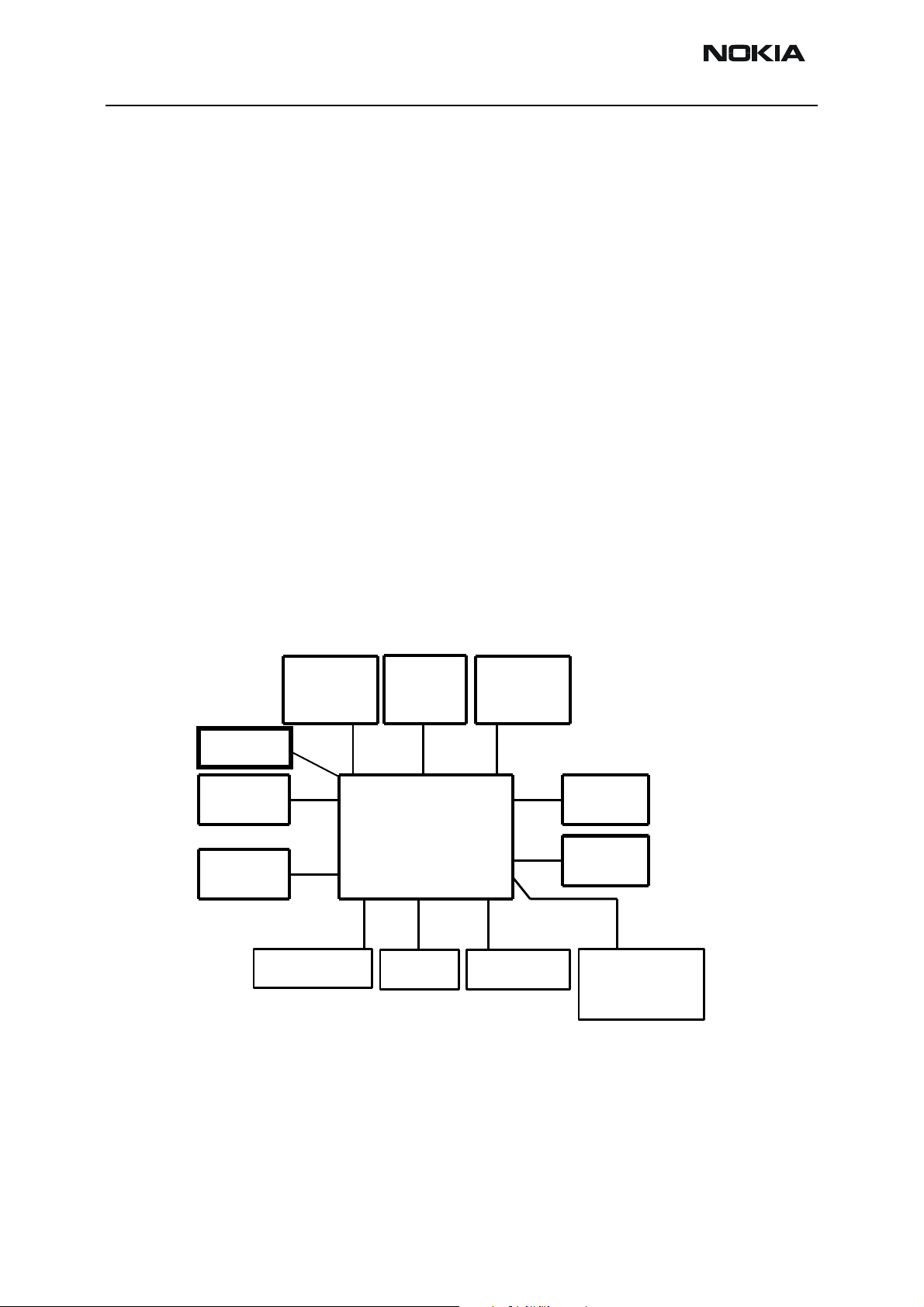
The system module AK4 consists of Radio Frequency (RF) and baseband (BB). User Interface (UI) contains display, keyboard, IR link, vibra, HF/HS connector and audio parts.
FM radio is located on the main PWB AK4.
The electrical part of the keyboard is located in separate UI PWB named KU4. KU4 is connected to radio PWB through spring connectors.
The Baseband blocks provide the MCU, DSP, external memory interface and digital control functions in the UPP ASIC. Power supply circuitry, charging, audio processing and RF
control hard ware are in the UEM ASIC.
The purpose of the RF block is to receive and demodulate the radio frequency signal from
the base station and to transmit a modulated RF signal to the base station.
The UI module is described in a dedicated section of the manual.
Interconnection Diagram
Keyboard
module
Flashlight
Antenna
Microphone
Figure 1: Interconnection diagram
Display
IHF
speaker
Radio
Module
NPM-6/6X
NHL-4
IR Link
Earpiece
BatterySIM
Charger
omahawk
Accessories
Page 8 Nokia Corporation. Issue 2 06/03
Page 9

NPM-6/6X
CCS Technical Documentation System Module and User Interface
Temperature Conditions
Specifications are met within range of -10...+55 deg. C ambient temperature
Storage temperature range -40...+70 deg. C
Humidity
Relative humidity range is 5... 95%.
This module is not protected against water. Condensated or splashed water might cause
malfunction momentary. Long term wetness will cause permanent damage.
Issue 2 06/03 Nokia Corporation. Page 9
Page 10

NPM-6/6X
System Module and User Interface CCS Technical Documentation
System Module
The System module (or Engine) consists of Baseband and RF sub-modules, each described
below.
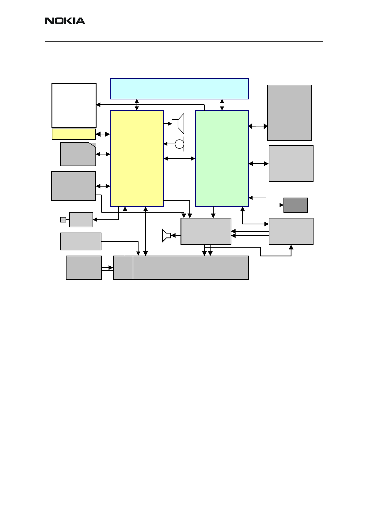
Baseband Module
Main functionality of the baseband is implemented into two ASICs: UPP (Universal Phone
Processor) and UEM (Universal Energy Management).
UPP ASIC provides the MCU, DSP, external memory interface and digital control functions.
UEM ASIC contains power supply circuitry, charging, audio processing and RF control
hardware.
The baseband architecture supports a power saving function called "sleep mode". This
sleep mode shuts off the VCTCXO, which is used as system clock source for both RF and
baseband. During the sleep mode the system runs from a 32 kHz crystal. The phone is
waken up by a timer running from this 32 kHz clock supply. The sleep time is determined
by net work parameters. Sleep mode is entered when both the MCU and the DSP are in
standby mode and the normal VCTCXO clock is switched off.
NPM-6/6X supports both three and two wire type of Nokia chargers. Three wire chargers
are treated like two wire ones. There is not separate PWM output for controlling charger
but it is connected to GND inside the bottom connector. Charging is controlled by UEM
ASIC (Universal Energy Management) and EM SW running in the UPP (Universal Phone
Processor).
BL-4C Li-ion rechargeable battery is used as main power source for NPM-6/6X. BL-4C
has a capacity of 720 mAh.
Page 10 Nokia Corporation. Issue 2 06/03
Page 11
NPM-6/6X
j
CCS Technical Documentation System Module and User Interface
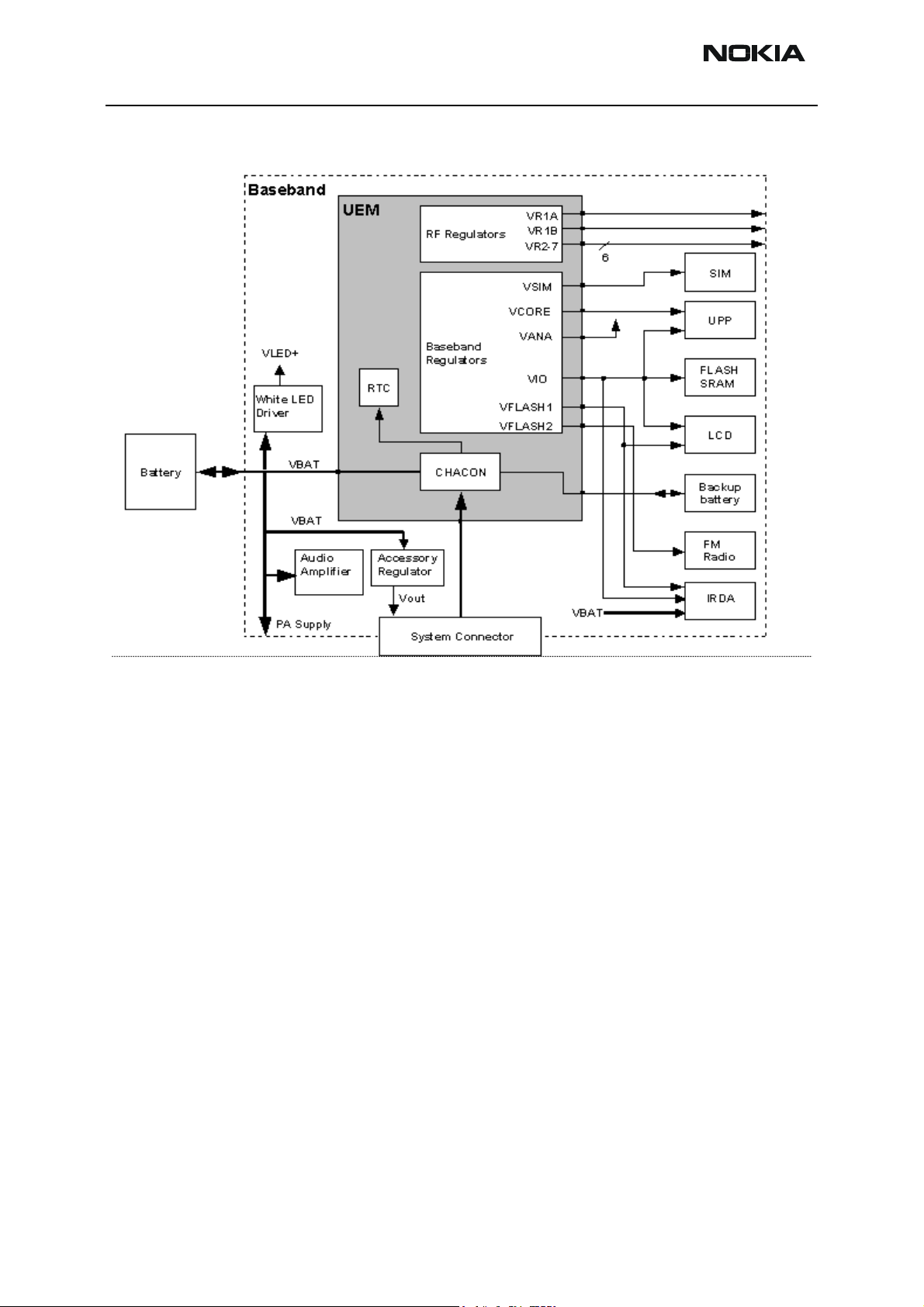
Block Diagram
Figure 2: Baseband block diagram
FLASH
64Mbit
(incl. EEPROM)
LCD
Passive colour STN
RF Interface
Flashlight
SIM
DCT-3
Battery
BL-4C
Vibra
Accessory
Regulator
Charger
SRAM
DC
ack
UEM
v4
IHF
System connector
Tomahawk
UPP8M
v2
Mo/St Amp
LM4855
Keyboard
FM radio
TEA5767
4Mbit
Keyboard
Illumination
1.8 V
IR
Technical Summary
Baseband of the NPM-6/6X is running from power rails 2.8V analog voltage and 1.8V I/O
voltage. UPP core voltages can be lowered down to 1.0V, 1.3V and 1.5V. UEM includes 6
linear LDO (low drop-out) regulator for baseband and 7 regulator for RF. It also includes
4 current sources for biasing purposes and internal usage. UEM also includes SIM interface which has supports both 1.8V and 3V SIM cards.
A real time clock function is integrated into the UEM, which utilizes the same 32kHz
clock supply as the sleep clock. A backup power supply is provided for the RTC-battery,
which keeps the real time clock running when the main battery is removed. The backup
power supply is a rechargeable surface mounted Li-Ion battery. The backup time with the
battery is 30 minutes minimum.
The interface between the baseband and the RF section is mainly handled by the UEM
ASIC. The UEM provides A/D and D/A conversion of the in-phase and quadrature receive
and transmit signal paths and also A/D and D/A conversions of received and transmitted
audio signals to and from the user interface. The UEM supplies the analog TXC and AFC
signals to RF section according to the UPP DSP digital control.
Issue 2 06/03 Nokia Corporation. Page 11
Page 12
NPM-6/6X
System Module and User Interface CCS Technical Documentation
Data transmission between the UEM and the UPP is implemented using two serial busses, DBUS for DSP and CBUS for MCU. There are also separate signals for PDM coded
audio. Digital speech processing is handled by the DSP inside UPP ASIC.
The UEM is a dual voltage circuit, the digital parts are running from the baseband supply
1.8V and the analog parts are running from the analog supply 2.78V also VBAT is directly
used.
The baseband supports both internal and external microphone inputs and speaker outputs. Input and output signal source selection and gain control is performed by the UEM
according to control messages from the UPP. Keypad tones, DTMF, and other audio tones
are generated and encoded by the UPP and transmitted to the UEM for decoding. An
external vibra alert control signals are generated by the UEM with separate PWM outputs.
NPM-6/6X has two serial control interfaces: FBUS and MBUS. FBUS can be accessed
through a test pad and the System Connector as described later. The MBUS can be
accessed through the production test pattern as described in section MBUS Interface.
Note! NPM-6 uses 64Mbit flash memory and external 4MBit SRAM memory. NPM-6X uses
COMBO memory including 64MBit flash memory and 4Mbit SRAM.
EMC shielding is implemented using a metallized plastic frame. On the other side, the
engine is shielded with PWB grounding.
DC Characteristics
Regulators and Supply Voltage Ranges
Absolute Maximum Ratings
Signal Note
Battery Voltage (Idle) -0.3V - 5.5V
Battery Voltage (Call) Max 4.8V
Charger Input Voltage -0.3V - 16V
Battery Voltage Range
Signal Min. Nom Max Note
VBAT 3.1V 3.7V 4.2V (charging
high limit voltage)
3.1V SW cut off
Page 12 Nokia Corporation. Issue 2 06/03
Page 13
NPM-6/6X
CCS Technical Documentation System Module and User Interface
BB Regulators
Signal Min. Nom Max Note
VANA 2.70V 2.78V 2.86V I
VFLASH1 2.70V 2.78V 2.86V I
VFLASH2 2.70V 2.78V 2.86V I
VSIM 1.745V
2.91V
1.8V
3.0V
1.855V
3.09V
VIO 1.72V 1.8V 1.88V I
VCORE 1.0V
1.235V
1.425V
1.710V
1.053V
1.3V
1.5V
1.8V
1.106V
1.365V
1.575V
1.890V
Current Sources
Signal Min. Nom Max Note
= 80mA
max
= 70mA
max
I
= 1.5mA
sleep
= 40mA
max
I
= 25mA
max
= 0.5mA
I
sleep
= 150mA
max
I
= 0.5mA
sleep
I
= 200mA
max
= 0.2mA
I
sleep
Default value 1.5V
IPA1 and IPA2 0mA - 5mA Programmable, +/-6%
IPA3 and IPA4 0.5mA 1mA 1.5mA V
V
IPA1,VIPA1
IPA1
= 0V - 2.7V
= 0V - 2.7V
Issue 2 06/03 Nokia Corporation. Page 13
Page 14
NPM-6/6X
System Module and User Interface CCS Technical Documentation
Power Distribution diagram
Page 14 Nokia Corporation. Issue 2 06/03
Page 15
NPM-6/6X
CCS Technical Documentation System Module and User Interface
External and Internal Signals and Connections
This section describes the external and internal electrical connection and interface levels
on the baseband. The electrical interface specifications are collected into tables that
covers a connector or a defined interface.
Digital Signals
AC and DC Characteristics of RF-BB digital signals
Signal name From To Parameter Input Characteristics
Min. Typ Max Unit
TXP UPP
GenIO 5
RFBusEna1X UPP Helga ”1” 1.38 1.88 V RFbus enable
RFBusData UPP the
Helga ”1” 1.38 1.88 V Power ampli-
”0” 0 0.4 V
Load Resistance 10 220 kohm
Load Capacitance 20 pF
Timing Accuracy 1/4 sym-
bol
”0” 0 0.4 V
Current 50 uA
Load resistance 10 220 kohm
Load capacitance 20 pF
”1” 1.38 1.88 V RFbus data;
Helga
Function
fier enable
read/write
”0” 0 0.4 V
Load resistance 10 220 kohm
Load capacitance 20 pF
Data frequency 10 MHz
RFBusClk UPP the
Helga
”1” 1.38 1.88 V RFbus clock
”0” 0 0.4 V
Load resistance 10 220 kohm
Load capacitance 20 pF
Data frequency 10 MHz
Issue 2 06/03 Nokia Corporation. Page 15
Page 16

NPM-6/6X
System Module and User Interface CCS Technical Documentation
RESET
UPP
GenIO 6
the
Helga
”1” 1.38 1.85 V Reset to the
Helga
”0” 0 0.4 V
Load capacitance 20 pF
Load resistance 10 220 kohm
Analogue Signals
Signal
name
VCTCXO VCTCXO UPP Frequency 13 26 MHz High stability
From To Parameter Min Typ Max Unit Function
Signal amplitude 0.2 1.32 Vpp
Input resistance 10 kohm
Input capacitance
Harmonic content
10 pF
-8 dBc
clock signal for
the logic circuits,
AC coupled. Distorted sinewave
eg. sawtooth.
Clear signal window (no glitch)
Duty cycle 40 60 %
VCTCXOGnd VCTCXO UPP DC level 0 V Ground for refer-
RXI/RXQ Helga UEM Voltage swing
(static)
DC level 1.3 1.35 1.4 V
Input impedance 500 kohm
TXIP / TXIN UEM the
Helga
Differential voltage swing (static)
DC level 1.17 1.20 1.23 V
Source impedance
200 mVpp
ence clock
1.35 1.4 1.45 Vpp Received demodulated I- and Qsignals
2.15 2.2 2.25 Vpp Programmable
voltage swing.
Programmable
common mode
200 ohm
voltage.
Between TXIPTXIN
Page 16 Nokia Corporation. Issue 2 06/03
Page 17

NPM-6/6X
CCS Technical Documentation System Module and User Interface
TXQP / TXQN UEM Helga Same as TXIP / TXIN
AFC UEM VCTCXO Voltage Min.
Max
Source impedance
Load
resistance
capacitance
Resolution 11 bits
TXC UEM Helga Voltage Min.
Max
Source impedance
Load
resistance
capacitance
Resolution 10 bits
0.0
2.4
200 ohm
1
2.4
5
0.1
2.55
100
0.1 V Transmitter power
200 ohm
15
V Automatic fre-
kohm
nF
kohm
pF
quency control
svoltage for the
VCTCXO
level and ramping
control
RFTemp Helga UEM Voltage at -20
deg.C
Voltage at +25
deg.C
Voltage at +60
deg.C
1,57
1,7
1,79
V Temperature sen-
sor of the RF.
Keyboard (board-to-board) Connector
Pin Signal Min. Nom Max Condition Note
1 VLED+ 7.2 V 0V
7.7 V
2 VLED-
(GND)
3 VLED+ 7.2 V 0V
4 KEYB2 0.293V 0.309V 0.324V 25°C Ambient temp. sensor on KU4
0.2 V 0V 0.35 V LED off
7.7 V
8.4 V LED off
LED on
LED on
8.4V LED off
LED on
Supply Voltage for Keyboard
LEDs
LED Katode Voltage
Supply Voltage for Keyboard
LEDs
5 Not connected
6 GND 0V
Issue 2 06/03 Nokia Corporation. Page 17
Page 18

NPM-6/6X
System Module and User Interface CCS Technical Documentation
7 ROW (4) 0.7xVIO
0
8 ROW(3) 0.7xVIO
0
9 COL(2) 0.7xVIO
0
10 ROW(1) 0.7xVIO
0
11 COL(1) 0.7xVIO
0
12 ROW (0) 0.7xVIO
0
13 ROW (1) 0.7xVIO VIO
14 COL (3) 0.7xVIO VIO
15 COL(4) 0.7xVIO
0
16 GND 0V
1.8 V
0.3xVIO
VIO
0.3xVIO
VIO
0.3xVIO
VIO
0.3xVIO
VIO
0.3xVIO
VIO
0.3xVIO
0.3xVIO
0.3xVIO
VIO
0.3xVIO
High
Low
High
Low
High
Low
High
Low
High
Low
High
Low
High
Low
High
Low
High
Low
Keyboard matrix row 4
Keyboard matrix row 3
Keyboard matrix column 2
Keyboard matrix row 1
Keyboard matrix column 1
Keyboard matrix row 0
Keyboard matrix row 1
Keyboard matrix column 3
Keyboard matrix column 4
Note: VIO is specified in Table 3 ‘Baseband Regulators’
Page 18 Nokia Corporation. Issue 2 06/03
Page 19

NPM-6/6X
CCS Technical Documentation System Module and User Interface
LCD Connector (Board to Board)
Pin Signal Min Nom Max Condition Note
1 VDDI 1.72V 1.8V 1.88V Logic voltage supply
Connected to VIO
2 RESX 0.7*VDDI
0
1us t
3 SDA 0.7*VDDI
0
100ns t
100ns t
4 SCLK 0.7*VDDI
0
250ns t
100ns t
100ns t
5 CSX 0.7*VDDI
0
60ns t
VDDI
0.3*VDDI
VDDI
0.3*VDDI
VDDI
0.3*VDDI
6.5MHz
VDDI
0.3*VDDI
Logic ’1’
Logic ’0’
rw
Logic ’1’
Logic ’0’
sds
sdh
Logic ’1’
Logic ’0’
Max frequency
scyc
shw
slw
Logic ’1’
Logic ’0’
css
Reset
Active low
Reset active
Serial data
Data setup time
Data hold time
Serial clock input
Clock cycle
Clock high
Clock low
Chip select
Active low
CXS low before SCLK rising
edge
100ns t
csh
CXS low after SCLK rising
edge
6 VDD 2.70V 2.78V 2.86V Supply Voltage.
Connected to VFLASH1
7 NC Not Connected
8 GND 0V Ground
9 VLED-
0V Return current
(GND)
10 VLED
Display
7.2V
0V
7.7V
8.4V
LED off
LED on
Supply Voltage for LEDs
Issue 2 06/03 Nokia Corporation. Page 19
Page 20

NPM-6/6X
System Module and User Interface CCS Technical Documentation
DC Connector
Pin Signal Min. Nom Max Condition Note
1 VCHAR 11 . 1V
7.0 V
RMS
2 CHGND 0 Charger ground
8.4 V
peak
RMS
16.9 V
7.9 V
1.0 A
9.2 V
850 mA
peak
RMS
peak
RMS
Standard
charger
Fast charger
Charger positive
input
Bottom Connector
Bottom connector is of type Pop-Port (TM)
Figure 3: Bottom connector pinout
1
Contacts, 14 pcs
14
Locking holes for
accessories, 2 pcs
Bottom connector pins and signals:
Pin/Signal
name
1 / Charge V Charge DC 0-9 V / 0.85 A
2 / GND Charge GND - 0.85 A 100 mOhm
3 / ACI ACI 1 kbit/s Digital 0 /
4 / Vout DC out DC 2.78V 70mA
Signal
description
Spectral range
Voltage /
Current levels
(PWB +
conn.)
2.5V-2.78V
2.5V 90mA
Max or
nominal
serial
impedance
47 Ohm
(lowpass
50kHz)
500 mOhm
(PWB +
conn.)
Note
Insertion &
removal
detection
200mW
Page 20 Nokia Corporation. Issue 2 06/03
Page 21

NPM-6/6X
CCS Technical Documentation System Module and User Interface
5 / USB Vbus DC in DC 4.375-5.25V USB spec.
6 / USB D+ /
FBUS RX
7 / USB D- /
FBUS TX
8 / USB data
GND
9 / XMIC N Audio in 300 - 8kHz 1Vpp & 2.5V-
10 / XMIC P Audio in 300 - 8kHz 1Vpp & 2.5V-
11 / HSEAR N Audio out 20 - 20kHz 1Vpp 10 Ohm
12 / HSEAR P Audio out 20 - 20kHz 1Vpp 10 Ohm
13 / HSEAR R N Audio out 20 - 20kHz 1Vpp 10 Ohm Not conn. In
14 / HSEAR R P Audio out 20 - 20kHz 1Vpp 10 Ohm Not conn. In
Data GND - ferrite USB spec.
FBUS nominal
115 k , fa s t F BUS
1.295M, USB
12M
FBUS nominal
115 k , fa s t F BUS
1.295M, USB
12M
USB 0-3.3V
Fbus 0 / 2.5V-
2.78V
FBUS RX
USB 0-3.3V
Fbus 0 / 2.5V-
2.78V
2.78VDC
2.78VDC
33 Ohm USB spec.
33 Ohm USB spec.
mono
mono
Table 1: Board to board connector pinlist (for PopPort Assembly)
Pin Symbol Pop-Port pin Note Max
1 Shield GND
2 Charge 1 In current from charger 16V/2A
3 Charge GND 2 Return current 16V/2A
4 Shield GND
5 ACI 3 Digital input 2.8V
6 Vout 4 Voltage output 2.8V/0.5A
7 USB Vbus 5 Voltage supply input 5V/1A
8 USB D+ /Fbus RX 6 Digital input 2.8V
9 USB D- /Fbus TX 7 Digital output 2.8V
10 Data GND 8 Return current 1.5A
11 XMIC N 9 Audio input
12 XMIC P 10 Audio input
13 XEAR N 11 Audio output
Issue 2 06/03 Nokia Corporation. Page 21
Page 22

NPM-6/6X
System Module and User Interface CCS Technical Documentation
14 XEAR P 12 Audio output
15 XEAR LN 13 Audio output
16 XEAR LP 14 Audio output
17 Shield GND
SIM connector
Pin Name Parameter Min. Typ Max Unit Notes
1 VSIM 1.8V SIM Card 1.6 1.8 1.9 V Supply voltage
3V SIM Card 2.8 3.0 3.2 V
2 SIMRST 1.8V SIM Card 0.9xVSIM
0
3V SIM Card 0.9xVSIM
0
3 SIMCLK Frequency 3.25 MHz SIM clock
Trise/Tfall 50 ns
1.8V Voh
1.8V Vol
3V Voh
3V Vol
4 DATA 1.8V Voh
1.8V Vol
3V Voh
3V Vol
1.8V Vih
1.8V Vil
3V Vil
3V Vil
0.9xVSIM
0
0.9xVSIM
0
0.9xVSIM
0
0.9xVSIM
0
0.7xVSIM
0
0.7xVSIM
0
VSIM
0.15xVSIM
VSIM
0.15xVSIM
VSIM V
VSIM V
VSIM
0.15xVSIM
VSIM
0.15xVSIM
VSIM
0.15xVSIM
VSIM
0.15xVSIM
V SIM reset (output)
V
V SIM data (output)
V SIM data (input)
Trise/Tfall max 1us
5 NC Not connected
6 GND GND 0 0 V Ground
Page 22 Nokia Corporation. Issue 2 06/03
Page 23

NPM-6/6X
CCS Technical Documentation System Module and User Interface
Internal Signals and Connections
FM Radio Interface
BB Signal
FM Radio
Signal
Min. Nom Max Condition Note
VFLASH2 Vcc1 2.7V 2.78V 2.86V max. Icc1 19mA
Vcc2 2.7V 2.78V 2.86V max. Icc2 800uA
VDD 2.7V 2.78V 2.86V max. IDD 3mA
GenIO(3) FMClk 1.4V
0
1.8V 1.88V
0.4V
High
Low
Reference clock for
FM radio module
75581 kHz Frequency In GSM
30ppm Stability
GenIO(8) FMWrEn 1.4V
0V
20µst
2 µs
1.8V 1.88V
0.4V
t
rise
High
Low
wd
rise / fall time
FMWrEn high before
rising edge of FMC-
trlClk (write opera
tion)
GenIO(11) FMCtrlClk 1.4V
0
1.8V 1.88V
0.4V
High
Low
max. 300kHz
50 ms t
GenIO(12) FMCtrlDa 1.4V
0
10 µst
1.5 µst
GenIO(27) FMTuneX 1.4V
0
1 µst
1.8V 1.88V
0.4V
14us t
1.8V 1.88V
0.4V
/ t
r
start
High
Low
da
shift
hold
High
Low
f
rise / fall time
FMCtrlClk delay after
switching on the
VFLASH2 (oscillator
running)
Bidirectional
shift register available after "search
ready"
data available after
FMCtrlClk rising
edge (read operation)
FMCtrlDa stable
after FMCtrlClk rising edge (write opera
tion)
from FM module to
UPP (FMCtrlClk = '1')
Issue 2 06/03 Nokia Corporation. Page 23
Page 24

NPM-6/6X
System Module and User Interface CCS Technical Documentation
MIC3P FMAudio 228mV
326mV
pp
460mV
pp
pp
50dB S/N
2% Harmonic
distortion
Internal microphone
Signal Min. Nom Max Condition Note
MICP 200mV
AC 2.2kΩ to
pp
2.0 V 2.1 V 2.25 V DC
MICN 2.0V 2.1V 2.25V DC
Internal speaker
Signal Min. Nom Max Condition Note
EARP 0.75V 0.8V 2.0 V
0.85V
EARN 0.75V 0.8V 2.0 V
0.85V
pp
pp
AC
DC
AC
DC
MIC1B
Differential output
(V
= 4.0 Vpp)
diff
Headset connector
Pin Signal Min. Nom Max Condition Note
5XMICP 1V
pp
100 mV
pp
2.0 V 2.1 V 2.25 V DC
3XMICN 1V
pp
100 mV
pp
4 XEARN 0.75V 0.8V 0.85V DC
1V
pp
7 XEARP 0.75V 0.8V 0.85V DC
1V
pp
5 HookInt 0V 2.86V
(VFLASH1)
6 HeadInt 0V 2.86V
(VANA)
G = 0dB 1kΩ to MIC2B
G = 20dB
G = 0 dB 1kΩ to GND
G = 20dB
AC
AC
Connected to
UEM AD-converter
Accessory detection
Page 24 Nokia Corporation. Issue 2 06/03
Page 25

NPM-6/6X
CCS Technical Documentation System Module and User Interface
Functional Description
Modes of Operation
AK4 baseband has six different functional modes:
- No supply
- Back-up
-Acting Dead
-Active
- Sleep
- Charging
No Supply
In NO_SUPPLY mode, the phone has no supply voltage. This mode is due to disconnection
of main battery and backup battery or low battery voltage level in both of the batteries.
Phone is exiting from NO_SUPPLY mode when sufficient battery voltage level is detected.
Battery voltage can rise either by connecting a new battery with VBAT > V
connecting charger and charging the battery above V
Back-up
In BACK_UP mode the backup battery has sufficient charge but the main battery can be
disconnected or empty (VBAT < V
VRTC regulator is disabled in BACK_UP mode. VRTC output is supplied without regulation
from backup battery (VBACK). All the other regulators are disabled in BACK_UP mode.
Acting Dead
If the phone is off when the charger is connected, the phone is powered on but enters a
state called ”Acting Dead”. To the user, the phone acts as if it was switched off. A battery
charging alert is given and/or a battery charging indication on the display is shown to
acknowledge the user that the battery is being charged.
and VBACK > VBU
MSTR
MSTR+
COFF
or by
MSTR+
.
).
Active
In the Active mode the phone is in normal operation, scanning for channels, listening to
a base station, transmitting and processing information. There are several sub-states in
the active mode depending on if the phone is in burst reception, burst transmission, if
DSP is working etc.
One of the sub-states of the active mode is FM radio on state. In that case, Audio Amplifier and FM radio are powered on. FM radio circuitry is controlled by the MCU and
Issue 2 06/03 Nokia Corporation. Page 25
Page 26

NPM-6/6X
System Module and User Interface CCS Technical Documentation
13MHz-reference clock is generated in the UPP. VFLASH2 regulator is operating.
In Active mode the RF regulators are controlled by SW writing into EM’s registers wanted
settings: VR1A can be enabled or disabled. VR2 can be enabled or disabled and its output
voltage can be programmed to be 2.78V or 3.3V. VR4 -VR7 can be enabled, disabled, or
forced into low quiescent current mode. VR3 is always enabled in Active mode.
Sleep Mode
Sleep mode is entered when both MCU and DSP are in stand–by mode. Sleep is controlled by both processors. When SLEEPX low signal is detected UEM enters SLEEP mode.
VCORE, VIO and VFLASH1 regulators are put into low quiescent current mode. All the RF
regulators are disabled in SLEEP. When SLEEPX=1 detected UEM enters ACTIVE mode and
all functions are activated.
The sleep mode is exited either by the expiration of a sleep clock counter in the UEM or
by some external interrupt, generated by a charger connection, key press, headset connection etc.
In sleep mode VCTCXOr is shut down and 32 kHz sleep clock oscillator is used as reference clock for the baseband.
Charging
Charging can be performed in any operating mode.
NPM-6/6X supports the standard NMP charger interface.
Supported chargers are ACP-7, ACP-8, ACP-9, ACP-12, LCH-8 and LCH-9.
Charging is controlled by the UEM ASIC and external components are needed for EMC,
reverse polarity and transient protection of the input to the baseband module. The
charger connection is through the system connector interface. The NPM-6/6X baseband
is designed to support DCT3 chargers from an electrical point of view. Both 2- and 3-wire
type chargers are supported.
The operation of the charging circuit has been specified in such a way as to limit the
power dissipation across the charge switch and to ensure safe operation in all modes.
Battery
720 mAh Li-ion battery pack BL-4C is used in NPM-6/6X.
Nominal discharge cut-off voltage 3.1V
Nominal battery voltage 3.7V
Nominal charging voltage 4.2V
Maximum charger output current 850 mA
Minimum charger output current 200 mA
Page 26 Nokia Corporation. Issue 2 06/03
Page 27

NPM-6/6X
CCS Technical Documentation System Module and User Interface
Pin numbering of battery pack
Signal name Pin number Function
VBAT 1 Positive battery terminal
BSI 2 Battery capacity measurement (fixed resistor inside the battery
pack)
GND 3 Ground/negative/common battery terminal
BL-4C battery pack pin order
Figure 4: Battery Pack Contents
4(GND)
3(BTEMP)
2(BSI)
1 (+)
Issue 2 06/03 Nokia Corporation. Page 27
Page 28

NPM-6/6X
System Module and User Interface CCS Technical Documentation
Power Up and Reset
Power up and reset is controlled by the UEM ASIC. NPM-6/6X baseband can be powered
up in following ways:
Press power button which means grounding the PWRONX pin on UEM
Connect the charger to the charger input
Supply battery voltage to the battery pin.
RTC Alarm, the RTC has been programmed to give an alarm
After receiving one of the above signals, the UEM counts a 20ms delay and then enters
its reset mode. The watchdog starts up, and if the battery voltage is greater than Vcoff+
a 200ms delay is started to allow references etc. to settle. After this delay elapses the
VFLASH1 regulator is enabled.
500us later VR3, VANA, VIO and VCORE are enabled. Finally the PURX line is held low for
20 ms. This reset, PURX, is fed to the baseband ASIC UPP, resets are generated for the
DSP and the MCU. During this reset phase the UEM forces the VCXO regulator on regardless of the status of the sleep control input signal to the UEM. The sleep signal from the
ASIC is used to reset the flash during power up and to put the flash in power down during sleep. All baseband regulators are switched on at the UEM power on except for the
SIM regulator that is controlled by the MCU. The UEM internal watchdog is running during the UEM reset state, with the longest watchdog time selected. If the watchdog
expires, the UEM returns to power off state. The UEM watchdog is internally acknowledged at the rising edge of the PURX signal in order to always give the same watchdog
response time to the MCU.
A/D Channels
The UEM contains the following A/D converter channels that are used for several measurement purpose. The general slow A/D converter is a 10 bit converter using the UEM
interface clock for the conversion. An interrupt will be given at the end of the measurement.
The UEM’s 11-channel analog to digital converter is used to monitor charging functions,
battery functions, user interface and RF functions.
When the conversion is started the converter input is selected. Then the signal processing block creates a data with MSB set to’1’ and others to’0’. In the D/A converter this
data controls the switches which connect the input reference voltage (VrefADC) to the
resistor network. The generated output voltage is compared with the input voltage under
measurement and if the latter is greater, MSB remains’1’ else it is set’0’. The following
step is to test the next bit and the next…until LSB is reached. The result is then stored to
ADCR register for UPP to read.
The monitored battery functions are battery voltage (VBATADC), battery type (BSI) and
Page 28 Nokia Corporation. Issue 2 06/03
Page 29

NPM-6/6X
CCS Technical Documentation System Module and User Interface
battery temperature (BTEMP) indication.
The battery type is recognized through a resistive voltage divider. In phone there is a
100kΩ pull up resistor in the BSI line and the battery has a pull down resistor in the
same line. Depending on the battery type the pull down resistor value is changed. The
battery temperature is measured equivalently except that the systemboard has an NTC
pull down resistor in the BTEMP line.
KEYB1&2 inputs are used for ambient temperature sensor. These inputs are also routed
internally to the miscellaneous block.
The monitored RF function is PATEMP detection. PATEMP input is used to measure temperature of the RFIC, the Helga.
Issue 2 06/03 Nokia Corporation. Page 29
Page 30

NPM-6/6X
System Module and User Interface CCS Technical Documentation
FM Radio
FM radio circuitry is implemented using the integrated radio IC, TEA5767. Only a few
external components like filters, discriminator and capacitors are needed.
TEA5767 is an integrated AM/FM stereo radio circuit including digital tuning and control
functions. NPM-6/6X radio is implemented as FM stereo receiver.
Figure 5: FM radio
HSE ARN
HSE ARP
HSE ARR N
HSE ARR P
IR Module
The IR interface when using transceiver with 1.8V I/O is designed into the UPP. The IR
link supports speeds from 9600 bit/s to 1.152 MBit/s up to distance of 80 cm. Transmission over the IR if half-duplex.
UEM
Audio Amp.
Antenna
connect i on
Vf l a s h 2
Mi c3 P
Li n
Ri n
VDI G
VCC
VCCVCO
VAFL
VAFR
FM Radi o
RF
IN
1
RFI
N2
Xt a l 2
SDA
SCL
W/R
UPP 8 Mv2.X
FMCl k
Genio( 3)
FMCt r l Da
Genio( 12)
FMCtr lCl k
Genio( 11)
FMWrEn
Genio( 8)
Backup Battery
Backup battery is used in case when main battery is either removed or discharged.
Backup battery is used for keeping real-time clock running for minimum of 30 minutes.
Rechargeable backup battery is connected between UEM VBACK and GND. In UEM
backup battery charging high limit is set to 3.2V. The cut–off limit voltage (V BUCoff–)
for backup battery is 2.0V. Backup battery charging is controlled by MCU by writing into
UEM register.
Li-Ion SMD battery type is used. The nominal capacity of the battery is 0.01 mAh.
SIM Interface
UEM contains the SIM interface logic level shifting. SIM interface can be programmed to
support 3V and 1.8V SIMs. SIM supply voltage is selected by a register in the UEM. It is
only allowed to change the SIM supply voltage when the SIM IF is powered down.
The SIM power up/down sequence is generated in the UEM. This means that the UEM
Page 30 Nokia Corporation. Issue 2 06/03
Page 31

NPM-6/6X
CCS Technical Documentation System Module and User Interface
generates the RST signal to the SIM. Also the SIMCardDet signal is connected to UEM.
The card detection is taken from the BSI signal, which detects the removal of the battery.
The SIM interface is powered up when the SIMCardDet signal indicates "card in". This
signal is derived from the BSI signal.
Parameter Variable Min. Typ Max Unit
SIMCARDet, BSI comparator Threshold Vkey 1.94 2.1 2.26 V
SIMCARDet, BSI comparator Hysteresis (1) Vsimhyst 50 75 100 mV
The entire SIM interface locates in two chips: UPP and UEM.
The SIM interface in the UEM contains power up/down, port gating, card detect, data
receiving, ATR-counter, registers and level shifting buffers logic. The SIM interface is the
electrical interface between the Subscriber Identity Module Card (SIM Card) and mobile
phone (via UEM device).
The data communication between the card and the phone is asynchronous half duplex.
The clock supplied to the card is in GSM system 1.083 MHz or 3.25 MHz.
Figure 6: SIM interface NPM-6/6X
GND
UPP
SIM
C5 C6 C7
C1C2C3
From Battery Type contact
C8
C4
BSI
SIMDATA
SIMCLK
SIMRST
VSIM
GND
UEM
SIMIF
register
SIMIO
SIMClk
Data
UEM
digital
logic
SIMIO
SIMClk
Data
UIF Block
UEMInt
CBusDa
CBusEnX
CBusClk
ACI
ACI is a point-to-point, bi-directional serial bus. ACI has two main features: 1)The insertion and removal detection of an accessory device 2) acting as a data bus, intended
mainly for control purposes. A third function provided by ACI is to identify and authenticate the specific accessory which is connected to the System interface.
Issue 2 06/03 Nokia Corporation. Page 31
Page 32

NPM-6/6X
System Module and User Interface CCS Technical Documentation
External Accessory Regulator
An external LDO Regulator exists for accessory power supply purposes. All ACI-accessories require this power supply. Regulator input is connected to battery voltage VBAT and
output is connected to Vout pin in the system connector. Regulator is controlled via UPP
(On/Off-function).
Accessory Regulator Signals
Signal Min. Nom Max Note
Vout 2.70V 2.78 2.86V I
GenIO(0) 1.4 1.8 1.88
0.6
Figure 7: External Accessory regulation
UPP
Genio(0)
VBAT
Accessory
Regulator
System Connector
External Audio
NPM-6/6X is designed to support fully differential external audio accessory connection.
A headset can be directly connected to the system connector. With NPM-6/6X, two different kinds of headsets can be used; Stereo and Mono headset. Headset is also used as
antenna input for the FM radio.
max
High (ON)
Low (OFF)
Vout
= 150mA
Headset implementation uses separate microphone and earpiece signals. The accessory is
detected by the HeadInt signal when the plug is inserted. Normally when no plug is
present the internal pull-down on the HF pin pulls down the HeadInt signal.
Due to the that the comparator level is 1.9V the HeadInt signal will not change state
even if the HF output is biased to 0.8V. When the plug is inserted the switch is opened
and the HeadInt signal is pulled up by the internal pull-up. The 1.9V threshold level is
reached and the comparator output changes to low state causing an interrupt.
The hook signal is generated by creating a short circuit between the headset microphone
signals. When no accessory is present, the HookInt signal is pulled up by the UEM resistor.
Page 32 Nokia Corporation. Issue 2 06/03
Page 33

NPM-6/6X
CCS Technical Documentation System Module and User Interface
Figure 8: External audio connection
MIC
ASIP
MIC BIAS
BIAS ground
14V/46V
varistors
Antenna signal
22pF
100nF
2* 33nF
UEM
Stereo
audio
Amplifier
1nF
FM
radio
SYSTEM CONNECTOR
3 * EXC24CB102U
1kΩ @ 100MHz
XMIC N
XMIC P
HSEARN
HSEARP
HSEARRN
HSEARRP
When the accessory is inserted and the microphone path is biased the HookInt signal
decreases to 1.8V due to the microphone bias current flowing through the resistor. When
the button is pressed the microphone signals are connected together, and the HookInt
input will get half of micbias dc value 1.1 V. This change in DC level will cause the HookInt comparator output to change state, in this case from 0 to 1. The button can be used
for answering incoming calls but not to initiate outgoing calls.
PhoneAudio
Stereo Radio
Audio
internal Audio
IHF Speaker & Stereo Audio Amplifier
Integrated HandsFree Speaker is used to generate alerting and warning tones in NPM-6/
6X. IHF Speaker is controlled by an Audio amplifier . Speaker capsule is mounted in the
C-cover. Spring contacts are used to connect the IHF Speaker contacts to the main PWB.
Figure 9: IHF speaker and amplifier
Issue 2 06/03 Nokia Corporation. Page 33
Page 34

NPM-6/6X
System Module and User Interface CCS Technical Documentation
Internal Microphone
The internal microphone is connected to the UEM microphone input. The microphone
input is symmetric and microphone bias is provided by the UEM. The microphone input
on the UEM is ESD protected. Microphone capsule is mounted in the System Connector
Assembly. Spring contacts are used to connect the microphone contacts to the main
PWB.
Figure 10: Internal microphone
Internal Speaker
The internal earpiece is a dynamic earpiece with impedance of 32 ohms. The earpiece
must be low impedance one since the sound pressure is to be generated using current
and not voltage as the supply voltage is restricted to 2.7V. The earpiece is driven directly
by the UEM and the earpiece driver in UEM is a bridge amplifier. In NPM-6/6X 8mm PICO
type earpiece is used.
UEM
EARP
EARN
Figure 11: Internal speaker
22W
22W
18V
1000W@100MHz
18V
Page 34 Nokia Corporation. Issue 2 06/03
Page 35

NPM-6/6X
CCS Technical Documentation System Module and User Interface
Memory Block
For the MCU the UPP includes 2 kbytes ROM, that is used mainly for boot code of MCU.
To speed up the MCU operation small 64 byte cache is also integrated as a part of the
MCU memory interface. For program memory 8Mbit (512 x 16bit) PDRAM is integrated.
RAM is mainly for MCU purposes but also DSP has also access to it if needed.
MCU code is stored into external flash memory. Size of the flash is 64Mbit (4096 x
16bit).
Security
The phone flash program and IMEI codes are software protected using an external security device that is connected between the phone and a PC.
Clock distribution
32 kHz
UEM
Figure 12: Clock Distribution Diagram
VR3
VCTCXO
26MHz
32 kHz
26 MHz
UPP
SLEEPX
MCU
DSP
CTSI
PLL
SLICER
HELGA
26 MHz
RFBUSCLK 13MHz
CBUSCLK 1MHz
DBUSCLK 13MHz
LCDCLK max. 6.5MHz
SIMCLK max. 3.25MHz
Issue 2 06/03 Nokia Corporation. Page 35
Page 36

NPM-6/6X
System Module and User Interface CCS Technical Documentation
Audio Control
Figure 13: Audio block diagram NPM-6/6X
earpiece
Tomahawk
Pop-Port
bottom connector
bottom connector
TM
Mic
ACI
Lout
Rout
IHFSpeaker
SPKR
Lout
Rout
microfone
PA
Phs
Pihf
Lin
Rin
UEM
earp
mic1
mic2
headint
xear
mic3
Control Bus
ear data
mic data
Radio
L
R
antenna
UPP
Page 36 Nokia Corporation. Issue 2 06/03
Page 37

NPM-6/6X
CCS Technical Documentation System Module and User Interface
Accessory identification and Power Supply
Figure 14: Accessory identification and Power supply
UEM
Tomahawk
Pop-port
TM
Vhead
Vflash1
4.7k
Vflash1
headint=
HEADINT
ACI
switch
MBUS
UPP
Vflash1
100k
Enable
VBatt
Accessory
Regulator
2.8V/70mA
ACI-line
Vout
56k
ACI
Chip
Issue 2 06/03 Nokia Corporation. Page 37
Page 38

NPM-6/6X
System Module and User Interface CCS Technical Documentation
RF Module
The RF module comprises all RF functions of the NPM-6/6X engine. it is a triple band
EGSM900 / GSM1800 / GSM1900 transceiver
It is supporting GGSM1800PRS, EGPRS and HSCSD protocols and multislot classes 1 to 6.
Transmitter and receiver have been implemented by using direct conversion architecture
which means that the modulator and demodulator operate at the channel frequency.
The core of the RF is the Helga RF ASIC. Other main components include
- the power amplifier module which includes two amplifier chains, one for EGSM900 and
the other for GSM1800/GSM1900.
- 26 MHz VCTCXO for frequency reference,
- 3420-3980 MHz SHF VCO (super high frequency voltage controlled oscillator),
- front end module with a RX/TX switch and
two RF bandpass SAW filters inside, and three additional SAW filters. EGSM900 and
GSM1800 LNA’s (low noise amplifier) for the receiver front-end are integrated in the
Helga while GSM1900 LNA is external.
The RF module includes metal shields for PA, the Helga and FM Radio.
Internal antenna is based on the PIFA concept (planar inverted F-antenna).
The RF is controlled by the baseband section of the engine through a serial bus, referred
later on as RFBus. This serial bus is used to pass the information about the frequency
band, mode of operation, and synthesizer channel for the RF. In addition, exact timing
information and receiver gain settings are transferred through the RFBus.
Physically, the bus is located between the baseband ASIC called UPP and the Helga.
Using the information obtained from UPP the Helga controls itself to the required mode
of operation and further sends control signals to the front end and power amplifier modules. In addition to the RFBus there are other interface signals for the power control loop
and VCTCXO control and for the modulated waveforms.
Page 38 Nokia Corporation. Issue 2 06/03
Page 39
NPM-6/6X
CCS Technical Documentation System Module and User Interface
RF Frequency Plan
Figure 15: RF Frequency plan
925-960
MHz
1805-1990
MHz
1710-1910
MHz
f/4
HELGA
I-signal
I-signalI-signalI-signal
Q-signal
f
f
RX
f/2f/4
f
f
f/2
3420-
PLL
3980
MHz
26 MHz
VCTCXO
880-915
MHz
I-signal
Q-signal
TX
Issue 2 06/03 Nokia Corporation. Page 39
Page 40

NPM-6/6X
System Module and User Interface CCS Technical Documentation
DC characteristics
Regulators
The transceiver baseband section has a multi function analog ASIC, UEM, which contains
among other functions six pieces of 2.78 V linear regulators and a 4.8 V switching regulator. All the regulators can be controlled individually by the 2.78 V logic directly or
through a control register. Normally, direct control is needed because of switching speed
requirement: the regulators are used to enable the RF-functions which means that the
controls must be fast enough.
The seven regulators are named VR1 to VR7. VrefRF01 is used as the reference voltages
for the Helga, VrefRF01 (1.35V) for the bias reference and for the RX ADC (analog-todigital converter) reference.
The regulators (except for VR7) are connected to the Helga. Different modes of operation
can be selected inside the Helga according to the control information coming through
the RFBus.
List of the needed supply voltages
Volt. source Load
VR1 PLL charge pump (4.8 V)
VR2 TX modulators, ALCs, driver
VR3 VCTCXO, synthesizer digital parts
VR4 Helga pre-amps, mixers, DtoS
VR5 dividers, LO-buffers, prescaler
VR6 LNAs, Helga baseband (Vdd_bb)
VR7 VCO
VrefRF01 ref. voltage for Helga
Vbatt PA
Page 40 Nokia Corporation. Issue 2 06/03
Page 41

NPM-6/6X
CCS Technical Documentation System Module and User Interface
Power Distribution
Figure 16: Power distribution diagram
Issue 2 06/03 Nokia Corporation. Page 41
Page 42

NPM-6/6X
System Module and User Interface CCS Technical Documentation
RF characteristics
Parameter Unit and value
Cellular System EGSM900, GSM1800 and GSM1900
RX Frequency Band EGSM900: 925 - 960 MHz
GSM1800: 1805 - 1880 MHz
GSM1900: 1930 - 1990 MHz
TX Frequency Band EGSM900: 880 - 915 MHz
GSM1800: 1710 - 1785 MHz
GSM1900: 1850 - 1910 MHz
Output Power EGSM900: +5...+33 dBm / 3.2 mW... 2 W
GSM1800: +0...+30 dBm / 1.0 mW... 1 W
GSM1900: +0...+30 dBm / 1.0 mW... 1 W
Number of RF Channels EGSM900: 174
GSM1800: 374
GSM1900: 300
Channel Spacing 200 kHz
Number of TX Power Levels EGSM900 : 15
Transmitter characteristics
Item Values EGSM900/GSM1800/GSM1900
Type Direct conversion, nonlinear, FDMA/TDMA
LO frequency range 3520...3660 MHz / 3420...3570 MHz/
Output power 2 W / 1 W/1W peak
Gain control range min. 30 dB
Maximum phase error (RMS/peak) max 5 deg./20 deg.
GSM1800: 16
GSM1900: 16
3700...3820 MHz
Page 42 Nokia Corporation. Issue 2 06/03
Page 43

NPM-6/6X
CCS Technical Documentation System Module and User Interface
Receiver characteristics
Item Values EGSM900/GSM1800/GSM1900
Type Direct conversion, Linear, FDMA/TDMA
LO frequencies 3700...3840 MHz / 3610...3760 MHz/3860...3980
MHz
Typical 3 dB bandwidth +/- 91 kHz
Sensitivity min. - 102 dBm (GSM1800/GSM1900 norm.cond.
only)
Total typical receiver voltage gain (from antenna
to RX ADC)
Receiver output level (RF level -95 dBm) 230 mVpp, single-ended I/Q signals to RX ADCs
Typical AGC dynamic range 83 dB
Accurate AGC control range 60 dB
Typical AGC step in LNA 30 dB GSM1800/GSM1900, 25 dB EGSM900
Usable input dynamic range -102... -10 dBm
RSSI dynamic range -110... -48 dBm
Compensated gain variation in receiving band +/- 1.0 dB
86 dB
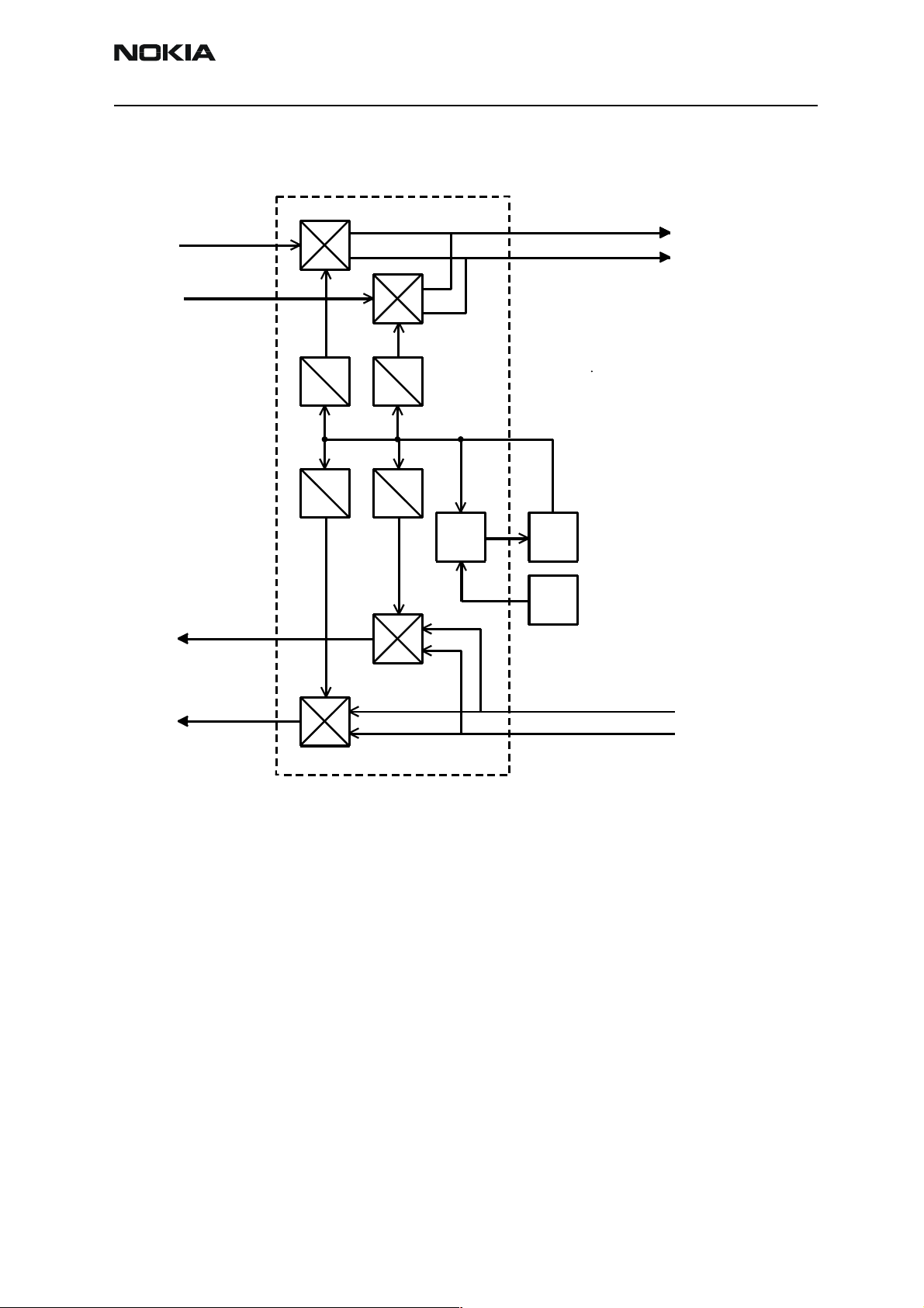
RF Block Diagram
The block diagram of the RF module can be seen in Chapter on “RF Block Diagram”. The
detailed functional description is given in the following sections
Issue 2 06/03 Nokia Corporation. Page 43
Page 44

NPM-6/6X
System Module and User Interface CCS Technical Documentation
RF Block Diagram NPM-6/6X
Figure 17: RF Block Diagram
Page 44 Nokia Corporation. Issue 2 06/03
Page 45

NPM-6/6X
CCS Technical Documentation System Module and User Interface
Frequency synthesizers
The VCO frequency is locked by a phase locked loop (PLL) and VCTCXO which is running
at 26 MHz.
The frequency of the VCTCXO is in turn locked into the frequency of the base station with
the help of an AFC voltage which is generated in UEM by an 11 bit D/A (digital-to-analog) converter.
The PLL is located in the Helga and is controlled through the RFBus.
Loop filter filters out the comparison pulses of the phase detector and generates a DC
control voltage to the VCO.
The dividers are controlled via the RFBus. RFBusData is for the data, RFBusClk is a serial
clock for the bus and RFBusEna1X is a latch enable, which stores the new data into the
dividers.
Receiver
Each receiver path is a direct conversion linear receiver.
From the antenna the received RF-signal is fed to the front end module where a diplexer
first divides the signal to two separate paths according to the band of operation: either
lower, EGSM900 or upper, GSM1800/GSM1900 path.
At each of the paths a pin-diode switch is used to select either receive or transmit mode.
At the upper band in receive mode either GSM1800 or GSM1900 path is further selected
by another pin-diode switch.
The selections are controlled by the Helga which obtains the mode/band and timing
information through the RFBus. After the switches there is a bandpass filter at each of
the receiver paths. These filters are included in the front end module, except for
GSM1900 where it is external.
Then the signal is fed to the LNAs which are integrated in the Helga in EGSM900 and
GSM1800 while in GSM1900 the LNA is external.
In GSM1900 the amplified signal is fed to a balun and thereafter to a pregain stage of
the mixer while in EGSM900 and GSM1800 the LNA’s are directly connected to the pregain stages without having SAW filters in between. The pregain stages as well as all the
following receiver blocks are integrated in the Helga. The LNAs have three gain levels.
The first one is the maximum gain, the second one is about 30 dB below the maximum,
and the last one is the off state.
After the pregain stages there are demodulator mixers at each signal path to convert the
RF signal directly down to baseband I and Q signals. Local oscillator signals for the mixers are generated by an external VCO the frequency of which is divided by two in
GSM1800 and GSM1900 and by four in EGSM900. Those frequency dividers are integrated in the Helga and in addition to the division they also provide accurate phase
Issue 2 06/03 Nokia Corporation. Page 45
Page 46

NPM-6/6X
System Module and User Interface CCS Technical Documentation
shifting by 90 degrees which is needed for the demodulator mixers.
The demodulator output signals are all differential. After the demodulators the amplifiers
convert the differential signals to single ended. Before that, they combine the signals
from the three demodulators to a single path which means that from the output of the
demodulators to the baseband interface there are just two signal paths (I and Q) which
are common to all the frequency bands of operation.
In addition, the amplifiers perform the first part of the channel filtering and AGC: they
have two gain stages, the first one with a constant gain of 12 dB and 85 kHz -3 dB
bandwidth and the second one with a switchable gain of 6 dB and -4 dB. The filters in
the amplifier blocks are active RC filters. The rest of the analog channel filtering is provided by blocks called BIQUAD.
After the amplifier and BIQUAD blocks there is another AGC-amplifier which provides a
gain control range of 42 dB in 6 dB steps.
In addition to the AGC steps, the last AGC stage also performs the real time DC offset
compensation which is needed in a direct conversion receiver.
DC offset compensation is performed during the operations called DCN1 and DCN2.
DCN1 is carried out by charging off-chip capacitors in the last AGC stages to a voltage
which causes a zero DC offset. DCN2 is used to set the signal offset to a constant value,
VrefRF_02 which is 1.35 V. That voltage level is then used as a zero level for RX ADCs
which are located in UEM.
After the last AGC and DC offset compensation stages the single ended and filtered Iand Q-signals are finally fed to the RX ADCs. The maximum peak-to-peak voltage swing
for the ADCs is 1.45 V.
In the Helga there is a port called RF-temp which can be used for compensation of RX
SAW filters thermal behavior. The temperature information to the Helga comes from a
voltage over two diodes when the diodes are fed with temperature independent, constant current.
Transmitter
The transmitter consists of two final frequency IQ-modulators and power amplifiers, for
the lower and upper bands separately, and a power control loop. The IQ-modulators are
integrated in the Helga, as well as the operational amplifiers of the power control loop.
The two power amplifiers are located in a single module which also includes the power
detector and the directional coupler. Loop filter parts of the power control loop are
implemented as discrete components on the PWB. In the GMSK mode the power is controlled by adjusting the DC bias levels of the power amplifiers.
The modulated waveforms, i.e. the I- and Q-signals, are generated by the baseband part
of the engine module. After post filtering, implemented as RC-networks, they go into the
IQ-modulator. Local oscillator signals for the modulator mixers are generated by an
external VCO the frequency of which is divided by two in GSM1800 and in GSM1900 and
Page 46 Nokia Corporation. Issue 2 06/03
Page 47

NPM-6/6X
CCS Technical Documentation System Module and User Interface
by four in EGSM900. Those frequency dividers are integrated in the Helga and in addition
to the division they also provide accurate phase shifting by 90 degrees which is needed
for the modulator mixers.
At the upper band there is a dual mode buffer amplifier at the output of the IQ-modulator. The final amplification is realized by a three stage power amplifier.
There are two different amplifier chains in a single amplifier module, one for EGSM900
and one for GSM1800/GSM1900. The lower band power amplifier is able to deliver over
2 W of RF power, while the capability of the upper band amplifier is over 1 W.
In the GMSK mode the gain control is implemented by adjusting the bias voltages of the
first two transistor stages thereby reaching the dynamic range of over 70 dB.
After the power amplifier the signal goes through a low pass filter and a pin-diode
switch which is used to select between the reception and transmission. Finally, the two
signal paths, lower and upper band, are combined in a diplexer after which the signal is
routed through the antenna.
Power control circuitry consists of a power amplifier and an error amplifier. The power
amplifier produces a voltage level related to the value of the RF voltage. It is fed to the
negative input of the error amplifier where it is compared to the level of the reference
signal, TXC, obtained from UEM. Depending on the difference between the two signals
the biases of the power amplifier stages are either increased or decreased to get the correct power level out of the power amplifier.
Front End
The front end module includes:
- Antenna 50 ohm input
- RX GSM1900 single output, RX EGSM900 and GSM1800 balanced output
- TXs EGSM900 and GSM1800/GSM1900 single 50 ohm input
-3 control lines from the Helga
Issue 2 06/03 Nokia Corporation. Page 47
Page 48

NPM-6/6X
System Module and User Interface CCS Technical Documentation
Figure 18: Front End
Ant
TX
EGSM
TX
900
DCS/PCS
GSM1800/1900
RX
RX
GSM1900
PCS
RX
RX
GSM1800
DCS
RX
EGSM
900
Power Amplifier
The power amplifier features include:
- 50 ohm input and output, EGSM900 and GSM1800/GSM1900
- internal power detector
- low and high power mode (EGSM900)
Page 48 Nokia Corporation. Issue 2 06/03
Page 49

NPM-6/6X
CCS Technical Documentation System Module and User Interface
Figure 19: Power amplifier
EGSM
out
DCS/
GSM1800/1900 GSM1800/1900
PCS
out
EGSM900 GSM1800/1900
EGSM
Power
control
DCS/PCS
Power
control
EGSM
in
DCS/
PCS
in
Power
detector
Mode
900900
RF ASIC Helga
The RF ASIC module includes:
- Package uBGA108
- Balanced I/Q demodulator and balanced I/Q modulator
- Power control operational amplifier, acts as an error amplifier
- The signal from VCO is balanced, frequencies 3420 to 3980 MHz
- EGSM900 and GSM1800 low noise amplifier (LNA) are integrated.
The Helga can be tested by test points only.
AFC function
AFC is used to lock the transceiver’s clock to the frequency of the base station.
Antenna
The NPM-6/6X EGSM900/GSM1800/GSM1900 transceiver features an internal antenna.
Issue 2 06/03 Nokia Corporation. Page 49
Page 50

NPM-6/6X
System Module and User Interface CCS Technical Documentation
This page was intentionally left blank.
Page 50 Nokia Corporation. Issue 2 06/03
 Loading...