

Page 1

Nokia Customer Care
Service Manual
RM-362; RM-363 (Nokia 5000)
Mobile Terminal
Part No: 9205778 (Issue 1)
COMPANY CONFIDENTIAL
Copyright © 2008 Nokia. All rights reserved.
Page 2

Amendment Record Sheet
Amendment Record Sheet
Amendment No Date Inserted By Comments
Issue 1 04/2008 Y Liu
RM-362; RM-363
Page ii COMPANY CONFIDENTIAL Issue 1
Copyright © 2008 Nokia. All rights reserved.
Page 3

RM-362; RM-363
Copyright
Copyright
Copyright © 2008 Nokia. All rights reserved.
Reproduction, transfer, distribution or storage of part or all of the contents in this document in any form
without the prior written permission of Nokia is prohibited.
Nokia, Nokia Connecting People, and Nokia X and Y are trademarks or registered trademarks of Nokia
Corporation. Other product and company names mentioned herein may be trademarks or tradenames of
their respective owners.
Nokia operates a policy of continuous development. Nokia reserves the right to make changes and
improvements to any of the products described in this document without prior notice.
Under no circumstances shall Nokia be responsible for any loss of data or income or any special, incidental,
consequential or indirect damages howsoever caused.
The contents of this document are provided "as is". Except as required by applicable law, no warranties of
any kind, either express or implied, including, but not limited to, the implied warranties of merchantability
and fitness for a particular purpose, are made in relation to the accuracy, reliability or contents of this
document. Nokia reserves the right to revise this document or withdraw it at any time without prior notice.
The availability of particular products may vary by region.
IMPORTANT
This document is intended for use by qualified service personnel only.
Issue 1 COMPANY CONFIDENTIAL Page iii
Copyright © 2008 Nokia. All rights reserved.
Page 4

RM-362; RM-363
Warnings and cautions
Warnings and cautions
Warnings
• IF THE DEVICE CAN BE INSTALLED IN A VEHICLE, CARE MUST BE TAKEN ON INSTALLATION IN VEHICLES FITTED
WITH ELECTRONIC ENGINE MANAGEMENT SYSTEMS AND ANTI-SKID BRAKING SYSTEMS. UNDER CERTAIN FAULT
CONDITIONS, EMITTED RF ENERGY CAN AFFECT THEIR OPERATION. IF NECESSARY, CONSULT THE VEHICLE DEALER/
MANUFACTURER TO DETERMINE THE IMMUNITY OF VEHICLE ELECTRONIC SYSTEMS TO RF ENERGY.
• THE PRODUCT MUST NOT BE OPERATED IN AREAS LIKELY TO CONTAIN POTENTIALLY EXPLOSIVE ATMOSPHERES,
FOR EXAMPLE, PETROL STATIONS (SERVICE STATIONS), BLASTING AREAS ETC.
• OPERATION OF ANY RADIO TRANSMITTING EQUIPMENT, INCLUDING CELLULAR TELEPHONES, MAY INTERFERE
WITH THE FUNCTIONALITY OF INADEQUATELY PROTECTED MEDICAL DEVICES. CONSULT A PHYSICIAN OR THE
MANUFACTURER OF THE MEDICAL DEVICE IF YOU HAVE ANY QUESTIONS. OTHER ELECTRONIC EQUIPMENT MAY
ALSO BE SUBJECT TO INTERFERENCE.
• BEFORE MAKING ANY TEST CONNECTIONS, MAKE SURE YOU HAVE SWITCHED OFF ALL EQUIPMENT.
Cautions
• Servicing and alignment must be undertaken by qualified personnel only.
• Ensure all work is carried out at an anti-static workstation and that an anti-static wrist strap is worn.
• Ensure solder, wire, or foreign matter does not enter the telephone as damage may result.
• Use only approved components as specified in the parts list.
• Ensure all components, modules, screws and insulators are correctly re-fitted after servicing and
alignment.
• Ensure all cables and wires are repositioned correctly.
• Never test a mobile phone WCDMA transmitter with full Tx power, if there is no possibility to perform the
measurements in a good performance RF-shielded room. Even low power WCDMA transmitters may disturb
nearby WCDMA networks and cause problems to 3G cellular phone communication in a wide area.
• During testing never activate the GSM or WCDMA transmitter without a proper antenna load, otherwise
GSM or WCDMA PA may be damaged.
Page iv COMPANY CONFIDENTIAL Issue 1
Copyright © 2008 Nokia. All rights reserved.
Page 5

RM-362; RM-363
For your safety
For your safety
QUALIFIED SERVICE
Only qualified personnel may install or repair phone equipment.
ACCESSORIES AND BATTERIES
Use only approved accessories and batteries. Do not connect incompatible products.
CONNECTING TO OTHER DEVICES
When connecting to any other device, read its user’s guide for detailed safety instructions. Do not connect
incompatible products.
Issue 1 COMPANY CONFIDENTIAL Page v
Copyright © 2008 Nokia. All rights reserved.
Page 6

RM-362; RM-363
Care and maintenance
Care and maintenance
This product is of superior design and craftsmanship and should be treated with care. The suggestions below
will help you to fulfil any warranty obligations and to enjoy this product for many years.
• Keep the phone and all its parts and accessories out of the reach of small children.
• Keep the phone dry. Precipitation, humidity and all types of liquids or moisture can contain minerals that
will corrode electronic circuits.
• Do not use or store the phone in dusty, dirty areas. Its moving parts can be damaged.
• Do not store the phone in hot areas. High temperatures can shorten the life of electronic devices, damage
batteries, and warp or melt certain plastics.
• Do not store the phone in cold areas. When it warms up (to its normal temperature), moisture can form
inside, which may damage electronic circuit boards.
• Do not drop, knock or shake the phone. Rough handling can break internal circuit boards.
• Do not use harsh chemicals, cleaning solvents, or strong detergents to clean the phone.
• Do not paint the phone. Paint can clog the moving parts and prevent proper operation.
• Use only the supplied or an approved replacement antenna. Unauthorised antennas, modifications or
attachments could damage the phone and may violate regulations governing radio devices.
All of the above suggestions apply equally to the product, battery, charger or any accessory.
Page vi COMPANY CONFIDENTIAL Issue 1
Copyright © 2008 Nokia. All rights reserved.
Page 7

RM-362; RM-363
ESD protection
ESD protection
Nokia requires that service points have sufficient ESD protection (against static electricity) when servicing
the phone.
Any product of which the covers are removed must be handled with ESD protection. The SIM card can be
replaced without ESD protection if the product is otherwise ready for use.
To replace the covers ESD protection must be applied.
All electronic parts of the product are susceptible to ESD. Resistors, too, can be damaged by static electricity
discharge.
All ESD sensitive parts must be packed in metallized protective bags during shipping and handling outside
any ESD Protected Area (EPA).
Every repair action involving opening the product or handling the product components must be done under
ESD protection.
ESD protected spare part packages MUST NOT be opened/closed out of an ESD Protected Area.
For more information and local requirements about ESD protection and ESD Protected Area, contact your local
Nokia After Market Services representative.
Issue 1 COMPANY CONFIDENTIAL Page vii
Copyright © 2008 Nokia. All rights reserved.
Page 8

RM-362; RM-363
Battery information
Battery information
Note: A new battery's full performance is achieved only after two or three complete charge and
discharge cycles!
The battery can be charged and discharged hundreds of times but it will eventually wear out. When the
operating time (talk-time and standby time) is noticeably shorter than normal, it is time to buy a new battery.
Use only batteries approved by the phone manufacturer and recharge the battery only with the chargers
approved by the manufacturer. Unplug the charger when not in use. Do not leave the battery connected to
a charger for longer than a week, since overcharging may shorten its lifetime. If left unused a fully charged
battery will discharge itself over time.
Temperature extremes can affect the ability of your battery to charge.
For good operation times with Ni-Cd/NiMh batteries, discharge the battery from time to time by leaving the
product switched on until it turns itself off (or by using the battery discharge facility of any approved accessory
available for the product). Do not attempt to discharge the battery by any other means.
Use the battery only for its intended purpose.
Never use any charger or battery which is damaged.
Do not short-circuit the battery. Accidental short-circuiting can occur when a metallic object (coin, clip or
pen) causes direct connection of the + and - terminals of the battery (metal strips on the battery) for example
when you carry a spare battery in your pocket or purse. Short-circuiting the terminals may damage the battery
or the connecting object.
Leaving the battery in hot or cold places, such as in a closed car in summer or winter conditions, will reduce
the capacity and lifetime of the battery. Always try to keep the battery between 15°C and 25°C (59°F and 77°
F). A phone with a hot or cold battery may temporarily not work, even when the battery is fully charged.
Batteries' performance is particularly limited in temperatures well below freezing.
Do not dispose of batteries in a fire!
Dispose of batteries according to local regulations (e.g. recycling). Do not dispose as household waste.
Page viii COMPANY CONFIDENTIAL Issue 1
Copyright © 2008 Nokia. All rights reserved.
Page 9

RM-362; RM-363
Company Policy
Company Policy
Our policy is of continuous development; details of all technical modifications will be included with service
bulletins.
While every endeavour has been made to ensure the accuracy of this document, some errors may exist. If
any errors are found by the reader, NOKIA MOBILE PHONES Business Group should be notified in writing/email.
Please state:
• Title of the Document + Issue Number/Date of publication
• Latest Amendment Number (if applicable)
• Page(s) and/or Figure(s) in error
Please send to:
NOKIA CORPORATION
Nokia Mobile Phones Business Group
Nokia Customer Care
PO Box 86
FIN-24101 SALO
Finland
E-mail: Service.Manuals@nokia.com
Issue 1 COMPANY CONFIDENTIAL Page ix
Copyright © 2008 Nokia. All rights reserved.
Page 10

RM-362; RM-363
Company Policy
(This page left intentionally blank.)
Page x COMPANY CONFIDENTIAL Issue 1
Copyright © 2008 Nokia. All rights reserved.
Page 11

RM-362; RM-363
Nokia 5000 Service Manual Structure
Nokia 5000 Service Manual Structure
1 General Information
2 Service Devices and Service Concepts
3 Baseband Troubleshooting Instructions
4 RF Troubleshooting Instructions
5 Camera Module Troubleshooting
6 System Module
Glossary
Issue 1 COMPANY CONFIDENTIAL Page xi
Copyright © 2008 Nokia. All rights reserved.
Page 12

RM-362; RM-363
Nokia 5000 Service Manual Structure
(This page left intentionally blank.)
Page xii COMPANY CONFIDENTIAL Issue 1
Copyright © 2008 Nokia. All rights reserved.
Page 13

Nokia Customer Care
1 — General Information
Issue 1 COMPANY CONFIDENTIAL Page 1 –1
Copyright © 2008 Nokia. All rights reserved.
Page 14

RM-362; RM-363
General Information
(This page left intentionally blank.)
Page 1 –2 COMPANY CONFIDENTIAL Issue 1
Copyright © 2008 Nokia. All rights reserved.
Page 15

RM-362; RM-363
General Information
Table of Contents
RM-362/RM-363 product selection .......................................................................................................................1–5
Features...................................................................................................................................................................1–5
Hardware features ............................................................................................................................................1–5
Software features..............................................................................................................................................1–6
UI features..........................................................................................................................................................1–6
Mobile enhancements.......................................................................................................................................1–6
List of Tables
Table 1 Power.........................................................................................................................................................1–6
Table 2 Car...............................................................................................................................................................1–6
Table 3 Audio..........................................................................................................................................................1–7
List of Figures
Figure 1 RM-362/363 product picture ..................................................................................................................1–5
Issue 1 COMPANY CONFIDENTIAL Page 1 –3
Copyright © 2008 Nokia. All rights reserved.
Page 16

RM-362; RM-363
General Information
(This page left intentionally blank.)
Page 1 –4 COMPANY CONFIDENTIAL Issue 1
Copyright © 2008 Nokia. All rights reserved.
Page 17
RM-362; RM-363
General Information
RM-362/RM-363 product selection
The RM-362 is the EU version of the telephone with a dual band transceiver unit designed for the GSM900
and GSM1800 networks.
The RM-363 is the US version of the telephone with a dual band transceiver unit designed for the GSM850
and GSM1900 networks.
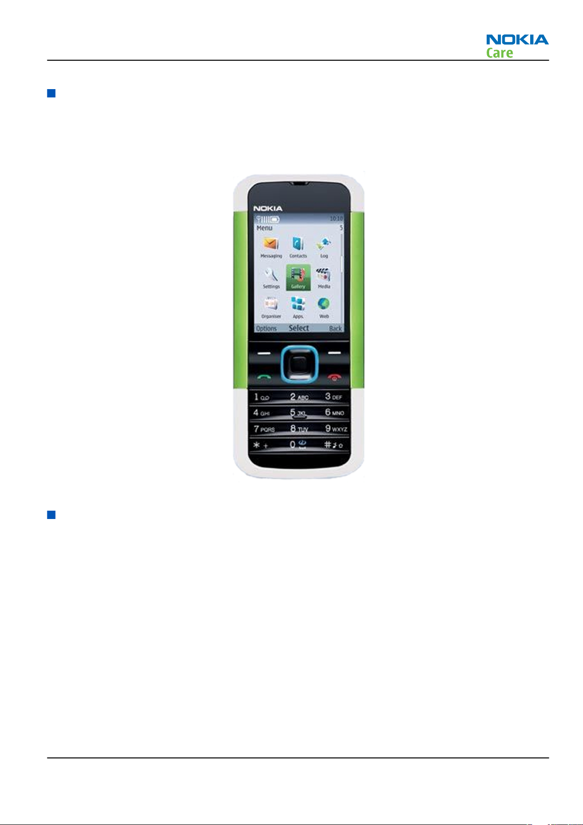
Figure 1 RM-362/363 product picture
Features
Hardware features
• EGSM dualband 900/1800 for EMEA, APAC, China, LTA·
• GSM dualband 850/1900 for LTA
• Display: 320x240 TFT color display
• Codecs: HR, FR, EFR and AMR
• IHF Slim Malt 16mm Speaker
• Internal antenna
• Easy flash II system connector
• BT combined with FM radio
• 1.3 MPix camera
• Built-in Vibra
• GPRS: Class 6
Issue 1 COMPANY CONFIDENTIAL Page 1 –5
Copyright © 2008 Nokia. All rights reserved.
Page 18
Software features
• OS: ISA
• UI Style: S40
• MIDP 2.0 Java, with latest APIs
• Browser: XHTML over TCP/IP (WAP 2.0 compliant)
• Video capture and playback (7.5fps, H.263; MPEG4)
• MMS 1.2
• English-Chinese dictionary for China/APAC
• E-mail Client 4
• Nokia Xpress audio messaging
UI features
• Douglas 8 UI style with 3 soft keysl
• Nokia Series 40 user interface
• MP3&AAC ringing tones & 24 polyphonic ringing tones
• Themes, colour games and wall papers
• Java games (downloadable)
• To-do list and Notes
• Countdown timer
• Phonebook image
• Menu with animated icons
• 2 font sizes are supported in the editor
• Calendar in day/week/month view
• Chinese lunar Calendar II (not for all regions)
• “Pulsating light” indicating missed call, unread messages, etc.
RM-362; RM-363
General Information
Mobile enhancements
Table 1 Power
Type Name
BL-4B Battery 700 mAh Li-Ion
AC-3 Compact charger
AC-4 Travel charger
AC-5 Compact travel charger
CA-44 Charger adapter
DC-4 Mobile charger
Table 2 Car
Type Name
CK-15W Display car kit
Page 1 –6 COMPANY CONFIDENTIAL Issue 1
Copyright © 2008 Nokia. All rights reserved.
Page 19
RM-362; RM-363
General Information
Type Name
CK-20W Multimedia car kit
CK-25W Multimedia car kit
Table 3 Audio
Type Name
HS-38W Nokia bluetooth headset BH-202
HS-40 Headset
HS-47 Stereo headset
HS-50W Nokia bluetooth headset BH-300
HS-51W Nokia bluetooth headset BH-301
HS-52W Nokia bluetooth headset BH-201
HS-58W Nokia bluetooth headset BH-200
HS-68W Nokia bluetooth headset BH-203
HS-73W Nokia bluetooth headset BH-302
HS-78W Nokia bluetooth headset BH-100
HS-79W Nokia bluetooth headset BH-303
HS-80W Nokia bluetooth headset BH-208
HS-84W/88W Nokia bluetooth headset BH-204
HS-85W Nokia bluetooth headset BH-206
HS-86W Nokia bluetooth headset BH-207
MD-4 Mini speakers
Issue 1 COMPANY CONFIDENTIAL Page 1 –7
Copyright © 2008 Nokia. All rights reserved.
Page 20

RM-362; RM-363
General Information
(This page left intentionally blank.)
Page 1 –8 COMPANY CONFIDENTIAL Issue 1
Copyright © 2008 Nokia. All rights reserved.
Page 21

Nokia Customer Care
2 — Service Devices and
Service Concepts
Issue 1 COMPANY CONFIDENTIAL Page 2 –1
Copyright © 2008 Nokia. All rights reserved.
Page 22

RM-362; RM-363
Service Devices and Service Concepts
(This page left intentionally blank.)
Page 2 –2 COMPANY CONFIDENTIAL Issue 1
Copyright © 2008 Nokia. All rights reserved.
Page 23

RM-362; RM-363
Service Devices and Service Concepts
Table of Contents
Service devices........................................................................................................................................................2–5
CA-106DS ............................................................................................................................................................2–5
CA-111DS ............................................................................................................................................................2–5
CA-112DS ............................................................................................................................................................2–5
CA-41PS...............................................................................................................................................................2–6
CA-52PS...............................................................................................................................................................2–6
CA-58RS...............................................................................................................................................................2–6
DA-69 ..................................................................................................................................................................2–6
DAU-9S................................................................................................................................................................2–7
FLS-4S..................................................................................................................................................................2–7
FLS-5 ...................................................................................................................................................................2–7
FPS-10.................................................................................................................................................................2–8
JBV-1 ...................................................................................................................................................................2–8
MJ-168.................................................................................................................................................................2–9
PCS-1...................................................................................................................................................................2–9
PK-1.................................................................................................................................................................. 2–10
PKD-1 ............................................................................................................................................................... 2–10
RJ-230 .............................................................................................................................................................. 2–10
RJ-51 ................................................................................................................................................................ 2–10
RJ-72 ................................................................................................................................................................ 2–10
SA-93................................................................................................................................................................ 2–11
SRT-6................................................................................................................................................................ 2–11
SS-88................................................................................................................................................................ 2–11
SS-93................................................................................................................................................................ 2–11
ST-30................................................................................................................................................................ 2–12
ST-32................................................................................................................................................................ 2–12
SX-4.................................................................................................................................................................. 2–12
XCS-4 ................................................................................................................................................................ 2–12
XRS-6................................................................................................................................................................ 2–12
Service concepts .................................................................................................................................................. 2–13
POS flash concept with FLS-4S....................................................................................................................... 2–13
POS flash concept with FLS-5 ........................................................................................................................ 2–14
Flash concept with FPS-10............................................................................................................................. 2–15
RF-test/BB-tune concept with JBV-1............................................................................................................. 2–16
EM calibration concept with JBV-1................................................................................................................ 2–17
RF-test/BB-tune & flash concept with JBV-1, FPS-10................................................................................... 2–18
RF/BB tune& flash concept with MJ-137, FPS-10......................................................................................... 2–19
List of Figures
Figure 2 POS flash concept with FLS-4S............................................................................................................. 2–13
Figure 3 POS flash concept with FLS-5............................................................................................................... 2–14
Figure 4 Flash concept with FPS-10................................................................................................................... 2–15
Figure 5 RF-test/BB-tune concept with JBV-1................................................................................................... 2–16
Figure 6 EM calibration concept with JBV-1...................................................................................................... 2–17
Figure 7 RF-test/BB-tune & flash concept with JBV-1, FPS-10......................................................................... 2–18
Figure 8 RF/BB tune& flash concept with MJ-137, FPS-10 ............................................................................... 2–19
Issue 1 COMPANY CONFIDENTIAL Page 2 –3
Copyright © 2008 Nokia. All rights reserved.
Page 24

RM-362; RM-363
Service Devices and Service Concepts
(This page left intentionally blank.)
Page 2 –4 COMPANY CONFIDENTIAL Issue 1
Copyright © 2008 Nokia. All rights reserved.
Page 25
RM-362; RM-363
Service Devices and Service Concepts
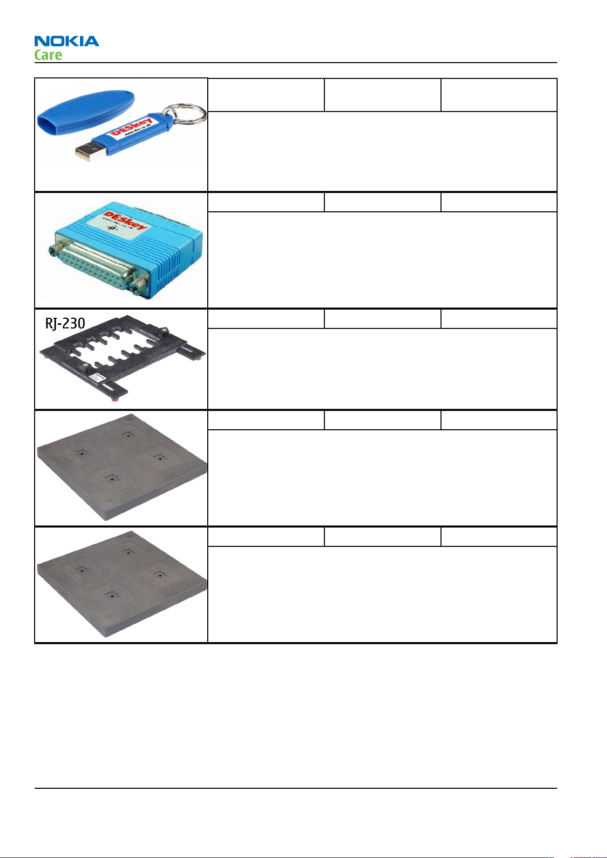
Service devices
The table below gives a short overview of service devices that can be used for testing, error analysis, and
repair of product RM-362; RM-363. For the correct use of the service devices, and the best effort of workbench
setup, please refer to various concepts.
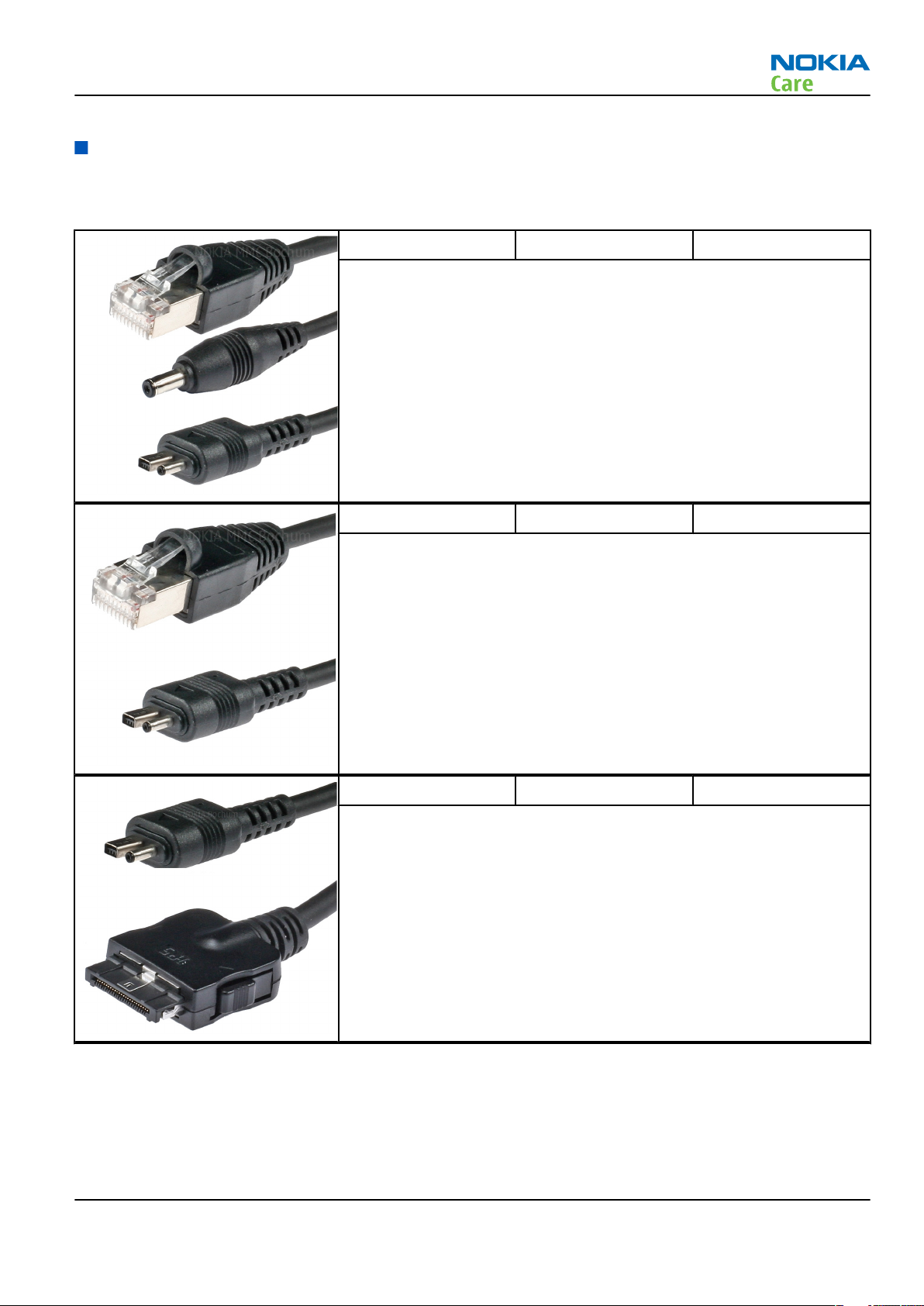
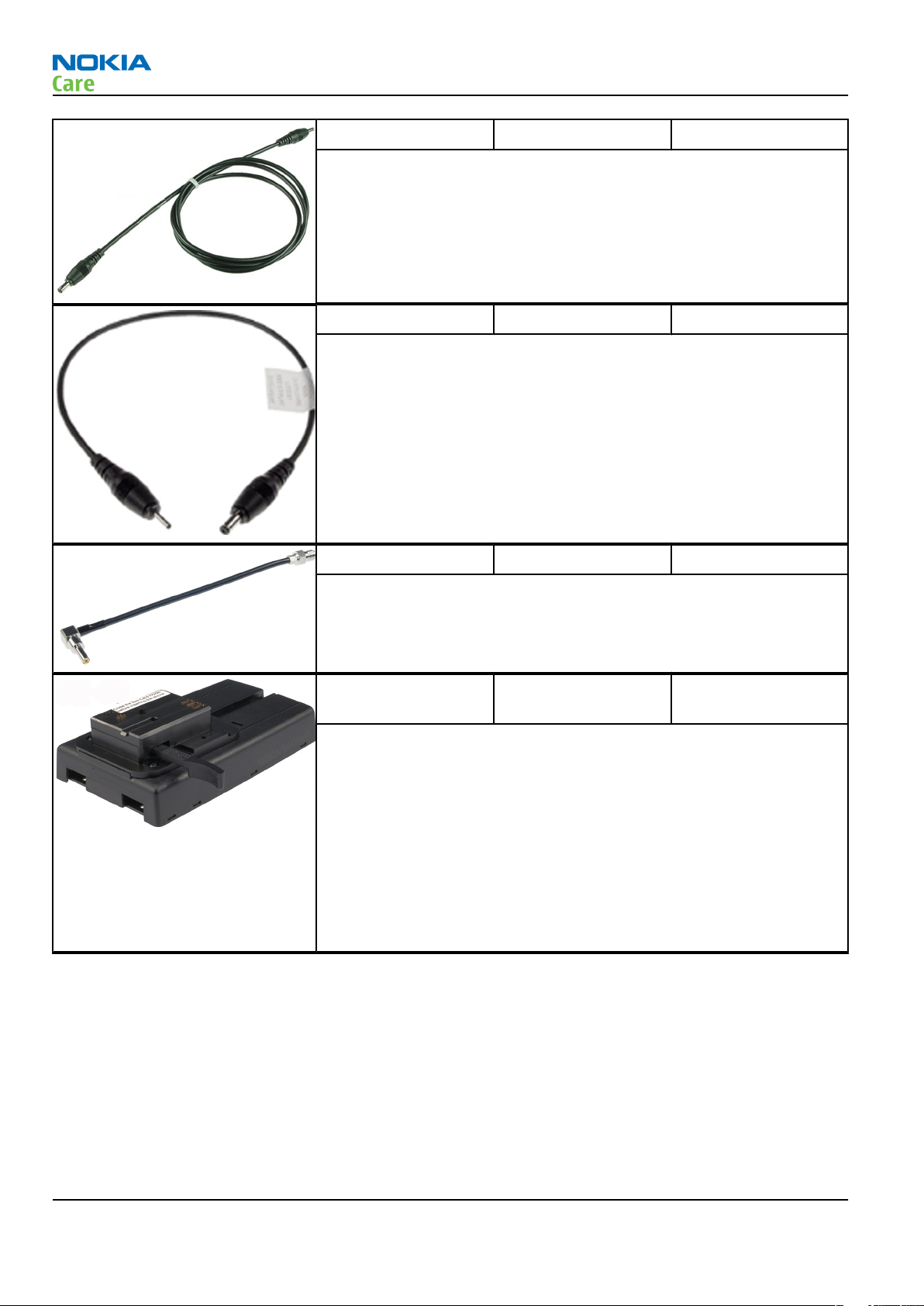
CA-106DS Easy flash II cable The cable is used for connecting phone DC port to the flash prommer
FPS-10.
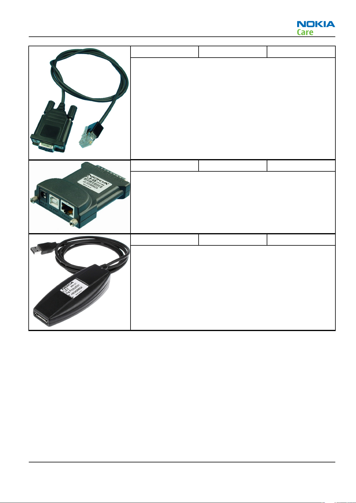
CA-111DS Easy flash II cable The cable is used for connecting phone DC port to either POS flashing
device FLS-4S or to the PROMMER box FPS-11.
CA-112DS Easy flash II cable The CA-112DS easy flash II cable is used for connecting phone DC port
to the PROMMER facilities (FLS-5, FPS-20).
Issue 1 COMPANY CONFIDENTIAL Page 2 –5
Copyright © 2008 Nokia. All rights reserved.
Page 26
RM-362; RM-363
Service Devices and Service Concepts
CA-41PS Power cable Power cable for connection of e.g. the JBV-1 docking station to the
FPS-10 prommer box.
CA-52PS DC Cable The cable is used to connect JBV-1 docking station to the phone
charger jack for ADC/VCHAR/ICHAR calibration.
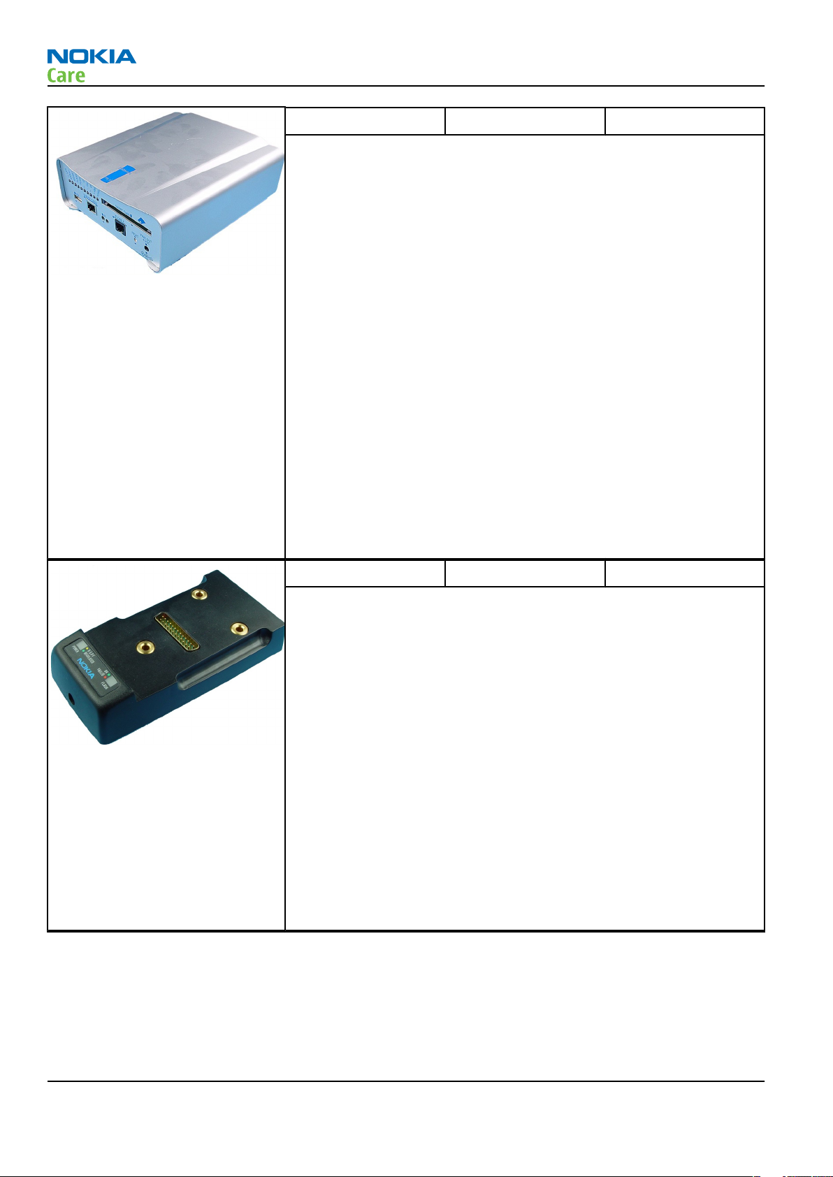
CA-58RS RF Cable This RF cable is used together with MJ-138 to connect to RF
measurement equipment.
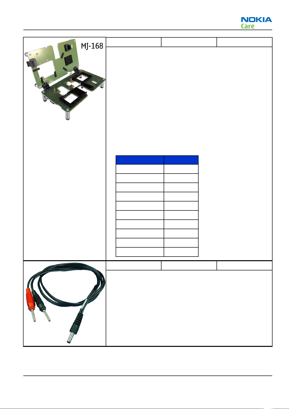
DA-69 Docking station
adapter
The docking station adapter is used for this phone in combination with
JBV-1. The adapter supports flashing and energy management
calibration,
Features include:
• compatible with JBV-1
• easy phone attachment and detachment
• reliable phone locking
• switch for detecting phone
• replaceable SIM interface
Page 2 –6 COMPANY CONFIDENTIAL Issue 1
Copyright © 2008 Nokia. All rights reserved.
Page 27
RM-362; RM-363
Service Devices and Service Concepts
DAU-9S MBUS cable The MBUS cable DAU-9S has a modular connector and is used, for
example, between the PC's serial port and module jigs, flash adapters
or docking station adapters.
Note: Docking station adapters valid for DCT4 products.
FLS-4S Flash device FLS-4S is a dongle and flash device incorporated into one package,
developed specifically for POS use.
FLS-5 Flash device FLS-5 is a dongle and flash device incorporated into one package,
developed specifically for POS use.
Note: FLS-5 can be used as an alternative to PKD-1.
Issue 1 COMPANY CONFIDENTIAL Page 2 –7
Copyright © 2008 Nokia. All rights reserved.
Page 28
Service Devices and Service Concepts
FPS-10 Flash prommer FPS-10 interfaces with:
• PC
• Control unit
• Flash adapter
• Smart card
FPS-10 flash prommer features:
• Flash functionality for BB5 and DCT-4 terminals
• Smart Card reader for SX-2 or SX-4
• USB traffic forwarding
• USB to FBUS/Flashbus conversion
• LAN to FBUS/Flashbus and USB conversion
• Vusb output switchable by PC command
FPS-10 sales package includes:
• FPS-10 prommer
• Power Supply with 5 country specific cords
• USB cable
Note: FPS-21 is substitute FPS-10 if FPS-10 has not been set
up.
RM-362; RM-363
JBV-1 Docking station The JBV-1 docking station is a general tool that has been designed for
calibration and software update use. The JBV-1 is used together with
a docking station adapter as one unit
In calibration mode the JBV-1 is powered by an external power supply:
11-16V DC. When flashing the power for the phone must be taken from
the flash prommer.
Note: JBV-1 main electrical functions are:
• adjustable VBATT calibration voltage, current
measurement limit voltage: VCHAR, current measurement:
ICHAR
• adjustable ADC calibration voltage via BTEM and the BSI
signal
• BTEMP and BSI calibration resistor
• signal from FBUS to the phone via the parallel jig
• control via FBUS or USB
• Flash OK/FAIL indication
Page 2 –8 COMPANY CONFIDENTIAL Issue 1
Copyright © 2008 Nokia. All rights reserved.
Page 29
RM-362; RM-363
Service Devices and Service Concepts
MJ-168 Module jig MJ-168 is meant for component level troubleshooting.
The jig includes an RF interface for GSM and Bluetooth. in addition, it
has the following features:
• Provides mechanical interface with the engine and UI module
• Provides galvanic connection to all needed test pads in module
• Duplicated SIM connector
• Audio components: IHF, MIC
• Connector for control unit
Note: CA-58RS(RF cable) is used together with MJ-168.
CA-58RS is not a part of the MJ-168 sales package and has to
be ordered separately.
Note: Please remove the shield frame before audio testing
by Easy Flash II connector.
The following table shows the attenuation values for MJ-168:
•
Frequency (Hz) Loss (dB)
836600000 0.24
881600000 0.24
897400000 0.25
942400000 0.25
1747800000 0.35
1842800000 0.37
1880000000 0.38
1950000000 0.40
1960000000 0.40
2140000000 0.40
PCS-1 Power cable The PCS-1 power cable (DC) is used with a docking station, a module
jig or a control unit to supply a controlled voltage.
Issue 1 COMPANY CONFIDENTIAL Page 2 –9
Copyright © 2008 Nokia. All rights reserved.
Page 30
RM-362; RM-363
Service Devices and Service Concepts
PK-1 Software protection
key
PK-1 is a hardware protection key with a USB interface. It has the same
functionality as the PKD-1 series dongle.
PK-1 is meant for use with a PC that does not have a series interface.
To use this USB dongle for security service functions please register
the dongle in the same way as the PKD-1 series dongle.
PKD-1 SW security device
SW security device is a piece of hardware enabling the use of the
service software when connected to the parallel (LPT) port of the PC.
Without the device, it is not possible to use the service software.
Printer or any such device can be connected to the PC through the
device if needed.
RJ-230 Soldering jig RJ-230 is a soldering jig used for soldering and as a rework jig for the
engine module.
RJ-51 Rework jig To be used with ST-30!
RJ-72 Rework jig To be used with rework stencil ST-32.
Page 2 –10 COMPANY CONFIDENTIAL Issue 1
Copyright © 2008 Nokia. All rights reserved.
Page 31

RM-362; RM-363
Service Devices and Service Concepts
SA-93 RF coupler The coupler is used for Go/No-Go test after changing components in
the RF part of the phone.
It is mounted on the docking station adapter.
The following table shows attenuations from the antenna pads of the
mobile terminal to the SMA connectors of SA-93:
•
Band Tuning
channel
GSM850 128 6 6
190 7 6
251 7 6
GSM900 38 11 7
124 13 7
975 10 8
GSM1800 512 7 7
Attenuation RX
(dB)
Attenuation
TX(dB)
700 6 7
885 6 7
GSM1900 512 6 6
661 7 6
810 9 6
SRT-6 Opening tool SRT-6 is used to open phone covers and B-to-B connectors.
Caution: Handle the tool with care because the tip is only 0.7
mm in diameter.
When not in use, store in a safe location.
SS-88 Camera removal tool The camera removal tool SS-88 is used to remove/attach the front
camera module from/to the socket.
SS-93 Opening tool SS-93 is used for opening JAE connectors.
Issue 1 COMPANY CONFIDENTIAL Page 2 –11
Copyright © 2008 Nokia. All rights reserved.
Page 32

RM-362; RM-363
Service Devices and Service Concepts
ST-30 Rework stencil It is used together with RJ-51 to rework N7700.
ST-32 Rework stencil for
B2100
Rework stencil to be used together with RJ-72 for rework of N7600.
SX-4 Smart card SX-4 is a BB5 security device used to protect critical features in tuning
and testing.
SX-4 is also needed together with FPS-10 when DCT-4 phones are
flashed.
XCS-4 Modular cable XCS-4 is a shielded (one specially shielded conductor) modular cable
for flashing and service purposes.
XRS-6 RF cable The RF cable is used to connect, for example, a module repair jig to
the RF measurement equipment.
SMA to N-Connector approximately 610 mm.
Attenuation for:
• GSM850/900: 0.3+-0.1 dB
• GSM1800/1900: 0.5+-0.1 dB
• WLAN: 0.6+-0.1dB
Page 2 –12 COMPANY CONFIDENTIAL Issue 1
Copyright © 2008 Nokia. All rights reserved.
Page 33

RM-362; RM-363
Service Devices and Service Concepts
Service concepts
POS flash concept with FLS-4S
Figure 2 POS flash concept with FLS-4S
Issue 1 COMPANY CONFIDENTIAL Page 2 –13
Copyright © 2008 Nokia. All rights reserved.
Page 34

POS flash concept with FLS-5
RM-362; RM-363
Service Devices and Service Concepts
Figure 3 POS flash concept with FLS-5
Page 2 –14 COMPANY CONFIDENTIAL Issue 1
Copyright © 2008 Nokia. All rights reserved.
Page 35

RM-362; RM-363
Service Devices and Service Concepts
Flash concept with FPS-10
Figure 4 Flash concept with FPS-10
Issue 1 COMPANY CONFIDENTIAL Page 2 –15
Copyright © 2008 Nokia. All rights reserved.
Page 36

RF-test/BB-tune concept with JBV-1
RM-362; RM-363
Service Devices and Service Concepts
Figure 5 RF-test/BB-tune concept with JBV-1
Page 2 –16 COMPANY CONFIDENTIAL Issue 1
Copyright © 2008 Nokia. All rights reserved.
Page 37

RM-362; RM-363
Service Devices and Service Concepts
EM calibration concept with JBV-1
Figure 6 EM calibration concept with JBV-1
Issue 1 COMPANY CONFIDENTIAL Page 2 –17
Copyright © 2008 Nokia. All rights reserved.
Page 38

RF-test/BB-tune & flash concept with JBV-1, FPS-10
RM-362; RM-363
Service Devices and Service Concepts
Figure 7 RF-test/BB-tune & flash concept with JBV-1, FPS-10
Page 2 –18 COMPANY CONFIDENTIAL Issue 1
Copyright © 2008 Nokia. All rights reserved.
Page 39

RM-362; RM-363
Service Devices and Service Concepts
RF/BB tune& flash concept with MJ-137, FPS-10
Figure 8 RF/BB tune& flash concept with MJ-137, FPS-10
Issue 1 COMPANY CONFIDENTIAL Page 2 –19
Copyright © 2008 Nokia. All rights reserved.
Page 40

RM-362; RM-363
Service Devices and Service Concepts
(This page left intentionally blank.)
Page 2 –20 COMPANY CONFIDENTIAL Issue 1
Copyright © 2008 Nokia. All rights reserved.
Page 41

Nokia Customer Care
3 — Baseband
Troubleshooting Instructions
Issue 1 COMPANY CONFIDENTIAL Page 3 –1
Copyright © 2008 Nokia. All rights reserved.
Page 42

RM-362; RM-363
Baseband Troubleshooting Instructions
(This page left intentionally blank.)
Page 3 –2 COMPANY CONFIDENTIAL Issue 1
Copyright © 2008 Nokia. All rights reserved.
Page 43

RM-362; RM-363
Baseband Troubleshooting Instructions
Table of Contents
General baseband troubleshooting......................................................................................................................3–5
Key components................................................................................................................................................3–5
Power supply test points..................................................................................................................................3–5
Phone cannot be powered on (I).....................................................................................................................3–6
Phone cannot be powered on (II)....................................................................................................................3–8
Phone cannot be flashed..................................................................................................................................3–9
Easy flash programming does not work...................................................................................................... 3–11
Display shows "Contact Service"................................................................................................................... 3–13
The phone does not register to the networks, or the phone cannot make a call................................... 3–14
SIM related faults................................................................................................................................................. 3–16
Insert SIM card fault....................................................................................................................................... 3–16
SIM card rejected............................................................................................................................................ 3–17
User interface....................................................................................................................................................... 3–17
Blank display................................................................................................................................................... 3–17
Corrupted display ........................................................................................................................................... 3–18
Dead keys ........................................................................................................................................................ 3–18
No backlight for display or/and keys ........................................................................................................... 3–19
Audio troubleshooting........................................................................................................................................ 3–20
Audio troubleshooting using phoenix......................................................................................................... 3–20
Check microphone using "Hp microphone in Ext speaker out" loop ........................................................ 3–21
Check earpiece using "Ext microphone in Hp speaker out" loop .............................................................. 3–22
Check IHF & ringing tone function using "Buzzer"...................................................................................... 3–22
Check vibra function using "Vibra control".................................................................................................. 3–23
Earpiece fault.................................................................................................................................................. 3–24
IHF/ringing tone fault.................................................................................................................................... 3–25
Microphone fault ............................................................................................................................................ 3–26
Headset earpiece fault................................................................................................................................... 3–27
Headset microphone fault............................................................................................................................. 3–28
List of Tables
Table 4 Connector for External Audio Accessories ........................................................................................... 3–21
List of Figures
Figure 9 Troubleshooting when phone cannot be powered on .......................................................................3–7
Figure 10 Troubleshooting when phone does not stay on or phone is jammed ............................................3–8
Figure 11 Flash programming fault................................................................................................................... 3–10
Figure 12 Easy flash programming fault........................................................................................................... 3–12
Figure 13 Troubleshooting when the "Contact Service" message is seen .................................................... 3–14
Figure 14 No registering or call ......................................................................................................................... 3–15
Figure 15 Insert SIM card fault........................................................................................................................... 3–16
Figure 16 Signal diagram ................................................................................................................................... 3–17
Figure 17 Signal diagram ................................................................................................................................... 3–17
Figure 18 Phoenix audio test window.............................................................................................................. 3–20
Figure 19 4-pole jack plug for audio accessory................................................................................................ 3–21
Figure 20 Test arrangement for microphone................................................................................................... 3–22
Figure 21 Test arrangement for of earpiece..................................................................................................... 3–22
Figure 22 Checking IHF and ring tone by using "Buzzer"................................................................................ 3–23
Figure 23 Checking vibra function by using vibra control .............................................................................. 3–23
Issue 1 COMPANY CONFIDENTIAL Page 3 –3
Copyright © 2008 Nokia. All rights reserved.
Page 44

RM-362; RM-363
Baseband Troubleshooting Instructions
Figure 24 Earpiece fault flow chart ................................................................................................................... 3–24
Figure 25 IHF/ringing tone fault flow chart...................................................................................................... 3–25
Figure 26 Microphone fault flow chart.............................................................................................................. 3–26
Figure 27 Headset earpiece fault flow chart .................................................................................................... 3–27
Figure 28 Headset microphone fault flow chart .............................................................................................. 3–28
Page 3 –4 COMPANY CONFIDENTIAL Issue 1
Copyright © 2008 Nokia. All rights reserved.
Page 45

RM-362; RM-363
Baseband Troubleshooting Instructions
General baseband troubleshooting
Key components
Power supply test points
Issue 1 COMPANY CONFIDENTIAL Page 3 –5
Copyright © 2008 Nokia. All rights reserved.
Page 46

RM-362; RM-363
Baseband Troubleshooting Instructions
Phone cannot be powered on (I)
Context
This means that the phone does not use any current at all when the supply is connected and/or power key
is pressed. It is assumed that the voltage supplied is 3.6VDC. The UEMCLite will prevent any functionality at
battery/supply levels below 2.9VDC.
Page 3 –6 COMPANY CONFIDENTIAL Issue 1
Copyright © 2008 Nokia. All rights reserved.
Page 47

RM-362; RM-363
Baseband Troubleshooting Instructions
Troubleshooting flow
Figure 9 Troubleshooting when phone cannot be powered on
Issue 1 COMPANY CONFIDENTIAL Page 3 –7
Copyright © 2008 Nokia. All rights reserved.
Page 48

RM-362; RM-363
Baseband Troubleshooting Instructions
Phone cannot be powered on (II)
Context
If this kind of failure is presenting itself immediately after FLALI, it is most likely caused by ASIC's missing
contact with PWB.
If the MCU doesn’t service the watchdog register within the UEMCLite, the operations watchdog will run out
after approximately 32 seconds. Unfortunately, the service routine can not be measured.
Troubleshooting flow
Figure 10 Troubleshooting when phone does not stay on or phone is jammed
Page 3 –8 COMPANY CONFIDENTIAL Issue 1
Copyright © 2008 Nokia. All rights reserved.
Page 49

RM-362; RM-363
Baseband Troubleshooting Instructions
Phone cannot be flashed
Context
The flash programming can be done via the pads on the PWB (J2060). If failed, then follow up the trouble
shooting flow chart.
In case of flash failure in the FLALI station, swap the phone and send it back to the care program for further
analysis. Possible failures could be short-circuit of balls under µBGAs (UEMCLite, UPP4M, FLASH), or missing
or misaligned components.
In flash programming error cases, the flash prommer can give some information about a fault. The fault
information messages could be:
Phone doesn't set FBUS_TX line low
Because of the use of uBGA components, it is not possible to verify if there is a short circuit in the control and
address lines of MCU (UPP8M) and the memory (flash).
Issue 1 COMPANY CONFIDENTIAL Page 3 –9
Copyright © 2008 Nokia. All rights reserved.
Page 50

Troubleshooting flow
RM-362; RM-363
Baseband Troubleshooting Instructions
Figure 11 Flash programming fault
Page 3 –10 COMPANY CONFIDENTIAL Issue 1
Copyright © 2008 Nokia. All rights reserved.
Page 51

RM-362; RM-363
Baseband Troubleshooting Instructions
Easy flash programming does not work
Context
The flash programming can be done via the easy flash connector. If failed, then follow up the trouble shooting
below.
It is not possible to verify if there is a short circuit in control and address lines of MCU (UPP8M) and memory
(flash) because BGA package is used in RM-362/363.
Issue 1 COMPANY CONFIDENTIAL Page 3 –11
Copyright © 2008 Nokia. All rights reserved.
Page 52

Troubleshooting flow
RM-362; RM-363
Baseband Troubleshooting Instructions
Figure 12 Easy flash programming fault
Page 3 –12 COMPANY CONFIDENTIAL Issue 1
Copyright © 2008 Nokia. All rights reserved.
Page 53

RM-362; RM-363
Baseband Troubleshooting Instructions
Display shows "Contact Service"
Troubleshooting flow
This error can only happen at power up where several self-tests are run. If any of these test cases fails the
display will show the message: "Contact Service".
They are individual test cases, so the below lineup of error hunting's has no chronological order. Use common
sense and experience to decide which test case to start error hunting at.
Issue 1 COMPANY CONFIDENTIAL Page 3 –13
Copyright © 2008 Nokia. All rights reserved.
Page 54

RM-362; RM-363
Baseband Troubleshooting Instructions
Figure 13 Troubleshooting when the "Contact Service" message is seen
The phone does not register to the networks, or the phone cannot make a call
Context
If the phone doesn't register to the network, the fault can be in either BB or RF. Only few signals can be tested
since several signals are 'buried' in one or more of the inner layers of the PWB.
First, check that SIM LOCK is not causing the error by using a Test-SIM card and connect the phone to a tester.
Page 3 –14 COMPANY CONFIDENTIAL Issue 1
Copyright © 2008 Nokia. All rights reserved.
Page 55

RM-362; RM-363
Baseband Troubleshooting Instructions
Troubleshooting flow
Figure 14 No registering or call
Issue 1 COMPANY CONFIDENTIAL Page 3 –15
Copyright © 2008 Nokia. All rights reserved.
Page 56

RM-362; RM-363
Baseband Troubleshooting Instructions
SIM related faults
Insert SIM card fault
Troubleshooting flow
The hardware of the SIM interface from UEMCLite (D2200) to the SIM connector (X2700) can be tested without
a SIM card. When the power is switched on the phone first check for a 1.8V SIM card and then a 3V SIM card.
The phone will try this four times, where after it will display ”Insert SIM card”.
Figure 15 Insert SIM card fault
Page 3 –16 COMPANY CONFIDENTIAL Issue 1
Copyright © 2008 Nokia. All rights reserved.
Page 57

RM-362; RM-363
Baseband Troubleshooting Instructions
Figure 16 Signal diagram
SIM card rejected
The error ”SIM card rejected” means that the ATR message received from SIM card is corrupted, e.g. data
signal levels are wrong. The first data is always ATR and it is sent from card to phone.
For reference a picture with normal SIM power-up is shown below.
Figure 17 Signal diagram
User interface
Blank display
Context
The display does not show any information at all. For display blank, refer to troubleshooting flow below.
Issue 1 COMPANY CONFIDENTIAL Page 3 –17
Copyright © 2008 Nokia. All rights reserved.
Page 58

Troubleshooting flow
Corrupted display
RM-362; RM-363
Baseband Troubleshooting Instructions
Context
The display contains missing or fading segments, or color presentation is incorrect.
Troubleshooting flow
Dead keys
Context
One or more keys has no function.
Page 3 –18 COMPANY CONFIDENTIAL Issue 1
Copyright © 2008 Nokia. All rights reserved.
Page 59

RM-362; RM-363
Baseband Troubleshooting Instructions
Troubleshooting flow
No backlight for display or/and keys
Context
There are 3 kinds of statuses: No backlight for both display and keys; No backlight for only display; No
backlight for only keys.
Troubleshooting flow
Issue 1 COMPANY CONFIDENTIAL Page 3 –19
Copyright © 2008 Nokia. All rights reserved.
Page 60

Audio troubleshooting
Audio troubleshooting using phoenix
RM-362; RM-363
Baseband Troubleshooting Instructions
Figure 18 Phoenix audio test window
Page 3 –20 COMPANY CONFIDENTIAL Issue 1
Copyright © 2008 Nokia. All rights reserved.
Page 61

RM-362; RM-363
Baseband Troubleshooting Instructions
Figure 19 4-pole jack plug for audio accessory
Table 4 Connector for External Audio Accessories
Pin Signal name Direction Description
5 PLUGDET Input Terminal internal
connection, plug
detection
4 HS EAR L Output Audio output
3 HS EAR R Output Audio output
2 HS MIC Input Multiplexed
microphone audio and
control data
1 HS GND - Ground contact
Check microphone using "Hp microphone in Ext speaker out" loop
Steps
1. Connect phone with Phoenix.
2. Open “audio test” window from “Testing -> Audio test”, as shown in
above.
3. Select “Hp microphone in Ext speaker out”
4. Select "Acc. Detection" as "Off".
5. Select “Loop” as “On”
6. Input sound at microphone port, for example 94dB SPL 1kHz.
Figure Phoenix audio test window
Issue 1 COMPANY CONFIDENTIAL Page 3 –21
Copyright © 2008 Nokia. All rights reserved.
Page 62

RM-362; RM-363
Baseband Troubleshooting Instructions
7. Check if signal is detected at HS EAR L/R, shown in
Figure 20 Test arrangement for microphone
Figure 4-pole jack plug for audio accessory
Check earpiece using "Ext microphone in Hp speaker out" loop
Steps
1. Connect phone with Phoenix.
2. Open the
window
3. Select Ext microphone in Hp speaker out.
4. Select Acc.Detection as Off.
5. Select Loop as On.
6. Input signal to HS MIC, as shown in Figure
100mVpp, 1kHz.
7. Check if sound is heard in the earpiece.
Audio Test
above.
window from Testing→ Audio test , as shown in Figure
4-pole jack plug for audio accessory
above.
Phoenix audio test
above, for example
Figure 21 Test arrangement for of earpiece
Check IHF & ringing tone function using "Buzzer"
Steps
1. Connect phone with Phoenix.
2. Open “audio test” window from “Testing -> Audio test”, as shown in
above.
3. In “Buzzer” area, select suitable signal to be played, for example 1 kHz, Strength 5”
4. Select “Volume” as “On”
Page 3 –22 COMPANY CONFIDENTIAL Issue 1
Copyright © 2008 Nokia. All rights reserved.
Figure Phoenix audio test window
Page 63

RM-362; RM-363
Baseband Troubleshooting Instructions
5. Check if sound is heard in IHF.
Figure 22 Checking IHF and ring tone by using "Buzzer"
Check vibra function using "Vibra control"
Steps
1. Connect phone with Phoenix.
2. Open “Vibra control” window from “Testing -> Vibra control”, as shown in the figure below.
3. Select suitable intensity value, for example 53 %.
4. Select “Vibra state” as “Enabled”
5. Click “Write”.
6. Check if Vibra works.
Figure 23 Checking vibra function by using vibra control
Issue 1 COMPANY CONFIDENTIAL Page 3 –23
Copyright © 2008 Nokia. All rights reserved.
Page 64

Earpiece fault
Troubleshooting flow
RM-362; RM-363
Baseband Troubleshooting Instructions
Figure 24 Earpiece fault flow chart
Page 3 –24 COMPANY CONFIDENTIAL Issue 1
Copyright © 2008 Nokia. All rights reserved.
Page 65

RM-362; RM-363
Baseband Troubleshooting Instructions
IHF/ringing tone fault
Troubleshooting flow
Figure 25 IHF/ringing tone fault flow chart
Issue 1 COMPANY CONFIDENTIAL Page 3 –25
Copyright © 2008 Nokia. All rights reserved.
Page 66

Microphone fault
Troubleshooting flow
RM-362; RM-363
Baseband Troubleshooting Instructions
Figure 26 Microphone fault flow chart
Page 3 –26 COMPANY CONFIDENTIAL Issue 1
Copyright © 2008 Nokia. All rights reserved.
Page 67

RM-362; RM-363
Baseband Troubleshooting Instructions
Headset earpiece fault
Troubleshooting flow
Figure 27 Headset earpiece fault flow chart
Issue 1 COMPANY CONFIDENTIAL Page 3 –27
Copyright © 2008 Nokia. All rights reserved.
Page 68

Headset microphone fault
Troubleshooting flow
RM-362; RM-363
Baseband Troubleshooting Instructions
Figure 28 Headset microphone fault flow chart
Page 3 –28 COMPANY CONFIDENTIAL Issue 1
Copyright © 2008 Nokia. All rights reserved.
Page 69

Nokia Customer Care
4 — RF Troubleshooting
Instructions
Issue 1 COMPANY CONFIDENTIAL Page 4 –1
Copyright © 2008 Nokia. All rights reserved.
Page 70

RM-362; RM-363
RF Troubleshooting Instructions
(This page left intentionally blank.)
Page 4 –2 COMPANY CONFIDENTIAL Issue 1
Copyright © 2008 Nokia. All rights reserved.
Page 71

RM-362; RM-363
RF Troubleshooting Instructions
Table of Contents
General RF troubleshooting ..................................................................................................................................4–7
General RF troubleshooting .............................................................................................................................4–7
RF key components ...........................................................................................................................................4–7
Auto tuning........................................................................................................................................................4–9
RM-362 receiver .................................................................................................................................................. 4–10
General instructions for GSM900 RX troubleshooting ................................................................................ 4–10
Troubleshooting diagram for GSM900 receiver .......................................................................................... 4–12
General instructions for GSM 1800 RX troubleshooting ............................................................................. 4–13
Troubleshooting diagram for GSM1800 receiver ........................................................................................ 4–15
Measurement points in the receiver ............................................................................................................ 4–16
RM-362 transmitter............................................................................................................................................. 4–17
General instructions for GSM 900 TX troubleshooting................................................................................ 4–17
Troubleshooting diagram for GSM900 transmitter .................................................................................... 4–19
GSM900 TX output power.............................................................................................................................. 4–19
General instructions for GSM1800 TX troubleshooting .............................................................................. 4–22
Troubleshooting diagram for GSM1800 transmitter .................................................................................. 4–24
GSM1800 TX output power............................................................................................................................ 4–24
RM-363 receiver................................................................................................................................................... 4–27
General instructions for GSM 850 RX troubleshooting ............................................................................... 4–27
Troubleshooting diagram for GSM850 receiver .......................................................................................... 4–29
General instructions for GSM1900 RX troubleshooting .............................................................................. 4–30
Troubleshooting diagram for GSM1900 receiver ........................................................................................ 4–32
Measurement points in the receiver ............................................................................................................ 4–34
RM-363 transmitter ............................................................................................................................................ 4–35
General instructions for GSM 850 TX troubleshooting................................................................................ 4–35
Troubleshooting diagram for GSM850 transmitter .................................................................................... 4–37
GSM850 TX output power.............................................................................................................................. 4–38
General instructions for GSM1900 TX troubleshooting .............................................................................. 4–40
Troubleshooting diagram for GSM1900 transmitter .................................................................................. 4–42
GSM1900 TX output power............................................................................................................................ 4–43
Synthesizer troubleshooting ............................................................................................................................. 4–45
Introduction.................................................................................................................................................... 4–45
Troubleshooting diagram for PLL synthesizer ............................................................................................ 4–47
Measurement points at the VCXO ................................................................................................................. 4–48
FM radio and bluetooth troubleshooting ......................................................................................................... 4–48
Measurement settings ................................................................................................................................... 4–48
Troubleshooting diagram for FM radio........................................................................................................ 4–50
Bluetooth and FM radio test points.............................................................................................................. 4–51
Introduction to Bluetooth troubleshooting ................................................................................................ 4–51
Bluetooth settings for Phoenix..................................................................................................................... 4–52
Bluetooth self tests in Phoenix..................................................................................................................... 4–53
Bluetooth BER failure troubleshooting........................................................................................................ 4–54
Antenna troubleshooting ................................................................................................................................... 4–56
Antenna troubleshooting diagram............................................................................................................... 4–56
List of Figures
Figure 29 RF key components on PWB.................................................................................................................4–7
Figure 30 Supply points at UEM (D2200)..............................................................................................................4–8
Figure 31 Supply point at RF IC (N7600) ..............................................................................................................4–8
Issue 1 COMPANY CONFIDENTIAL Page 4 –3
Copyright © 2008 Nokia. All rights reserved.
Page 72

RM-362; RM-363
RF Troubleshooting Instructions
Figure 32 Supply point at BT & FM IC (N6000).....................................................................................................4–9
Figure 33 GSM900 RF controls window............................................................................................................. 4–11
Figure 34 GSM900 receiver troubleshooting .................................................................................................... 4–12
Figure 35 900 RX I/Q signal waveform.............................................................................................................. 4–13
Figure 36 GSM1800 RF controls window........................................................................................................... 4–14
Figure 37 GSM1800 receiver troubleshooting .................................................................................................. 4–15
Figure 38 1800 RX I/Q signal waveform............................................................................................................ 4–16
Figure 39 RX measurements point of the control voltages to FEM N7700.................................................... 4–16
Figure 40 Measurement points at the RX SAW Filters – Z7600/Z7602 ........................................................... 4–17
Figure 41 RX I/Q signals...................................................................................................................................... 4–17
Figure 42 GSM 900 RF controls window............................................................................................................ 4–18
Figure 43 GSM900 tarnsmitter troubleshooting .............................................................................................. 4–19
Figure 44 TX I/O signal........................................................................................................................................ 4–20
Figure 45 VC1, VC3 signals .................................................................................................................................. 4–20
Figure 46 TXP signal............................................................................................................................................ 4–21
Figure 47 TXC signals at PCL5 ............................................................................................................................. 4–21
Figure 48 TXC signals at PCL19........................................................................................................................... 4–22
Figure 49 GSM 1800 RF controls window.......................................................................................................... 4–23
Figure 50 GSM1800 transmitter troubleshooting ............................................................................................ 4–24
Figure 51 TX I/O signal........................................................................................................................................ 4–25
Figure 52 VC1, VC2, VC3 signals .......................................................................................................................... 4–25
Figure 53 TXP signal............................................................................................................................................ 4–26
Figure 54 TXC signals at PCL0 ............................................................................................................................. 4–26
Figure 55 TXC signals at PCL15........................................................................................................................... 4–27
Figure 56 GSM850 RF controls window............................................................................................................. 4–28
Figure 57 GSM850 receiver troubleshooting .................................................................................................... 4–29
Figure 58 850 RX I/Q signal waveform.............................................................................................................. 4–30
Figure 59 GSM 1900 RF controls window.......................................................................................................... 4–31
Figure 60 GSM1900 receiver troubleshooting .................................................................................................. 4–32
Figure 61 1900 RX I/Q signal waveform............................................................................................................ 4–33
Figure 62 RX measurements point of the control voltages to FEM N7700.................................................... 4–34
Figure 63 Measurement points at the RX SAW Filters – Z7600/Z7602 ........................................................... 4–34
Figure 64 RX I/Q signals...................................................................................................................................... 4–35
Figure 65 GSM 850 RF controls window............................................................................................................ 4–36
Figure 66 GSM850 transmitter troubleshooting .............................................................................................. 4–37
Figure 67 TX I/O signal........................................................................................................................................ 4–38
Figure 68 VC1, VC3 signal.................................................................................................................................... 4–38
Figure 69 TXP signal............................................................................................................................................ 4–39
Figure 70 TXC signals at PCL5 ............................................................................................................................. 4–39
Figure 71 TXC signals at PCL19........................................................................................................................... 4–40
Figure 72 GSM 1900 RF controls window.......................................................................................................... 4–41
Figure 73 GSM1900 transmitter troubleshooting ............................................................................................ 4–42
Figure 74 TX I/O signal........................................................................................................................................ 4–43
Figure 75 VC1, VC2, VC3 signals .......................................................................................................................... 4–43
Figure 76 TXP signal............................................................................................................................................ 4–44
Figure 77 TXC signals at PCL0 ............................................................................................................................. 4–44
Figure 78 TXC signals at PCL15........................................................................................................................... 4–45
Figure 79 VCXO 26 MHz waveform..................................................................................................................... 4–46
Figure 80 PLL Troubleshooting diagram........................................................................................................... 4–47
Figure 81 Measurement point for VCXO ............................................................................................................ 4–48
Figure 82 Phoenix settings................................................................................................................................. 4–49
Figure 83 FM circuit troubleshooting diagram................................................................................................. 4–50
Page 4 –4 COMPANY CONFIDENTIAL Issue 1
Copyright © 2008 Nokia. All rights reserved.
Page 73

RM-362; RM-363
RF Troubleshooting Instructions
Figure 84 Bluetooth and FM radio test points.................................................................................................. 4–51
Figure 85 XAUDIO output signal......................................................................................................................... 4–51
Figure 86 FM module output signal................................................................................................................... 4–51
Figure 87 BER test result..................................................................................................................................... 4–53
Figure 88 Bluetooth self tests in Phoenix......................................................................................................... 4–54
Figure 89 Antenna troubleshooting.................................................................................................................. 4–56
Issue 1 COMPANY CONFIDENTIAL Page 4 –5
Copyright © 2008 Nokia. All rights reserved.
Page 74

RM-362; RM-363
RF Troubleshooting Instructions
(This page left intentionally blank.)
Page 4 –6 COMPANY CONFIDENTIAL Issue 1
Copyright © 2008 Nokia. All rights reserved.
Page 75

RM-362; RM-363
RF Troubleshooting Instructions
General RF troubleshooting
General RF troubleshooting
Most RF semiconductors are static discharge sensitive
Two types of measurements are used in the following. It will be specified if the measurement type is "RF" or
"LF".
• RF measurements are done with a Spectrum Analyzer and a high-frequency 500 ohm passive probe, for
example HP54006A. (Note that when measuring with the 500ohm probe the signal will be around 20dB
attenuated. The values in the following will have these 20dB subtracted and represent the real value seen
on the spectrum analyzer). Note that the testing have some losses which must be taken into consideration
when calibrating the test system.
• LF (Low frequency) and DC measurements should be done with a 10:1 probe and an oscilloscope. The probe
used in the following is 10Mohm/8pF passive probe. If using another probe then bear in mind that the
voltages displayed may be slightly different. Always make sure the measurement set-up is calibrated when
measuring RF parameters on the antenna pad. Remember to include the loss in the module repair jig when
realigning the phone.
So ESD protection must be applied during repair (ground straps and ESD soldering irons). Mjoelner and Bifrost
are moisture sensitive so parts must be pre-baked prior to soldering. Apart from key-components described
in this document there are a lot of discrete components (resistors, inductors and capacitors) for which
troubleshooting is done by checking if soldering of the component is done properly and checking if the
component is missing from PWB. Capacitors can be checked for short-circuiting and resistors for value by
means of an ohmmeter, but be aware in-circuit measurements should be evaluated carefully. In the following
both the name EGSM and GSM850 will be used for the lower band and both PCN and GSM1900 will be used
for the upper band.
RF key components
Figure 29 RF key components on PWB
N7600 PMB3258 RF IC
N7700 FEM (PA and antenna switch)
Z7602 EGSM 850/900 RX SAW filter
Z7600 DCS 1800/PCS1900 RX SAW filter
Z7603 EGSM 850/900 TX filter
Z7604 DCS 1800/PCS1900 TX filter
Issue 1 COMPANY CONFIDENTIAL Page 4 –7
Copyright © 2008 Nokia. All rights reserved.
Page 76

B7600 26 MHz crystal
N6000 BT & FM IC
Z6000 BT SAW filter
Refer to the picture below for measuring points at the UEM (D2200).
RM-362; RM-363
RF Troubleshooting Instructions
Figure 30 Supply points at UEM (D2200)
Figure 31 Supply point at RF IC (N7600)
Page 4 –8 COMPANY CONFIDENTIAL Issue 1
Copyright © 2008 Nokia. All rights reserved.
Page 77

RM-362; RM-363
RF Troubleshooting Instructions
Figure 32 Supply point at BT & FM IC (N6000)
Auto tuning
This phone can be tuned automatically.
Autotune is designed to align the phone's RF part easier and faster. It performs calibrations, tunings and
measurements of RX and TX. The results are displayed and logged in a result file, if initiated.
Hardware set up
Hardware requirements for auto tuning:
• PC (Windows 2000/NT) with GPIB card
• Power supply
• Product specific module jig
• Cables: 3 (alt.1) RF cable, 1 GPIB cable and DAU-9S
or
• Signal analyser (TX), signal generator (RX) and RF-splitter
one device including all.
Phoenix preparations
Copy the two phone specific ini-files, for example
specific folder, for example
\Phoenix\products\RM-13\
rm_13_tunings.ini
.
and
autotune_RM-13.ini,
to a phone
Auto tuning procedure
1 Make sure the phone (in the jig) is connected to the equipment. Else, some menus will not be shown in
Phoenix.
2 The first time you are using automatic tuning on this phone model, on this computer, you will have to
Set loss
3 To go to autotune, select
4 If you need more assistance, please refer to the Phoenix
for cables and jigs.
Tuning (Alt-U)
>
Auto-Tune (Alt-A)
from the menu.
Help
.
Issue 1 COMPANY CONFIDENTIAL Page 4 –9
Copyright © 2008 Nokia. All rights reserved.
Page 78

RM-362 receiver
General instructions for GSM900 RX troubleshooting
Steps
1. Connect the phone to a PC with the module repair jig.
2. Start
3. Select File and Scan product.
4. Wait a while for the PC to read the information from the phone.
5. Select Testing and RF Controls.
6. Set the parameters as follows:
Phoenix
i Active Unit: RX
ii Band: GSM 900
iii Operation Mode: Continuous mode
iv RX/TX Channel 37
v AGC: 8: FEG_ON + DTOS_ON+BB_6=Vgain_36
and establish a connection to the phone with the data cable e.g. FBUS.
RM-362; RM-363
RF Troubleshooting Instructions
Results
The setup should now look like this:
Page 4 –10 COMPANY CONFIDENTIAL Issue 1
Copyright © 2008 Nokia. All rights reserved.
Page 79

RM-362; RM-363
RF Troubleshooting Instructions
Figure 33 GSM900 RF controls window
Issue 1 COMPANY CONFIDENTIAL Page 4 –11
Copyright © 2008 Nokia. All rights reserved.
Page 80

Troubleshooting diagram for GSM900 receiver
Troubleshooting flow
RM-362; RM-363
RF Troubleshooting Instructions
Figure 34 GSM900 receiver troubleshooting
Results
By measuring with an oscilloscope at RXIP or RXQP on a working GSM900 receiver this picture should be seen.
Signal amplitude peak-peak 108mV. DC offset 1.0V.
Page 4 –12 COMPANY CONFIDENTIAL Issue 1
Copyright © 2008 Nokia. All rights reserved.
Page 81

RM-362; RM-363
RF Troubleshooting Instructions
Figure 35 900 RX I/Q signal waveform
General instructions for GSM 1800 RX troubleshooting
Steps
1. Connect the phone to a PC with the module repair jig.
2. Start
3. Select File and Scan product.
4. Wait a while for the PC to read the information from the phone.
5. Select Testing and RF Controls.
6. Set the parameters as follows:
Phoenix
i Active Unit: RX
ii Band: GSM 1800
iii Operation Mode: Continuous mode
iv RX/TX Channel 700
v AGC: 8: FEG_ON + DTOS_ON+BB_6=Vgain_36
and establish a connection to the phone with the data cable e.g. FBUS.
Results
The setup should now look like this:
Issue 1 COMPANY CONFIDENTIAL Page 4 –13
Copyright © 2008 Nokia. All rights reserved.
Page 82

RM-362; RM-363
RF Troubleshooting Instructions
Figure 36 GSM1800 RF controls window
Page 4 –14 COMPANY CONFIDENTIAL Issue 1
Copyright © 2008 Nokia. All rights reserved.
Page 83

RM-362; RM-363
RF Troubleshooting Instructions
Troubleshooting diagram for GSM1800 receiver
Troubleshooting flow
Figure 37 GSM1800 receiver troubleshooting
Results
By measuring with an oscilloscope at RXIP or RXQP on a working GSM1800 receiver this picture should be
seen. Signal amplitude peak-peak 114mV. DC offset 1.0V.
Issue 1 COMPANY CONFIDENTIAL Page 4 –15
Copyright © 2008 Nokia. All rights reserved.
Page 84

RM-362; RM-363
RF Troubleshooting Instructions
Figure 38 1800 RX I/Q signal waveform
Measurement points in the receiver
Figure 39 RX measurements point of the control voltages to FEM N7700
Page 4 –16 COMPANY CONFIDENTIAL Issue 1
Copyright © 2008 Nokia. All rights reserved.
Page 85

RM-362; RM-363
RF Troubleshooting Instructions
Figure 40 Measurement points at the RX SAW Filters – Z7600/Z7602
Figure 41 RX I/Q signals
RM-362 transmitter
General instructions for GSM 900 TX troubleshooting
Steps
1. Apply a RF-cable to the RF-connector to allow the transmitted signal act as normal. RF-cable should be
connected to an attenuator at least 10dB before connected to the measurement equipment, otherwise
the PA may be damaged.
2. Start
3. Select File and Scan product.
4. Wait a while for the PC to read the information from the phone.
5. Select Testing and RF Controls.
Issue 1 COMPANY CONFIDENTIAL Page 4 –17
Phoenix
and establish a connection to the phone with the data cable e.g. FBUS.
Copyright © 2008 Nokia. All rights reserved.
Page 86

6. Set the parameters as follows:
i Band: GSM 900
ii Active Unit: TX
iii TX Power Level: 5
iv TX Data Type: Random
Results
The setup should now look like this:
RM-362; RM-363
RF Troubleshooting Instructions
Figure 42 GSM 900 RF controls window
Page 4 –18 COMPANY CONFIDENTIAL Issue 1
Copyright © 2008 Nokia. All rights reserved.
Page 87

RM-362; RM-363
RF Troubleshooting Instructions
Troubleshooting diagram for GSM900 transmitter
Troubleshooting flow
Figure 43 GSM900 tarnsmitter troubleshooting
GSM900 TX output power
Measure the output power of the phone; it should be about 32.5dBm. Remember the cable loss is about
0.3dB.
Issue 1 COMPANY CONFIDENTIAL Page 4 –19
Copyright © 2008 Nokia. All rights reserved.
Page 88

RM-362; RM-363
RF Troubleshooting Instructions
Figure 44 TX I/O signal
Figure 45 VC1, VC3 signals
Page 4 –20 COMPANY CONFIDENTIAL Issue 1
Copyright © 2008 Nokia. All rights reserved.
Page 89

RM-362; RM-363
RF Troubleshooting Instructions
Figure 46 TXP signal
Figure 47 TXC signals at PCL5
Issue 1 COMPANY CONFIDENTIAL Page 4 –21
Copyright © 2008 Nokia. All rights reserved.
Page 90

RM-362; RM-363
RF Troubleshooting Instructions
Figure 48 TXC signals at PCL19
General instructions for GSM1800 TX troubleshooting
Steps
1. Apply a RF-cable to the RF-connector to allow the transmitted signal act as normal. RF-cable should be
connected to an attenuator at least 10dB before connected to the measurement equipment, otherwise
the PA may be damaged.
2. Start
3. Select File and Scan product.
4. Wait a while for the PC to read the information from the phone.
5. Select Testing and RF Controls.
6. Set the parameters as follows:
Phoenix
i Band: GSM 1800
ii Active Unit: TX
iii TX Power Level: 0
iv TX Data Type: Random
and establish a connection to the phone with the data cable e.g. FBUS.
Results
The setup should now look like this:
Page 4 –22 COMPANY CONFIDENTIAL Issue 1
Copyright © 2008 Nokia. All rights reserved.
Page 91

RM-362; RM-363
RF Troubleshooting Instructions
Figure 49 GSM 1800 RF controls window
Issue 1 COMPANY CONFIDENTIAL Page 4 –23
Copyright © 2008 Nokia. All rights reserved.
Page 92

Troubleshooting diagram for GSM1800 transmitter
Troubleshooting flow
RM-362; RM-363
RF Troubleshooting Instructions
Figure 50 GSM1800 transmitter troubleshooting
GSM1800 TX output power
Measure the output power of the phone; it should be about 30.5dBm. Remember the cable loss is about
0.5dB.
Page 4 –24 COMPANY CONFIDENTIAL Issue 1
Copyright © 2008 Nokia. All rights reserved.
Page 93

RM-362; RM-363
RF Troubleshooting Instructions
Figure 51 TX I/O signal
Figure 52 VC1, VC2, VC3 signals
Issue 1 COMPANY CONFIDENTIAL Page 4 –25
Copyright © 2008 Nokia. All rights reserved.
Page 94

RM-362; RM-363
RF Troubleshooting Instructions
Figure 53 TXP signal
Figure 54 TXC signals at PCL0
Page 4 –26 COMPANY CONFIDENTIAL Issue 1
Copyright © 2008 Nokia. All rights reserved.
Page 95

RM-362; RM-363
RF Troubleshooting Instructions
Figure 55 TXC signals at PCL15
RM-363 receiver
General instructions for GSM 850 RX troubleshooting
Steps
1. Connect the phone to a PC with the module repair jig.
2. Start
3. Select File and Scan product.
4. Wait a while for the PC to read the information from the phone.
5. Select Testing and RF Controls.
6. Set the parameters as follows:
Phoenix
i Active Unit: RX
ii Band: GSM 850
iii Operation Mode: Continuous mode
iv RX/TX Channel 190
v AGC: 8: FEG_ON + DTOS_ON+BB_6=Vgain_36
and establish a connection to the phone with the data cable e.g. FBUS.
Results
The setup should now look like this:
Issue 1 COMPANY CONFIDENTIAL Page 4 –27
Copyright © 2008 Nokia. All rights reserved.
Page 96

RM-362; RM-363
RF Troubleshooting Instructions
Figure 56 GSM850 RF controls window
Page 4 –28 COMPANY CONFIDENTIAL Issue 1
Copyright © 2008 Nokia. All rights reserved.
Page 97

RM-362; RM-363
RF Troubleshooting Instructions
Troubleshooting diagram for GSM850 receiver
Troubleshooting flow
Figure 57 GSM850 receiver troubleshooting
Issue 1 COMPANY CONFIDENTIAL Page 4 –29
Copyright © 2008 Nokia. All rights reserved.
Page 98

RM-362; RM-363
RF Troubleshooting Instructions
Results
By measuring with an oscilloscope at RXIP or RXQP on a working GSM850 receiver this picture should be seen.
Signal amplitude 114mVp-p. DC offset 1.0V.
Figure 58 850 RX I/Q signal waveform
General instructions for GSM1900 RX troubleshooting
Steps
1. Connect the phone to a PC with the module repair jig.
2. Start Phoenix and establish a connection to the phone with the data cable e.g. FBUS.
3. Select File and Scan product.
4. Wait a while for the PC to read the information from the phone.
5. Select Testing and RF Controls.
6. Set the parameters as follows:
i Active Unit: RX
ii Band: GSM 1900
iii Operation Mode: Continuous mode
iv RX/TX Channel 661
v AGC: 8: FEG_ON + DTOS_ON+BB_6=Vgain_36
Results
The setup should now look like this:
Page 4 –30 COMPANY CONFIDENTIAL Issue 1
Copyright © 2008 Nokia. All rights reserved.
Page 99

RM-362; RM-363
RF Troubleshooting Instructions
Figure 59 GSM 1900 RF controls window
Issue 1 COMPANY CONFIDENTIAL Page 4 –31
Copyright © 2008 Nokia. All rights reserved.
Page 100

Troubleshooting diagram for GSM1900 receiver
Troubleshooting flow
RM-362; RM-363
RF Troubleshooting Instructions
Figure 60 GSM1900 receiver troubleshooting
Page 4 –32 COMPANY CONFIDENTIAL Issue 1
Copyright © 2008 Nokia. All rights reserved.
 Loading...