

Page 1

1508i(RM-430)
Baseband Description and Troubleshooting
Nokia Customer Care
Nokia Customer Care
1508i (RM-430)
Mobile Terminal
Baseband Description and
Troubleshooting
Issue 1
Copyright © 2008 Nokia, All rights reserved
Page 2

1508i(RM-430)
Baseband Description and Troubleshooting
Nokia Customer
Care
Contents
BB Troubleshooting 1508i
Issue 1
Copyright © 2008 Nokia, All rights reserved
Page 3

1508i(RM-430)
Baseband Description and Troubleshooting
Nokia Customer
Care
1508i system brief introduction
1508i main features
1508i is a CDMA phone based on the VIA platform.
1) CDMA PCS support only
2) FM stereo radio
3) Compliance to USB 2.0 (full speed)
4) R-UIM card
The main devices
Device Model number Supplier
Baseband processor CBP 5.6 VIA
PMU ACT5805 Active
Memory S71GL064NB0BFW0Z0 SPANSION
LCD BYD4205T BYD
FM Stereo radio Si4702-B16-GM SILICON LABS
Issue 1
Copyright © 2008 Nokia, All rights reserved
Page 4

1508i(RM-430)
Baseband Description and Troubleshooting
Nokia Customer
Care
Figure 1 Component layout (Bottom)
Issue 1
Copyright © 2008 Nokia, All rights reserved
Page 5
1508i(RM-430)
Baseband Description and Troubleshooting
Nokia Customer
Care
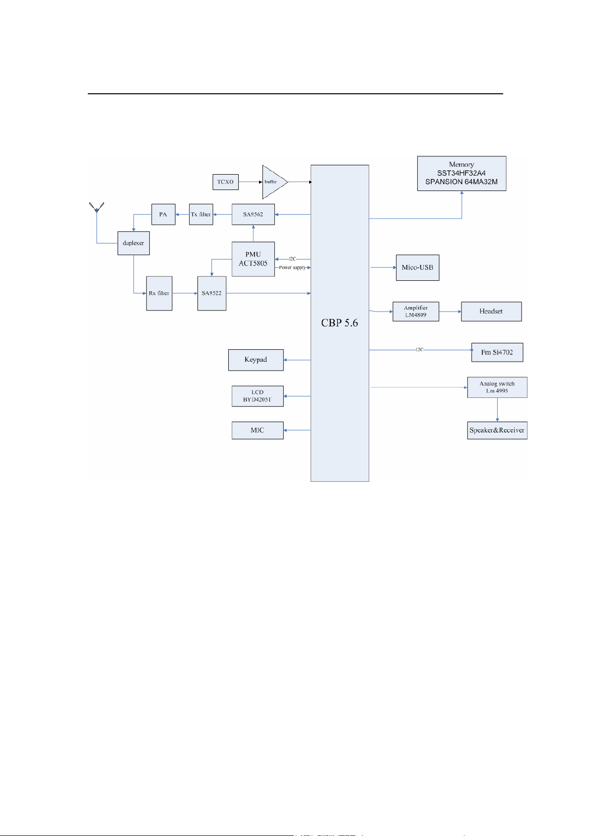
System Block Diagram
System Description
1508i is a CDMA (PCS band) Mobile Phone. The phone supports:
- forward and reverse link data rates of up to 153.6kbps.
- 4GV vocoder
- 1.47”(128*128) CSTN LCD
- Stereo FM radio
Platform Introductions
CBP 5.6
VIA Telecom’s CBP 5.6 single-chip CDMA Base Band
Processors provide a complete 3G CDMA2000® 1X
(Release 0) solution. They are designed to meet or exceed
Issue 1
Copyright © 2008 Nokia, All rights reserved
Page 6

1508i(RM-430)
Baseband Description and Troubleshooting
Nokia Customer
Care
the specifications of mobile stations for worldwide 3G CDMA
systems as specified by CDMA2000® 1X (Release 0)
standards and are backward-compatible to IS -95.
CBP 5.6 integrates three processor subsystems:
ARM7TDMI® Control Processor (CP) supports the protocol
stack, user interface, and hardware interface processing.
Two TeakLite® Digital Signal Processors (DSPs): one DSP
supports CDMA modem processing, the second DSP
supports CDMA voice processing
The main features of the CBP 5.6
z Supports CDMA2000® 1X (Release 0)
z Backward compatible to IS-95 standards
z Supports IS-2000 Quick Paging Channel for improved standby time
z Support for multiple CDMA band classes (Band Class 0/US-Cellular,
Band Class 1/US-PCS, Band Class 3/JTACS, Band Class 4/KoreanPCS); support for additional band classes which can be added upon
customer request
z Special purpose logic provides signal processing, modulation,
demodulation, hardware accelerators and interfaces for keypad and
display
z Mixed signal circuitry for the Rx analog-to-digital converter (ADC), Rx
filter, Tx digital-to-analog converter (DAC), Tx filter, internal PLLs,
voice codec, auxiliary ADCs, auxiliary DACs, RF control and 32.768
kHz oscillator
z Support for forward and reverse link data rates of up to 153.6 kbps
(CBP5.6 only).
z
Dual supply voltage (1.8 V digital core, 3.0 V analog and 3.0 V digital
I/O)
z 3.0 V or 1.8 V external memory interface
Issue 1
Copyright © 2008 Nokia, All rights reserved
Page 7

1508i(RM-430)
Baseband Description and Troubleshooting
Nokia Customer
Care
z USB support (12 Mbps)
z Removable User Identity Module (R-UIM) compliant with IS-820
z 32-voice polyphonic ringer
Issue 1
Copyright © 2008 Nokia, All rights reserved
Page 8

1508i(RM-430)
Baseband Description and Troubleshooting
Nokia Customer
Care
The interface of the CBP5.6 is described in the following
diagram. Receive and transmit interfaces for CBP 5.6
provide analog I and Q signals and support superheterodyne radio and direct conversion radio design. The
CP external-memory interface supports 3.0V or 1.8V, the
address bus supports 16-bit address which can support
three to six external devices via chip selects. CBP 5.6
includes 48 GPIOs and interrupts, some of which are
multiplexed with other functions. All GPIO pins are in input
state by default and use a large pull-up or pull-down resistor
value to minimize the current drain. The USB port supports
data rates of up to 12Mbps, the USB analog drivers and
48.00MHz PLL are integrated into CBP 5.6, the control
processor manages the USB function. Two independent
serial-peripheral interfaces are provided on CBP 5.6: one is
for RF control and the other is for general-purpose use. The
R-UIM interface supports 3V UIM cards and consists of five
pins, these pins are multiplexed with another function. The
CP manages the R-UIM function.
Five independent PDM DACs are supplied on the CBP 5.6
chip.
Three of the outputs are dedicated to radio-control signals
for Rx automatic gain control (AGC), Tx AGC, and automatic
frequency control (AFC). The fourth and fifth PDM outputs
are spares. The PDMs are 12-bit DACs and have a
guaranteed output range of 0.2 V to 2.5 V.
The 12-bit auxiliary ADC supports eight independent
external channels on pins AUXADC [7:0]. There are also
eight internal channels used to measure internal analog
voltages. The input voltage range is 0.2 V to 2.7 V. The
conversion time is 156 µsec. The typical uses of the external
Issue 1
Copyright © 2008 Nokia, All rights reserved
Page 9
1508i(RM-430)
Baseband Description and Troubleshooting
Nokia Customer
Care
auxiliary ADC channels include: Tx RF power measurement,
battery voltage, and temperature sensors.
The baseband is powered by the following PMU ACT5805 regulators:
VDD_DIG = 3.0v
VDD_CORE = 1.8v
VDD_TXPLL = 3.0v
VDD_TCXO = 3.0v
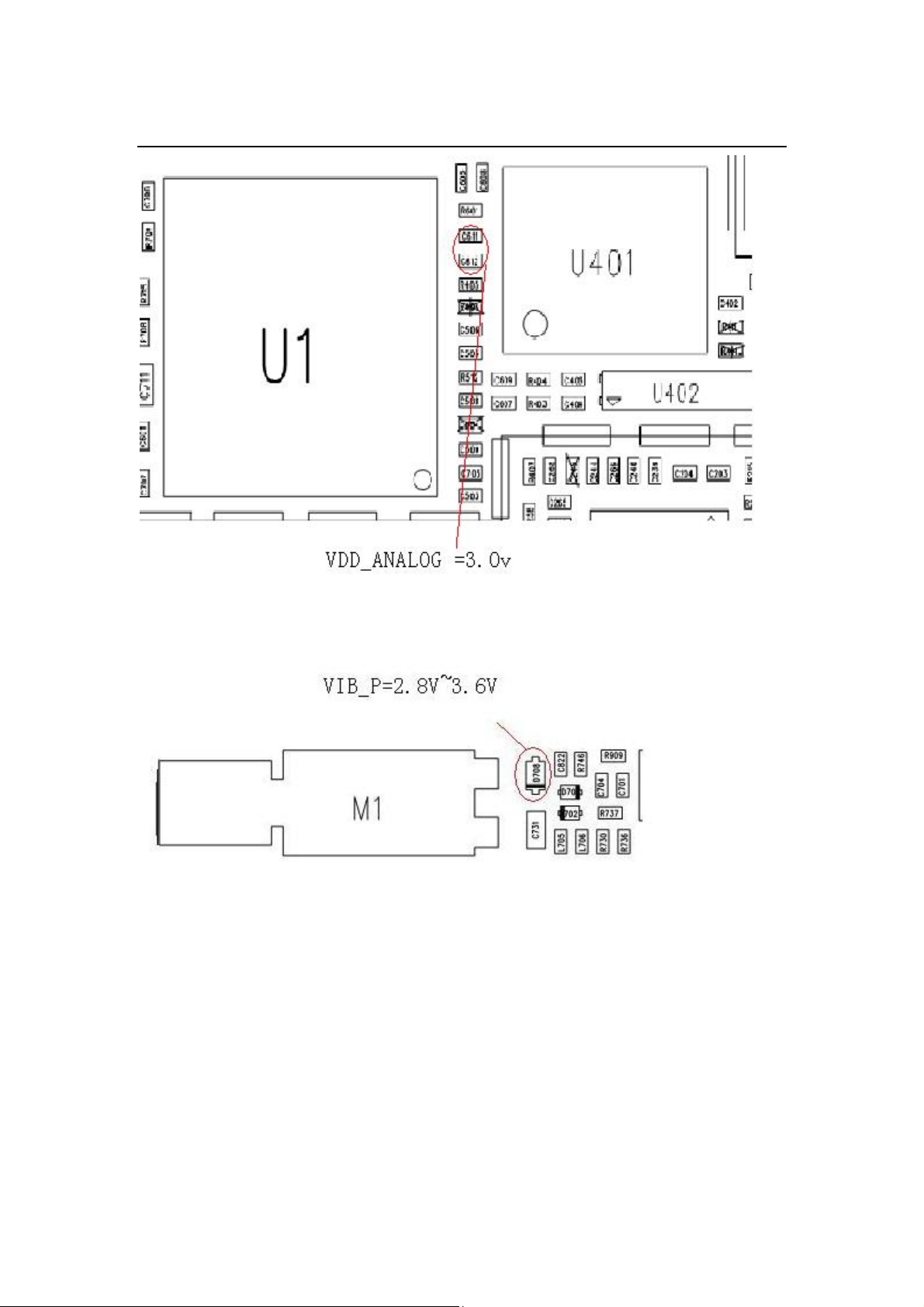
VDD_ANALOG =3.0v
VDD_RX = 3.0v
VDD_TX = 3.0v
VIB_P=2.8v~3.6v
Issue 1
Copyright © 2008 Nokia, All rights reserved
Page 10
1508i(RM-430)
Baseband Description and Troubleshooting
Nokia Customer
Care
Power Up
The mobile terminal uses the power key and a charger to power up.
Power Key
When the power key is pressed, the PMU enters the power-up sequence.
Pressing the power key causes the POWER_ON pin to VBAT. The
POWER_ON signal is not part of the keypad matrix. The power key is
connected to the PMU. This means that when the power key is pressed, an
interrupt will be generated to the CBP in order to power on the CBP. The CBP
Issue 1
Copyright © 2008 Nokia, All rights reserved
Page 11

1508i(RM-430)
Baseband Description and Troubleshooting
Nokia Customer
Care
reads the PMU IC’s interrupt register and notifies that it is a KPADPWR_N
interrupt. The CBP reads the status of the POWER_ON signal using the
PMU’s (I2C) control bus. If the POWER_ON signal stays High for a certain
time, the CBP accepts this as a valid power-on state and continues with the
software baseband initialization. If the power key does not indicate a valid
power-on situation, the CBP powers off the baseband
.
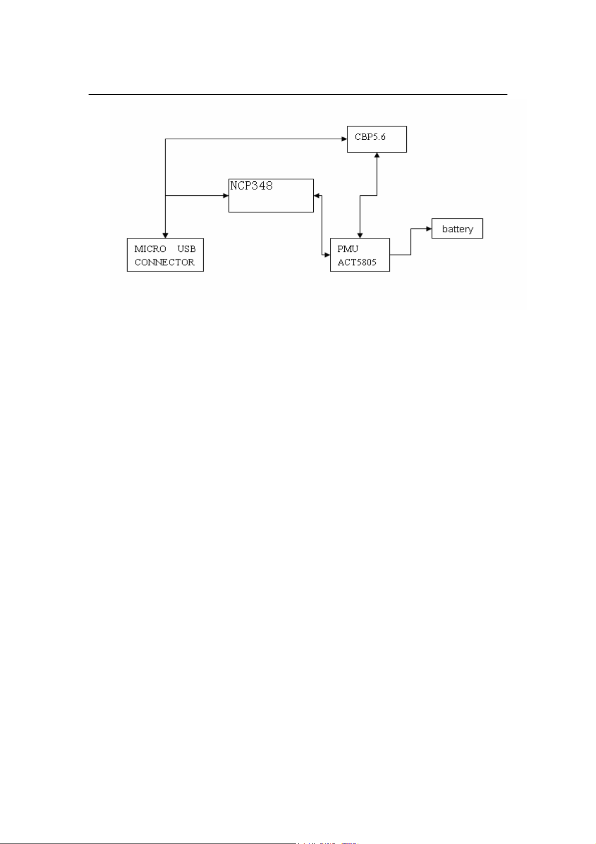
Charger
Charging is controlled by start-up charging circuitry in order to detec t and s tart
charging in case the main battery is not full and the PMU has no supply.
Power Off
While the PS_HOLD signal from the CBP is high, and the PMU IC is in
power-on status. The PMU continually monitors three events that could
trigger a power-off sequence:
z The CBP drives the PS_HOLD signal low responding to the pressing
of the keypad power button.
z Battery voltage drops below power off threshold (Battery Voltage <
3.2V).
z The PMU IC die temperature exceeds its “severe” over-temperature
threshold.
Power Distribution
In normal operation, the baseband is powered by the mobile terminal‘s
battery pack. The battery pack consists of one lithium-ion cell with a
capacity of 860 mA and safety and protection circuits.
The PMU ACT5805 IC controls the power distribution for the whole mobile
terminal, which includes the baseband and the RF regulators, but excludes
the RF power amplifier (RF PA) which drains power from the battery
Issue 1
Copyright © 2008 Nokia, All rights reserved
Page 12

1508i(RM-430)
Baseband Description and Troubleshooting
Nokia Customer
Care
directly. The battery provides power directly to the following parts of the
system:
· PMU ACT5805
· RF PA
· Vibrator
· Keyboard & LCD backlights
· Audio Amplifier
The heart of the power distribution is the power control block inside the
PMU ACT5805. It includes all the voltage regulators and feeds the power
to the entire system. The PMU ACT5805 handles hardware power-up
functions so that the regulators are not powered on and the power up reset
(NRST) is not released if the battery voltage is less than 3.2 V.
The baseband is powered by the following PMU ACT5805 regulators:
Rating
Regulator Voltage
Notes
Current
Always enabled except during
VDD_DIG 3V 250mA
power-off mode
Enabled only when the system is
VDD_CORE 1.8V 150mA
powered on (Off during sleep and
power-off modes)
Enabled only when the
VDD_TXPLL 3.0V 80mA
transmitter is on
VDD_TCXO 3.0V 80mA
KEYPAD_LED 3.0V 100mA
Copyright © 2008 Nokia, All rights reserved
Enabled only when the system is
powered on (Off during sleep and
power-off modes)
Enabled when the system is
powered on, or the keys are
Issue 1
Page 13

1508i(RM-430)
Baseband Description and Troubleshooting
Nokia Customer
Care
pressed,etc.
VDD_RX 3.0V 80mA Enabled when the receiver is on
Enabled when the transmitter is
VDD_TX 3.0V 150mA
on
Enabled only when the system is
VDD_VIBE 3.0V 150mA
powered on (Off during sleep and
power-off modes)
Clock Distribution
The CBP derives its internal clock from two clock inputs, TCXO and
SLEEP_CLK.
The main clock signal for the baseband is generated from TCXO.
(Temperature-compensated crystal oscillator) The CBP’s TCXO clock
input supports the frequency 19.2 MHz +/-2ppm. An integrated PLL and
digital divider inside the CBP are used to create the required clock for the
system.
The SLEEP_CLK provides a 32.768 kHz +/-20ppm clock source to drive
the CBP controller into sleep mode. At this mode, the TCXO is disabled.
TCXO
The CBP device integrates a phase-locked loop from the TCXO clock
input.
The PMU optimizes TCXO operation that enables and disables
appropriate circuits in the proper sequence. The controller is enabled by
the OSC_EN signal from the CBP. .
SLEEP Crystal Circuit for 32.768 kHz
The 32.768 kHz crystal oscillator is the primary SLEEP clock source when TCXO
clocks are disabled to save power.
Issue 1
Copyright © 2008 Nokia, All rights reserved
Page 14

1508i(RM-430)
Baseband Description and Troubleshooting
Nokia Customer
Care
Charging Operation
Battery
The 1508i uses a Lithium-Ion cell battery with a capacity of 860mA.CBP
reads the resistor inside the battery pack on the BSI line to identify the
battery size. Different charging algorithm will be used for different battery
sizes. The resistors are connected to the BSI pin inside the battery
connector.
BSI= BATT_DET
Charging Circuitry
Issue 1
Copyright © 2008 Nokia, All rights reserved
Page 15
1508i(RM-430)
Baseband Description and Troubleshooting
Nokia Customer
Care
Display and Keypad
The mobile terminal uses light-emitting diodes (LEDs) for liquid crystal display
(LCD) and keypad illumination. There are two white LEDs for the LCD and two
LEDs for the keypad. KEYPAD_LED is the signal used to drive keypad LEDs.
LCD_BL_EN is the signal used to drive LCD LEDs. The mobile terminal uses a
color LCD. The interface uses a parallel bus to transfer the Command/ Data
between CBP and LCD.
Troubleshooting
First, carry out a thorough visual check of the module. Make sure in
particular that:
• There is no mechanical damage.
• Soldered joints are OK.
• ASIC orientations are OK.
The following hints should help find the cause of the problem when the
circuitry seems to be faulty. Troubleshooting instructions are divided into
the following sections:
Issue 1
Copyright © 2008 Nokia, All rights reserved
Page 16

1508i(RM-430)
Baseband Description and Troubleshooting
Nokia Customer
Care
·‘Power Does Not Stay ON’
·“Charger Faults’
·‘Audio Faults’
·‘Display Faults’
·‘Keypad Faults’
·‘No Vibration’
·‘Series/USB Interface Disabled’
·‘UIM Card Unreadable’
Note:
• CBP5.6 is underfilled and can not be replaced.
• The Shielding Case Assy can not be reused after removal.
• After using the heatgun, the domesheet needs to be replaced.
Issue 1
Copyright © 2008 Nokia, All rights reserved
Page 17

1508i(RM-430)
Baseband Description and Troubleshooting
Nokia Customer
Care
Repair Function in Power-off Status (refer to PMU Circuit)
• The current status resulting ‘Power Off” could be divided into three
cases:
• Big current, no current, no holding current.
Case One.
Big current appears when power is fed to Vbattery or “power on” key is
pressed on the handset.
Check if the following voltages of PMU are normal: VDD_DIG,
VDD_CORE, VDD_TXPLL, VDD_TCXO, VDD_RX, VDD_TX,
If the voltages are abnormal, check the fault reason.
Case Two.
If current is zero, check CN703and
C1011,C1012,C1013,C1014,C1015,C1016.If there is no power output,
PMU is defective. Phone cannot be repaired and must be replaced.
Case Three.
Raise the voltage of PS-HOLD, and measure every output voltage of PMU,
The reference clock Power-on needed is KHZ.19.2MHZ etc.
such
as :VDD_DIG,VDD_CORE,VDD_TXPLL,VDD_TCXO,VDD_RX,VDD_TX ;
Check if the clock TCXO(19.2MHz)and RTC(32.768KHz)are normal.
If the signals are abnormal, please check the fault reason;
If it is normal, please check the welding of CPU and Flash and perform
welding or replacement. (Replacement includes Flash Updating).The
welding of the display panel connector should also be checked, becaus e
the shortcut of the parallel data signal and Read & Write signal on the
display panel connector will lead to failure of CPU in invoking the
programs of FLASH.
Issue 1
Copyright © 2008 Nokia, All rights reserved
Page 18

1508i(RM-430)
Baseband Description and Troubleshooting
Nokia Customer
Care
Power Does Not Stay ON Troubleshooting
Issue 1
Copyright © 2008 Nokia, All rights reserved
Page 19

1508i(RM-430)
Baseband Description and Troubleshooting
Nokia Customer
Care
PMUACT5805 circuits
Issue 1
Copyright © 2008 Nokia, All rights reserved
Page 20

1508i(RM-430)
Baseband Description and Troubleshooting
Nokia Customer
Care
Issue 1
Copyright © 2008 Nokia, All rights reserved
Page 21

1508i(RM-430)
Baseband Description and Troubleshooting
Nokia Customer
Care
No Sound in Earpiece & Microphone Check (refer to MIC
headset, Audio PA Circuit design)
Enter the test mode ’LoopBack’ by pressing test order #0000# then press
‘calling key’ when the No Sound in Earpiece & Microphone message
appears.
1. If the test result is normal, it indicates that the ‘Loopback’ circuit
(receiver & microphone) is OK in hardware connection; The bottom
socket should be checked whether it has been short circuited to the
ground; If it is grounded, the mobile phone software will detect that the
earpiece is in the Insert Mode, which sets the mobile phone in earpiece
mode, and it means both of the earpiece and the microphone do not work.
2. On the Other hand, if the test result shows that the ‘Loopback’ is
abnormal, the fault reason should be picked up from the earpiece and the
microphone. Dial 112 emergency call and diagnose the fault:
If the sound works, the microphone Mic is directed wrong, or it indicates
the receiver does not work properly.
3. In the case the Contact Connection is adopted between the earpiece
and the Mic of the mobile phone, test if the connection works.
• If there is a fault in telephone receiver, first try to recover the earpiece
by performing the experiment described above. If it still doesn’t work,
Audio PA chip or CPU chips may be damaged from poor welding or
injury. The chips then should be repaired by re-welding or replacement.
• If there is a fault in Microphone, first try to recover the earpiece by
performing the experiment described above. If it still doesn’t work,
Audio PA chip or CPU chips maybe damaged from poor welding or
injury. The chips then should be repaired by re-welding or replacement.
Issue 1
Copyright © 2008 Nokia, All rights reserved
Page 22

1508i(RM-430)
Baseband Description and Troubleshooting
Nokia Customer
Care
Audio Faults Troubleshooting
Issue 1
Copyright © 2008 Nokia, All rights reserved
Page 23

1508i(RM-430)
Baseband Description and Troubleshooting
Nokia Customer
Care
Issue 1
Copyright © 2008 Nokia, All rights reserved
Page 24

1508i(RM-430)
Baseband Description and Troubleshooting
Nokia Customer
Care
MIC Circuit Design
Headset Circuitry
Issue 1
Copyright © 2008 Nokia, All rights reserved
Page 25

1508i(RM-430)
Baseband Description and Troubleshooting
Nokia Customer
Care
Audio PA Circuitry
Display Faults
Display fault items are listed as following: white panel, backlight N/G, display
flowery or color abnormal. First check if the LCD is well connected with the LCD,
if not well connected or poor welding, replace the connection or weld it again. If
the connection is good, the data input on LCD and its operation voltage should
be checked. If the results show poor condition, then find the fault reason and do
the replacement and double welding. More attention should be payed on CPU
cold welding.
Issue 1
Copyright © 2008 Nokia, All rights reserved
Page 26

1508i(RM-430)
Baseband Description and Troubleshooting
Nokia Customer
Care
Display Faults Troubleshooting
Issue 1
Copyright © 2008 Nokia, All rights reserved
Page 27

1508i(RM-430)
Baseband Description and Troubleshooting
Nokia Customer
Care
Keypad Faults (refer to Keypad circuitry)
First check if the keypad is well located: If not, locate it again or do the
replacement.
Find out if there are faulty keys. Illustrated by the interface circuit of the
Keypad, except the PHONE-ON Key which is connected to the PMU
Chip separately , all the keys work in groups(R0 to R5 and C0 to C3)
and each group use one CPU’s GPIO. Thus the faulty running GPIO
can be located by confirming the faulty keys. Further, short circuited
signal or cold welding of the CPU should be modified or replaced.
Issue 1
Copyright © 2008 Nokia, All rights reserved
Page 28

1508i(RM-430)
Baseband Description and Troubleshooting
Nokia Customer
Care
Keypad Faults Troubleshooting
Issue 1
Copyright © 2008 Nokia, All rights reserved
Page 29

1508i(RM-430)
Baseband Description and Troubleshooting
Keypad Circuitry
Nokia Customer
Care
Vibrator Faulty reference to the Vibrator Circuit Design)
First check whether the vibrator is connected well with the PWB.
Set the digital power at 3.0V (The voltage value may be changed by model of the
vibrator). The Power should fall on the two control points of the vibrator, and then
observe whether it works. If the Vibrator does not work, please do the replacement;
If the vibrator works, which means no control signal arrivals, do the check against he
current’s flow.
In addition, No Vibration after installation usually dedicates the welding
excursion of the vibration. Check with it and see if it has been connected
properly.
Issue 1
Copyright © 2008 Nokia, All rights reserved
Page 30

1508i(RM-430)
Baseband Description and Troubleshooting
Nokia Customer
Care
No Vibration Troubleshooting
Vibrator Circuit
Issue 1
Copyright © 2008 Nokia, All rights reserved
Page 31

1508i(RM-430)
Baseband Description and Troubleshooting
Nokia Customer
Care
C
hecking Series
1. Check if the bottom insert of the mobile phone is well connected.
2. Check if the COM of the computer is well connected.
And confirm the configuration of the COM setting.
3. Check the welding of the mobile phone connection, whether there is
foreign impurity or not.
4. Check if the Rx, TX, DTR and etc. are shortcircuited to the ground.
5. Check the welding of the CPU.
Series Interface Disabled Troubleshooting
Checking USB
6. Check if the bottom insert of the mobile phone is well connected.
7. Check if the COM of the computer is well connected and confirm the
configuration of the COM setting.
Issue 1
Copyright © 2008 Nokia, All rights reserved
Page 32

1508i(RM-430)
Baseband Description and Troubleshooting
Nokia Customer
Care
8. Check the welding of the mobile phone connection, whether there is
foreign impurity
9. Check if the VBUS, D+, D- and etc. are in their normal status.
10. Check if the USB over-Voltage IC works normally.
11. Check the welding of the CPU.
USB Interface Disabled Troubleshooting
Issue 1
Copyright © 2008 Nokia, All rights reserved
Page 33

1508i(RM-430)
Baseband Description and Troubleshooting
Nokia Customer
Care
USB Circuitry
Issue 1
Copyright © 2008 Nokia, All rights reserved
Page 34

1508i(RM-430)
Baseband Description and Troubleshooting
Nokia Customer
Care
FM Faults Troubleshooting
Issue 1
Copyright © 2008 Nokia, All rights reserved
Page 35

1508i(RM-430)
Baseband Description and Troubleshooting
Nokia Customer
Care
UIM Card Unreadable troubleshooting
Issue 1
Copyright © 2008 Nokia, All rights reserved
Page 36

1508i(RM-430)
Baseband Description and Troubleshooting
Nokia Customer
Care
Charging Faults Troubleshooting
Issue 1
Copyright © 2008 Nokia, All rights reserved
Page 37

1508i(RM-430)
Baseband Description and Troubleshooting
Nokia Customer
Care
Issue 1
Copyright © 2008 Nokia, All rights reserved
 Loading...