

Page 1

Nokia Customer Care
Service Manual
RH-128 (Nokia 1506 ; L3&4)
Mobile Terminal
Part No: (Issue 1)
COMPANY CONFIDENTIAL
Copyright © 2009 Nokia. All rights reserved.
Page 2

Amendment Record Sheet
Amendment No Date Inserted by Comments
Issue 1 December, 2009 Lijun Gu
RH-128
Amendment Record Sheet
ii
COMPANY CONFIDENTIAL
Issue 1
Copyright © 2009 Nokia. All rights reserved.
Page 3

RH-128
Copyright
Copyright
Copyright© 2009 Nokia. All rights reserved.
Reproduction, transfer, distribution or storage of part or all of the contents in this document in any form without
the prior written permission of Nokia is prohibited.
Nokia, Nokia Connecting People, X and Y are trademarks or registered trademarks of Nokia Corporation. Other
product and company names mentioned herein may be trademarks or tradenames of their respective owners.
Nokia operates a policy of continuous development. Nokia reserves the right to make changes and
improvements to any of the products described in this document without prior notice.
Under no circumstances shall Nokia be responsible for any loss of data or income or any special, incidental,
consequential or indirect damages howsoever caused.
The contents of this document are provided "as is". Except as required by applicable law, no warranties of any
kind, either express or implied, including, but not limited to, the implied warranties of merchantability and fitness
for a particular purpose, are made in relation to the accuracy, reliability or contents of this document. Nokia
reserves the right to revise this document or withdraw it at any time without prior notice.
The availability of particular products may vary by region.
IMPORTANT
This document is intended for use by qualified service personnel only.
Issue 1
Copyright © 2009 Nokia. All rights reserved.
COMPANY CONFIDENTIAL
iii
Page 4

RH-128
Warnings and cautions
Warnings and cautions
Please refer to the phone’s user guide for instructions relating to operation, care and maintenance including
important safety information. Note also the following:
WARNINGS
z CARE MUST BE TAKEN ON INSTALLATION IN VEHICLES FITTED WITH ELECTRONIC ENGINE
MANAGEMENT SYSTEMS AND ANTI–SKID BRAKING SYSTEMS. UNDER CERTAIN FAULT
CONDITIONS, EMITTED RF ENERGY CAN AFFECT THEIR OPERATION. IF NECESSARY, CONSULT
THE VEHICLE DEALER/MANUFACTURER TO DETERMINE THE IMMUNITY OF VEHICLE
ELECTRONIC SYSTEMS TO RF ENERGY.
z THE HANDPORTABLE TELEPHONE MUST NOT BE OPERATED IN AREAS LIKELY TO CONTAIN
POTENTIALLY EXPLOSIVE ATMOSPHERES, EG PETROL STATIONS (SERVICE STATIONS),
BLASTING AREAS ETC.
z OPERATION OF ANY RADIO TRANSMITTING EQUIPMENT, INCLUDING CELLULAR TELEPHONES,
MAY INTERFERE WITH THE FUNCTIONALITY OF INADEQUATELY PROTECTED MEDICAL DEVICES.
CONSULT A PHYSICIAN OR THE MANUFACTURER OF THE MEDICAL DEVICE IF YOU HAVE ANY
QUESTIONS. OTHER ELECTRONIC EQUIPMENT MAY ALSO BE SUBJECT TO INTERFERENCE.
CAUTIONS
z Servicing and alignment must be undertaken by qualified personnel only.
z Ensure that all work is carried out at in anti–static workstation and that an anti–static wrist strap is worn.
z Use only approved components as specified in the parts list.
z Ensure that all components, modules screws and insulators are correctly re–fitted after servicing and
alignment.
z Ensure that all cables and wires are correctly repositioned.
iv
COMPANY CONFIDENTIAL
Issue 1
Copyright © 2009 Nokia. All rights reserved.
Page 5

RH-128
For your safety
For your safety
QUALIFIED SERVICE
Only qualified personnel may install or repair mobile terminal equipment.
ACCESSORIES AND BATTERIES
Use only approved accessories and batteries. Do not connect incompatible products.
CONNECTING TO OTHER DEVICES
When connecting to any other device, read its user’s guide for detailed safety instructions. Do not connect
incompatible products.
Issue 1
COMPANY CONFIDENTIAL
v
Copyright © 2009 Nokia. All rights reserved.
Page 6

ESD protection
RH-128
ESD protection
Nokia requires that product service points have sufficient ESD protection (against
static electricity) when servicing products.
Any product of which the covers are removed must be handled with ESD protection.
The SIM card can be replaced without ESD protection if the product is otherwise
ready for use.
To replace the covers ESD protection must be applied.
All electronic parts of the product are susceptible to ESD. Resistors, too, can be
damaged by static electricity discharge.
All ESD sensitive parts must be packed in metallized protective bags during
shipping and handling outside any ESD Protected Area (EPA).
Every repair action involving opening the product or handling the product
components must be done under ESD protection.
ESD protected spare part packages MUST NOT be opened/closed out of an ESD
Protected Area.
For more information and local requirements about ESD protection and ESD
Protected Area, contact your local Nokia After Market Services representative.
vi
Copyright © 2009 Nokia. All rights reserved.
COMPANY CONFIDENTIAL
Issue 1
Page 7

RH-128
Care and maintenance
Care and maintenance
This product is of superior design and craftsmanship and should be treated with care. The suggestions
below will help you to fulfill any warranty obligations and to enjoy this product for many years.
Keep the phone and all its parts and accessories out of the reach of small children.
Keep the phone dry. Precipitation, humidity and all types of liquids or moisture can contain minerals that will
corrode electronic circuits.
Do not use or store the phone in dusty, dirty areas. Its moving parts can be damaged.
Do not store the phone in hot areas. High temperatures can shorten the life of electronic devices, damage
batteries, and warp or melt certain plastics.
Do not store the phone in cold areas. When it warms up (to its normal temperature), moisture can form
inside, which may damage electronic circuit boards.
Do not drop, knock or shake the phone. Rough handling can break internal circuit boards.
Do not use harsh chemicals, cleaning solvents, or strong detergents to clean the phone.
Do not paint the phone. Paint can clog the moving parts and prevent proper operation.
Use only the supplied or an approved replacement antenna. Unauthorized antennas, modifications or
attachments could damage the phone and may violate regulations governing radio devices.
All of the above suggestions apply equally to the product, battery, charger or any accessory.
Issue 1
COMPANY CONFIDENTIAL
Copyright © 2009 Nokia. All rights reserved.
vii
Page 8

RH-128
Company policy
Company policy
Our policy is of continuous development; details of all technical modifications will be included with service
bulletins.
While every endeavor has been made to ensure the accuracy of this document, some errors may exist. If
any errors are found by the reader, NOKIA MOBILE PHONES Business Group should be notified in writing.
Please state:
Title of the Document + Issue Number/Date of publication
Latest Amendment Number (if applicable)
Page(s) and/or Figure(s) in error
Please send to:
NOKIA CORPORATION
Nokia Mobile Phones Business Group
Nokia Customer Care
PO Box 86
FIN-24101 SALO
Finland
viii
Copyright © 2009 Nokia. All rights reserved.
COMPANY CONFIDENTIAL
Issue 1
Page 9

RH-128
Battery information
Battery information
Note that a new battery's full performance is achieved only after two or three complete charge and
discharge cycles!
The battery can be charged and discharged hundreds of times but it will eventually wear out. When the
operating time (talk-time and standby time) is noticeably shorter than normal, it is time to buy a new battery.
Use only batteries approved by the phone manufacturer and recharge the battery only with the chargers
approved by the manufacturer. Unplug the charger when not in use. Do not leave the battery connected to a
charger for longer than a week, since overcharging may shorten its lifetime. If left unused a fully charged
battery will discharge itself over time.
Temperature extremes can affect the ability of your battery to charge.
For good operation times with Ni-Cd/NiMh batteries, discharge the battery from time to time by leaving the
product switched on until it turns itself off (or by using the battery discharge facility of any approved
accessory available for the product). Do not attempt to discharge the battery by any other means.
Use the battery only for its intended purpose.
Never use any charger or battery that is damaged.
Do not short-circuit the battery. Accidental short-circuiting can occur when a metallic object (coin, clip or pen)
causes direct connection of the + and – terminals of the battery (metal strips on the battery) for example
when you carry a spare battery in your pocket or purse. Short-circuiting the terminals may damage the
battery or the connecting object.
Leaving the battery in hot or cold places, such as in a closed car in summer or winter conditions, will reduce
the capacity and lifetime of the battery. Always try to keep the battery between 15°C and 25°C (59°F and
77°F). A phone with a hot or cold battery may temporarily not work, even when the battery is fully charged.
Batteries' performance is particularly limited in temperatures well below freezing.
Do not dispose of batteries in a fire!
Dispose of batteries according to local regulations (e.g. recycling). Do not dispose as household waste.
Issue 1
COMPANY CONFIDENTIAL
ix
Copyright © 2009 Nokia. All rights reserved.
Page 10

RH-128
Battery information
(This page left intentionally blank.)
x
COMPANY CONFIDENTIAL
Issue 1
Copyright © 2009 Nokia. All rights reserved.
Page 11

RH-128
Nokia 1506; L3&4 Service Manual Structure
Nokia 1506; L3&4 Service Manual Structure
1- General Information
2- Service Software Instruction
3- Service Tools
4- Antenna Description and Troubleshooting
5- Baseband Description and Troubleshooting
6- RF Description and Troubleshooting
7- Schematics
Glossary
Issue 1
COMPANY CO NFIDENTIA L
xi
Copyright © 2009 Nokia. All rights reserved.
Page 12

RH-128
Nokia 1506; L3&4 Service Manual Structure
(This page left intentionally blank.)
xii
COMPANY CO NFIDENTIA L
Issue 1
Copyright © 2009 Nokia. All rights reserved.
Page 13

Nokia Customer Care
1- General Information
Issue 1
Copyright © 2009 Nokia. All rights reserved.
COMPANY CONFIDENTIAL
Page 1-1
Page 14

RH-128
General Information
(This page left intentionally blank.)
COMPANY CONFIDENTIAL
Copyright © 2009 Nokia. All rights reserved.
Issue 1 Page 1-2
Page 15

RH-128
General Information
Table of Contents
Product selection....................................................................................................................page 1-5
RH-128 PCI overview...............................................................................................................page 1-6
Phone features and sales package..........................................................................................page 1-7
Accessories............................................................................................................................page 1-8
Technical Specifications..........................................................................................................page 1-8
General specifications.....................................................................................................page 1-8
Battery endurance...........................................................................................................page 1-9
COMPANY CONFIDENTIAL
Copyright © 2009 Nokia. All rights reserved.
Page 1-3 Issue 1
Page 16

RH-128
General Information
(This page left intentionally blank.)
COMPANY CONFIDENTIAL
Copyright © 2009 Nokia. All rights reserved.
Issue 1 Page 1-4
Page 17
RH-128
General Information
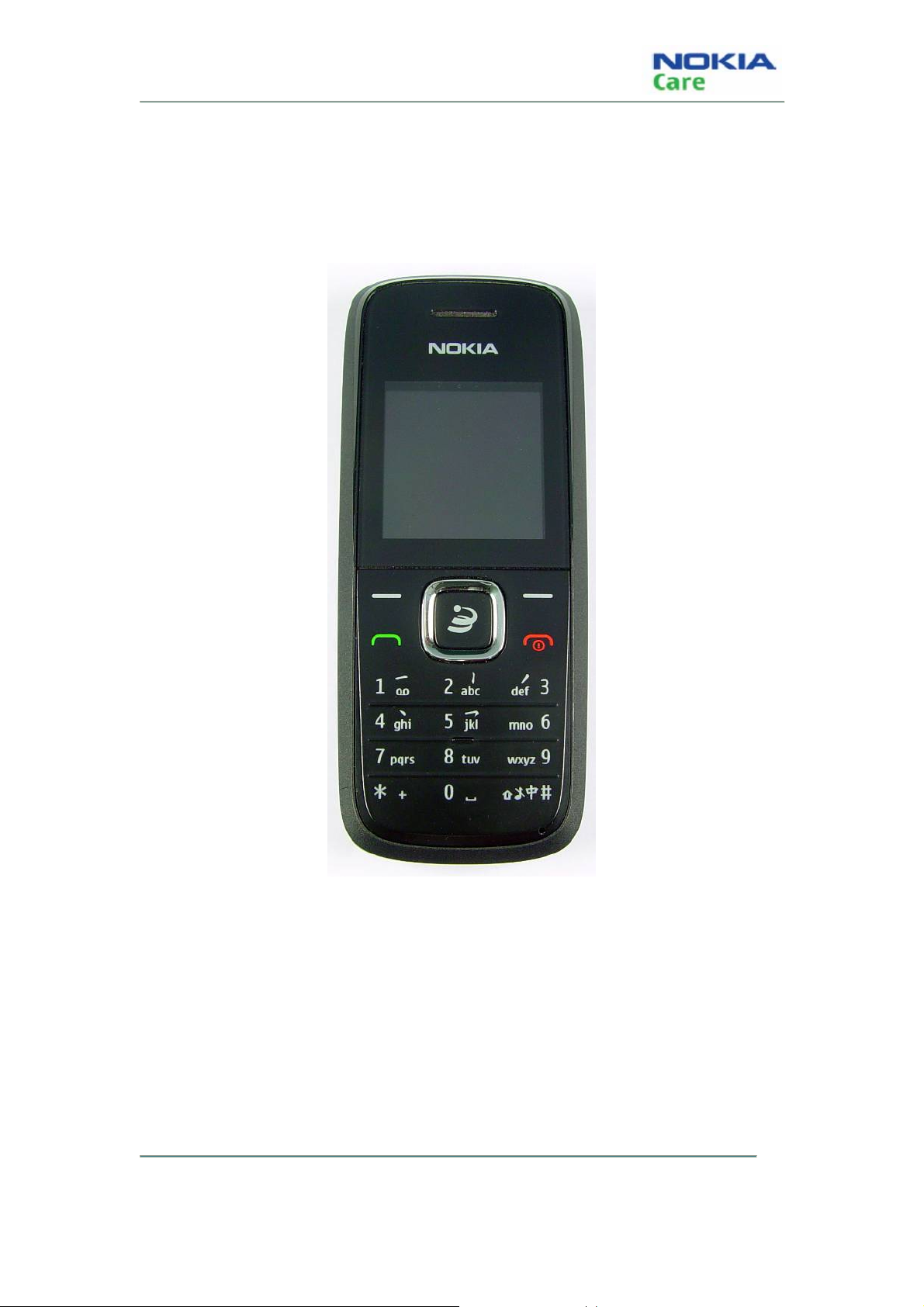
Product selection
RH-128 (Nokia 1506) mobile terminal offers a CDMA single band engine.
Figure 1: View of RH-128
COMPANY CONFIDENTIAL
Copyright © 2009 Nokia. All rights reserved.
Page 1-5 Issue 1
Page 18
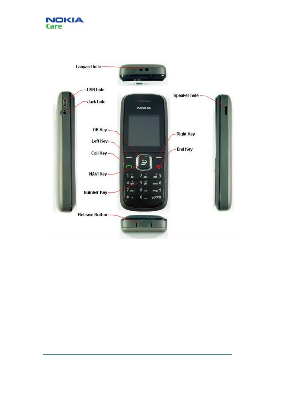
RH-128 PCI overview
RH-128
General Information
COMPANY CONFIDENTIAL
Copyright © 2009 Nokia. All rights reserved.
Issue 1 Page 1-6
Page 19

RH-128
General Information
Phone features and sales package
Hardware & Mechanics
z 800MHz, CDMA2000 1xRTT
z 1.47” 128*128 CSTN, 65k Main display
z 4-way Navigation Keys
z Internal antenna
z IHF speaker
z Battery (860mAh, BL-4C)
z RUIM
z 4-pin 2.5mm audio jack required for UHJ support
z Micro-USB 2.0
z White Backlighting
z Lanyard notch/ hole
SW
z Long SMS just for China telecom version
z SMS with predictive text
z Calling Restrictions
z 32midi ring tone
z Minimum 500 contacts with 5 phone entries per name
z Access to Voice Mail
z Alarm Clock, Calculator, Calendar, Timer, World Clock
z Voice Memo recording (at least 90 seconds)
z MSL/SPC supported
z OTAPA/OTASP supported
z Airplane Mode supported
z OMSI Interface supported
z Support for GIF, JPG, PNG image formats and BMP image formats
COMPANY CONFIDENTIAL
Copyright © 2009 Nokia. All rights reserved.
Page 1-7 Issue 1
Page 20

z 5 pre-loaded alarm tones and 20 Ring tones pre-installed
Sales package contents
z Transceiver: RH-128
z Standard Battery (860 mAh Li-on): BL-4C
z AC-6C/AC-8C
z User Guide
Accessories
Supported accessories
Type Name
RH-128
General Information
DC-6 Car Charger
AC-6C Travel Charger
DT-28 Charging Deskstand
WH-101 Stereo Headset
WH-100 2.5mm Mono headset
CA-101 Micro USB Cable
Technical Specifications
General specifications
Unit Dimension (mm) Weight (g) Volume (cc)
Transceiver with
103.8*43*15.4 70 56
BL-4C; 860 mAh Li-Ion
battery pack
COMPANY CONFIDENTIAL
Copyright © 2009 Nokia. All rights reserved.
Issue 1 Page 1-8
Page 21

RH-128
General Information
Battery endurance
Battery Talk Time Standby Time
BL-4C 860 mAh Li-ion 3.25 hours China 2 to 10 days
SEAP/MEA/LTA 4 to 10 days
COMPANY CONFIDENTIAL
Page 1-9 Issue 1
Copyright © 2009 Nokia. All rights reserved.
Page 22

RH-128
General Information
(This page left intentionally blank.)
COMPANY CONFIDENTIAL
Copyright © 2009 Nokia. All rights reserved.
Issue 1 Page 1-10
Page 23

Nokia Customer Care
2- Service Software Instructions
COMPANY CONFIDENTIAL
Copyright © 2009 Nokia. All rights reserved.
Page 2-1 Issue 1
Page 24

RH-128
Service Software Instruction
(This page left intentionally blank.)
COMPANY CONFIDENTIAL
Copyright © 2009 Nokia. All rights reserved.
Issue 1 Page 2-2
Page 25

RH-128
Service Software Instruction
Table of Contents
Software summary..............................................................................................................................page 2-5
Hardware, Operating system and environment request.........................................................page 2-5
Software utilization....................................................................................................................page 2-5
Installation..................................................................................................................................page 2-5
Use of AMS..........................................................................................................................................page 2-8
Download Mode........................................................................................................................page 2-11
General Mode ...........................................................................................................................page 2-16
Issue 1 Page 2-3
COMPANY CONFIDENTIAL
Copyright © 2009 Nokia. All rights reserved.
Page 26

RH-128
Service Software Instruction
(This page left intentionally blank.)
COMPANY CONFIDENTIAL
Copyright © 2009 Nokia. All rights reserved.
Issue 1 Page 2-4
Page 27
RH-128
Service Software Instruction
Software summary
In order to understand the requests of operating device and driver for the software, the user should read
this chapter carefully before using Nokia 1508 AMS tool. Users can setup the PC according to their own
needs, in order to get the most out of the service software.
Hardware, Operating system and environment request
Table.1 shows the lowest request for Hardware configuration.
Operating system: Windows 2000, Windows XP
PC Minimum Requirement
Processor 700MHz
RAM 256MB
Required Disk space 100MB
Interface ports USB
Table.1 Lowest request for Hardware configuration
Software utilization
Insert Dongle.
AMS has two function modes: Download mode and General mode. When in download mode, the
handset must be working in this mode. When in general mode, the handset must be working in power
up mode. AMS tool will report Warning message if the two modes are used incorrectly.
Download mode comprises of one type: Emergency Download. General mode includes six types:
Phone Information, Display Capture, Label Print, Critical Data Backup, RF Calibration and RF Tool.
Installation
Please install the Nokia 1506 AMS tool as follows. It generally has three parts, where driver and RF Tool
Run Time must be installed separately. You can install the AMS software directly if the driver and RF
Tool Run Time are already installed.
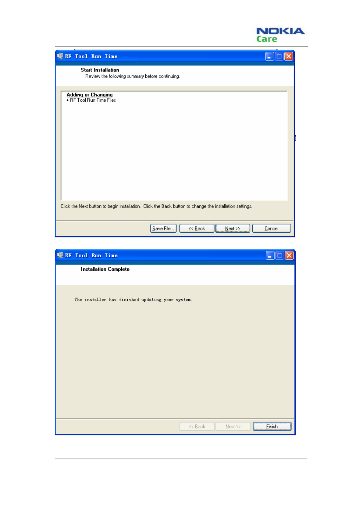
Steps for installing RF Tool Run Time:
1. Double click the setup.exe,
2. It will remind you to select the installation path. Click “next” to continue with the following steps.
Issue 1 Page 2-5
COMPANY CONFIDENTIAL
Copyright © 2009 Nokia. All rights reserved.
Page 28
RH-128
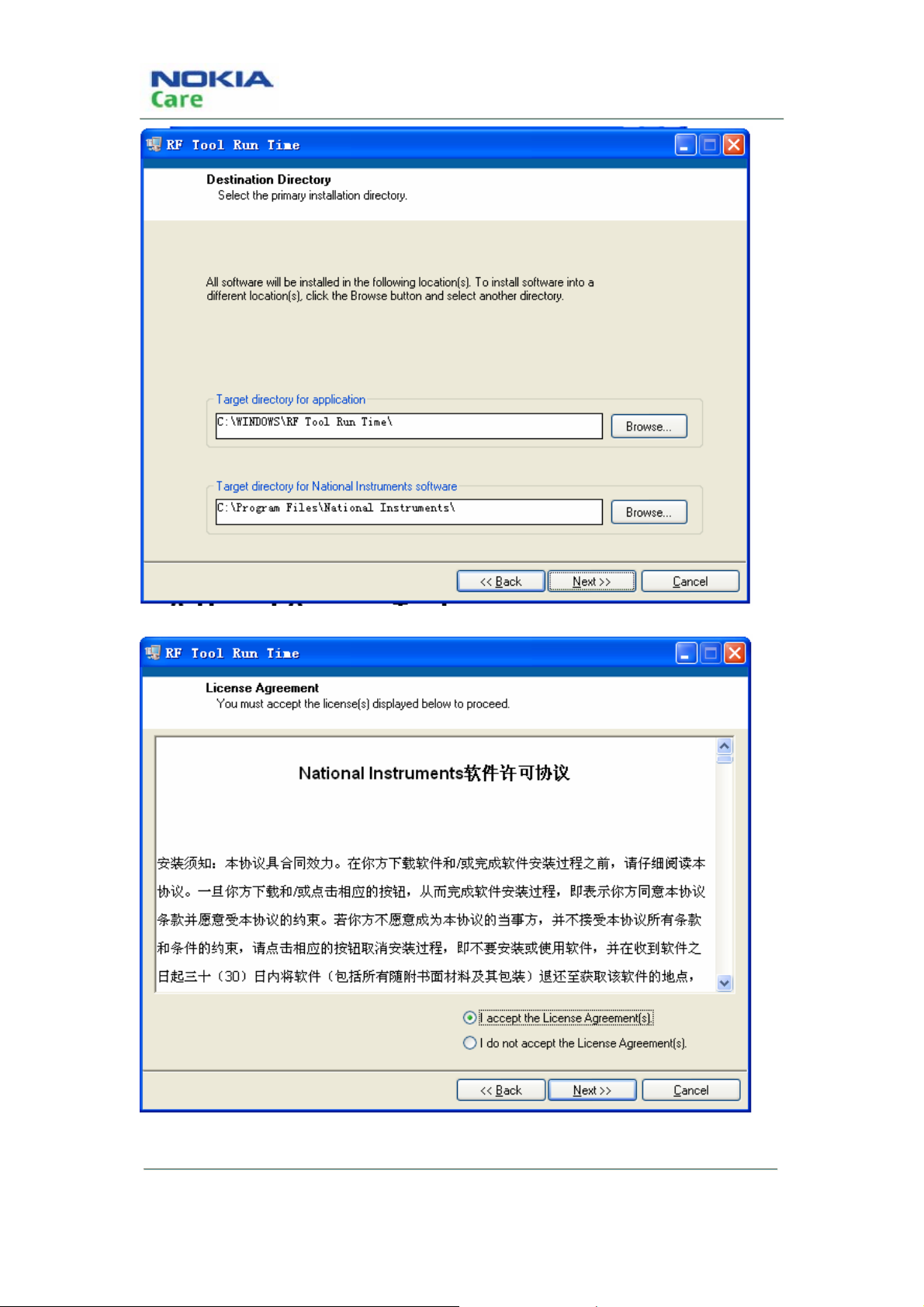
Service Software Instruction
3. Select “I accept the License Agreement(s)”. Then click “Next”.
4. Click “Next”.
COMPANY CONFIDENTIAL
Copyright © 2009 Nokia. All rights reserved.
Issue 1 Page 2-6
Page 29
RH-128
Service Software Instruction
5. Click “Finish” button to complete the installation.
Issue 1 Page 2-7
COMPANY CONFIDENTIAL
Copyright © 2009 Nokia. All rights reserved.
Page 30
RH-128
Service Software Instruction
Use of AMS
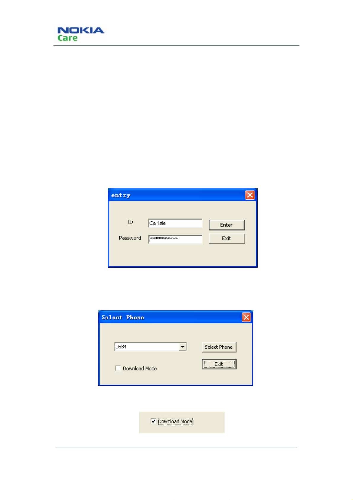
There are three steps to use AMS tool: Firstly, choose Handset and Use mode; secondly, choose the
appropriate function; finally, do related operation with the help of manual.
Select phone and use mode:
Note: When using the download functions, please set the mobile phone in download mode. The
following are steps of entering download mode:
1. Resume power supply after the mobile phone is powered off.
2. Connect your phone with PC, run AMS
3. Input ID and Password and then press the button “Enter” to enter “Select Phone” panel.
ID: Carlisle
Password: 1234@btcsz
After the above actions are completed, you can use the download functions of AMS.
1. Run AMS and pop up “Select Phone” dialogue box:
2. Select “Download Mode” to enter download mode.
COMPANY CONFIDENTIAL
Copyright © 2009 Nokia. All rights reserved.
Issue 1 Page 2-8
Page 31

RH-128
Service Software Instruction
3. Deselect this option if you just want to use general mode.
4. Click “Select Phone” button. The general mode is shown as below.
Download mode is shown as below.
Issue 1 Page 2-9
COMPANY CONFIDENTIAL
Copyright © 2009 Nokia. All rights reserved.
Page 32

RH-128
Service Software Instruction
Select Phone: Activate “Select Phone” in the panel
When the dialogue box is closed, and if you want to use AMS tool, you can re-open the dialogue box in
the panel.
1. In the main menu, select “Phone”.
2. Select the submenu “New” to open a new dialogue box
COMPANY CONFIDENTIAL
Copyright © 2009 Nokia. All rights reserved.
Issue 1 Page 2-10
Page 33

RH-128
Service Software Instruction
Download Mode
Download mode provides only one function, “Emergency Download”.
Emergency Download
Before using “Emergency Download”, you must install some packages in the local PC to support the
software download. This package contains all BIN files requested by mobile phone. The file name is
composed of 5 parts.
For example: RH128_MNV_CL_1500B00_N800
Mode Type
Version info
1900 or 800: RF parameter
Carrier
N: Non-RUIM
R: RUIM
Steps for installing package:
1. Double-click the package you want to install. It displays as below:
2. Click the button “Next >”.
3. Click the button “Install” to start the installation.
Issue 1 Page 2-11
COMPANY CONFIDENTIAL
Copyright © 2009 Nokia. All rights reserved.
Page 34

4. Wait until the installation is finished.
RH-128
Service Software Instruction
5. Click the button “Finish” to exit the installation.
In “Emergency Download”, it is possible to search and display all suitable version files according to the
CPC code input by user. These version files are used for software download.
1. Click the tab to switch to “Emergency Download”
2. It displays as below:
COMPANY CONFIDENTIAL
Copyright © 2009 Nokia. All rights reserved.
Issue 1 Page 2-12
Page 35

RH-128
Service Software Instruction
3. Input CPC code.
4. Click the button “OK”. A list of related version files is displayed.
Issue 1 Page 2-13
COMPANY CONFIDENTIAL
Copyright © 2009 Nokia. All rights reserved.
Page 36

RH-128
Service Software Instruction
NOTE: If the warning dialog pops up, the reason might be one of the following:
1. You have input an incorrect CPC number.
2. You have not installed the appropriate
3. You have not
registered the msxmil4.dll file.
package.
There are four steps to register the msxmil4.dll file.
1. Install MSXML 4.0SP2_cn.msi.
2. Copy msxml4.dll and regist_msxml4_object.bat to the PC path where AMS is installed.
3. Run regist_msxml4_object.bat by double click.
4. If it is registered successfully, restart AMS.
Select the version file you want to download.
COMPANY CONFIDENTIAL
Copyright © 2009 Nokia. All rights reserved.
Issue 1 Page 2-14
Page 37

RH-128
Service Software Instruction
5. The option “Flash Erase” is selected by default. If you don’t need to erase FSM data, you can
deselect this option (it is not recommended to modify the default setup, except for software
developers).
6. Click the button “Download” to start the download.
Issue 1 Page 2-15
COMPANY CONFIDENTIAL
Copyright © 2009 Nokia. All rights reserved.
Page 38

RH-128
Service Software Instruction
7. Wait until the download is finished.
8. Download is finished.
General Mode
The General Mode provides five different functions, including “Phone Information”, “Display Capture”,
“Label Printing”, “Critical Data Backup” and “RF Calibration”. Before using this mode, the handset must
be in Power Up status.
COMPANY CONFIDENTIAL
Copyright © 2009 Nokia. All rights reserved.
Issue 1 Page 2-16
Page 39

RH-128
Service Software Instruction
Phone Information
When getting into General mode, the default is Phone Information which can read out nine parameters
from the handset and display them on the screen.
The nine parameters are Module Number, PSN, ESN, MEID, HWID, Application Code, Language Pack,
Warranty Data and CPC.
1. Switch to “Phone Information”
2. It displays as below:
3. Click button “Refresh” to refresh the current data parameters.
4. Refresh is finished.
Issue 1 Page 2-17
COMPANY CONFIDENTIAL
Copyright © 2009 Nokia. All rights reserved.
Page 40

RH-128
Service Software Instruction
Display Capture
Display Capture is used to capture the screen of the handset and then choose the path to save. The file
can be saved as BMP, JPG and PNG formats.
1. Switch to Display Capture.
2. It displays as below:
COMPANY CONFIDENTIAL
Copyright © 2009 Nokia. All rights reserved.
Issue 1 Page 2-18
Page 41

RH-128
Service Software Instruction
3. Click the button “Begin To Capture” and a box “SnapShot” appears as below:
4. Click the button “Connect”.
5. It displays a connection successful message in dialogue box.
Issue 1 Page 2-19
COMPANY CONFIDENTIAL
Copyright © 2009 Nokia. All rights reserved.
Page 42

6. Click the button “GetImage” to capture the current screen.
7. Click “Option”.
RH-128
Service Software Instruction
8. In “Option”, modify the directory to save the image.
COMPANY CONFIDENTIAL
Copyright © 2009 Nokia. All rights reserved.
Issue 1 Page 2-20
Page 43

RH-128
Service Software Instruction
9. Click “Browse”.
10. Choose the save directory.
11. Click the button “OK” (the left button) to confirm, the save directory is modified and saved.
12. Switch back to “Main”.
Issue 1 Page 2-21
COMPANY CONFIDENTIAL
Copyright © 2009 Nokia. All rights reserved.
Page 44

13. Choose image format.
14. Click the button “SaveImage” to save the image.
RH-128
Service Software Instruction
Notice: When Display Capture is in use, the other AMS functions are disabled.
Label Printing
Label Printing is used to print out the product label. Read out the data from the handset and transfer into
printing file to print it out.
Note: Please make sure you have installed RF Tool Run Time before you using label printing.
Set up the printer before label printing.
Select Start->Control panel->Printer and fax on your PC.
COMPANY CONFIDENTIAL
Issue 1 Page 2-22
Copyright © 2009 Nokia. All rights reserved.
Page 45

RH-128
Service Software Instruction
Click right button to set Zebra 110XiIII Plus (600dpi) printer as the default printer.
Right click the icon, select Properties, choose Port sheet, select Lpt1 port
Click “OK” button, finish the configuration.
It means OK
1. Switch to “Label Printing”.
2. It displays as below:
Issue 1 Page 2-23
COMPANY CONFIDENTIAL
Copyright © 2009 Nokia. All rights reserved.
Page 46

RH-128
Service Software Instruction
3. Click “Refresh”.
4. Read out the data and transfer into printing file.
5. Before printing, you can adjust X, Y offset for proper label print if needed, the default coordinate of
label’s top-left corner is set as (0,0), The latest X, Y offset adjusted by you will be reserved when you
open the tool next time.
COMPANY CONFIDENTIAL
Copyright © 2009 Nokia. All rights reserved.
Issue 1 Page 2-24
Page 47

RH-128
Service Software Instruction
6. Click “print” to start printing.
Critical Data Backup
Critical Data Backup is used to backup the data, i.e. RF parameters.
1. Switch to RF Backup.
2. It displays as below:
3. Click Critical Data Backup to start the backup. The button is disabled.
Issue 1 Page 2-25
COMPANY CONFIDENTIAL
Copyright © 2009 Nokia. All rights reserved.
Page 48

RH-128
Service Software Instruction
4. Five seconds later, the backup is finished. The button is enabled again.
RF Calibration
RF calibration is a tool for automatic tuning of the RF values of target, and automatic testing of the RF
performance.
COMPANY CONFIDENTIAL
Copyright © 2009 Nokia. All rights reserved.
Issue 1 Page 2-26
Page 49

RH-128
Service Software Instruction
1. Click on the RF Calibration tab.
2. RF Calibration screen:
2.1. Log Display Frame
Log Display: calibration information.
2.2. Control Setting Frame
Issue 1 Page 2-27
COMPANY CONFIDENTIAL
Copyright © 2009 Nokia. All rights reserved.
Page 50

RH-128
Service Software Instruction
● Text Window: Show test result.
● Band Select: Switch band.
● Select Action: Calibration or Test.
● Select Function: Enable save Log, Enable Detail UI information and enable Mo call mode.
● Test Set info: Show test set which program auto detected.
3. Program Setting
Config>>Setting
COMPANY CONFIDENTIAL
Copyright © 2009 Nokia. All rights reserved.
Issue 1 Page 2-28
Page 51

RH-128
Service Software Instruction
● GPIB setting: Set GPIB card Number, Callbox Address, and Power Supply Address.
● Phone: Set communicate type.
● Cable Loss: Set cable loss of testing band.
4. Call Config
Config>>Call Config
Configure the parameter when establishing a call, and test.
5. Start Test
Click on the Start button to Setup calibration or test.
Final result will be shown on Text Window.
Click on the Stop button to stop calibration or test on current step.
6. Battery Calibration
In battery Calibration, select Config>>Power supply Control, and set Communicate port as serial
port. Otherwise the battery Calibration value will write default value.
Program support power supply Type:
Agilent E3631, Agilent 66319, Agilent 66309, Agilent 66311, Agilent 66312, Kethley 2306, Kethley
2304, Kethley 2303, Kethley 2302.
Issue 1 Page 2-29
COMPANY CONFIDENTIAL
Copyright © 2009 Nokia. All rights reserved.
Page 52

Service Software Instruction
7. RF Calibration & Performance test
Program support Callbox Type:
Agilent 8960, R&S CMU200.
8. Error Code
Use Error Translate tool to help explain the cause of a failed test.
Enter the Error code in Error Code String window, click on OK button. The detailed error
information will show Text window. For example, Error code: 17815, can Translate as shown
below:
RH-128
DebugTool
DebugTool overview
The DebugTool is used for online debugging and repair analysis.
COMPANY CONFIDENTIAL
Copyright © 2009 Nokia. All rights reserved.
Issue 1 Page 2-30
Page 53

RH-128
Service Software Instruction
There are several function areas in the main screen. There are 3 buttons, including an error code
translate tool button, a configure setting button and a quit program button. A text message box shows
the command sent out and received.
Config and Error code Translate
Config
Config setting panel can set com port type (USB or Serial), com port number, and baud rate.
Error code Translate
Enter the error code in Error Code text box, then click on OK button. Error code will be Translated in the
message window.
Issue 1 Page 2-31
COMPANY CONFIDENTIAL
Copyright © 2009 Nokia. All rights reserved.
Page 54

RH-128
Service Software Instruction
Log
Debugtool creates a log file after the Via hub Setup. All operations on the main panel will be recorded in
this log. The log is stored in the folder in local dir of program.
A sample log is shown as below. This file is named by create time.
Text Info
All operations are displayed in this window.
COMPANY CONFIDENTIAL
Copyright © 2009 Nokia. All rights reserved.
Issue 1 Page 2-32
Page 55

RH-128
Service Software Instruction
Setup communication
Setup Hub for communication. All the buttons are dimmed when the program is open. To activate the
buttons and setup soft hub, first click on the Setup Hub button.
Then wait for all buttons to be activated.
Issue 1 Page 2-33
COMPANY CONFIDENTIAL
Copyright © 2009 Nokia. All rights reserved.
Page 56

RH-128
Service Software Instruction
Release hub will disconnect the communication. Then all the buttons are deactivated.
Enter calibration mode
All BB and RF calibration must be done in calibration mode. This mode can be entered when the phone
is switched on and in boot waiting time (only 1.5s). This mode can also be entered when the power is
already on.
In this chapter, use the Initial frame.
Enter when phone on.
A. Start with power supply power down.
B. Click on the Boot To Loader button.
C. Power on. Wait for phone to stop on boot.
D. Click on the Enter Cal Mode button.
E. Click on the Jump Loader button. Then wait for 3s to 5s, the phone is in the calibration mode.
Enter after phone on.
A. Start with power supply power on until the phone is fully on.
B. Click on the Jump Loader button.
D. Click on the Enter Cal Mode button.
E. Click on the Jump Loader button. Then wait for 3s to 5s, the phone is in the calibration mode.
COMPANY CONFIDENTIAL
Copyright © 2009 Nokia. All rights reserved.
Issue 1 Page 2-34
Page 57

RH-128
Service Software Instruction
PSN SFC read and writing
PSN is the product serial number. SFC is the keyword for MES.
In this chapter, use the Process frame.
CDMA Battery Measurement Calibration
Calibration method
Select some groups of voltage value, switch them to corresponding Aux ADC values and write them into
memory. Calibration steps: Select 5 groups of voltage value, switch them to 5 groups of Aux ADC
numerical value via AD.
Calibration Procedure
A. Start with reset system (PS power down, reset).
B. Set the power supply to the desired value.
C. Get the Aux ADC Value from the Debug Tool. The battery AUX ADC detect channel is 1, the on/off
status is on. Click on the Get Result button to get ADC value.
D. Try more than 5 times. Get the average value. Store the power supply voltage point versus the Aux
ADC value.
E. Iterate steps B - D once for another power supply voltage.
Issue 1 Page 2-35
COMPANY CONFIDENTIAL
Copyright © 2009 Nokia. All rights reserved.
Page 58

RH-128
Service Software Instruction
CDMA RxAGC Calibration
Supported receiver calibration items are the following:
CP DB HWD PCS RxAGC
CP DB HWD PCS RxAGC Freq Chan Adj
Note: Before starting the RxAGC Calibration, the Rx date must be set empty. Otherwise the calibration
value may not be correct.
CDMA RxAGC Baseline
CDMA RxAGC Baseline overview
The basic mechanism for calibration is to provide a signal of known power at the antenna, allow the
RxAGC to settle, and make note of the resulting RxAGC PDM value. In this way, the “settled” value of
the PDM for a given Rx power is known.
Calibration Procedure
A. Start with reset system (PS power down, reset).
B. Click on CP Enable/Disable and CP Power Down/Up. Let the CP disable and power down.
C. Set the channel. Set the control mode to Manual, and the band to the target band.
D. Set the test set frequency channel to the test frequency. For the first data point, enter the channel
used to calibrate the Rx AGC. Then set the test set transmission power to a desired power which is in
the Rx highest gain. The Reference Level is -99dB.
E. Initialize the calibration RxAGC gain state by clicking on DSPM Rfc Dagc. Set gain state to highest
gain.
F. Click on DSPM Spy Enable/Disable.
COMPANY CONFIDENTIAL
Copyright © 2009 Nokia. All rights reserved.
Issue 1 Page 2-36
Page 59

RH-128
Service Software Instruction
The Spy windows become active, and display the current Tx and Rx status.
G. Get the RxDAgc Value Bitsel and the RxDAgc Value Gain. Write those calibration parameters
together with Reference Level to the non-volatile area of flash memory. To confirm the new calibration,
first update the Flash by either power cycling the UUT or by using the CalMode Select with the NVRAM
option.
H. Calibrate the Gain offset. Set the test set transmission power to the desired power which is
between the switch point of each gain level. Calibrate the gain level from the high gain to low gain. Set
the calibration RxAGC gain state by clicking on DSPM Rfc Dagc.
I. Get the received power form the Spy window. For example, if the BS power is -85dBm, and the gain
state is 3, we get -96dBm from spy window. The offset of gain 4 to gain 3 is -85 – (-96) = 11dBm. Write
the calibration parameters to the non-volatile area of flash memory. Confirm the new calibration result.
J. Iterate steps H - I for all desired calibration points.
CDMA RxAGC Frequency Channel Adjustment
About CDMA RxAGC Frequency Channel Adjustment
This procedure is performed at only one power setting. This procedure assumes that the baseline
RxAGC calibration table has been loaded into NVRAM. However, if the calibration application (running
on a PC) stores the RxAGC tables from Section 7.2.1 in PC memory, then the PC Application can
interpolate dBm power values from the PDM value returned by Debugtool. More details are provided
below in the steps below.
CDMA RxAGC Frequency Channel Adjustment Procedure
Issue 1 Page 2-37
COMPANY CONFIDENTIAL
Copyright © 2009 Nokia. All rights reserved.
Page 60

RH-128
Service Software Instruction
A. Perform the procedure at “nominal” or room temperature.
B. The baseline RxAGC calibration must have already been completed.
C. The RxAGC frequency channel adjustment, and temperature adjustment tables must be zeroed.
D. Connect the antenna to CDMA test set.
E. Reset the UUT, start Debugtool, and do not press the Power key on the Virt MMI (i.e., PS should
be off and LID reset). Send the message CP Enable, with Disable option.
F. Set the test set Transmission Power to a desired power point (-100 dBm is a suggested value). This
is normally a point that is calibrated during Rx AGC calibration.
G. Set the test set frequency channel to the test frequency. For the first data point, enter the channel
used to calibrate the RX AGC.
H. Set the frequency channel to the calibration frequency using the CP PLL Channel Config. For the
first data point, enter the channel used to calibrate the RX AGC. Set the Control mode as Manual, the
band to target band.
I. Allow for 25 ms (or more) of settle time.
J. Get the RxAGC Antenna Power (dBm) value using the DSPM Rx AGC Get Parms. As show in the
picture, we get received power -101.1dBm.
K. Calculate Error Power = Transmission Power – Antenna Power, where the Transmission Power
was set in step F and the Antenna Power was obtained in step J. Store the Error Power (dB) versus the
frequency channel point in the non-volatile area of flash memory.
L. Iterate steps G - K for all desired calibration points.
CDMA TxAGC Calibration
There are multiple tables for calibration of the transmitter. All curves must be generated for all band
classes and for all Tx hysteresis states that are utilized.
Supported Transmitter calibration items are the following:
● CP DB HWD PCS TxAGC
COMPANY CONFIDENTIAL
Copyright © 2009 Nokia. All rights reserved.
Issue 1 Page 2-38
Page 61

RH-128
Service Software Instruction
● CP DB HWD PCS TxAGC Freq Chan Adj
● CP DB HWD PCS Tx Limit Freq Chan Adj
● CP DB HWD PCS Tx Power Detect
● CP DB HWD PCS Tx Power Detect Freq Chan Adj
CDMA TxAGC Baseline
CDMA TxAGC Baseline overview
The basic mechanism of the calibration is to transmit a signal at the antenna port with a certain PDM
setting, the power of which is measured by a power meter, spectrum analyzer, or CDMA test set. The
PDM setting and resulting power are then recorded. Care should be taken to provide enough calibration
points near maximum power to ensure accurate transmission power at this level.
CDMA TxAGC Baseline Procedure
A. Perform the procedure at “nominal” or room temperature.
B. The baseline RxAGC calibration must have already been completed.
C. The RxAGC frequency channel adjustment, and temperature adjustment tables must be zeroed.
D. Connect the antenna to CDMA test set.
E. Reset the UUT, start Debugtool, and do not press the Power key on the Virt MMI (i.e., PS should
be off and LID reset). Send the message CP Enable, with Disable option.
F. Set the frequency channel to the calibration frequency using the PLL Channel Config. This is the
baseline frequency, since the frequency compensation table is not active. Set the Control mode as
Manual, the band to target band.
G. Initialize the TxAGC PDM (HW Val in the box below) with a suitably low known value, to prevent a
potential surge of Tx power when the transmitter is turned on in the next step. Use the DSPM Tx AGC
Config. Set the Mode as Manual, the Method as HW_Value, the Hyst as current state.
Issue 1 Page 2-39
COMPANY CONFIDENTIAL
Copyright © 2009 Nokia. All rights reserved.
Page 62

RH-128
Service Software Instruction
H. Turn on the transmitter using the Tx Rate. Set the Rate is Tr Full Rate.
I. Set up the spectrum analyzer or test set to measure the channel power on the same channel
selected in step F.
J. Vary the HW Val until the reported power is within +/-1 dB of the desired power level using DSPM
Tx AGC Config.
K. Store the reported test set channel power (dBm) versus PDM value point in the non-volatile area of
flash memory.
L. Iterate steps G to K for all desired calibration points and Write to store the values.
M. Repeat steps G – L for all desired gain points.
CDMA TxAGC Frequency Channel Adjustment
CDMA TxAGC Frequency Channel Adjustment overview
To perform this calibration, the baseline Tx AGC calibration should have already been performed. This is
performed for all gain states.
CDMA TxAGC Frequency Channel Adjustment Procedure
A. Perform the procedure at “nominal” or room temperature.
B. The baseline RxAGC calibration must have already been completed.
C. The RxAGC frequency channel adjustment, and temperature adjustment tables must be zeroed.
D. Connect the antenna to CDMA test set.
E. Reset the UUT, start Debugtool, and do not press the Power key on the Virt MMI (i.e., PS should
be off and LID reset). Send the message CP Enable, with Disable option.
F. Turn off the transmitter test using the Tx Rate Test with the rate set to Tr Full Rate.
G. Set the frequency channel to the channel used for calibrating the TX AGC using the PLL Channel
Config. CP PLL Channel Config Settings, Ctrl Mode: Manual, Band: Band being calibrated, Channel:
Channel being calibrated.
COMPANY CONFIDENTIAL
Copyright © 2009 Nokia. All rights reserved.
Issue 1 Page 2-40
Page 63

RH-128
Service Software Instruction
H. Set the measurement equipment to the frequency channel used for calibrating the TX AGC (see
step F).
I. Turn on the transmitter test using the Tx Rate Test with the rate set to Tr Full Rate.
J. Set the Tx power by direct control of the dBm setting using TxAGC Config. DSPM Tx AGC Config
Settings, Ctrl Mode: Manual, Method: dB Gain, HW Val: N/A, Hyst State: N/A, Power (dBm): Middle of
band being calibrated (This is the Target Tx Power).
K. Get the Measured Tx Power from the CDMA test set or other measuring device and calculate:
Antenna Power Error = Target Tx Power - Measured Tx Power
L. Store the Antenna Power Error (dB) versus frequency channel point in the non-volatile area of flash
memory.
M. Iterate steps F to L for all desired calibration points and Write to store the values.
N. Repeat steps F – M for all desired gain points.
CDMA TxAGC Max Power Limit Frequency Adjustment
CDMA TxAGC Max Power Limit Frequency Adjustment overview
In order to perform this calibration, the other Tx AGC calibrations should have already been performed.
This procedure is performed for only one gain state, the highest gain stage, since this table only applies
to max power.
CDMA TxAGC Max Power Limit Frequency Adjustment procedure
A. Baseline TxAGC calibration tables must be loaded.
B. The Tx Limit Freq Chan Adj table must be cleared (write zeros in the DBM template).
C. This procedure is identical to the procedure described in above section, but must be performed at
the Max Power Level.
D. Write calibration parameters to the non-volatile area of flash memory.
Issue 1 Page 2-41
COMPANY CONFIDENTIAL
Copyright © 2009 Nokia. All rights reserved.
Page 64

RH-128
Service Software Instruction
CDMA TxAGC Closed Loop RF Power
CDMA TxAGC Closed Loop RF Power overview
The procedure for baseline, temperature adjustment and frequency channel adjustment is the same as
that for calibration of the dBm to PDM value tables as described in above Sections, except that the Tx
power detection ADC should be read using Aux ADC Get.
CDMA TxAGC Closed Loop RF Power Procedure.
A. Perform the procedure at “nominal” or room temperature.
B. The baseline RxAGC calibration must have already been completed.
C. The RxAGC frequency channel adjustment, and temperature adjustment tables must be zeroed.
D. Connect the antenna to CDMA test set.
E. Reset the UUT, start Debugtool, and do not press the Power key on the Virt MMI (i.e., PS should
be off and LID reset). Send the message CP Enable, with Disable option.
F. Set the measurement equipment to the frequency channel used for calibrating the TX AGC
G. Turn off the transmitter test using the Tx Rate Test with the rate set to Tr Full Rate.
H. Set the frequency channel to the channel used for calibrating the TX AGC using the PLL Channel
Config. CP PLL Channel Config Settings, Ctrl Mode: Manual ,Band: Band being calibrated , Channel:
Channel being calibrated. (see step F).
I. Turn on the transmitter test using the Tx Rate with the rate set to Tr Full Rate.
J. Set the Tx power by direct control of the dBm setting using DSPM TxAGC Config. Vary the HW Val
until the reported power is within +/-1 dB of the desired power level using DSPM Tx AGC Config. DSPM
Tx AGC Config Settings, Ctrl Mode: Manual, Method: dB Gain ,HW Val: N/A, Hyst State: N/A, Power
(dBm): Some starting value
COMPANY CONFIDENTIAL
Copyright © 2009 Nokia. All rights reserved.
Issue 1 Page 2-42
Page 65

RH-128
Service Software Instruction
K. Send the Aux ADC Get, a number of times (10 is good) and take the average. CP AUX ADC Get
Settings, AUX ADC Channel: Design specific, Tx PCG Sync: On.
L. Iterate steps J to K for all desired calibration points and Write to store the values.
CDMA TxAGC Closed Loop Frequency Channel Adjustment
CDMA TxAGC Closed Loop Frequency Channel Adjustment overview
In order to perform this calibration, the baseline Tx AGC calibration should have already been
performed. This is performed for only one gain state.
CDMA TxAGC Closed Loop Frequency Channel Adjustment Procedure
A. Perform the procedure at “nominal” or room temperature.
B. The baseline RxAGC calibration must have already been completed.
C. The RxAGC frequency channel adjustment, and temperature adjustment tables must be zeroed.
D. Connect the antenna to CDMA test set.
E. Reset the UUT, start Debugtool, and do not press the Power key on the Virt MMI (i.e., PS should
be off and LID reset). Send the message CP Enable, with Disable option.
F. Turn off the transmitter test using the Tx Rate Test with the rate set to Tr Full Rate.
G. Set the frequency channel to the calibration frequency using PLL Channel Config. This is the
baseline frequency, since the frequency compensation table is not active.
H. Set the frequency channel to the channel used for calibrating the TX AGC using the PLL Channel
Config. CP PLL Channel Config Settings, Ctrl Mode: Manual ,Band: Band being calibrated , Channel:
Channel being calibrated.
Issue 1 Page 2-43
COMPANY CONFIDENTIAL
Copyright © 2009 Nokia. All rights reserved.
Page 66

RH-128
Service Software Instruction
I. Turn on the transmitter test using the Tx Rate with the rate set to Tr Full Rate.
J. Set the Target Tx Power by direct control of the dBm setting using DSPM TxAGC Config. Vary the
HW Val until the reported power is within +/-1 dB of the desired power level using DSPM Tx AGC Config.
DSPM Tx AGC Config Settings, Ctrl Mode: Manual, Method: dB Gain ,HW Val: N/A, Hyst State: N/A,
Power (dBm): Some starting value
K. Set the measurement equipment to the measurement frequency channel.
L. Get the Measured Tx Power (over the 1.25 MHz bandwidth) from the CDMA test set (or other
measuring device) and get the Closed Loop Tx Power from the Current Tx Power.
The true power calculate: Read Power / 64 = True Power (dB)
M. Calculate Power Error = Measured Tx Power - Closed Loop Tx Power .
N. Store the Power Error (dB) versus frequency channel point.
O. Iterate steps 7, 10-12 for all desired calibration points.
P. Write calibration parameters to the non-volatile area of flash memory
COMPANY CONFIDENTIAL
Copyright © 2009 Nokia. All rights reserved.
Issue 1 Page 2-44
Page 67

RH-128
Service Software Instruction
Error Code
Three class error code
Use Error Translate tool to help explain the cause of a failed test.
Enter the Error code in Error Code Stringwindow, click on OK button. The detail error information will
show in the Textwindow shown below. For example, Error code: 17815, can Translate as shown.
Error Message Table
[Error_Class_3]
1000 INIT_SetUp_ETSCOMPort_ERROR
3000 INIT_ModeSetting_ERROR
2000 Check_CPSWHWVersion_Compare_ERROR
4000 Check_CheckProcessBit_ERROR
Process control Error
5000 Check_BandSelect_ERROR
6000 Check_EndProcess_ERROR
7000 Cal_InitValue_ERROR
23000 Process_CheckBit_ERROR
8000 Cal_TxAGCBaseCal_ERROR Calibration Error
Issue 1 Page 2-45
COMPANY CONFIDENTIAL
Copyright © 2009 Nokia. All rights reserved.
Page 68

9000 Cal_RxAGCBaseCal_ERROR
10000 Cal_TxAGCFREQCHAN_ERROR
11000 Cal_RxAGCFREQCHAN_ERROR
12000 Cal_TxAGCLIMFREQCHAN_ERROR
13000 Cal_TxAGCCLOSEDRFPWR_ERROR
14000 Cal_TxAGCCLOSEDFREQCHAN_ERROR
15000 Cal_WriteTemperatureDB_ERROR
16000 Cal_WriteBatteryDB_ERROR
17000 Cal_HWDBatteryCal_ERROR
18000 PTest_SetupCall_ERROR
19000 PTest_CallInitial_ERROR
20000 PTest_CallBandInitial_ERROR
21000 PTest_CallConnectFunction_ERROR
22000 PTest_QuickPerformanceTest_ERROR
39000 Loopback_Call_ERROR
[Error_Class_2]
390 INSTR_INSTRUMENTNULL_ERROR
400 INSTR_SETUP8960_ERROR
410 INSTR_SETCABLELOSS_ERROR
420 INSTR_WRITESECAPWR_ERROR
430 INSTR_SETONOFFSECAPER_ERROR
440 INSTR_WRITERFCHANNEL_ERROR
450 INSTR_SETUPTESTSET_ERROR
460 INSTR_RFPORTSET_ERROR
470 INSTR_SETIM2_ERROR
480 INSTR_SETOPERATINGMODE_ERROR
490 INSTR_SETITC_ERROR
500 INSTR_GETCURRPER_ERROR
510 INSTR_SETTXDYNAMIC_ERROR
520 INSTR_SETTXDYNAMICINIT_ERROR
530 INSTR_RESTORETXDYNAMIC_ERROR
540 INSTR_MEASTXDYNAMIC_ERROR
550 INSTR_RESETTESTSET_ERROR
560 INSTR_QUERYFSTATUS_ERROR
570 INSTR_PRINTFFATATUS_ERROR
580 INSTR_SETMEASSPEED_ERROR
590 INSTR_SWITCHPOWER_ERROR
600 INSTR_SETVOLTAGECURRENT_ERROR
610 INSTR_READCURRENT_ERROR
620 INSTR_SINGLECHIPCOMMUNICATE_ERROR
810 INSTR_Callbox_Initial_ERROR
RH-128
Service Software Instruction
Performance Test Error
Instrument Communicate
Error
COMPANY CONFIDENTIAL
Copyright © 2009 Nokia. All rights reserved.
Issue 1 Page 2-46
Page 69

RH-128
Service Software Instruction
820 INSTR_PowerSupply_Initial_ERROR
830 INSTR_GPIBCard_ERROR
20 ETSCommand_Get_BootToLoader_ERROR
30 ETSCommand_EnterCalbrationMode_ERROR
40 ETSCommand_JumoToLoader_ERROR
50 ETSCommand_Loopback_ERROR
60 ETSCommand_CPOff_ERROR
70 ETSCommand_PowerDown_ERROR
80 ETSCommand_SNReadWrite_ERROR
90 ETSCommand_ProcessBit_RW_ERROR
100 ETSCommand_TestSWVersion_RW_ERROR
110 ETSCommand_CPSWHWVersionRead_ERROR
120 ETSCommand_DBFlush_ERROR
130 ETSCommand_RFBackup_ERROR
140 ETSCommand_DBClear_ERROR
150 ETSCommand_InitialNVRAM_ERROR
160 ETSCommand_AFCData_WriteDB_ERROR
170 ETSCommand_BandGapData_WriteDB_ERROR
180 ETSCommand_Battery_AUXValGet_ERROR
190 ETSCommand_Battery_WriteDB_ERROR
200 ETSCommand_TransmitOnOff_ERROR
210 ETSCommand_SetPLLConfig_ERROR
220 ETSCommand_TxRateSet_ERROR
230 ETSCommand_DSPMTxAGCConfig_ERROR
240 ETSCommand_RF_WriteDB_ERROR
250 ETSCommand_HWResultDetect_OverRange_ERROR
260 ETSCommand_ModesEnableSlotted_ERROR
270 ETSCommand_ReceiverOnOff_ERROR
280 ETSCommand_DSPMRfcDagcSetGain_ERROR
290 ETSCommand_DSPMSpyEnable_ERROR
300 ETSCommand_DSPMSpyGet_ERROR
310 ETSCommand_DSPMSpyGet_Empty_ERROR
320 ETSCommand_BitselGain_Detect_ERROR
330 ETSCommand_DSPMRxAgcGet_ERROR
340 ETSCommand_PowerDetect_AUXValGet_ERROR
350 ETSCommand_ReadCurrentTxPower_ERROR
360 ETSCommand_CallInitiate_ERROR
670 RFPT_OffCurrent_ERROR
680 RFPT_PowerOnCurrent_ERROR
690 RFPT_CallCurrent_ERROR
700 RFPT_RxSensitivity_ERROR
Phone Communicate
Command Error
Performance Test Error
Issue 1 Page 2-47
COMPANY CONFIDENTIAL
Copyright © 2009 Nokia. All rights reserved.
Page 70

Service Software Instruction
710 RFPT_MaxPower_ERROR
720 RFPT_TxSpuriousTest_ERROR
730 RFPT_MinPower_ERROR
740 RFPT_WaveformCodeDomain_ERROR
750 RFPT_TimeRspVsOpenloop_ERROR
760 RFPT_GetedPower_ERROR
780 XMLMsg_Response_Null_ERROR
790 XMLMsg_Response_Corresponding_ERROR
MES Communicate Error
800 XMLMsg_Response_Java_ERROR
840 XML_SFC_ReadWrite_ERROR
980 Result_OverRange_ERROR Test Result Error
990 Error_Max_Other
[Error_Class_1]
8 Result_OverRange_Low_ERROR
Test Result Error
9 Result_OverRange_High_ERROR
2 CMD_SETTING_ERROR
3 CMD_COMMANDSEND_ERROR
4 CMD_FINDRESPONSE_ERROR
Phone Communicate Error
5 CMD_RSPCORRESPOND_ERROR
6 CMD_VIACMD_ERROR
7 CMD_RESPONSENULL_ERROR
RH-128
COMPANY CONFIDENTIAL
Issue 1 Page 2-48
Copyright © 2009 Nokia. All rights reserved.
Page 71

Nokia Customer Care
3- Service Tools
COMPANY CONFIDENTIAL
Copyright © 2009 Nokia. All rights reserved.
Page 3-1 Issue 1
Page 72

RH-128
Service Tools
(This page left intentionally blank.)
COMPANY CONFIDENTIAL
Copyright © 2009 Nokia. All rights reserved.
Issue 1 Page 3-2
Page 73

RH-128
Service Tools
Table of Contents
Introduction......................................................................................................................................... page3-5
Service configuration......................................................................................................................... page3-5
Service tools............................................................................................................................... page3-5
Service configuration.................................................................................................................page3-6
MJ-200 handling instructions............................................................................................................ page3-6
External connections & switch instructions............................................................................page3-6
MJ-200 PWB pin definition........................................................................................................page3-8
Handling instruction.................................................................................................................. page3-8
Power on sequence.......................................................................................................................... page3-10
Issue 1
COMPANY CONFIDENTIAL
Copyright © 2009 Nokia. All rights reserved.
Page 3-3
Page 74

RH-128
Service Tools
(This page left intentionally blank.)
COMPANY CONFIDENTIAL
Copyright © 2009 Nokia. All rights reserved.
Issue 1 Page 3-4
Page 75

RH-128
Service Tools
Introduction
This document explains relevant service software, service tools and handling instructions for RH-128.
Service configuration
Service tools
The table below gives an overview of service tools with Module jig that would be used in service testing,
tuning and error analysis.
CA-101 Data Service Cable
This cable provides a connection from the USB port of the personal
computer or notebook to the micro USB connector of the phone and
allows Point of Sale (POS) locations to flash the mobile terminal.
MJ-200 Module Jig
This jig allows PWB-level service and troubleshooting. It supports
regulated and unregulated DC input voltages, a headset jack for audio
tests and a RUIM card reader. It also supports simultaneous RF
connections to the CDMA engine.
AK05G-0650400W2 AC power adapter
This AC power adapter (with 5.50mm power cord connector) is used to
provide DC power to the mobile phone and service tools (e.g. Module
Jig) from power supply for CDMA tuning (packaged with the module jig).
CA-128RS RF Service Cable
This test cable is used for RF engine testing and tuning. It snaps directly
on the mobile terminal’s RF connector and converts the output to a
Issue 1
surface mounting assembly connector.
COMPANY CONFIDENTIAL
Copyright © 2009 Nokia. All rights reserved.
Page 3-5
Page 76

PK-86 AMS SW Protection Key
This hardware dongle connected to the USB port of the service
computer, enables the use of the service software. It is not possible to
use the service software without the dongle.
Service configuration
The following diagram illustrates service setup with Module Jig.
RH-128
Service Tools
MJ-200 handling instructions
External connections & switch instructions
COMPANY CONFIDENTIAL
Copyright © 2009 Nokia. All rights reserved.
Issue 1 Page 3-6
Page 77

RH-128
Service Tools
1- Micro USB connector
2- S101 Power Key (turn power “on” when starting )
3- U52 banana connectors for current meter (0~1A)
4- S1 switch for current measurement
5- U51 banana connectors for back up power supply DC 3.7V~4.2V
6- Serial Port (connect 9 pin serial cable with PC for battery calibration and RF calibration )
7- CN101 AC Power Supply connector (for AC adapter or power service cable 6.5V~7.5V. 1A)
8- S102 for main power and back up power switch
9- S2 Download/Test mode switch (Turn “off” when using the module jig, enter download mode by
pressing and holding up key on keypad)
10- UIM slot
Issue 1
COMPANY CONFIDENTIAL
Copyright © 2009 Nokia. All rights reserved.
Page 3-7
Page 78

MJ-200 PWB pin definition
RH-128
Service Tools
Handling instruction
1. Put PWB onto the module jig.
COMPANY CONFIDENTIAL
Copyright © 2009 Nokia. All rights reserved.
Issue 1 Page 3-8
Page 79

RH-128
Service Tools
2. Close the module jig up.
Issue 1
COMPANY CONFIDENTIAL
Copyright © 2009 Nokia. All rights reserved.
Page 3-9
Page 80

3. Connection with PC
RH-128
Service Tools
1) RF calibration
RF Cable provides a connection from RF connector on the jig to RF connector on CMU200 or
Agilent8960 and executes RF calibration function in AMS.
2) SW update / flashing
USB Cable CA-101 provides a connection from the USB port of the personal computer or notebook to
the micro USB connector on Module jig for SW update/flashing.
3) Full Phone functionality
Press #0000# , select CIT test >Manual test to perform the phone functionality check.
Power on sequence
1. S
@ VCC1 (Power Supply 1 :AC adapter or power service cable
102
:6.5V-7.5V,I
V
cc1
max
=1A); S
@ VCC2(Power Supply 2)
102
2. S1@ on(power on )
3. S
@ On(main current ); S
101
@ Off (adding a current meter between two red banana
101
connectors U52 for current measurement)
4. S2 @off (test mode)
COMPANY CONFIDENTIAL
Copyright © 2009 Nokia. All rights reserved.
Issue 1 Page 3-10
Page 81

Nokia Customer Care
4- Antenna Description
COMPANY CONFIDENTIAL
Copyright © 2009 Nokia. All rights reserved.
Page 4-1 Issue 1
Page 82

RH-128
Antenna Description and Troubleshooting
(This page left intentionally blank.)
Page 4-2 Issue 1
COMPANY CONFIDENTIAL
Copyright © 2009 Nokia. All rights reserved.
Page 83

RH-128
Antenna Description and Troubleshooting
Table of Contents
Introduction...................................................................................................................................................... page 4-5
Visual quality requirements................................................................................................................... page 4-5
Failures and corrective measures.................................................................................................................. page 4-5
Damaged RF feed point pin....................................................................................................................page 4-6
Obstructed RF feed point pad........................................................................................................................ page 4-7
RF connector failure........................................................................................................................................ page 4-8
Issue 1
COMPANY CONFIDENTIAL
Page 4-3
Copyright © 2009 Nokia. All rights reserved.
Page 84

RH-128
Antenna Description and Troubleshooting
(This page left intentionally blank.)
Page 4-4 Issue 1
COMPANY CONFIDENTIAL
Copyright © 2009 Nokia. All rights reserved.
Page 85

RH-128
Antenna Description and Troubleshooting
Introduction
The mobile terminal includes an internal antenna. This antenna arrangement is used for Cellular frequency
bands. The internal antenna assembly adopts Monopole Antenna structure used for the cellular engine.
Visual quality requirements
Below are the minimum acceptable visual quality requirements of the internal antenna assembly:
z Wear gloves to assemble the antenna. Don’t touch the antenna radiator with bare hands.
z No visual cracks or mechanical defects.
z No oil, dirt or particles attached on the parts.
z Radiator must be flat without warping and aligned with the plastic housing.
z The length of all pins must be identical and the pins align.
Failures and corrective measures
The two antennas are assembled into B Cover as shown in Figure 1. If no internal antenna is installed, the
antenna gain is degraded by more than 20 dB.
z If the internal antenna is missing, install antenna-asm Module.
z If the radiator is damaged, replace it with a new antenna-asm Module.
Figure 1: B Cover Assembly
Issue 1
Page 4-5
COMPANY CONFIDENTIAL
Copyright © 2009 Nokia. All rights reserved.
Page 86

RH-128
Antenna Description and Troubleshooting
Damaged RF feed point pin
The pin (spring clip) of the antenna must be properly connected to the PWB.
z If the main antenna’s RF feed point pin does not touch the PWB, the antenna gain degrades by more
than 17 dB.
z If the RF feed pin is broken or bent, replace the antenna-asm Module.
z If the RF feed pin spring turns out damaged, replace the antenna-asm Module.
Figure 2: Back view of internal antennas
Page 4-6 Issue 1
COMPANY CONFIDENTIAL
Copyright © 2009 Nokia. All rights reserved.
Page 87

RH-128
Antenna Description and Troubleshooting
Obstructed RF feed point pad
If the RF feed point pad is obstructed, removed or covered, the antenna pin does not touch the PWB and
the antenna performance degrades.
z If there is any corrosion or the pad is missing, replace the PWB.
z If a pad is obstructed or covered by something, clean the pad.
z If any component of antenna match circuit is missing, replace the related component.
Figure 3: PWB layout of RF feed point and antenna match circuit
Issue 1
Page 4-7
COMPANY CONFIDENTIAL
Copyright © 2009 Nokia. All rights reserved.
Page 88

RH-128
Antenna Description and Troubleshooting
RF connector failure
The RF connector fails when it does not properly connect RF input terminal to RF output terminal during
SMT. If this happens the antenna gain degrades by 25 dB. Check this failure by measuring the resistance
value between the input and output of RF connector, if the value is close to zero, replace the RF connector.
Note:
Do not insert RF cable to RF connector when testing the resistance value. Because the RF connector
is also a switch, when RF cable is inserted, RF output is disconnected from RF input.
z RF input terminal – connect to duplexer.
z RF output terminal – connect to the antenna pad through antenna match circuit.
z RF connector terminal – connect to RF coaxial cable.
Figure 4: RF input / output terminal
Page 4-8 Issue 1
COMPANY CONFIDENTIAL
Copyright © 2009 Nokia. All rights reserved.
Page 89

Nokia Customer Care
5- Baseband Description and
Troubleshooting
COMPANY CONFIDENTIAL
Copyright © 2009 Nokia. All rights reserved.
Page 5-1 Issue 1
Page 90

RH-128
Baseband Description and Troubleshooting
(This page left intentionally blank.)
COMPANY CONFIDENTIAL
Copyright © 2009 Nokia. All rights reserved.
Issue 1 Page 5-2
Page 91

RH-128
Baseband Description and Troubleshooting
Table of Contents
Key components overview................................................................................................................ page 5-5
System block diagram.......................................................................................................................page 5-6
Platform Introduction.........................................................................................................................page 5-6
CBP 5.0....................................................................................................................................... page 5-6
Power Up.................................................................................................................................... page 5-9
Power Off................................................................................................................................... page 5-9
Clock Distribution..................................................................................................................... page 5-9
Power Distribution.................................................................................................................. page 5-10
VC-TCXO.................................................................................................................................. page 5-11
Battery...................................................................................................................................... page 5-11
Display and Keypad.........................................................................................................................page 5-12
Troubleshooting............................................................................................................................... page 5-13
Power Does Not Stay ON.................................................................................................................page 5-13
Power Does Not Stay ON Troubleshooting...........................................................................page 5-14
Audio Faults..................................................................................................................................... page 5-15
No Sound in Earpiece & Microphone (refer to Audio PA Circuit design)...........................page 5-15
Audio Faults Troubleshooting............................................................................................... page 5-16
Audio PA Circuitry...................................................................................................................page 5-18
Display Faults................................................................................................................................... page 5-18
Display Faults Troubleshooting............................................................................................. page 5-18
Keypad Faults ..................................................................................................................................page 5-20
Keypad Faults Troubleshooting.............................................................................................page 5-20
Vibrator Faults (reference to the Vibrator Circuit Design)........................................................... page 5-21
No Vibration T roubleshooting................................................................................................ page 5-21
Vibrator Circuit........................................................................................................................ page 5-22
USB Interface Faults........................................................................................................................page 5-23
USB Interface Disabled Troubleshooting..............................................................................page 5-23
USB Circuitry...........................................................................................................................page 5-24
UIM Card Unreadable troubleshooting.......................................................................................... page 5-24
Charging Faults Troubleshooting...................................................................................................page 5-25
Issue 1
COMPANY CONFIDENTIAL
Copyright © 2009 Nokia. All rights reserved.
Page 5-3
Page 92

RH-128
Baseband Description and Troubleshooting
(This page left intentionally blank.)
COMPANY CONFIDENTIAL
Copyright © 2009 Nokia. All rights reserved.
Issue 1 Page 5-4
Page 93

RH-128
Baseband Description and Troubleshooting
Key components overview
Component Model Number Supplier
Baseband processor CBP 5.0 VIA
PMU ACT5805 Active
Memory TV00560002EDGB TOSHIBA
LCD BM4531J BYD
Issue 1
Figure 1 Component layout
COMPANY CONFIDENTIAL
Copyright © 2009 Nokia. All rights reserved.
Page 5-5
Page 94

System block diagram
RH-128
Baseband Description and Troubleshooting
Platform Introduction
CBP 5.0
VIA Telecom’s CBP 5.0 single-chip CDMA Base Band Processors provide a complete 3G CDMA2000®
1X (Release 0) solution. They are designed to meet or exceed the specifications of mobile stations for
worldwide 3G CDMA systems as specified by CDMA2000® 1X (Release 0) standards and are
backward-compatible to IS -95.
CBP 5.0 integrates three processor subsystems
ARM7TDMI® Control Processor (CP) supports the protocol stack, user interface, and hardware
interface processing. Two TeakLite® Digital Signal Processors (DSPs): one DSP supports CDMA
modem processing, the second DSP supports CDMA voice processing.
The main features of the CBP 5.0
z Supports CDMA2000® 1X (Release 0)
z Backward compatible to IS-95 standards
z Supports IS-2000 Quick Paging Channel for improved standby time
COMPANY CONFIDENTIAL
Copyright © 2009 Nokia. All rights reserved.
Issue 1 Page 5-6
Page 95

RH-128
Baseband Description and Troubleshooting
z Support for multiple CDMA band classes (Band Class 0/US-Cellular, Band Class 1/US-PCS, Band
Class 3/JTACS, Band Class 4/Korean-PCS); support for additional band classes which can be
added upon customer request
z Special purpose logic provides signal processing, modulation, demodulation, hardware
accelerators and interfaces for keypad and display
z Mixed signal circuitry for the Rx analog-to-digital converter (ADC), Rx filter, Tx digital-to-analog
converter (DAC), Tx filter, internal PLLs, voice codec, auxiliary ADCs, auxiliary DACs, RF control
and 32.768 kHz oscillator
z Dual supply voltage (1.8 V digital core, 3.0 V analog and 3.0 V digital I/O)
z 3.0 V or 1.8 V external memory interface
z USB support (12 Mbps)
z Removable User Identity Module (R-UIM) compliant with IS-820
z 32-voice polyphonic ringer
The interface of the CBP 5.0 is described in the following diagram. Receive and transmit interfaces for
CBP 5.0 provides analog I and Q signals and support super-heterodyne radio and direct conversion
radio design. The CP external-memory interface supports 3.0V or 1.8V, the address bus supports 16-bit
address which can support three to six external devices via chip selects. CBP 5.0 includes 48 GPIOs
and interrupts, some of which are multiplexed with other functions. All GPIO pins are in input state by
default and use a large pull-up or pull-down resistor value to minimize the current drain. The USB port
supports data rates of up to 12Mbps, the USB analog drivers and 48.00MHz PLL are integrated into
CBP 5.0, the control processor manages the USB function. Two independent serial-peripheral interfaces
are provided on CBP 5.0: one is for RF control and the other is for general-purpose use. The R-UIM
interface supports 3V UIM cards and consists of five pins, these pins are multiplexed with another
function. The CP manages the R-UIM function.
Five independent PDM DACs are supplied on the CBP 5.0 chip.
Three of the outputs are dedicated to radio-control signals for Rx automatic gain control (AGC), Tx AGC,
and automatic frequency control (AFC). The fourth and fifth PDM outputs are spares. The PDMs are
12-bit DACs and have a guaranteed output range of 0.2 V to 2.5 V.
The 12-bit auxiliary ADC supports eight independent external channels on pins AUXADC [7:0]. There
are also eight internal channels used to measure internal analog voltages. The input voltage range is
0.2 V to 2.7 V. The conversion time is 156 µsec. The typical uses of the external auxiliary ADC channels
include: Tx RF power measurement, battery voltage, and temperature sensors.
The baseband is powered by the following PMU ACT5805 regulators:
Issue 1
COMPANY CONFIDENTIAL
Copyright © 2009 Nokia. All rights reserved.
Page 5-7
Page 96

VDD_DIG = 3.0v
VDD_CORE = 1.8v
VDD_TXPLL = 2.8v
VDD_TCXO = 2.8v
VDD_ANALOG =3.0v
VDD_RX = 2.85v
VDD_TX = 2.8v
VIB_P= 2.8v~3.6v
RH-128
Baseband Description and Troubleshooting
Figure 2 Component layout (Bottom)
COMPANY CONFIDENTIAL
Copyright © 2009 Nokia. All rights reserved.
Issue 1 Page 5-8
Page 97

RH-128
Baseband Description and Troubleshooting
Power Up
The mobile terminal uses the power key and a charger to power up.
Power Key
When the power key is pressed, the PMU enters the power-up sequence. Pressing the power key
causes the POWER_ON pin to VBAT. The POWER_ON signal is not part of the keypad matrix. The
power key is connected to the PM. This means that when the power key is pressed, an interrupt will be
generated to the CBP in order to power on the CBP. The CBP reads the PMU IC’s interrupt register and
notifies that it is a KPADPWR_N interrupt. The CBP reads the status of the POWER_ON signal using
the PMU’s (I2C) control bus. If the POWER_ON signal stays High for a certain time, the CBP accepts
this as a valid power-on state and continues with the software baseband initialization. If the power key
does not indicate a valid power-on situation, the CBP powers off the baseband.
Charger
Charging is controlled by start-up charging circuitry in order to detect and start charging in case the
main battery is not full and the PMU has no supply.
Power Off
While the PS_HOLD signal from the CBP is high, and the PMU IC is in power-on status. The PMU
continually monitors three events that could trigger a power-off sequence:
z The CBP drives the PS_HOLD signal low responding to the pressing of the keypad power button.
z Battery voltage drops below power off threshold (Battery Voltage < 3.2 V).
z The PMU IC die temperature exceeds its “severe” over-temperature threshold.
Clock Distribution
The CBP derives its internal clock from two clock inputs, VC-TCXO and SLEEP_CLK.
The main clock signal for the baseband is generated from TCXO.
(Temperature-compensated crystal oscillator) The CBP’s TCXO clock input supports the frequency 19.2
Issue 1
COMPANY CONFIDENTIAL
Copyright © 2009 Nokia. All rights reserved.
Page 5-9
Page 98

RH-128
Baseband Description and Troubleshooting
MHz +/-2ppm. An integrated PLL and digital divider inside the CBP are used to create the required clock
for the system.
The SLEEP_CLK provides a 32.768 kHz +/-20ppm clock source to drive the CBP controller into sleep
mode. At this mode, most of the CBP is powered down and the TCXO is disabled.
Power Distribution
In normal operation, the baseband is powered by the mobile terminal‘s battery pack. The battery pack
consists of one lithium-ion cell with a capacity of 860 mA and safety and protection circuits
The PMU ACT5805 IC controls the power distribution for the whole mobile terminal, which includes the
baseband and the RF regulators, but excludes the RF power amplifier (RF PA) which drains power from
the battery directly. The battery provides power directly to the following parts of the system:
z PMU ACT5805
z RF PA
z Vibrator
z Keyboard & LCD backlights
z Audio Amplifier
The heart of the power distribution is the power control block inside the PMU ACT5805. It includes all
the voltage regulators and feeds the power to the entire system. The PMU ACT5805 handles hardware
power-up functions so that the regulators are not powered on and the power up reset (NRST) is not
released if the battery voltage is less than 3.2V.
The baseband is powered by the following PMU ACT5805 regulators:
Regulator Voltage Rating Current
Notes
VDD_DIG 3.00V 250mA Always enabled except during power-off mode
Enabled only when the system is powered on
VDD_CORE 1.80V 150mA
(Off during sleep and power-off modes)
VDD_TXPLL 2.80V 80mA Enabled only when the transmitter is on
COMPANY CONFIDENTIAL
Copyright © 2009 Nokia. All rights reserved.
Issue 1 Page 5-10
Page 99

RH-128
Baseband Description and Troubleshooting
Enabled only when the system is powered on
VDD_TCXO 2.80V 80mA
(Off during sleep and power-off modes)
Enabled when the system is powered on, or
KEYPAD_LED 2.80V 100mA
the keys are pressed, etc.
VDD_RX 2.85V 80mA Enabled when the receiver is on
VDD_TX 2.80V 150mA Enabled when the transmitter is on
Enabled only when the system is powered on
VDD_VIBE 3.0V 150mA
(Off during sleep and power-off modes)
VC-TCXO
The CBP device integrates a phase-locked loop from the TCXO clock input.
The PMU optimizes TCXO operation that enables and disables appropriate circuits in the proper
sequence. The controller is enabled by the OSC_EN signal from the CBP. When the selected transition
occurs at OSC_EN, the controller quickly enables the TCXO regulator and the input buffer, and begins
counting SLEEP_CLK pulses. Within an initial power on period, the TCXO will be stabilized to its own
calibrated frequency. This initial period, in units of 32.768 kHz clock pulses, is programmed into a timer
within the controller. When the timer expires, the output buffer is enabled. It synchronizes with the
TCXO input such that the TCXO_OUT signal is glitch free, only valid TCXO pulses are output.
SLEEP Crystal Circuit for 32.768 kHz
The 32.768 kHz crystal oscillator is the primary SLEEP clock source when TCXO clocks are disabled to
save power.
Battery
The RH-128 uses a Lithium-Ion cell battery with a capacity of 860mA.CBP reads the resistor inside the
battery pack on the BSI line to identify the battery size. Different charging algorithm will be used for
Issue 1
COMPANY CONFIDENTIAL
Copyright © 2009 Nokia. All rights reserved.
Page 5-11
Page 100

Baseband Description and Troubleshooting
different battery sizes. The resistors are connected to the BSI pin inside the battery connector.
BSI= BATID
Charging Circuitry
RH-128
Display and Keypad
The mobile terminal uses light-emitting diodes (LEDs) for liquid crystal display (LCD) and keypad
illumination. There are two white LEDs for the LCD and six LEDs for the keypad. KEYPAD_LED is
the signal used to drive keypad LEDs. LCD_BL_EN is the signal used to drive LCD LEDs. The
mobile terminal uses a color LCD. The interface uses a parallel bus to transfer the Command/ Data
between CBP and LCD.
COMPANY CONFIDENTIAL
Copyright © 2009 Nokia. All rights reserved.
Issue 1 Page 5-12
 Loading...