

Page 1

μ
User’s Manual
V850ES/IE2
32-bit Single-Chip Microcontrollers
Hardware
PD70F3713
μ
PD70F3714
Document No. U17716EJ2V0UD00 (2nd edition)
Date Published February 2008 N
Printed in Japan
2005
Page 2

[MEMO]
2
User’s Manual U17716EJ2V0UD
Page 3

NOTES FOR CMOS DEVICES
1
VOLTAGE APPLICATION WAVEFORM AT INPUT PIN
Waveform distortion due to input noise or a reflected wave may cause malfunction. If the input of the
IL
CMOS device stays in the area between V
malfunction. Take care to prevent chattering noise from entering the device when the input level is fixed,
and also in the transition period when the input level passes through the area between V
V
IH
(MIN).
HANDLING OF UNUSED INPUT PINS
2
Unconnected CMOS device inputs can be cause of malfunction. If an input pin is unconnected, it is
possible that an internal input level may be generated due to noise, etc., causing malfunction. CMOS
devices behave differently than Bipolar or NMOS devices. Input levels of CMOS devices must be fixed
high or low by using pull-up or pull-down circuitry. Each unused pin should be connected to V
via a resistor if there is a possibility that it will be an output pin. All handling related to unused pins must
be judged separately for each device and according to related specifications governing the device.
3
PRECAUTION AGAINST ESD
A strong electric field, when exposed to a MOS device, can cause destruction of the gate oxide and
ultimately degrade the device operation. Steps must be taken to stop generation of static electricity as
much as possible, and quickly dissipate it when it has occurred. Environmental control must be
adequate. When it is dry, a humidifier should be used. It is recommended to avoid using insulators that
easily build up static electricity. Semiconductor devices must be stored and transported in an anti-static
container, static shielding bag or conductive material. All test and measurement tools including work
benches and floors should be grounded. The operator should be grounded using a wrist strap.
Semiconductor devices must not be touched with bare hands. Similar precautions need to be taken for
PW boards with mounted semiconductor devices.
(MAX) and VIH (MIN) due to noise, etc., the device may
IL
(MAX) and
DD
or GND
4
STATUS BEFORE INITIALIZATION
Power-on does not necessarily define the initial status of a MOS device. Immediately after the power
source is turned ON, devices with reset functions have not yet been initialized. Hence, power-on does
not guarantee output pin levels, I/O settings or contents of registers. A device is not initialized until the
reset signal is received. A reset operation must be executed immediately after power-on for devices
with reset functions.
5
POWER ON/OFF SEQUENCE
In the case of a device that uses different power supplies for the internal operation and external
interface, as a rule, switch on the external power supply after switching on the internal power supply.
When switching the power supply off, as a rule, switch off the external power supply and then the
internal power supply. Use of the reverse power on/off sequences may result in the application of an
overvoltage to the internal elements of the device, causing malfunction and degradation of internal
elements due to the passage of an abnormal current.
The correct power on/off sequence must be judged separately for each device and according to related
specifications governing the device.
6
INPUT OF SIGNAL DURING POWER OFF STATE
Do not input signals or an I/O pull-up power supply while the device is not powered. The current
injection that results from input of such a signal or I/O pull-up power supply may cause malfunction and
the abnormal current that passes in the device at this time may cause degradation of internal elements.
Input of signals during the power off state must be judged separately for each device and according to
related specifications governing the device.
User’s Manual U17716EJ2V0UD
3
Page 4

•
The information in this document is current as of January, 2008. The information is subject to
change without notice. For actual design-in, refer to the latest publications of NEC Electronics data
sheets or data books, etc., for the most up-to-date specifications of NEC Electronics products. Not
all products and/or types are available in every country. Please check with an NEC Electronics sales
representative for availability and additional information.
No part of this document may be copied or reproduced in any form or by any means without the prior
•
written consent of NEC Electronics. NEC Electronics assumes no responsibility for any errors that may
appear in this document.
•
NEC Electronics does not assume any liability for infringement of patents, copyrights or other intellectual
property rights of third parties by or arising from the use of NEC Electronics products listed in this document
or any other liability arising from the use of such products. No license, express, implied or otherwise, is
granted under any patents, copyrights or other intellectual property rights of NEC Electronics or others.
Descriptions of circuits, software and other related information in this document are provided for illustrative
•
purposes in semiconductor product operation and application examples. The incorporation of these
circuits, software and information in the design of a customer's equipment shall be done under the full
responsibility of the customer. NEC Electronics assumes no responsibility for any losses incurred by
customers or third parties arising from the use of these circuits, software and information.
•
While NEC Electronics endeavors to enhance the quality, reliability and safety of NEC Electronics products,
customers agree and acknowledge that the possibility of defects thereof cannot be eliminated entirely. To
minimize risks of damage to property or injury (including death) to persons arising from defects in NEC
Electronics products, customers must incorporate sufficient safety measures in their design, such as
redundancy, fire-containment and anti-failure features.
NEC Electronics products are classified into the following three quality grades: "Standard", "Special" and
•
"Specific".
The "Specific" quality grade applies only to NEC Electronics products developed based on a customerdesignated "quality assurance program" for a specific application. The recommended applications of an NEC
Electronics product depend on its quality grade, as indicated below. Customers must check the quality grade of
each NEC Electronics product before using it in a particular application.
"Standard": Computers, office equipment, communications equipment, test and measurement equipment, audio
and visual equipment, home electronic appliances, machine tools, personal electronic equipment
and industrial robots.
"Special": Transportation equipment (automobiles, trains, ships, etc.), traffic control systems, anti-disaster
systems, anti-crime systems, safety equipment and medical equipment (not specifically designed
for life support).
"Specific": Aircraft, aerospace equipment, submersible repeaters, nuclear reactor control systems, life
support systems and medical equipment for life support, etc.
The quality grade of NEC Electronics products is "Standard" unless otherwise expressly specified in NEC
Electronics data sheets or data books, etc. If customers wish to use NEC Electronics products in applications
not intended by NEC Electronics, they must contact an NEC Electronics sales representative in advance to
determine NEC Electronics' willingness to support a given application.
(Note)
(1) "NEC Electronics" as used in this statement means NEC Electronics Corporation and also includes its
majority-owned subsidiaries.
(2) "NEC Electronics products" means any product developed or manufactured by or for NEC Electronics
(as defined above).
M8E 02. 11-1
4
User’s Manual U17716EJ2V0UD
Page 5

PREFACE
Readers This manual is intended for users who wish to understand the functions of the
V850ES/IE2 to design application systems using the V850ES/IE2.
Purpose This manual is intended to give users an understanding of the hardware functions.
Organization The V850ES/IE2 User’s Manual is divided into two parts: Hardware (this manual) and
Architecture (V850ES Architecture User’s Manual). The organization of each manual
is as follows:
Hardware Architecture
• Pin functions • Data type
• CPU function • Register set
• On-chip peripheral functions • Instruction format and instruction set
• Flash memory programming • Interrupts and exceptions
• Electrical specifications • Pipeline operation
How to Read This Manual It is assumed that the readers of this manual have general knowledge in the fields of
electrical engineering, logic circuits, and microcontrollers.
• To understand the overall functions of the V850ES/IE2
→ Read this manual according to the CONTENTS.
• To find the details of a register where the name is known
→ See APPENDIX B REGISTER INDEX.
• How to interpret the register format
→ For a bit whose bit number is enclosed in angle brackets < >, its bit name is
defined as a reserved word in the device file.
• To understand the details of an instruction function
→ Refer to the V850ES Architecture User’s Manual.
• To know the electrical specifications of the V850ES/IE2
→ See CHAPTER 19 ELECTRICAL SPECIFICATIONS.
The “yyy bit of the xxx register” is described as the “xxx.yyy bit” in this manual. Note
with caution that if “xxx.yyy” is described as is in a program, however, the
compiler/assembler cannot recognize it correctly.
The mark <R> shows major revised points. The revised points can be easily searched
by copying an “<R>” in the PDF file and specifying it in the "Find what:" field.
User’s Manual U17716EJ2V0UD
5
Page 6

Conventions Data significance: Higher digits on the left and lower digits on the right
Active low representation: xxx (overscore over pin or signal name)
Memory map address: Higher addresses on the top and lower addresses on
the bottom
Note: Footnote for item marked with Note in the text
Caution: Information requiring particular attention
Remark: Supplementary information
Numeric representation: Binary ... xxxx or xxxxB
Decimal ... xxxx
Hexadecimal ... xxxxH
Prefix indicating power of 2
(address space, memory
capacity): K (kilo): 2
M (mega): 2
G (giga): 2
10
= 1,024
20
= 1,0242
30
= 1,0243
Data type: Word ... 32 bits
Halfword ... 16 bits
Byte ... 8 bits
6
User’s Manual U17716EJ2V0UD
Page 7

Related Documents The related documents indicated in this publication may include preliminary versions.
However, preliminary versions are not marked as such.
Documents related to V850ES/IE2
Document Name Document No.
V850ES Architecture User’s Manual U15943E
V850ES/IE2 Hardware User’s Manual This manual
Documents related to development tools (user’s manuals)
Document Name Document No.
QB-V850ESIX2 (in-circuit emulator) U17909E
QB-MINI2 (On-Chip Debug Emulator with Programming Function) U18371E
CA850 (Ver. 3.00) (C compiler package)
PM+ (Ver. 6.30) (Project manager) U18416E
ID850QB (Ver. 3.40) (Integrated debugger) Operation U18604E
TW850 (Ver. 2.00) (Performance analysis tuning tool) U17241E
RX850 (Ver. 3.20) (Real-time OS)
RX850 Pro (Ver. 3.21) (Real-time OS)
AZ850 (Ver. 3.30) (System performance analyzer) U17423E
PG-FP4 Flash Memory Programmer U15260E
PG-FP5 Flash Memory Programmer U18865E
Operation U17293E
C Language U17291E
Assembly Language U17292E
Link Directive U17294E
Basics U13430E
Installation U17419E
Technical U13431E
Task Debugger U17420E
Basics U18165E
Installation U17421E
Technical U13772E
Task Debugger U17422E
User’s Manual U17716EJ2V0UD
7
Page 8

CONTENTS
CHAPTER 1 INTRODUCTION................................................................................................................. 14
1.1 General .......................................................................................................................................14
1.2 Features .....................................................................................................................................15
1.3 Applications...............................................................................................................................16
1.4 Ordering Information ................................................................................................................16
1.5 Pin Configuration ......................................................................................................................17
1.6 Function Blocks ........................................................................................................................19
CHAPTER 2 PIN FUNCTIONS ............................................................................................................... 22
2.1 List of Pin Functions.................................................................................................................22
2.2 Pin I/O Circuits and Recommended Connection of Unused Pins........................................26
2.3 Pin I/O Circuits...........................................................................................................................28
CHAPTER 3 CPU FUNCTION ................................................................................................................ 29
3.1 Features .....................................................................................................................................29
3.2 CPU Register Set.......................................................................................................................30
3.2.1 Program register set .....................................................................................................................31
3.2.2 System register set .......................................................................................................................32
3.3 Operating Modes.......................................................................................................................38
3.4 Address Space ..........................................................................................................................39
3.4.1 CPU address space......................................................................................................................39
3.4.2 Wraparound of CPU address space .............................................................................................40
3.4.3 Memory map.................................................................................................................................41
3.4.4 Areas ............................................................................................................................................43
3.4.5 Recommended use of address space...........................................................................................47
3.4.6 On-chip peripheral I/O registers....................................................................................................50
3.4.7 Special registers ...........................................................................................................................56
3.4.8 System wait control register (VSWC)............................................................................................61
CHAPTER 4 PORT FUNCTIONS ........................................................................................................... 62
4.1 Features .....................................................................................................................................62
4.2 Basic Port Configuration..........................................................................................................62
4.3 Port Configuration.....................................................................................................................63
4.3.1 Port 0 ............................................................................................................................................67
4.3.2 Port 1 ............................................................................................................................................73
4.3.3 Port 2 ............................................................................................................................................85
4.3.4 Port 3 ............................................................................................................................................91
4.3.5 Port 4 ............................................................................................................................................98
4.3.6 Port DL........................................................................................................................................105
4.4 Output Data and Read Value of Port for Each Setting ....................................................... 108
4.5 Port Register Settings When Alternate Function Is Used.................................................. 113
4.6 Noise Eliminator ..................................................................................................................... 117
4.7 Cautions .................................................................................................................................. 119
4.7.1 Cautions on setting port pins ......................................................................................................119
8
User’s Manual U17716EJ2V0UD
Page 9

4.7.2 Cautions on bit manipulation instruction for port n register (Pn) .................................................120
CHAPTER 5 CLOCK GENERATOR .....................................................................................................121
5.1 Overview ..................................................................................................................................121
5.2 Configuration ..........................................................................................................................122
5.3 Control Registers....................................................................................................................124
5.4 PLL Function ...........................................................................................................................130
5.4.1 Overview.....................................................................................................................................130
5.4.2 PLL mode ...................................................................................................................................130
5.4.3 Clock-through mode ...................................................................................................................130
5.5 Operation .................................................................................................................................131
5.5.1 Operation of each clock.............................................................................................................. 131
5.5.2 Operation timing ......................................................................................................................... 132
5.6 Clock Monitor ..........................................................................................................................135
CHAPTER 6 16-BIT TIMER/EVENT COUNTER P (TMP) .................................................................137
6.1 Overview ..................................................................................................................................137
6.2 Functions ................................................................................................................................. 137
6.3 Configuration ..........................................................................................................................138
6.4 Registers..................................................................................................................................143
6.5 Timer Output Operations .......................................................................................................156
6.6 Operation .................................................................................................................................157
6.6.1 Interval timer mode (TPnMD2 to TPnMD0 bits = 000)................................................................ 165
6.6.2 External event count mode (TPkMD2 to TPkMD0 bits = 001) .................................................... 177
6.6.3 External trigger pulse output mode (TPmMD2 to TPmMD0 bits = 010)...................................... 186
6.6.4 One-shot pulse output mode (TPmMD2 to TPmMD0 bits = 011) ...............................................199
6.6.5 PWM output mode (TPmMD2 to TPmMD0 bits = 100)............................................................... 206
6.6.6 Free-running timer mode (TPnMD2 to TPnMD0 bits = 101) .......................................................215
6.6.7 Pulse width measurement mode (TPkMD2 to TPkMD0 bits = 110)............................................ 232
CHAPTER 7 16-BIT TIMER/EVENT COUNTER Q (TMQ) ................................................................238
7.1 Overview ..................................................................................................................................238
7.2 Functions ................................................................................................................................. 239
7.3 Configuration ..........................................................................................................................239
7.4 Registers..................................................................................................................................244
7.5 Timer Output Operations .......................................................................................................260
7.6 Operation .................................................................................................................................261
7.6.1 Interval timer mode (TQnMD2 to TQnMD0 bits = 000) ............................................................... 269
7.6.2 External event count mode (TQ0MD2 to TQ0MD0 bits = 001) ................................................... 281
7.6.3 External trigger pulse output mode (TQ0MD2 to TQ0MD0 bits = 010) ....................................... 291
7.6.4 One-shot pulse output mode (TQ0MD2 to TQ0MD0 bits = 011).................................................305
7.6.5 PWM output mode (TQ0MD2 to TQ0MD0 bits = 100)................................................................ 314
7.6.6 Free-running timer mode (TQnMD2 to TQnMD0 bits = 101) ......................................................325
7.6.7 Pulse width measurement mode (TQ0MD2 to TQ0MD0 bits = 110)...........................................345
CHAPTER 8 16-BIT INTERVAL TIMER M (TMM).............................................................................351
8.1 Overview ..................................................................................................................................351
User’s Manual U17716EJ2V0UD
9
Page 10

8.2
Configuration.......................................................................................................................... 352
8.3 Control Register ..................................................................................................................... 353
8.4 Operation ................................................................................................................................ 354
8.4.1 Interval timer mode .....................................................................................................................354
8.5 Cautions .................................................................................................................................. 358
CHAPTER 9 MOTOR CONTROL FUNCTION .................................................................................... 359
9.1 Functional Overview .............................................................................................................. 359
9.2 Configuration.......................................................................................................................... 360
9.3 Control Registers ................................................................................................................... 364
9.4 Operation ................................................................................................................................ 377
9.4.1 System outline ............................................................................................................................377
9.4.2 Dead-time control (generation of negative-phase wave signal) ..................................................382
9.4.3 Interrupt culling function..............................................................................................................389
9.4.4 Operation to rewrite register with transfer function......................................................................396
9.4.5 TMP1 tuning operation for A/D conversion start trigger signal output .........................................414
9.4.6 A/D conversion start trigger output function ................................................................................417
CHAPTER 10 WATCHDOG TIMER FUNCTIONS .............................................................................. 422
10.1 Functions ................................................................................................................................ 422
10.2 Configuration.......................................................................................................................... 423
10.3 Control Registers ................................................................................................................... 424
10.4 Operation ................................................................................................................................ 425
10.5 Caution .................................................................................................................................... 425
CHAPTER 11 A/D CONVERTERS 0 AND 1 ..................................................................................... 426
11.1 Features .................................................................................................................................. 426
11.2 Configuration.......................................................................................................................... 427
11.3 Control Registers ................................................................................................................... 431
11.4 Operation ................................................................................................................................ 438
11.4.1 Basic operation ...........................................................................................................................438
11.4.2 Operation mode and trigger mode ..............................................................................................439
11.5 Operation in Software Trigger Mode.................................................................................... 450
11.5.1 Continuous select mode operations............................................................................................450
11.5.2 Continuous scan mode operations..............................................................................................453
11.5.3 One-shot select mode operations ...............................................................................................454
11.5.4 One-shot scan mode operations.................................................................................................456
11.6 Operation in Timer Trigger Mode ......................................................................................... 457
11.6.1 Continuous select mode/one-shot select mode operations.........................................................458
11.6.2 Continuous scan mode/one-shot scan mode operations ............................................................460
11.7 Operation in External Trigger Mode..................................................................................... 461
11.7.1 Continuous select mode/one-shot select mode operations.........................................................462
11.7.2 Continuous scan mode/one-shot scan mode operations ............................................................464
11.8 Internal Equivalent Circuit..................................................................................................... 465
11.9 Notes on Operation................................................................................................................ 467
11.9.1 Stopping conversion operation....................................................................................................467
11.9.2 Timer/external trigger interval .....................................................................................................467
11.9.3 Operation in standby mode.........................................................................................................467
10
User’s Manual U17716EJ2V0UD
Page 11

11.9.4 Timer interrupt request signal in timer trigger mode ...................................................................468
11.9.5 Re-conversion start trigger input during stabilization time ..........................................................468
11.9.6 Variation of A/D conversion results............................................................................................. 468
11.9.7 A/D conversion result hysteresis characteristics......................................................................... 468
11.9.8 Restrictions on setting one-shot mode and software trigger mode .............................................469
11.10 How to Read A/D Converter Characteristics Table .............................................................470
CHAPTER 12 ASYNCHRONOUS SERIAL INTERFACE A (UARTA) ..............................................474
12.1 Features ...................................................................................................................................474
12.2 Configuration ..........................................................................................................................475
12.3 Control Registers....................................................................................................................477
12.4 Interrupt Request Signals ......................................................................................................482
12.5 Operation .................................................................................................................................483
12.5.1 Data format................................................................................................................................. 483
12.5.2 UART transmission..................................................................................................................... 485
12.5.3 Continuous transmission procedure ...........................................................................................486
12.5.4 UART reception .......................................................................................................................... 488
12.5.5 Reception errors ......................................................................................................................... 489
12.5.6 Parity types and operations ........................................................................................................490
12.5.7 Receive data noise filter .............................................................................................................491
12.6 Dedicated Baud Rate Generator............................................................................................492
12.7 Cautions...................................................................................................................................499
CHAPTER 13 3-WIRE VARIABLE-LENGTH SERIAL I/O (CSIB) ....................................................500
13.1 Features ...................................................................................................................................500
13.2 Configuration ..........................................................................................................................501
13.3 Control Registers....................................................................................................................503
13.4 Operation .................................................................................................................................510
13.4.1 Single transfer mode (master mode, transmission mode) ..........................................................510
13.4.2 Single transfer mode (master mode, reception mode)................................................................ 512
13.4.3 Single transfer mode (master mode, transmission/reception mode)........................................... 514
13.4.4 Single transfer mode (slave mode, transmission mode) ............................................................. 516
13.4.5 Single transfer mode (slave mode, reception mode) ..................................................................518
13.4.6 Single transfer mode (slave mode, transmission/reception mode) .............................................520
13.4.7 Continuous transfer mode (master mode, transmission mode) ..................................................522
13.4.8 Continuous transfer mode (master mode, reception mode)........................................................ 524
13.4.9 Continuous transfer mode (master mode, transmission/reception mode)................................... 527
13.4.10 Continuous transfer mode (slave mode, transmission mode) .....................................................531
13.4.11 Continuous transfer mode (slave mode, reception mode) ..........................................................533
13.4.12 Continuous transfer mode (slave mode, transmission/reception mode) .....................................536
13.4.13 Reception error...........................................................................................................................540
13.4.14 Clock timing ................................................................................................................................541
13.5 Output Pins..............................................................................................................................543
CHAPTER 14 INTERRUPT/EXCEPTION PROCESSING FUNCTION ...............................................544
14.1 Features ...................................................................................................................................544
14.2 Non-Maskable Interrupts........................................................................................................ 548
14.2.1 Operation.................................................................................................................................... 549
User’s Manual U17716EJ2V0UD
11
Page 12

14.2.2 Restore .......................................................................................................................................550
14.2.3 Non-maskable interrupt status flag (NP) .....................................................................................551
14.3 Maskable Interrupts ............................................................................................................... 552
14.3.1 Operation ....................................................................................................................................552
14.3.2 Restore .......................................................................................................................................554
14.3.3 Priorities of maskable interrupts..................................................................................................555
14.3.4 Interrupt control registers (xxICn) ...............................................................................................559
14.3.5 Interrupt mask registers 0 to 3 (IMR0 to IMR3)...........................................................................562
14.3.6 In-service priority register (ISPR)................................................................................................564
14.3.7 Maskable interrupt status flag (ID) ..............................................................................................565
14.4 External Interrupt Request Input Pins (INTP0 to INTP6) .................................................... 566
14.4.1 Noise elimination.........................................................................................................................566
14.4.2 Edge detection............................................................................................................................567
14.5 Software Exception................................................................................................................ 568
14.5.1 Operation ....................................................................................................................................568
14.5.2 Restore .......................................................................................................................................569
14.5.3 Exception status flag (EP)...........................................................................................................570
14.6 Exception Trap ....................................................................................................................... 571
14.6.1 Illegal opcode definition ..............................................................................................................571
14.6.2 Debug trap ..................................................................................................................................573
14.7 Multiple Interrupt Servicing Control..................................................................................... 575
14.8 Interrupt Response Time of CPU.......................................................................................... 577
14.9 Periods in Which CPU Does Not Acknowledge Interrupts ................................................ 578
14.10 Caution .................................................................................................................................... 578
CHAPTER 15 STANDBY FUNCTION .................................................................................................. 579
15.1 Overview ................................................................................................................................. 579
15.2 Control Registers ................................................................................................................... 581
15.3 HALT Mode ............................................................................................................................. 583
15.3.1 Setting and operation status .......................................................................................................583
15.3.2 Releasing HALT mode................................................................................................................583
15.4 IDLE Mode............................................................................................................................... 585
15.4.1 Setting and operation status .......................................................................................................585
15.4.2 Releasing IDLE mode .................................................................................................................585
15.5 STOP Mode ............................................................................................................................. 587
15.5.1 Setting and operation status .......................................................................................................587
15.5.2 Releasing STOP mode ...............................................................................................................587
15.6 Securing Oscillation Stabilization Time............................................................................... 589
CHAPTER 16 RESET FUNCTIONS ..................................................................................................... 590
16.1 Overview ................................................................................................................................. 590
16.2 Registers to Check Reset Source ........................................................................................ 590
16.3 Operation ................................................................................................................................ 592
16.3.1 Reset operation via RESET pin ..................................................................................................592
16.3.2 Reset operation by watchdog timer (WDT) overflow (WDTRES)................................................594
16.3.3 Low-voltage detector (LVI)..........................................................................................................595
16.3.4 Power-on-clear circuit (POC) ......................................................................................................603
12
User’s Manual U17716EJ2V0UD
Page 13

CHAPTER 17 REGULATOR ..................................................................................................................605
17.1 Overview ..................................................................................................................................605
17.2 Operation .................................................................................................................................606
CHAPTER 18 FLASH MEMORY...........................................................................................................607
18.1 Features ...................................................................................................................................607
18.2 Memory Configuration............................................................................................................608
18.3 Functional Overview...............................................................................................................609
18.4 Rewriting by Dedicated Flash Memory Programmer ..........................................................613
18.4.1 Programming environment .........................................................................................................613
18.4.2 Communication mode................................................................................................................. 614
18.4.3 Flash memory control .................................................................................................................619
18.4.4 Selection of communication mode.............................................................................................. 620
18.4.5 Communication commands ........................................................................................................ 621
18.4.6 Pin connection ............................................................................................................................ 622
18.5 Rewriting by Self Programming (μPD70F3714 only) ........................................................... 627
18.5.1 Overview.....................................................................................................................................627
18.5.2 Features .....................................................................................................................................628
18.5.3 Standard self programming flow ................................................................................................. 629
18.5.4 Flash functions ...........................................................................................................................630
18.5.5 Pin processing ............................................................................................................................ 630
18.5.6 Internal resources used ..............................................................................................................631
<R>
<R>
CHAPTER 19 ELECTRICAL SPECIFICATIONS..................................................................................632
CHAPTER 20 PACKAGE DRAWING ...................................................................................................651
CHAPTER 21 RECOMMENDED SOLDERING CONDITIONS ...........................................................652
APPENDIX A CAUTIONS.......................................................................................................................653
A.1 Restriction on Conflict Between sld Instruction and Interrupt Request........................... 653
A.1.1 Description..................................................................................................................................653
A.1.2 Countermeasure.........................................................................................................................653
APPENDIX B REGISTER INDEX ..........................................................................................................654
APPENDIX C INSTRUCTION SET LIST..............................................................................................659
C.1 Conventions ............................................................................................................................659
C.2 Instruction Set (in Alphabetical Order).................................................................................662
APPENDIX D REVISION HISTORY ......................................................................................................669
D.1 Major Revisions in This Edition.............................................................................................669
User’s Manual U17716EJ2V0UD
13
Page 14

CHAPTER 1 INTRODUCTION
The V850ES/IE2 is one of the low-power operation products in the NEC Electronics V850 Series of single-chip
microcontrollers designed for real-time control applications.
1.1 General
The V850ES/IE2 is a 32-bit single-chip microcontroller that includes the V850ES CPU core and peripheral functions
such as ROM/RAM, a timer/counter, serial interfaces, a watchdog timer, and an A/D converter.
In addition to high real-time response characteristics and 1-clock-pitch basic instructions, the V850ES/IE2 features
instructions such as multiply instructions, saturated operation instructions, and bit manipulation instructions realized by
a hardware multiplier, as optimum instructions for digital servo control applications. Moreover, as a real-time control
system, the V850ES/IE2 enables an extremely high cost-performance for applications such as motor inverter control.
14
User’s Manual U17716EJ2V0UD
Page 15

CHAPTER 1 INTRODUCTION
1.2 Features
{ Minimum instruction execution time:
50 ns (at internal 20 MHz operation)
{ General-purpose registers: 32 bits × 32
{ CPU features: Signed multiplication (16 × 16 → 32): 1 to 2 clocks
Signed multiplication (32 × 32 → 64): 1 to 5 clocks
Saturated operation instructions (with overflow/underflow detection function)
32-bit shift instructions: 1 clock
Bit manipulation instructions
Load/store instructions with long/short format
Signed load instructions
{ Internal memory:
μ
PD70F3713 64 KB (flash memory) 6 KB
μ
PD70F3714 128 KB (flash memory) 6 KB
{ Interrupts/exceptions: Non-maskable interrupts: 1 source (external: none, internal: 1)
Maskable interrupts: 42 sources (external: 7, internal: 35)
Software exceptions: 32 sources
Exception traps: 2 sources
{ I/O lines: I/O ports: 39
{ Timer/counter function: 16-bit interval timer M (TMM): 1 channel
16-bit timer/event counter Q (TMQ): 2 channels
16-bit timer/event counter P (TMP): 4 channels
Motor control function (uses timer TMQ: 1 channel (TMQ1), TMP: 1 channel (TMP1))
16-bit accuracy 6-phase PWM function with dead time: 1 channel
High-impedance output control function
Timer tuning operation function
Arbitrary cycle setting function
Arbitrary dead-time setting function
Watchdog timer: 1 channel
{ Serial interfaces: Asynchronous serial interface A (UARTA)
3-wire variable length serial I/O (CSIB)
CSIB: 1 channel
UARTA: 2 channels
{ A/D converter: 10-bit resolution A/D converters (A/D converters 0 and 1): 4 channels × 2 units
Part Number Internal ROM Internal RAM
User’s Manual U17716EJ2V0UD
15
Page 16

CHAPTER 1 INTRODUCTION
{ Clock generator: 2.5 MHz resonator connectable (external clock input prohibited)
Multiplication function by PLL clock synthesizer (fixed to multiplication by eight, f
20 MHz)
CPU clock division function (f
XX, fXX/2, fXX/4, fXX/8)
{ Power-save function: HALT/IDLE/ STOP mode
{ Power-on-clear function
{ Low-voltage detection function
{ Self programming Supported only in the
μ
PD70F3714 (not supported in the μPD70F3713)
{ Package: 64-pin plastic LQFP (14 × 14)
O Operation supply voltage: V
AV
DD = EVDD = 3.5 to 5.5 V
DD0, AVDD1 = 4.5 to 5.5 V
O Operation ambient temperature:
T
A = −40 to +85°C
1.3 Applications
• Consumer appliances (such as inverter air conditioners, refrigerators, washing machines, etc.)
• Industrial equipment (such as motor control and general-purpose inverters, etc.)
1.4 Ordering Information
Part Number Package Internal ROM
μ
PD70F3713GC-8BS-A 64-pin plastic LQFP (14 × 14) Flash memory (64 KB)
μ
PD70F3714GC-8BS-A 64-pin plastic LQFP (14 × 14) Flash memory (128 KB)
Remark Products with -A at the end of the part number are lead-free products.
XX =
16
User’s Manual U17716EJ2V0UD
Page 17
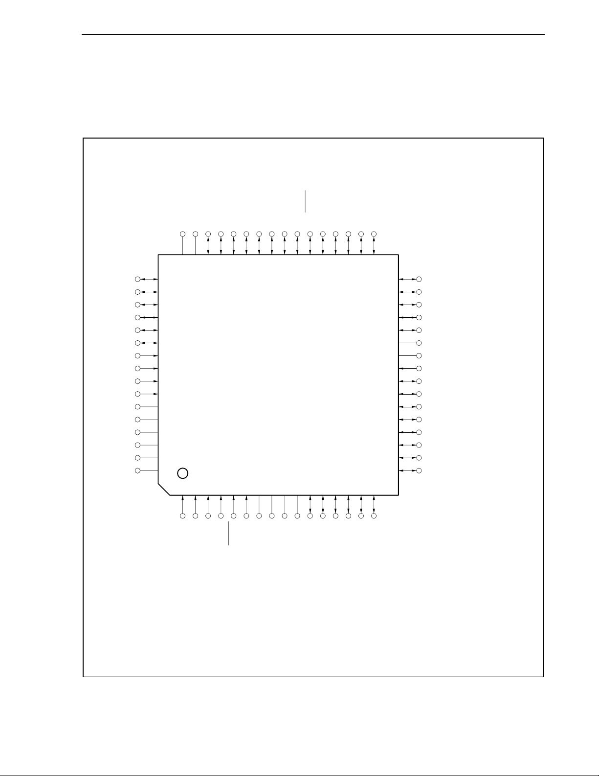
1.5 Pin Configuration
• 64-pin plastic LQFP (14 × 14)
μ
PD70F3713GC-8BS-A
μ
PD70F3714GC-8BS-A
CHAPTER 1 INTRODUCTION
Top View
P25/TOQ1B3
P24/TOQ1T3
P23/TOQ1B2
P22/TOQ1T2
P21/TOQ1B1
P20/TOQ1T1
ANI13
ANI12
ANI11
ANI10
AV
REF1
AV
DD1
AV
SS1
AV
SS0
AV
DD0
AV
REF0
EVSSEVDDP26/TOQ10
484746454443424140393837363534
49
50
51
52
53
54
55
56
57
58
59
60
61
62
63
64
1
2
P27/TOP31
3
4
P30/RXDA0
P31/TXDA0
P32/RXDA1
5
6
7
P33/TXDA1
P40/SIB0
P41/SOB0
P42/SCKB0
8
9
10111213141516
P43/TOP00/TIP00
P44/TOP01/TIP01
PDL0
PDL1
PDL2
33
32
31
30
29
28
27
26
25
24
23
22
21
20
19
18
17
PDL3
PDL4
PDL5/FLMD1
PDL6
PDL7
EV
SS
EV
DD
FLMD0
P10/TOQH01/TIQ01/TOQ01
P11/TIQ02/TOQ02
P12/TOQH02/TIQ03/TOQ03
P13/TIQ00
P14/TOQH03/EVTQ0
P16(CLMER)
P17/TOP21/TIP21
P00/INTP0/TOQH0OFF
Note
/TOQ00(CLMER)
Note
/TIP20
SS
X2
DD
V
V
REGC
P06/INTP6
P05/INTP5/ADTRG1
P04/INTP4/ADTRG0
P03/INTP3/TOP3OFF
P02/INTP2/TOP2OFF
P01/INTP1/TOQ1OFF
ANI00
ANI01
ANI02
ANI03
X1
RESET
Note The CLMER signal is enabled only when P16 is specified as an output port or the output function of
TOQ00. When an error (oscillator stop) is detected by the clock monitor, a low level is forcibly output.
Low-level output is released by reset signal. For details, see Table 4-5 Alternate-Function Pins of
Port 1.
User’s Manual U17716EJ2V0UD
17
Page 18

CHAPTER 1 INTRODUCTION
Pin Identification
ADTRG0, ADTRG1: A/D trigger input SCKB0: Serial clock
ANI00 to ANI03, SIB0: Serial input
ANI10 to ANI13: Analog input SOB0: Serial output
AV
DD0, AVDD1: Analog power supply TIP00, TIP01,
AV
REF0, AVREF1: Analog reference voltage TIP20, TIP21,
AV
SS0, AVSS1: Analog ground TIQ00 to TIQ03: Timer trigger input
EVDD: Power supply for port TOP00, TOP01,
EV
SS: Ground for port TOP21, TOP31,
EVTQ0: Timer event count input TOQ1B1 to TOQ1B3,
FLMD0, FLMD1: Flash programming mode TOQ1T1 to TOQ1T3,
INTP0 to INTP6: External interrupt input TOQ00 to TOQ03,
P00 to P06: Port 0 TOQ10,
P10 to P14, P16, P17: Port 1 TOQH01 to TOQH03: Timer output
P20 to P27: Port 2 TOP2OFF, TOP3OFF,
P30 to P33: Port 3 TOQ1OFF, TOQH0OFF: Timer output off
P40 to P44: Port 4 TXDA0, TXDA1: Transmit data
PDL0 to PDL7: Port DL V
REGC: Regulator control V
DD: Power supply
SS: Ground
RESET: Reset X1, X2: Clock oscillator pin
RXDA0, RXDA1: Receive data
18
User’s Manual U17716EJ2V0UD
Page 19
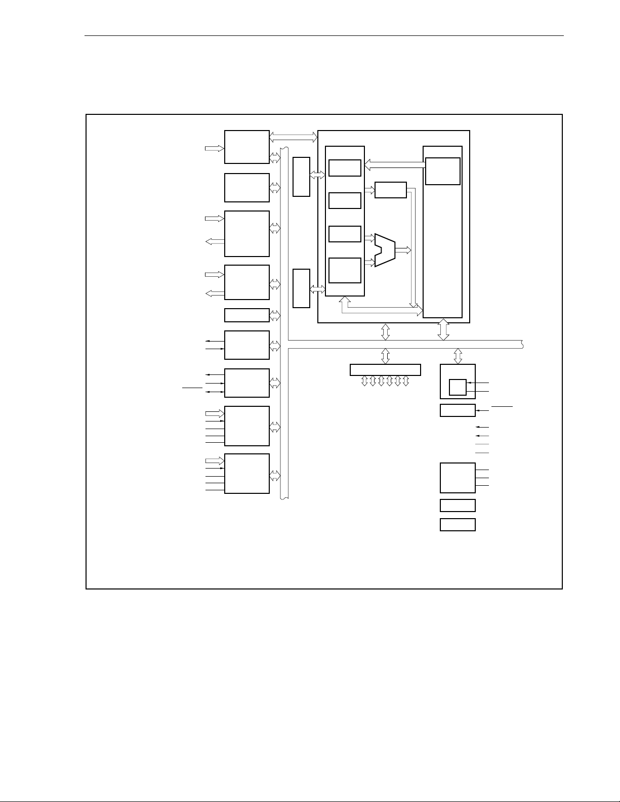
1.6 Function Blocks
(1) Internal block diagram
INTP0 to INTP6
TIQ00 to TIQ03, EVTQ0,
TOQ1OFF, TOQH0OFF
TOQ00 to TOQ03, TOQ10,
TOQH01 to TOQH03,
TOQ1T1 to TOQ1T3,
TOQ1B1 to TOQ1B3
TIP00, TIP01, TIP20,TIP21,
TOP2OFF, TOP3OFF
TOP00, TOP01,
TOP21,TOP31
CHAPTER 1 INTRODUCTION
INTC
TMM
× 1 ch
TMQ
× 2 ch
TMP
× 4 ch
WDT
ROM
Note
RAM
6 KB
PC
32-bit
barrel shifter
System
registers
Generalpurpose
registers
(32 bits
×
32)
CPU
Multiplier
(16 × 16 → 32)
ALU
BCU
Instruction
queue
TXDA0, TXDA1
RXDA0, RXDA1
SOB0
SIB0
SCKB0
ANI00 to ANI03
ADTRG0
AV
REF0
AV
DD0
AV
SS0
ANI10 to ANI13
ADTRG1
AV
REF1
AV
DD1
AV
SS1
UARTA
× 2 ch
CSIB
ADC0
ADC1
Port
P00 to P06
P20 to P27
P30 to P33
P40 to P44
PDL0 to PDL7
P10 to P14, P16, P17
CG
PLL
RG
Regulator
CLM
POC/LVI
X1
X2
RESET
FLMD0
FLMD1
EV
DD
EV
SS
V
DD
V
SS
REGC
Note
μ
PD70F3713: 64 KB (flash memory)
μ
PD70F3714: 128 KB (flash memory)
User’s Manual U17716EJ2V0UD
19
Page 20

(2) Internal units
(a) CPU
The CPU uses five-stage pipeline control to enable single-clock execution of address calculations,
arithmetic logic operations, data transfers, and almost all other instruction processing.
Other dedicated on-chip hardware, such as a multiplier (16 bits × 16 bits → 32 bits) and a barrel shifter (32
bits), help accelerate complex processing.
(b) Bus control unit (BCU)
The BCU controls the internal bus.
(c) ROM
This is flash memory that is mapped from address 00000000H.
During instruction fetch, ROM/flash memory can be accessed from the CPU in 1-clock cycles. The
internal ROM capacity and area differ as follows depending on the product.
μ
PD70F3713 64 KB (flash memory) xn000000H to xn00FFFFH
μ
PD70F3714 128 KB (flash memory) xn000000H to xn01FFFFH
CHAPTER 1 INTRODUCTION
Part Number Internal ROM Capacity Internal ROM Area
Remark n = xx11B
(d) RAM
This is a 6 KB internal RAM that is mapped to the addresses xnFFD800H to xnFFEFFFH.
During instruction fetch or data access, data can be accessed from the CPU in 1-clock cycles.
Remark n = xx11B
(e) Interrupt controller (INTC)
This controller handles hardware interrupt requests (INTP0 to INTP6) from on-chip peripheral hardware
and external hardware. Eight levels of interrupt priorities can be specified for these interrupt requests, and
multiple-interrupt servicing control can be performed.
(f) Clock generator (CG)
The clock generator includes two basic operation modes: PLL mode (fixed to multiplication by eight) and
clock-through mode. It generates four types of clocks (f
the operating clock for the CPU (f
(g) Timer/counter
This unit incorporates one 16-bit interval timer M (TMM) channel, two 16-bit timer/event counter Q (TMQ)
channels, and four 16-bit timer/event counter P (TMP) channels, and can measure pulse interval widths or
frequency, enable an inverter function for motor control, and output a programmable pulse.
(h) Watchdog timer (WDT)
A watchdog timer is equipped to detect program loops, system abnormalities, etc.
It generates a non-maskable interrupt request signal (INTWDT) or internal reset signal (WDTRES) after an
overflow occurs.
XX, fXX/2, fXX/4, fXX/8), and supplies one of them as
CPU).
20
User’s Manual U17716EJ2V0UD
Page 21
CHAPTER 1 INTRODUCTION
(i) Serial interface
The V850ES/IE2 includes two asynchronous serial interface A (UARTA) channels and one 3-wire variable
length serial I/O (CSIB) channel as the serial interface.
For UARTA, data is transferred via the TXDAn and RXDAn pins (n = 0, 1).
For CSIB, data is transferred via the SOB0, SIB0, and SCKB0 pins.
(j) A/D converter (ADC)
The V850ES/IE2 includes two-channel 10-bit A/D converters (ADC0 and ADC1) with four analog input
pins.
(k) Ports
As shown below, the following ports have general-purpose port functions and control pin functions.
Port I/O Alternate Function
Port 0 7-bit I/O Timer/counter input, external interrupt input, external trigger input of A/D converter
Port 1 7-bit I/O Timer/counter I/O
Port 2 8-bit I/O Timer/counter output
Port 3 4-bit I/O Serial interface I/O
Port 4 5-bit I/O Serial interface I/O, timer/counter I/O
Port DL 8-bit I/O
−
User’s Manual U17716EJ2V0UD
21
Page 22
CHAPTER 2 PIN FUNCTIONS
2.1 List of Pin Functions
The names and functions of the pins in the V850ES/IE2 are listed below. These pins can be divided into port pins
and non-port pins according to their function.
There are two power supplies for the I/O buffer of a pin: power supply for A/D converter (AV
power supply for external pin (EVDD). The relationship between each power supply and the pins is shown below.
Table 2-1. I/O Buffer Power Supplies for Each Pin
Power Supply Corresponding Pins
AVDD0, AVDD1 ANI00 to ANI03, ANI10 to ANI13
EVDD Ports 0 to 4, port DL, RESET
(1) Port pins
Pin Name Pin No. I/O Function Alternate Function
P00 17 INTP0/TOQH0OFF
P01 16 INTP1/TOQ1OFF
P02 15 INTP2/TOP2OFF
P03 14 INTP3/TOP3OFF
P04 13 INTP4/ADTRG0
P05 12 INTP5/ADTRG1
P06 11
P10 24 TOQH01/TIQ01/TOQ01
P11 23 TIQ02/TOQ02
P12 22 TOQH02/TIQ03/TOQ03
P13 21 TIQ00
P14 20 TOQH03/EVTQ0
P16
(CLMER)
P17 18
Note
19 TOQ00 (CLMER)
I/O Port 0
7-bit I/O port
Input data read/output data write is enabled in 1-bit units.
Use of an on-chip pull-up resistor can be specified in 1-bit
units (the on-chip pull-up resistor can be connected only in
the input mode of the port mode and when the alternate
function of the pin is used).
I/O Port 1
7-bit I/O port
Input data read/output data write is enabled in 1-bit units.
Use of an on-chip pull-up resistor can be specified in 1-bit
units (the on-chip pull-up resistor can be connected only in
the input mode of the port mode, when the input mode of
alternate function of the pin is used, and when TOP21 and
TOQH01 to TOQH03 pins, which function as output pins
when their alternate function is used, go into a highimpedance state).
INTP6
TOP21/TIP21
DD0 and AVDD1) and
Note
/TIP20
(1/2)
Note The CLMER signal is enabled only when P16 is specified as an output port or the output function of
TOQ00. When an error (oscillator stop) is detected by the clock monitor, a low level is forcibly output.
Low-level output is released by reset signal. For details, see Table 4-5 Alternate-Function Pins of Port
1.
22
User’s Manual U17716EJ2V0UD
Page 23
<R>
CHAPTER 2 PIN FUNCTIONS
Pin Name Pin No. I/O Function Alternate Function
P20 54 TOQ1T1
P21 53 TOQ1B1
P22 52 TOQ1T2
P23 51 TOQ1B2
P24 50 TOQ1T3
P25 49 TOQ1B3
P26 46 TOQ10
P27 45
P30 44 RXDA0
P31 43 TXDA0
P32 42 RXDA1
P33 41
P40 40 SIB0
P41 39 SOB0
P42 38 SCKB0
P43 37 TOP00/TIP00
P44 36
PDL0 35
PDL1 34
PDL2 33
PDL3 32
PDL4 31
PDL5 30 FLMD1
PDL6 29
PDL7 28
I/O Port 2
8-bit I/O port
Input data read/output data write is enabled in 1-bit units.
Use of an on-chip pull-up resistor can be specified in 1-bit
units (the on-chip pull-up resistor can be connected only in
the input mode of the port mode, or when TOQ1T1 to
TOQ1T3 and TOQ1B1 to TOQ1B3 and TOP31 pins, which
function as output pins when their alternate function is used,
go into a high-impedance state).
I/O Port 3
4-bit I/O port
Input data read/output data write is enabled in 1-bit units.
Use of an on-chip pull-up resistor can be specified in 1-bit
units (the on-chip pull-up resistor can be connected only in
the input mode of the port mode and when the input mode of
the alternate function of the pin is used).
I/O Port 4
5-bit I/O port
Input data read/output data write is enabled in 1-bit units.
An on-chip pull-up resistor can be specified in 1-bit units (the
on-chip pull-up resistor can be connected only in the input
mode of the port mode, including the case where the SCKB0
pin in the slave mode, and when the alternate function of the
pin is used in the input mode).
I/O Port DL
8-bit I/O port
Input data read/output data write is enabled in 1-bit units.
An on-chip pull-up resistor can be specified in 1-bit units
(the on-chip pull-up resistor can be connected when the
pins are in the port mode and input mode).
TOP31
TXDA1
TOP01/TIP01
−
−
−
−
−
−
−
(2/2)
User’s Manual U17716EJ2V0UD
23
Page 24
CHAPTER 2 PIN FUNCTIONS
(2) Non-port pins
(1/2)
Pin Name Pin No. I/O Function Alternate Function
ADTRG0 13 Input INTP4/P04
ADTRG1 12 Input
ANI00
ANI01
ANI02
ANI03
ANI10
ANI11
ANI12
ANI13
AVDD0
AVDD1
AVREF0
AVREF1
AVSS0
AVSS1
EVDD
EVSS
1
2
3
4
58
57
56
55
63
60
64
59
62
61
26, 47
27, 48
Input
Input
Input
Input
Input
Input
Input
Input
External trigger input for A/D converters 0, 1
INTP5/P05
Analog input to A/D converters 0, 1
− −
Positive power supply for A/D converters 0, 1 (same
potential as V
−
− −
Reference voltage input for A/D converters 0, 1 (same
potential as AV
−
− −
Ground potential for A/D converters 0, 1 (same potential
SS)
as V
−
−
Positive power supply for external pin
Ground potential for external pin
−
DD)
DD0 and AVDD1)
−
−
−
−
−
−
−
−
−
−
−
−
−
EVTQ0 20 Input External event count input of TMQ0 TOQH03/P14
FLMD0 25 Input
FLMD1 30 Input
INTP0 17 TOQH0OFF/P00
Input External maskable interrupt request input
Pin for setting flash memory programming mode
−
PDL5
INTP1 16 TOQ1OFF/P01
INTP2 15 TOP2OFF/P02
INTP3 14 TOP3OFF/P03
INTP4 13 ADTRG0/P04
INTP5 12 ADTRG1/P05
INTP6 11
REGC 10 − Regulator output stabilization capacitance connection
RESET 5 Input System reset input
RXDA0 44 P30
Input Serial receive data input of UARTA0, UARTA1
RXDA1 42
P06
−
−
P32
SCKB0 38 I/O Serial clock I/O of CSIB0 P42
SIB0 40 Input Serial receive data input of CSIB0 P40
SOB0 39 Output Serial transmit data output of CSIB0 P41
24
User’s Manual U17716EJ2V0UD
Page 25

CHAPTER 2 PIN FUNCTIONS
Pin Name Pin No. I/O Function Alternate Function
TIP00 37
Input
External event count input/external trigger input/capture
TOP00/P43
trigger input of TMP0
TIP01 36 Capture trigger input of TMP0 TOP01/P44
TIP20 19
External event count input/external trigger input/capture
trigger input of TMP2
TIP21 18
TIQ00 21 P13
Input Capture trigger input of TMQ0
Capture trigger input of TMP2 TOP21/P17
TOQ00 (CLMER)
P16 (CLMER)
Note
TIQ01 24 TOQH01/TOQ01/P10
TIQ02 23 TOQ02/P11
TIQ03 22
TOP00 37 TIP00/P43
Output Pulse signal output of TMP0, TMP2
TOQH02/TOQ03/P12
TOP01 36 TIP01/P44
TOP21 18
TIP21/P17
TOP2OFF 15 Input High-impedance output control signal input INTP2/P02
TOP31 45 Output Pulse signal output of TMP3 P27
TOP3OFF 14 Input High-impedance output control signal input INTP3/P03
TOQ00 (CLMER)
Note
19 TIP20/P16 (CLMER)
Output Pulse signal output of TMQ0
TOQ01 24 TOQH01/TIQ01/P10
TOQ02 23 TIQ02/P11
TOQ03 22
TOQH02/TIQ03/P12
TOQ10 46 Output Pulse signal output of TMQ1 P26
TOQ1B1 53 P21
Output Pulse signal output for 6-phase PWM
TOQ1B2 51 P23
TOQ1B3 49
P25
TOQ1OFF 16 Input High-impedance output control signal input INTP1/P01
TOQ1T1 54 P20
Output Pulse signal output for 6-phase PWM
TOQ1T2 52 P22
TOQ1T3 50
TOQH01 24 TIQ01/TOQ01/P10
Output
TOQH02 22 TIQ03/TOQ03/P12
High-impedance output by TMQ0 pulse signal output and
valid edge of TOQH0OFF pin input
TOQH03 20
P24
EVTQ0/P14
TOQH0OFF 17 Input High-impedance output control signal input INTP0/P00
TXDA0 43 P31
TXDA1 41
VDD 9
VSS 8
X1 6 Input
X2 7
Output Serial transmit data output of UARTA0, UARTA1
Positive power supply for internal unit
−
Ground potential for internal unit
−
Resonator connection pin for system clock
−
P33
−
−
−
−
Note The CLMER signal is enabled only when P16 is specified as an output port or the output function of
TOQ00. When an error (oscillator stop) is detected by the clock monitor, a low level is forcibly output.
Low-level output is released by reset signal. For details, see Table 4-5 Alternate-Function Pins of Port
1.
(2/2)
Note
/
Note
User’s Manual U17716EJ2V0UD
25
Page 26
CHAPTER 2 PIN FUNCTIONS
2.2 Pin I/O Circuits and Recommended Connection of Unused Pins
Pin Name Alternate-Function Pin Name Pin No. I/O Circuit
Type
P00 INTP0/TOQH0OFF
17
8-P
Input: Independently connect to EV
P01 INTP1/TOQ1OFF 16
P02 INTP2/TOP2OFF 15
Output: Leave open.
P03 INTP3/TOP3OFF 14
P04 INTP4/ADTRG0 13
P05 INTP5/ADTRG1 12
P06 INTP6 11
P10 TOQH01/TIQ01/TOQ01 24
P11 TIQ02/TOQ02 23
P12 TOQH02/TIQ03/TOQ03 22
P13 TIQ00 21
P14 TOQH03/EVTQ0 20
P16 (CLMER)
Note
TOQ00 (CLMER)
Note
/TIP20 19
P17 TOP21/TIP21 18
P20 TOQ1T1 54
5-AG
P21 TOQ1B1 53
P22 TOQ1T2 52
P23 TOQ1B2 51
P24 TOQ1T3 50
P25 TOQ1B3 49
P26 TOQ10 46
P27 TOP31 45
P30 RXDA0 44 8-P
P31 TXDA0 43 5-AG
P32 RXDA1 42 8-P
P33 TXDA1 41 5-AG
P40 SIB0 40 8-P
P41 SOB0 39 5-AG
P42 SCKB0 38
8-P
P43 TOP00/TIP00 37
P44 TOP01/TIP01 36
Note The CLMER signal is enabled only when P16 is specified as an output port or the output function of
TOQ00. When an error (oscillator stop) is detected by the clock monitor, a low level is forcibly output.
Low-level output is released by reset signal. For details, see Table 4-5 Alternate-Function Pins of Port
1.
Recommended Connection
EV
SS via a resistor.
(1/2)
DD or
26
User’s Manual U17716EJ2V0UD
Page 27
CHAPTER 2 PIN FUNCTIONS
Pin Name Alternate-Function Pin Name Pin No. I/O Circuit
Type
PDL0
PDL1
PDL2
PDL3
PDL4
−
−
−
−
−
35
34
33
32
31
5-AG
PDL5 FLMD1 30
PDL6
PDL7
ANI00
ANI01
ANI02
ANI03
ANI10
ANI11
ANI12
ANI13
RESET
FLMD0
−
−
−
−
−
−
−
−
−
−
−
−
29
28
58
57
56
55
25
1
7
2
3
4
5
2
Recommended Connection
Input: Independently connect to
DD or EVSS via a resistor.
EV
Output: Leave open.
Independently connect to AV
AV
DD1, AVSS0, or AVSS1 via a resistor.
DD0,
−
−
(2/2)
User’s Manual U17716EJ2V0UD
27
Page 28
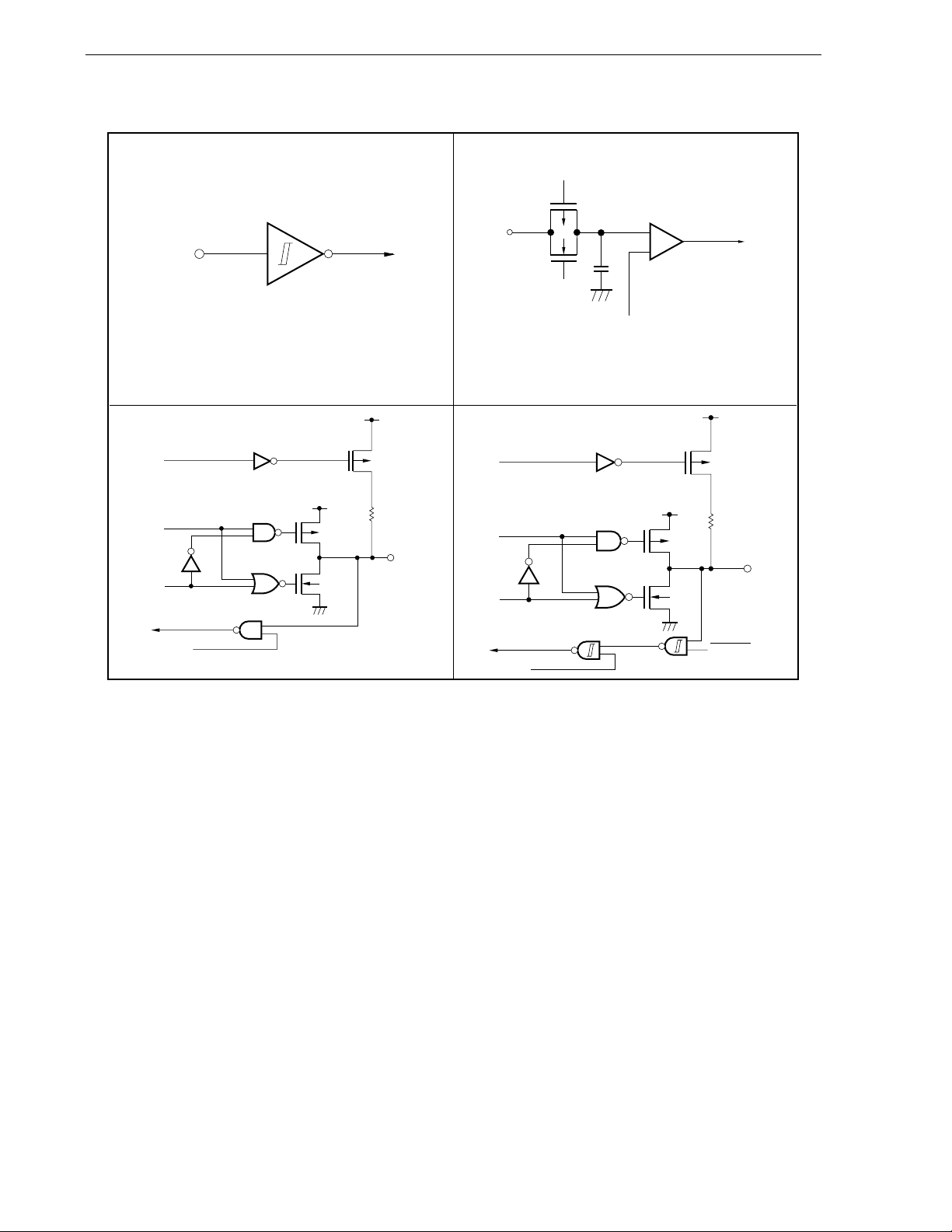
2.3 Pin I/O Circuits
Type 2
CHAPTER 2 PIN FUNCTIONS
Type 7
IN
Schmitt-triggered input with hysteresis characteristics
Type 5-AG
Pull-up
enable
Data
Output
EV
DD
P-ch
N
-ch
EV
P-ch
disable
EV
SS
Input
enable
DD
IN/OUT
IN
AV
Type 8-P
Pull-up
enable
Data
Output
disable
Input enable
P-ch
N
-ch
SS0
, AV
SS1
(Threshold voltage)
Comparator
+
–
V
REF
EV
DD
P-ch
DD
EV
P-ch
IN/OUT
N-ch
EV
SS
RESET
28
User’s Manual U17716EJ2V0UD
Page 29

CHAPTER 3 CPU FUNCTION
The CPU of the V850ES/IE2 is based on the RISC architecture and executes most instructions in one clock cycle
by using 5-stage pipeline control.
3.1 Features
{ Minimum instruction execution time: 50 ns
(@ 20 MHz operation: 4.5 to 5.5 V (when using A/D converter),
3.5 to 5.5 V (when not using A/D converter))
{ Memory space Program (physical address) space: 64 MB linear
Data (logical address) space: 4 GB linear
{ General-purpose registers: 32 bits × 32
{ Internal 32-bit architecture
{ 5-stage pipeline control
{ Multiply/divide instructions
{ Saturated operation instructions
{ 32-bit shift instruction: 1 clock
{ Load/store instruction with long/short format
{ Four types of bit manipulation instructions
• SET1
• CLR1
• NOT1
• TST1
User’s Manual U17716EJ2V0UD
29
Page 30
CHAPTER 3 CPU FUNCTION
3.2 CPU Register Set
The CPU registers of the V850ES/IE2 can be classified into two categories: a general-purpose program register set
and a dedicated system register set. All the registers have 32-bit width.
For details, refer to the V850ES Architecture User’s Manual.
(1) Program register set (2) System register set
31 0 31 0
r0
r1
r2
r3
r4
r5
r6
r7
r8
r9
r10
r11
r12
r13
r14
r15
r16
r17
r18
r19
r20
r21
r22
r23
r24
r25
r26
r27
r28
r29
r30
r31
(Zero register)
(Assembler-reserved register)
(Stack pointer (SP))
(Global pointer (GP))
(Text pointer (TP))
(Element pointer (EP))
(Link pointer (LP))
EIPC
EIPSW
FEPC
FEPSW
ECR (Interrupt source register)
PSW (Program status word)
CTPC
CTPSW
DBPC
DBPSW
CTBP (CALLT base pointer)
(Interrupt status saving register)
(Interrupt status saving register)
(NMI status saving register)
(NMI status saving register)
(CALLT execution status saving register)
(CALLT execution status saving register)
(Exception/debug trap status saving register)
(Exception/debug trap status saving register)
31 0
PC (Program counter)
30
User’s Manual U17716EJ2V0UD
Page 31

CHAPTER 3 CPU FUNCTION
3.2.1 Program register set
The program register set includes general-purpose registers and a program counter.
(1) General-purpose registers (r0 to r31)
Thirty-two general-purpose registers, r0 to r31, are available. All of these registers can be used as a data
variable or address variable.
However, r0 and r30 are implicitly used by instructions and care must be exercised when using these
registers. r0 always holds 0 and is used for operations that use 0 and offset 0 addressing. r30 is used as a
base pointer when performing memory access with the SLD and SST instructions.
Also, r1, r3 to r5, and r31 are implicitly used by the assembler and C compiler. Therefore, before using these
registers, their contents must be saved so that they are not lost, and they must be restored to the registers
after the registers have been used. There are cases when r2 is used by the real-time OS. If r2 is not used by
the real-time OS, r2 can be used as a variable register.
Table 3-1. General-Purpose Registers
Name Usage Operation
r0 Zero register Always holds 0
r1 Assembler-reserved register Working register for generating 32-bit immediate
r2 Address/data variable register (when r2 is not used by the real-time OS to be used)
r3 Stack pointer Used to generate stack frame when function is called
r4 Global pointer Used to access global variable in data area
r5 Text pointer Register to indicate the start of the text area (area for placing program code)
r6 to r29 Address/data variable register
r30 Element pointer Base pointer when memory is accessed
r31 Link pointer Used by compiler when calling function
(2) Program counter (PC)
This register holds the address of the instruction under execution. The lower 26 bits of this register are valid,
and bits 31 to 26 are fixed to 0. If a carry occurs from bit 25 to bit 26, it is ignored.
Bit 0 is fixed to 0, and branching to an odd address cannot be performed.
31 26 25 1 0
PC
Fixed to 0 Instruction address under execution 0
After reset
00000000H
User’s Manual U17716EJ2V0UD
31
Page 32

CHAPTER 3 CPU FUNCTION
3.2.2 System register set
System registers control the status of the CPU and hold interrupt information.
Read from and write to system registers are performed by setting the system register numbers shown below with
the system register load/store instructions (LDSR, STSR instructions).
Table 3-2. System Register Numbers
System
Register No.
0 Interrupt status saving register (EIPC)
1 Interrupt status saving register (EIPSW)
2 NMI status saving register (FEPC) Yes Yes
3 NMI status saving register (FEPSW) Yes Yes
4 Interrupt source register (ECR) No Yes
5 Program status word (PSW) Yes Yes
6 to 15
Reserved numbers for future function expansion (The operation is not guaranteed
if accessed.)
16 CALLT execution status saving register (CTPC) Yes Yes
17 CALLT execution status saving register (CTPSW) Yes Yes
18 Exception/debug trap status saving register (DBPC) Yes
19 Exception/debug trap status saving register (DBPSW) Yes
20 CALLT base pointer (CTBP) Yes Yes
21 to 31
Reserved numbers for future function expansion (The operation is not guaranteed
if accessed.)
System Register Name
Note 1
Yes Yes
Note 1
Yes Yes
Operand Specification Enabled
LDSR
Instruction
STSR
Instruction
No No
Note 2
Yes
Note 2
Yes
Note 2
Note 2
No No
Notes 1. Since only one set of these registers is available, the contents of this register must be saved by the
program when multiple interrupt servicing is enabled.
2. Can be accessed only after the DBTRAP instruction or illegal opcode is executed and before the DBRET
instruction is executed.
Caution Even if bit 0 of EIPC, FEPC, or CTPC is set (1) by the LDSR instruction, bit 0 is ignored during return
with the RETI instruction following interrupt servicing (because bit 0 of PC is fixed to 0). When
setting a value to EIPC, FEPC, and CTPC, set an even number (bit 0 = 0).
32
User’s Manual U17716EJ2V0UD
Page 33

CHAPTER 3 CPU FUNCTION
(1) Interrupt status saving registers (EIPC, EIPSW)
There are two interrupt status saving registers, EIPC and EIPSW.
Upon occurrence of a software exception or a maskable interrupt, the contents of the program counter (PC)
are saved to EIPC and the contents of the program status word (PSW) are saved to EIPSW (upon occurrence
of a non-maskable interrupt (NMI), the contents are saved to the NMI status saving registers (FEPC,
FEPSW)).
The address of the next instruction following the instruction executed when a software exception or maskable
interrupt occurs is saved to EIPC, except for some instructions (see 14.9 Periods in Which CPU Does Not
Acknowledge Interrupts).
The current PSW contents are saved to EIPSW.
Since there is only one set of interrupt status saving registers, the contents of these registers must be saved
by the program when multiple interrupt servicing is enabled.
Bits 31 to 26 of EIPC and bits 31 to 8 of EIPSW are reserved (fixed to 0) for future function expansion.
When the RETI instruction is executed, the values in EIPC and EIPSW are restored to the PC and PSW,
respectively.
31 0
EIPC
31 0
EIPSW
26 25
0 0 0 0
0 0 0 0 00 0 0 0 0 00 0 0 0 0 00 0 0 0 0
(PC contents saved)00
After reset
0xxxxxxxH
(x: Undefined)
7
8
(PSW contents saved)00
After reset
000000xxH
(x: Undefined)
User’s Manual U17716EJ2V0UD
33
Page 34

CHAPTER 3 CPU FUNCTION
(2) NMI status saving registers (FEPC, FEPSW)
There are two NMI status saving registers, FEPC and FEPSW.
Upon occurrence of a non-maskable interrupt (NMI), the contents of the program counter (PC) are saved to
FEPC and the contents of the program status word (PSW) are saved to FEPSW.
The address of the next instruction following the instruction executed when a non-maskable interrupt occurs is
saved to FEPC, except for some instructions.
The current PSW contents are saved to FEPSW.
Bits 31 to 26 of FEPC and bits 31 to 8 of FEPSW are reserved (fixed to 0) for future function expansion.
When the RETI instruction has been executed, the values of FEPC and FEPSW are restored to the PC and
PSW, respectively.
31 0
FEPC
31 0
FEPSW
26 25
0 0 0 0
0 0 0 0 00 0 0 0 0 00 0 0 0 0 00 0 0 0 0
(PC contents saved)00
After reset
0xxxxxxxH
(x: Undefined)
7
8
(PSW contents saved)00
After reset
000000xxH
(x: Undefined)
(3) Interrupt source register (ECR)
Upon occurrence of an interrupt or an exception, the interrupt source register (ECR) holds the source of an
interrupt or an exception. The value held by ECR is the exception code coded for each interrupt source. This
register is a read-only register, and thus data cannot be written to it using the LDSR instruction.
ECR
31 0
FECC EICC
16 15
After reset
00000000H
Bit position Bit name Description
31 to 16 FECC Non-maskable interrupt (NMI) exception code
15 to 0 EICC Exception, maskable interrupt exception code
34
User’s Manual U17716EJ2V0UD
Page 35

CHAPTER 3 CPU FUNCTION
(4) Program status word (PSW)
The program status word (PSW) is a collection of flags that indicate the program status (instruction execution
result) and the CPU status.
When the contents of this register are changed using the LDSR instruction, the new contents become valid
immediately following completion of LDSR instruction execution. Interrupt request acknowledgment is held
pending while a write to the PSW is being executed by the LDSR instruction.
Bits 31 to 8 are reserved (fixed to 0) for future function expansion.
(1/2)
31 0
PSW
RFU
Bit position Flag name Description
31 to 8 RFU Reserved field. Fixed to 0.
7 NP
6 EP
5 ID
4 SAT
3 CY
Note
Note
2 OV
1 S
0 Z
Note
Indicates that non-maskable interrupt (NMI) servicing is in progress. This flag is set to 1 when
an NMI request is acknowledged, and disables multiple interrupts.
0: NMI servicing not in progress
1: NMI servicing in progress
Indicates that exception processing is in progress. This flag is set to 1 when an exception
occurs. Moreover, interrupt requests can be acknowledged even when this bit is set.
0: Exception processing not in progress
1: Exception processing in progress
Indicates whether maskable interrupt request acknowledgment is enabled.
0: Interrupt enabled (EI)
1: Interrupt disabled (DI)
Indicates that the result of executing a saturated operation instruction has overflowed and that
the calculation result is saturated. Since this is a cumulative flag, it is set to 1 when the result of
a saturated operation instruction becomes saturated, and it is not cleared to 0 even if the
operation results of successive instructions do not become saturated. This flag is neither set
nor cleared when arithmetic operation instructions are executed.
0: Not saturated
1: Saturated
Indicates whether carry or borrow occurred as the result of an operation.
0: No carry or borrow occurred
1: Carry or borrow occurred
Indicates whether overflow occurred during an operation.
0: No overflow occurred
1: Overflow occurred.
Indicates whether the result of an operation is negative.
0: Operation result is positive or 0.
1: Operation result is negative.
Indicates whether operation result is 0.
0: Operation result is not 0.
1: Operation result is 0.
Remark Note is explained on the following page.
87NP6EP5ID4
SAT3CY2OV
1
SZ
After reset
00000020H
User’s Manual U17716EJ2V0UD
35
Page 36

CHAPTER 3 CPU FUNCTION
(2/2)
Note During saturated operation, the saturated operation results are determined by the contents of the OV
flag and S flag. The SAT flag is set (to 1) only when the OV flag is set (to 1) during saturated operation.
Flag status
Maximum positive value exceeded 1 1 0 7FFFFFFFH
Maximum negative value exceeded 1 1 1 80000000H
Positive (maximum value not exceeded) 0
Negative (maximum value not exceeded)
Operation result status
SAT OV S
Holds value
before operation
0
1
Saturated
operation result
Actual operation
result
(5) CALLT execution status saving registers (CTPC, CTPSW)
There are two CALLT execution status saving registers, CTPC and CTPSW.
When the CALLT instruction is executed, the contents of the program counter (PC) are saved to CTPC, and
the program status word (PSW) contents are saved to CTPSW.
The contents saved to CTPC consist of the address of the next instruction after the CALLT instruction.
The current PSW contents are saved to CTPSW.
Bits 31 to 26 of CTPC and bits 31 to 8 of CTPSW are reserved (fixed to 0) for future function expansion.
31 0
CTPC
31 0
CTPSW
26 25
0 0 0 0
0 0 0 0 00 0 0 0 0 00 0 0 0 0 00 0 0 0 0
(PC contents saved)00
After reset
0xxxxxxxH
(x: Undefined)
7
8
(PSW contents saved)00
After reset
000000xxH
(x: Undefined)
36
User’s Manual U17716EJ2V0UD
Page 37

<R>
CHAPTER 3 CPU FUNCTION
(6) Exception/debug trap status saving registers (DBPC, DBPSW)
There are two exception/debug trap status saving registers, DBPC and DBPSW.
Upon occurrence of an exception trap or debug trap, the contents of the program counter (PC) are saved to
DBPC, and the program status word (PSW) contents are saved to DBPSW.
The contents saved to DBPC consist of the address of the next instruction after the instruction executed when
an exception trap or debug trap occurs.
The current PSW contents are saved to DBPSW.
These registers can be read or written only in the period between DBTRAP instruction or illegal opcode
execution and DBRET instruction execution.
Bits 31 to 26 of DBPC and bits 31 to 8 of DBPSW are reserved (fixed to 0) for future function expansion.
When the DBRET instruction has been executed, the values of DBPC and DBPSW are restored to the PC and
PSW, respectively.
31 0
DBPC
31 0
DBPSW
26 25
0 0 0 0
0 0 0 0 00 0 0 0 0 00 0 0 0 0 00 0 0 0 0
(Saved PC contents) 00
(x: Undefined)
7
8
(Saved PSW contents) 00
000000xxH
(x: Undefined)
(7) CALLT base pointer (CTBP)
The CALLT base pointer (CTBP) is used to specify table addresses and generate target addresses (bit 0 is
fixed to 0).
Bits 31 to 26 are reserved (fixed to 0) for future function expansion.
31 0
CTBP
26 25
0 0 0 0 0
(Base address) 00
After reset
0xxxxxxxH
(x: Undefined)
After reset
0xxxxxxxH
After reset
User’s Manual U17716EJ2V0UD
37
Page 38

CHAPTER 3 CPU FUNCTION
3.3 Operating Modes
The V850ES/IE2 has the following operating modes.
(1) Normal operating mode
After the system has been released from the reset state, the pins related to the bus interface are set to the port
mode, execution branches to the reset entry address of the internal ROM, and instruction processing is
started.
(2) Flash memory programming mode
When this mode is set, a program can be written to the internal flash memory by the flash memory
programmer.
(a) Operating mode specification
The operating mode is specified according to the status (input level) of the FLMD0 and FLMD1 pins.
In the normal operating mode, input a low level to the FLMD0 pin after reset.
When the flash memory programmer is connected, a high level is input to the FLMD0 pin by the flash
memory programmer in the flash memory programming mode; however, in the self-programming mode,
input a high level via an external circuit.
Fix the specifications of these pins in the application system, and do not change then during operation.
FLMD0 FLMD1 Operating Mode
L
H L
H H
×
Normal operating mode
Flash memory programming mode
Setting prohibited
H: High level
L: Low level
×: Don’t care
38
User’s Manual U17716EJ2V0UD
Page 39

CHAPTER 3 CPU FUNCTION
3.4 Address Space
3.4.1 CPU address space
For instruction addressing, an internal ROM area of up to 1 MB, and an internal RAM area are supported in a linear
address space (program space) of up to 64 MB. For operand addressing (data access), up to 4 GB of a linear
address space (data space) is supported. The 4 GB address space, however, is viewed as 64 images of a 64 MB
physical address space. This means that the same 64 MB physical address space is accessed regardless of the value
of bits 31 to 26.
Figure 3-1. Address Space Image
Image 63
Program space
Reserved area
Internal RAM area
Access-prohibited area
4 GB
64 MB
•
•
•
Image 1
Image 0
Data space
On-chip peripheral I/O area
Internal RAM area
64 MB
Access-prohibited area
Internal ROM area
1 MB
Internal ROM area
(external memory)
User’s Manual U17716EJ2V0UD
39
Page 40

CHAPTER 3 CPU FUNCTION
3.4.2 Wraparound of CPU address space
(1) Program space
Of the 32 bits of the program counter (PC), the higher 6 bits are fixed to 0 and only the lower 26 bits are valid.
Even if a carry or borrow occurs from bit 25 to bit 26 as a result of branch address calculation, the higher 6 bits
ignore this and remain 0.
Therefore, the upper-limit address of the program space, 03FFFFFFH, and the lower-limit address,
00000000H, are contiguous addresses, and the program space is wrapped around at the boundary of these
addresses.
Caution No instructions can be fetched from the 4 KB area of 03FFF000H to 03FFFFFFH because this
area is an on-chip peripheral I/O area. Therefore, do not execute any branch operation
instructions in which the destination address will reside in any part of this area.
00000001H
00000000H
03FFFFFFH
03FFFFFEH
Program space
(+) direction (–) direction
Program space
(2) Data space
The result of an operand address calculation that exceeds 32 bits is ignored.
Therefore, the upper-limit address of the data space, FFFFFFFFH, and the lower-limit address, 00000000H,
are contiguous addresses, and the data space is wrapped around at the boundary of these addresses.
00000001H
Data space
40
00000000H
(+) direction (–) direction
FFFFFFFFH
FFFFFFFEH
Data space
User’s Manual U17716EJ2V0UD
Page 41

CHAPTER 3 CPU FUNCTION
3.4.3 Memory map
The V850ES/IE2 has reserved areas as shown below.
Figure 3-2. Data Memory Map (Physical Addresses)
3FFFFFFH
(80 KB)
3FEC000H
3FEBFFFH
On-chip peripheral I/O area
(4 KB)
Internal RAM area
(60 KB)
Access-prohibited area
3FFFFFFH
3FFF000H
3FFEFFFH
3FF0000H
3FEFFFFH
3FEC000H
Access-prohibited area
01FFFFFH
Access-prohibited area
0200000H
01FFFFFH
0000000H
(2 MB)
Internal ROM area
(1 MB)
0100000H
00FFFFFH
0000000H
User’s Manual U17716EJ2V0UD
41
Page 42

CHAPTER 3 CPU FUNCTION
Figure 3-3. Program Memory Map
03FFFFFFH
03FFF000H
03FFEFFFH
3FF0000H
3FEFFFFH
Access-prohibited area
(program fetch disabled area)
Internal RAM area
(60 KB)
Access-prohibited area
(program fetch disabled area)
00100000H
000FFFFFH
00000000H
Internal ROM area
(1 MB)
42
User’s Manual U17716EJ2V0UD
Page 43

CHAPTER 3 CPU FUNCTION
3.4.4 Areas
(1) Internal ROM area
An area of 1 MB from 0000000H to 00FFFFFH is reserved for the internal ROM area.
(a) Internal ROM (128 KB)
A 128 KB area from 0000000H to 001FFFFH is provided in the
μ
PD70F3714.
Addresses 0020000H to 00FFFFFH are an access-prohibited area.
Figure 3-4. Internal ROM Area (128 KB)
00FFFFFH
Access-prohibited
area
0020000H
001FFFFH
(b) Internal ROM (64 KB)
A 64 KB area from 000000H to 000FFFFH is provided in the
Addresses 0010000 to 00FFFFFH are an access-prohibited area.
Internal ROM area
(128 KB)
0000000H
μ
PD70F3713.
Figure 3-5. Internal ROM Area (64 KB)
00FFFFFH
Access-prohibited
area
0010000H
000FFFFH
0000000H
Internal ROM area
(64 KB)
User’s Manual U17716EJ2V0UD
43
Page 44

CHAPTER 3 CPU FUNCTION
(2) Internal RAM area
An area of 60 KB maximum from 3FF0000H to 3FFEFFFH is reserved for the internal RAM area.
A 6 KB area from 3FFD800H to 3FFEFFFH is provided as physical internal RAM for the V850ES/IE2.
Addresses 3FF0000H to 3FFD7FFH are an access-prohibited area.
Figure 3-6. Internal RAM Area (6 KB)
Physical address space
Logical address space
3FFEFFFH
Internal RAM (6 KB)
3FFD800H
3FFD7FFH
Access-prohibited area
3FF0000H
FFFEFFFH
FFFD800H
FFFD7FFH
FFF0000H
44
User’s Manual U17716EJ2V0UD
Page 45

(c) Internal memory size setting register (IMS)
The IMS register is used to set the internal RAM size of the V850ES/IE2.
This register is write-only, in 8-bit units.
Reset sets this register to 00H.
Cautions 1. Write the IMS register before the internal RAM is accessed. This register can be
written only once after reset has been released.
2. Be sure to write 01H to the IMS register.
3. The sample startup routine supplied with the CA850 includes a code that clears the
internal RAM area to 0. Therefore, setting the IMS register is required before the
zero-clear routine is executed.
When using the sample startup routine, add instructions <2> to <5> shown in
[Description example] below immediately after the __START label in the startup
routine.
“0x11” of instruction <2> is the set value of the VSWC register and “0x01” of
instruction <4> is the set value of the IMS register.
[Description example]
CHAPTER 3 CPU FUNCTION
<1>_ _START:
<2>mov 0x11, r13
<3>st.b r13, VSWC
<4>mov 0x01, r12
Add
<5>st.b r12, IMS
<6>mov #_tp_TEXT, tp
:
:
Remark When using a partner tool, make the setting in accordance with the contents of Cautions 1 to 3.
Moreover, describe as follows to define the IMS register.
#define IMS (*((volatile unsigned char *)0xfffff9f0))
After reset: 00H W Address: FFFFF9F0H
IMS 0 0 0 0 0 0 RAM0
0
RAM0
0
1
Specification of internal RAM size
Undefined
6 KB (3FFD800H to 3FFEFFFH (RAM size of V850ES/IE2))
User’s Manual U17716EJ2V0UD
45
Page 46

CHAPTER 3 CPU FUNCTION
(3) On-chip peripheral I/O area
A 4 KB area from 3FFF000H to 3FFFFFFH is reserved as the on-chip peripheral I/O area.
Figure 3-7. On-Chip Peripheral I/O Area
Physical address space
Logical address space
3FFFFFFH
On-chip peripheral I/O area
(4 KB)
3FFF000H
FFFFFFFH
FFFF000H
On-chip peripheral I/O registers assigned with functions such as on-chip peripheral I/O operation mode
specification and state monitoring are mapped to the on-chip peripheral I/O area. Program fetches are not
allowed in this area.
Cautions 1. If word access of a register is attempted, halfword access to the word area is performed
twice, first for the lower bits, then for the higher bits, ignoring the lower 2 address bits.
2. If a register that can be accessed in byte units is accessed in halfword units, the higher 8
bits become undefined if the access is a read operation. If a write access is performed,
only the data in the lower 8 bits is written to the register.
3. Addresses that are not defined as registers are reserved for future expansion. If these
addresses are accessed, the operation is undefined and not guaranteed.
46
User’s Manual U17716EJ2V0UD
Page 47

CHAPTER 3 CPU FUNCTION
3.4.5 Recommended use of address space
The architecture of the V850ES/IE2 requires that a register that serves as a pointer be secured for address
generation when operand data in the data space is accessed. The ±32 KB area of addresses stored in this pointer
can be directly accessed by an instruction for operand data. Because the number of general-purpose registers that
can be used as a pointer is limited, however, by keeping the performance from dropping during address calculation
when a pointer value is changed, as many general-purpose registers as possible can be secured for variables, and
the program size can be reduced.
(1) Program space
Of the 32 bits of the PC (program counter), the higher 6 bits are fixed to 0, and only the lower 26 bits are valid.
Regarding the program space, therefore, a 64 MB space of contiguous addresses starting from 00000000H
unconditionally corresponds to the memory map.
To use the internal RAM area as the program space, access addresses 3FFD800H to 3FFEFFFH (6 KB).
Caution When a branch instruction is positioned at the upper limit of the internal RAM area, a
prefetch operation (invalid fetch) that will be located in the on-chip peripheral I/O area is not
generated.
(2) Data space
With the V850ES/IE2 it seems that there are sixty-four 64 MB address spaces on the 4 GB CPU address
space. Therefore, the least significant bit (bit 25) of a 26-bit address is sign-extended to 32 bits and allocated
as an address.
User’s Manual U17716EJ2V0UD
47
Page 48

(a) Application example of wraparound
If R = r0 (zero register) is specified for the LD/ST disp16 [R] instruction, a range of addresses 00000000H
±32 KB can be addressed by sign-extended disp16. All the resources, including the internal hardware,
can be addressed by one pointer.
The zero register (r0) is a register fixed to 0 by hardware, and practically eliminates the need for registers
dedicated to pointers.
Example:
μ
PD70F3714
CHAPTER 3 CPU FUNCTION
0001FFFFH
00007FFFH
(R = )
00000000H
FFFFF000H
FFFFEFFFH
FFFFD800H
FFFFD7FFH
FFFF8000H
Internal ROM area
On-chip peripheral
I/O area
Internal RAM
area
Access-prohibited
area
32 KB
4 KB
6 KB
22 KB
48
User’s Manual U17716EJ2V0UD
Page 49

CHAPTER 3 CPU FUNCTION
Figure 3-8. Recommended Memory Map
Program space Data space
FFFFFFFFH
On-chip
peripheral I/O
FFFFF000H
FFFFEFFFH
Internal RAM
xFFFFFFFH
FFFF0000H
FFFEFFFFH
04000000H
03FFFFFFH
03FFF000H
03FFEFFFH
03FFD800H
03FFD7FFH
03FF0000H
03FEFFFFH
On-chip
peripheral I/O
Internal RAM
Note
On-chip
peripheral I/O
xFFFF000H
xFFFEFFFH
Internal RAM
xFFFD800H
xFFFD7FFH
xFFF0000H
xFFEFFFFH
Access-prohibited
Program space
64 MB
00100000H
000FFFFFH
00020000H
0001FFFFH
00000000H
Access-prohibited
Internal ROM
x0100000H
x00FFFFFH
Internal ROM
x0000000H
Internal ROM
Note Access to this area is prohibited. To access the on-chip peripheral I/O in this area, specify addresses
FFFF000H to FFFFFFFH.
Remarks 1. indicates the recommended area.
μ
2. This figure is the recommended memory map of the
PD70F3714.
User’s Manual U17716EJ2V0UD
49
Page 50

CHAPTER 3 CPU FUNCTION
3.4.6 On-chip peripheral I/O registers
Bit Units for Manipulation Address Function Register Name Symbol R/W
1 8 16
FFFFF004H Port DL register L PDLL
FFFFF024H Port DL mode register L PMDL
FFFFF06EH System wait control register VSWC
FFFFF100H Internal mask register 0 IMR0
FFFFF100H Interrupt mask register 0L IMR0L
FFFFF101H Interrupt mask register 0H IMR0H
FFFFF102H Interrupt mask register 1 IMR1
FFFFF102H Interrupt mask register 1L IMR1L
FFFFF103H Interrupt mask register 1H IMR1H
FFFFF104H Interrupt mask register 2 IMR2
FFFFF104H Interrupt mask register 2L IMR2L
FFFFF105H Interrupt mask register 2H IMR2H
FFFFF106H Interrupt mask register 3 IMR3
FFFFF106H Interrupt mask register 3L IMR3L
FFFFF107H Interrupt mask register 3H IMR3H
FFFFF110H Interrupt control register PIC0
FFFFF112H Interrupt control register PIC1
FFFFF114H Interrupt control register PIC2
FFFFF116H Interrupt control register PIC3
FFFFF118H Interrupt control register PIC4
FFFFF11AH Interrupt control register PIC5
FFFFF11CH Interrupt control register PIC6
FFFFF11EH Interrupt control register LVIIC
FFFFF124H Interrupt control register TQ0OVIC
FFFFF126H Interrupt control register TQ0CCIC0
FFFFF128H Interrupt control register TQ0CCIC1
FFFFF12AH Interrupt control register TQ0CCIC2
FFFFF12CH Interrupt control register TQ0CCIC3
FFFFF12EH Interrupt control register TQ1OVIC
FFFFF130H Interrupt control register TQ1CCIC0
FFFFF132H Interrupt control register TQ1CCIC1
FFFFF134H Interrupt control register TQ1CCIC2
FFFFF136H Interrupt control register TQ1CCIC3
FFFFF148H Interrupt control register TP0OVIC
FFFFF14AH Interrupt control register TP0CCIC0
FFFFF14CH Interrupt control register TP0CCIC1
FFFFF14EH Interrupt control register TP1OVIC
FFFFF150H Interrupt control register TP1CCIC0
FFFFF152H Interrupt control register TP1CCIC1
FFFFF154H Interrupt control register TP2OVIC
FFFFF156H Interrupt control register TP2CCIC0
R/W
√ √
√ √
√ √
√ √
√ √
√ √
√ √
√ √
√ √
√ √
√ √
√ √
√ √
√ √
√ √
√ √
√ √
√ √
√ √
√ √
√ √
√ √
√ √
√ √
√ √
√ √
√ √
√ √
√ √
√ √
√ √
√ √
√ √
√ √
√ √
√ √
(1/6)
After Reset
Undefined
FFH
√
77H
FFFFH
√
FFH
FFH
FFFFH
√
FFH
FFH
FFFFH
√
FFH
FFH
FFFFH
√
FFH
FFH
47H
47H
47H
47H
47H
47H
47H
47H
47H
47H
47H
47H
47H
47H
47H
47H
47H
47H
47H
47H
47H
47H
47H
47H
47H
47H
50
User’s Manual U17716EJ2V0UD
Page 51

CHAPTER 3 CPU FUNCTION
Bit Units for ManipulationAddress Function Register Name Symbol R/W
1 8 16
FFFFF158H Interrupt control register TP2CCIC1
FFFFF15AH Interrupt control register TP3OVIC
FFFFF15CH Interrupt control register TP3CCIC0
FFFFF15EH Interrupt control register TP3CCIC1
FFFFF168H Interrupt control register UA0REIC
FFFFF16AH Interrupt control register UA0RIC
FFFFF16CH Interrupt control register UA0TIC
FFFFF16EH Interrupt control register CB0REIC
FFFFF170H Interrupt control register CB0RIC
FFFFF172H Interrupt control register CB0TIC
FFFFF174H Interrupt control register UA1REIC
FFFFF176H Interrupt control register UA1RIC
FFFFF178H Interrupt control register UA1TIC
FFFFF180H Interrupt control register AD0IC
FFFFF182H Interrupt control register AD1IC
FFFFF186H Interrupt control register TM0EQIC0
FFFFF1FAH In-service priority register ISPR R
FFFFF1FCH Command register PRCMD W
FFFFF1FEH Power save control register PSC
FFFFF200H A/D converter 0 mode register 0 ADA0M0
FFFFF201H A/D converter 0 mode register 1 ADA0M1
FFFFF202H A/D converter 0 channel specification register ADA0S
FFFFF203H A/D converter 0 mode register 2 ADA0M2
FFFFF210H A/D0 conversion result register 0 ADA0CR0
FFFFF211H A/D0 conversion result register 0H ADA0CR0H
FFFFF212H A/D0 conversion result register 1 ADA0CR1
FFFFF213H A/D0 conversion result register 1H ADA0CR1H
FFFFF214H A/D0 conversion result register 2 ADA0CR2
FFFFF215H A/D0 conversion result register 2H ADA0CR2H
FFFFF216H A/D0 conversion result register 3 ADA0CR3
FFFFF217H A/D0 conversion result register 3H ADA0CR3H
FFFFF220H A/D converter 1 mode register 0 ADA1M0
FFFFF221H A/D converter 1 mode register 1 ADA1M1
FFFFF222H A/D converter 1 channel specification register ADA1S
FFFFF223H A/D converter 1 mode register 2 ADA1M2
FFFFF230H A/D1 conversion result register 0 ADA1CR0
FFFFF231H A/D1 conversion result register 0H ADA1CR0H
FFFFF232H A/D1 conversion result register 1 ADA1CR1
FFFFF233H A/D1 conversion result register 1H ADA1CR1H
FFFFF234H A/D1 conversion result register 2 ADA1CR2
FFFFF235H A/D1 conversion result register 2H ADA1CR2H
FFFFF236H A/D1 conversion result register 3 ADA1CR3
FFFFF237H A/D1 conversion result register 3H ADA1CR3H
R/W
R/W
R
R/W
R
√ √
√ √
√ √
√ √
√ √
√ √
√ √
√ √
√ √
√ √
√ √
√ √
√ √
√ √
√ √
√ √
√ √
√ √
√ √
√ √
√ √
√ √
√ √
√ √
√ √
√ √
(2/6)
After Reset
47H
47H
47H
47H
47H
47H
47H
47H
47H
47H
47H
47H
47H
47H
47H
47H
00H
√
√
√
√
√
√
√
√
√
Undefined
00H
00H
00H
00H
00H
Undefined
√
Undefined
Undefined
√
Undefined
Undefined
√
Undefined
Undefined
√
Undefined
00H
00H
00H
00H
Undefined
√
Undefined
Undefined
√
Undefined
Undefined
√
Undefined
Undefined
√
Undefined
User’s Manual U17716EJ2V0UD
51
Page 52

CHAPTER 3 CPU FUNCTION
Bit Units for Manipulation Address Function Register Name Symbol R/W
1 8 16
FFFFF310H External interrupt noise elimination control
register
FFFFF400H Port 0 register P0
FFFFF402H Port 1 register P1
FFFFF404H Port 2 register P2
FFFFF406H Port 3 register P3
FFFFF408H Port 4 register P4
FFFFF420H Port 0 mode register PM0
FFFFF422H Port 1 mode register PM1
FFFFF424H Port 2 mode register PM2
FFFFF426H Port 3 mode register PM3
FFFFF428H Port 4 mode register PM4
FFFFF440H Port 0 mode control register PMC0
FFFFF442H Port 1 mode control register PMC1
FFFFF444H Port 2 mode control register PMC2
FFFFF446H Port 3 mode control register PMC3
FFFFF448H Port 4 mode control register PMC4
FFFFF462H Port 1 function control register PFC1
FFFFF466H Port 3 function control register PFC3
FFFFF468H Port 4 function control register PFC4
FFFFF540H TMM0 control register 0 TM0CTL0
FFFFF544H TMM0 compare register 0 TM0CMP0
FFFFF5C0H TMQ0 control register 0 TQ0CTL0
FFFFF5C1H TMQ0 control register 1 TQ0CTL1
FFFFF5C2H TMQ0 I/O control register 0 TQ0IOC0
FFFFF5C3H TMQ0 I/O control register 1 TQ0IOC1
FFFFF5C4H TMQ0 I/O control register 2 TQ0IOC2
FFFFF5C5H TMQ0 option register 0 TQ0OPT0
FFFFF5C6H TMQ0 capture/compare register 0 TQ0CCR0
FFFFF5C8H TMQ0 capture/compare register 1 TQ0CCR1
FFFFF5CAH TMQ0 capture/compare register 2 TQ0CCR2
FFFFF5CCH TMQ0 capture/compare register 3 TQ0CCR3
FFFFF5CEH TMQ0 counter read buffer register TQ0CNT R
FFFFF5F0H High-impedance output control register 00 HZA0CTL0
FFFFF5F1H High-impedance output control register 01 HZA0CTL1
FFFFF600H TMQ1 control register 0 TQ1CTL0
FFFFF601H TMQ1 control register 1 TQ1CTL1
FFFFF602H TMQ1 I/O control register 0 TQ1IOC0
FFFFF605H TMQ1 option register 0 TQ1OPT0
FFFFF606H TMQ1 capture/compare register 0 TQ1CCR0
FFFFF608H TMQ1 capture/compare register 1 TQ1CCR1
FFFFF60AH TMQ1 capture/compare register 2 TQ1CCR2
INTPNRC
R/W
R/W
√ √
√ √
√ √
√ √
√ √
√ √
√ √
√ √
√ √
√ √
√ √
√ √
√ √
√ √
√ √
√ √
√ √
√ √
√ √
√ √
√ 0000H
√ √
√ √
√ √
√ √
√ √
√ √
√ 0000H
√ √
√ √
√ √
√ √
√ √
√ √
√ 0000H
(3/6)
After Reset
00H
Undefined
Undefined
Undefined
Undefined
Undefined
FFH
FFH
FFH
FFH
FFH
00H
00H
00H
00H
00H
00H
00H
00H
00H
00H
00H
00H
00H
00H
00H
0000H
√
0000H
√
0000H
√
0000H
√
00H
00H
00H
00H
00H
00H
0000H
√
0000H
√
52
User’s Manual U17716EJ2V0UD
Page 53

CHAPTER 3 CPU FUNCTION
Bit Units for ManipulationAddress Function Register Name Symbol R/W
1 8 16
FFFFF60CH TMQ1 capture/compare register 3 TQ1CCR3 R/W
FFFFF60EH TMQ1 counter read buffer register TQ1CNT R
FFFFF620H TMQ1 option register 1 TQ1OPT1
FFFFF621H TMQ1 option register 2 TQ1OPT2
FFFFF622H TMQ1 I/O control register 3 TQ1IOC3
FFFFF623H TMQ1 option register 3 TQ1OPT3
FFFFF624H TMQ1 dead-time compare register TQ1DTC
FFFFF630H High-impedance output control register 10 HZA1CTL0
FFFFF631H High-impedance output control register 11 HZA1CTL1
FFFFF640H TMP0 control register 0 TP0CTL0
FFFFF641H TMP0 control register 1 TP0CTL1
FFFFF642H TMP0 I/O control register 0 TP0IOC0
FFFFF643H TMP0 I/O control register 1 TP0IOC1
FFFFF644H TMP0 I/O control register 2 TP0IOC2
FFFFF645H TMP0 option register 0 TP0OPT0
FFFFF646H TMP0 capture/compare register 0 TP0CCR0
FFFFF648H TMP0 capture/compare register 1 TP0CCR1
FFFFF64AH TMP0 counter read buffer register TP0CNT R
FFFFF660H TMP1 control register 0 TP1CTL0
FFFFF661H TMP1 control register 1 TP1CTL1
FFFFF665H TMP1 option register 0 TP1OPT0
FFFFF666H TMP1 capture/compare register 0 TP1CCR0
FFFFF668H TMP1 capture/compare register 1 TP1CCR1
FFFFF66AH TMP1 counter read buffer register TP1CNT R
FFFFF680H TMP2 control register 0 TP2CTL0
FFFFF681H TMP2 control register 1 TP2CTL1
FFFFF682H TMP2 I/O control register 0 TP2IOC0
FFFFF683H TMP2 I/O control register 1 TP2IOC1
FFFFF684H TMP2 I/O control register 2 TP2IOC2
FFFFF685H TMP2 option register 0 TP2OPT0
FFFFF686H TMP2 capture/compare register 0 TP2CCR0
FFFFF688H TMP2 capture/compare register 1 TP2CCR1
FFFFF68AH TMP2 counter read buffer register TP2CNT R
FFFFF6A0H TMP3 control register 0 TP3CTL0 R/W
FFFFF6A1H TMP3 control register 1 TP3CTL1
FFFFF6A2H TMP3 I/O control register 0 TP3IOC0
FFFFF6A5H TMP3 option register 0 TP3OPT0
FFFFF6A6H TMP3 capture/compare register 0 TP3CCR0
FFFFF6A8H TMP3 capture/compare register 1 TP3CCR1
FFFFF6AAH TMP3 counter read buffer register TP3CNT R
FFFFF6C0H Oscillation stabilization time select register OSTS
FFFFF6D0H Watchdog timer mode register WDTM
FFFFF6D1H Watchdog timer enable register WDTE
FFFFF702H Port 1 function control expansion register PFCE1
R/W
R/W
R/W
R/W
√ √
√ √
√ √
√ √
√ √
√ √
√ √
√ √
√ √
√ √
√ √
√ √
√ 0000H
√ √
√ √
√ √
√ 0000H
√ √
√ √
√ √
√ √
√ √
√ √
√ 0000H
√ √
√ √
√ √
√ √
√ 0000H
√ √
(4/6)
After Reset
0000H
√
0000H
√
00H
00H
A8H
00H
0000H
√
00H
00H
00H
00H
00H
00H
00H
00H
0000H
√
0000H
√
00H
00H
00H
0000H
√
0000H
√
00H
00H
00H
00H
00H
00H
0000H
√
0000H
√
00H
00H
00H
00H
0000H
√
0000H
√
√
√
√
06H
67H
1AH
00H
User’s Manual U17716EJ2V0UD
53
Page 54

CHAPTER 3 CPU FUNCTION
Bit Units for Manipulation Address Function Register Name Symbol R/W
1 8 16 32
FFFFF802H System status register SYS
FFFFF820H Power save mode register PSMR
FFFFF822H Clock control register CKC
FFFFF828H Processor clock control register PCC
FFFFF82CH PLL control register PLLCTL
FFFFF870H Clock monitor mode register CLM
FFFFF888H Reset source flag register RESF
FFFFF890H Low-voltage detection register LVIM
FFFFF891H Low-voltage detection level select register LVIS
FFFFF892H Internal RAM data status register RAMS
FFFFF8A8H Reset source flag register 2 RESF2 R
FFFFF8AAH System status register SYS2 R/W
FFFFF9ECH Command register 2 PRCMD2
FFFFF9F0H Internal memory size setting register IMS
FFFFFA00H UARTA0 control register 0 UA0CTL0
FFFFFA01H UARTA0 control register 1 UA0CTL1
FFFFFA02H UARTA0 control register 2 UA0CTL2
FFFFFA03H UARTA0 option control register 0 UA0OPT0
FFFFFA04H UARTA0 status register UA0STR
FFFFFA06H UARTA0 receive data register UA0RX R
FFFFFA07H UARTA0 transmit data register UA0TX
FFFFFA10H UARTA1 control register 0 UA1CTL0
FFFFFA11H UARTA1 control register 1 UA1CTL1
FFFFFA12H UARTA1 control register 2 UA1CTL2
FFFFFA13H UARTA1 option control register 0 UA1OPT0
FFFFFA14H UARTA1 status register UA1STR
FFFFFA16H UARTA1 receive data register UA1RX R
FFFFFA17H UARTA1 transmit data register UA1TX
FFFFFC00H External interrupt falling edge specification
register 0
FFFFFC20H External interrupt rising edge specification
register 0
FFFFFC40H Pull-up resistor option register 0 PU0
FFFFFC42H Pull-up resistor option register 1 PU1
FFFFFC44H Pull-up resistor option register 2 PU2
FFFFFC46H Pull-up resistor option register 3 PU3
FFFFFC48H Pull-up resistor option register 4 PU4
FFFFFD00H CSIB0 control register 0 CB0CTL0
FFFFFD01H CSIB0 control register 1 CB0CTL1
FFFFFD02H CSIB0 control register 2 CB0CTL2
FFFFFD03H CSIB0 status register CB0STR
INTF0
INTR0
R/W
W
R/W
R/W
R/W
√ √
√ √
√ √
√ √
√ √
√ √
√ √
√ √
√ √
√ √
√ √
√ √
√ √
√ √
√ √
√ √
√ √
√ √
√ √
√ √
√ √
√ √
√ √
√ √
After Reset
00H
00H
0AH
√
03H
01H
00H
00H/10H/11H
√
00H/82H
00H
√
01H
00H/01H/
√
10H/11H
00H
Undefined
√
00H
√
10H
00H
√
FFH
√
14H
00H
FFH
√
FFH
√
10H
00H
√
FFH
√
14H
00H
FFH
√
FFH
√
00H
00H
00H
00H
00H
00H
00H
01H
00H
00H
√
00H
(5/6)
54
User’s Manual U17716EJ2V0UD
Page 55

CHAPTER 3 CPU FUNCTION
Bit Units for ManipulationAddress Function Register Name Symbol R/W
1 8 16
FFFFFD04H CSIB0 receive data register CB0RX
FFFFFD04H CSIB0 receive data register L CB0RXL
FFFFFD06H CSIB0 transmit data register CB0TX
FFFFFD06H CSIB0 transmit data register L CB0TXL
FFFFFF44H Pull-up resistor option register DLL PUDLL
R
R/W
√ √
(6/6)
After Reset
0000H
√
√
√
00H
0000H
√
00H
00H
User’s Manual U17716EJ2V0UD
55
Page 56

CHAPTER 3 CPU FUNCTION
3.4.7 Special registers
Special registers are registers that are protected from being written with illegal data due to a program hang-up.
The V850ES/IE2 has the following seven special registers divided into two types.
[Special registers subject to error report by SYS.PRERR bit]
• Power save control register (PSC)
• Clock control register (CKC)
• Processor clock control register (PCC)
• Clock monitor mode register (CLM)
• Reset source flag register (RESF)
<R>
Caution When writing to any of the above five special registers, use command register PRCMD.
[Special registers subject to error report by SYS.PRERR2 bit]
• Low-voltage detection register (LVIM)
• Internal RAM data status register (RAMS)
<R>
Caution When writing to either of the above two special registers, use command register PRCMD2.
In addition, a command register is provided to protect against a write access to the special registers so that the
application system does not inadvertently stop due to a program hang-up. A write access to the special registers is
made in a specific sequence, and an illegal store operation is reported to the system status register.
56
User’s Manual U17716EJ2V0UD
Page 57

CHAPTER 3 CPU FUNCTION
(1) Setting data to special registers
Set data to the special registers in the following sequence.
<1> Prepare data to be set to the special register in a general-purpose register.
<2> Write the data prepared in <1> to the command register.
<3> Write the setting data to the special register (by using the following instructions).
• Store instruction (ST/SST instruction)
• Bit manipulation instruction (SET1/CLR1/NOT1 instruction)
(<4> to <8> Insert NOP instructions (5 instructions).)
Note
[Example] With PSC register (setting standby mode)
ST.B r11, PSMR[r0] ; Set PSMR register (setting IDLE and STOP modes).
<1>MOV 0x02, r10
<2>ST.B r10, PRCMD[r0] ; Write PRCMD register.
<3>ST.B r10, PSC[r0] ; Set PSC register.
<4>NOP
<5>NOP
<6>NOP
<7>NOP
<8>NOP
Note
; Dummy instruction
Note
; Dummy instruction
Note
; Dummy instruction
Note
; Dummy instruction
Note
; Dummy instruction
(next instruction)
There is no special sequence to read a special register.
Note Five NOP instructions or more must be inserted immediately after setting the IDLE mode or STOP
mode (by setting the PSC.STB bit to 1).
Cautions 1. When a store instruction is executed to store data in the command register, interrupts are
not acknowledged. This is because it is assumed that steps <2> and <3> above are
performed by successive store instructions. If another instruction is placed between <2>
and <3>, and if an interrupt is acknowledged by that instruction, the above sequence may
not be established, causing malfunction.
2. Although dummy data is written to the command register, use the same general-purpose
register used to set the special register (<3> in Example) by using the store instruction to
write data to the command register (<2> in Example). The same applies when a general-
purpose register is used for addressing.
An example of setting the special register (<3> in Example) by using the bit manipulation
instruction is shown below.
CLR1 0, RESF[r0]
User’s Manual U17716EJ2V0UD
57
Page 58

<R>
CHAPTER 3 CPU FUNCTION
(2) Command register
PRCMD is an 8-bit register that protects the registers that may seriously affect the application system from
being written, so that the system does not inadvertently stop due to a program hang-up. This register can be
used as PRCMD or PRCMD2 via a special register setting. The first write access to a special register is valid
after data has been written in advance to the command register. In this way, the value of the special register
can be rewritten only in a specific sequence, so as to protect the register from an illegal write access.
(a) Command register (PRCMD)
The PRCMD register is write-only, in 8-bit units (undefined data is read when this register is read).
Reset makes this register undefined.
Caution After writing to the PRCMD register, writing to special registers PSC, CKC, PCC, CLM,
and RESF is enabled.
After reset: Undefined W Address: FFFFF1FCH
<R>
7
REG7PRCMD
(b) Command register 2 (PRCMD2)
The PRCMD2 register is write-only, in 8-bit units (undefined data is read when this register is read).
Reset makes this register undefined.
Caution After writing to the PRCMD2 register, writing to special registers LVIM and RAMS is
enabled.
After reset: Undefined W Address: FFFFF9ECH
PRCMD2
REG7
6
REG65REG54REG43REG32REG21REG10REG0
7
6
REG65REG54REG43REG32REG21REG10REG0
58
User’s Manual U17716EJ2V0UD
Page 59

CHAPTER 3 CPU FUNCTION
(3) System status register
Status flags that indicate the operation status of the overall system are allocated to this register. This register
can be used as SYS or SYS2 via a special register setting.
(a) System status register (SYS)
If this register is not written in the correct sequence including an access to the PRCMD register, data is
not written to the intended register, a protection error occurs, and the PRERR flag is set. This register is
cleared by writing “0” to it by an instruction from CPU.
This register can be read or written in 8-bit or 1-bit units.
Reset sets this register to 00H.
After reset: 00H R/W Address: FFFFF802H
<0>
SYS 0 0 0 0 0 0 PRERR
0
PRERR
0
1
(b) System status register 2 (SYS2)
If this register is not written in the correct sequence including an access to the PRCMD2 register, data is
not written to the intended register, a protection error occurs, and the PRERR2 flag is set. This register is
cleared by writing “0” to it by an instruction from CPU.
This register can be read or written in 8-bit or 1-bit units.
Reset sets this register to 00H.
After reset: 00H R/W Address: FFFFF8AAH
SYS2 0 0 0 0 0 0
0
PRERR2
0
1
Protection error detection
Protection error did not occur.
Protection error occurred.
Protection error detection
Protection error did not occur.
Protection error occurred.
<0>
PRERR2
User’s Manual U17716EJ2V0UD
59
Page 60

CHAPTER 3 CPU FUNCTION
The operating conditions of the PRERR flag are shown below. For the operating conditions of the PRERR2
flag, read PRCMD and SYS as PRCMD2 and SYS2 in the following explanation.
(i) Set condition (PRERR flag = 1)
• When data is written to a special register without writing anything to the PRCMD register (when <3> is
executed without executing <2> in 3.4.7 (1) Setting data to special registers)
• When data is written to an on-chip peripheral I/O register other than a special register (including
execution of a bit manipulation instruction) after writing data to the PRCMD register (if <3> in 3.4.7 (1)
Setting data to special registers is not the setting of a special register)
Remark Even if an on-chip peripheral I/O register is read (excluding execution of a bit manipulation
instruction) between a write access to the PRCMD register and a write access to a special register
(such as an access to the internal RAM), the PRERR flag is not set and data can be written to the
special register.
(ii) Clear condition (PRERR flag = 0)
• When 0 is written to the PRERR flag
• When the system is reset
Cautions 1. If 0 is written to the PRERR bit of the SYS register which is not a special register,
immediately after a write access to the PRCMD register, the PRERR bit is cleared to 0 (the
write access takes precedence).
2. If data is written to the PRCMD register, which is not a special register, immediately after
a write access to the PRCMD register, the PRERR bit is set to 1.
60
User’s Manual U17716EJ2V0UD
Page 61

CHAPTER 3 CPU FUNCTION
3.4.8 System wait control register (VSWC)
The VSWC register is a register that controls the bus access wait for the on-chip peripheral I/O registers.
Access to on-chip peripheral I/O registers of the V850ES CPU core is basically made in 3 clocks; however, in the
V850ES/IE2, a wait is required in addition to those 3 clocks. Set 11H (set wait for 2 clocks) to the VSWC register.
This register can be read or written in 8-bit units (address: FFFFF06EH, initial value: 77H).
CPU Clock Frequency (fCPU) VSWC Set Value
312.5 kHz ≤ fCPU ≤ 20 MHz 11H
Caution When using the V850ES/IE2, the VSWC register must be set first.
Set other registers as needed after setting the VSWC register.
Remark When a register includes status flags that indicate the statuses of the on-chip peripheral functions
(register such as the STATUS1n register) or a register that indicates the count value of a timer is
accessed, a register access retry operation takes place if the timing at which the flag and count value
changes and the timing of the register access overlap. Consequently, access to the on-chip peripheral
I/O register may take a long time.
User’s Manual U17716EJ2V0UD
61
Page 62

CHAPTER 4 PORT FUNCTIONS
4.1 Features
I/O ports: 39
Input data read/output data write is enabled in 1-bit units.
On-chip pull-up resistor can be connected in 1-bit units (ports 0 to 4 and DL only)
However, the on-chip pull-up resistor can be connected when a port is in the input port mode and when the
alternate-function pin of the port functions as an input pin. The on-chip pull-up resistor can be connected to the
TOP21, TOQ1T1 to TOQ1T3, TOQ1B1 to TOQ1B3, TOP31, and TOQH01 to TOQH03 pins, which function as
output pins when the alternate function of the corresponding port is used, when these pins go into a high-
impedance state because of processing of the TOP2OFF, TOQ1OFF, TOP3OFF, and TOQH0OFF pins or
software.
4.2 Basic Port Configuration
The V850ES/IE2 incorporates a total of 39 I/O ports labeled ports 0 to 4 and DL. The port configuration is shown
below.
Figure 4-1. Port Configuration
Port 0
Port 1
Port 2
P00
P06
P10
P14
P16
P17
P20
P27
P30
P33
P40
P44
PDL0
PDL7
Port 3
Port 4
Port DL
Table 4-1. Power Supplies for I/O Buffer of Each Pin
Power Supply Corresponding Pins
AVDD0, AVDD1 ANI00 to ANI03, ANI10 to ANI13
EVDD Ports 0 to 4, port DL, RESET
62
User’s Manual U17716EJ2V0UD
Page 63

CHAPTER 4 PORT FUNCTIONS
4.3 Port Configuration
Table 4-2. Port Configuration
Item Configuration
Control registers Port n register (Pn: n = 0 to 4, DLL)
Port n mode register (PMn: n = 0 to 4, DLL)
Port n mode control register (PMCn: n = 0 to 4)
Port n function control register (PFCn: n = 1, 3, 4)
Port 1 function control expansion register (PFCE1)
Pull-up resistor option register (PUn: n = 0 to 4, DLL)
Ports I/O: 39
Pull-up resistor Software control: 39
(1) Port n register (Pn)
Data is input from or output to an external device by writing or reading the Pn register.
The Pn register consists of a port latch that holds output data, and a circuit that reads the status of pins.
Each bit of the Pn register corresponds to one pin of port n, and can be read or written in 1-bit units.
After reset: Undefined R/W
01237567
Pn
Pn7
Pnm
0
1
Pn6 Pn5 Pn4 Pn3 Pn2 Pn1 Pn0
Control of output data (in output mode)
Output 0.
Output 1.
Data is written to or read from the Pn register as follows, regardless of the setting of the PMCn register.
Table 4-3. Writing/Reading Pn Register
Setting of PMn Register Writing to Pn Register Reading from Pn Register
Note 1
.
Note 1
.
The value of the output latch is read
The pin status is read
Note 3
.
Output mode
(PMnm = 0)
Input mode
(PMnm = 1)
Data is written to the output latch
In the port mode (PMCn = 0), the contents of the
output latch are output from the pins.
Data is written to the output latch.
The pin status is not affected
Notes 1. The value written to the output latch is retained until a new value is written to the output latch.
2. Also, the value of the Pn register is read when the PMn register is in the output mode while the
alternate function is set.
3. If the PMn register is in the input mode while the alternate function is set, the statuses of the pins at that
time are read regardless of whether the alternate function is an input or output function.
Note 2
.
User’s Manual U17716EJ2V0UD
63
Page 64

CHAPTER 4 PORT FUNCTIONS
(2) Port n mode register (PMn)
The PMn register specifies the input or output mode of the corresponding port pin.
Each bit of this register corresponds to one pin of port n, and the input or output mode can be specified in 1-bit
units.
After reset: FFH R/W
PMn
PMn7
PMnm
0
1
PMn6 PMn5 PMn4 PMn3 PMn2 PMn1 PMn0
Control of input/output mode
Output mode
Input mode
(3) Port n mode control register (PMCn)
The PMCn register specifies the port mode or alternate function.
Each bit of this register corresponds to one pin of port n, and the mode of the port can be specified in 1-bit
units.
After reset: 00H R/W
PMCn
PMCn7 PMCn6 PMCn5 PMCn4 PMCn3 PMCn2 PMCn1 PMCn0
PMCnm
0
1
Port mode
Alternate function
Specification of operation mode
(4) Port n function control register (PFCn)
The PFCn register specifies the alternate function of a port pin to be used if the pin has two alternate functions.
Each bit of this register corresponds to one pin of port n, and the alternate function of a port pin can be
specified in 1-bit units.
After reset: 00H R/W
64
PFCn
PFCn7 PFCn6 PFCn5 PFCn4 PFCn3 PFCn2 PFCn1 PFCn0
PFCnm
0
1
Alternate function 1
Alternate function 2
Specification of alternate function
User’s Manual U17716EJ2V0UD
Page 65

CHAPTER 4 PORT FUNCTIONS
(5) Port n function control expansion register (PFCEn)
The PFCEn register specifies the alternate function of a port pin to be used if the pin has three or more
alternate functions.
Each bit of this register corresponds to one pin of port n, and the alternate function of a port pin can be
specified in 1-bit units.
After reset: 00H R/W
PFCEn
PFCn
PFCEn7 PFCEn6 PFCEn5 PFCEn4 PFCEn3 PFCEn2 PFCEn1 PFCEn0
PFCn7 PFCn6 PFCn5 PFCn4 PFCn3 PFCn2 PFCn1 PFCn0
PFCEnm
PFCnm
0
0
1
1
0
Alternate function 1
1
Alternate function 2
0
Alternate function 3
1
Alternate function 4
Specification of alternate function
(6) Pull-up resistor option register (PUn)
PUn is a register that specifies the connection of an on-chip pull-up resistor.
Each bit of the pull-up resistor option register corresponds to one pin of port n and can be specified in 1-bit
units.
After reset: 00H R/W
PUn
PUn7 PUn6 PUn5 PUn4 PUn3 PUn2 PUn1 PUn0
PUnm
0
1
Not connected
Connected
Control of on-chip pull-up resistor connection
User’s Manual U17716EJ2V0UD
65
Page 66

(7) Port settings
Set the ports as follows.
CHAPTER 4 PORT FUNCTIONS
Figure 4-2. Register Settings and Pin Functions
Port mode
Output mode
Input mode
Alternate function
(when two alternate
functions are available)
Alternate function 1
Alternate function 2
Alternate function
(when three or more alternate
functions are available)
Alternate function 1
Alternate function 2
Alternate function 3
Alternate function 4
(a)
(b)
(c)
(d)
"0"
"1"
"0"
"1"
PMn register
PFCn register
PFCn register
PFCEn register
"0"
"1"
(a)
(b)
(c)
(d)
PMCn register
PFCEnm
0
0
1
1
PFCnm
0
1
0
1
Caution To switch to external interrupt input (INTPn) from the port mode (by changing the
PMC0.PMC0n bit from 0 to 1), an external interrupt may be input if a wrong valid edge is
detected. Therefore, be sure to disable edge detection (INTF0.INTF0n bit = 0 and
INTR0.INTR0n bit = 0), select external interrupt input (INTPn), and then specify the valid edge
(n = 0 to 6).
When switching to the port mode from external interrupt input (INTPn) (PMC0n bit = 1 → 0), an
edge may be detected. Be sure to disable edge detection (INTF0n bit = 0, INTR0n bit = 0), and
then select the port mode.
Remark Switch to the alternate function using the following procedure.
<1> Set the PFCn and PFCEn registers.
<2> Set the PMCn register.
<3> Set the INTRn/INTFn register (when external interrupt pin is set).
If the PFCn register is set before setting the PMCn and PFCEn registers, an unexpected peripheral
function may be selected while the PFCn and PFCEn registers are being set.
66
User’s Manual U17716EJ2V0UD
Page 67

CHAPTER 4 PORT FUNCTIONS
4.3.1 Port 0
Port 0 can be set to the input or output mode in 1-bit units.
Port 0 has an alternate function as the following pins.
Table 4-4. Alternate-Function Pins of Port 0
Pin Name Pin No. Alternate-Function Pin I/O Pull-Up
Note 2
P00
17 INTP0/TOQH0OFF
Note 2
P01
16 INTP1/TOQ1OFF
Note 2
P02
15 INTP2/TOP2OFF
Note 2
P03
14 INTP3/TOP3OFF
Note 2
P04
13 INTP4/ADTRG0
Note 2
P05
12 INTP5/ADTRG1
Note 2
P06
11 INTP6 Input
Note 3
Note 3
Input
Note 3
Input
Note 3
Input
Note 3
Input
Note 3
Input
Input
Note 1
Provided
Notes 1. Software pull-up function
2. These pins operate as Schmitt trigger inputs when they are read in the port mode.
3. The TOQH0OFF, TOQ1OFF, TOP2OFF, TOP3OFF, ADTRG0, and ADTRG1 signals are input to the
high-impedance output controller (see CHAPTER 9 MOTOR CONTROL FUNCTION) and A/D
converters 0 and 1 (see CHAPTER 11 A/D CONVERTERS 0 AND 1) after noise is eliminated by a
port (analog delay). In addition, a signal whose edge was detected is input to the interrupt controller
(INTC) as INTPn (n = 0 to 5). Edge detection is performed by the high-impedance output controller and
A/D converters 0 and 1.
Cautions 1. To control the high-impedance output of a timer for motor control, be sure to set the
PMC0.PMC0n bit to 1 and then specify the edge to be detected and enable the operation of the
high-impedance output controller (n = 1 to 3), because the output of the motor control timer
may go into a high-impedance state if a wrong valid edge is detected.
2. To input an A/D trigger to A/D converter 0 or 1, be sure to set the PMC0.PMC0n bit to 1 and
then specify the edge to be detected and enable the operation of A/D converter 0 or 1 because
the trigger may be input if a wrong valid edge is detected (n = 4, 5).
3. To switch to external interrupt input (INTPn) from the port mode (by changing the
PMC0.PMC0n bit from 0 to 1), an external interrupt may be input if a wrong valid edge is
detected. Therefore, be sure to disable edge detection (INTF0.INTF0n bit = 0 and
INTR0.INTR0n bit = 0), select external interrupt input (INTPn), and then specify the valid edge
(n = 0 to 6).
When switching to the port mode from external interrupt input (INTPn) (PMC0n bit = 1 → 0), an
edge may be detected. Be sure to disable edge detection (INTF0n bit = 0, INTR0n bit = 0), and
then select the port mode.
User’s Manual U17716EJ2V0UD
67
Page 68

CHAPTER 4 PORT FUNCTIONS
A noise elimination function is included as an alternate function of port 0.
P0n
PMC0n
bit
Noise
elimination
Analog delay
Edge
detection
INTR0n
bit
To INTC
INTF0n
bit
To high-impedance
output controller
P0m
P06
PMC0m
bit
PMC06
bit
Noise
elimination
Analog delay
Noise
elimination
Digital sampling
(specified by INTPNRC register)
Edge
detection
INTR0m
bit
Edge
detection
INTR06
bit
To INTC
INTF0m
bit
To A/D converters 0, 1
To INTC
INTF06
bit
Caution To control high-impedance output of the external interrupt function and motor output control
function, set the PMC0a bit to 1 (a = 0 to 6).
Remark n = 0 to 3
m = 4, 5
68
User’s Manual U17716EJ2V0UD
Page 69

(1) Registers
(a) Port 0 register (P0)
CHAPTER 4 PORT FUNCTIONS
After reset: Undefined R/W Address: FFFFF400H
0P0 P06 P05 P04 P03 P02 P01 P00
(b) Port 0 mode register (PM0)
After reset: FFH R/W Address: FFFFF420H
PM0 PM06 PM05 PM04 PM03 PM02 PM01 PM00
P0n
0
1
1
PM0n
0
1
Output 0.
Output 1.
Control of input/output mode (in port mode) (n = 0 to 6)
Output mode
Input mode
Control of output data (in output mode) (n = 0 to 6)
User’s Manual U17716EJ2V0UD
69
Page 70

(c) Port 0 mode control register (PMC0)
After reset: 00H R/W Address: FFFFF440H
CHAPTER 4 PORT FUNCTIONS
0PMC0 PMC06 PMC05 PMC04 PMC03 PMC02
PMC06
0
1
PMC05
0
1
PMC04
0
1
PMC03
0
1
PMC02
0
1
PMC01
0
1
I/O port
INTP6 input
I/O port
INTP5 input/ADTRG1 input
I/O port
INTP4 input/ADTRG0 input
I/O port
INTP3 input/TOP3OFF input
I/O port
INTP2 input/TOP2OFF input
I/O port
INTP1 input/TOQ1OFF input
Specification of operating mode of P06 pin
Specification of operating mode of P05 pin
Specification of operating mode of P04 pin
Specification of operating mode of P03 pin
Specification of operating mode of P02 pin
Specification of operating mode of P01 pin
PMC01
PMC00
PMC00
0
1
I/O port
INTP0 input/TOQH0OFF input
Specification of operating mode of P00 pin
(d) Pull-up resistor option register 0 (PU0)
After reset: 00H R/W Address: FFFFFC40H
0PU0 PU06 PU05 PU04 PU03 PU02 PU01 PU00
PU0n
0
1
Do not connect
Connect
Control of on-chip pull-up resistor connection (n = 0 to 6)
Note
Note An on-chip pull-up resistor can be connected only when the pins are in input mode in the port mode or
when the pins function as alternate function. The pull-up resistor cannot be connected when the pin is in
the output state.
70
User’s Manual U17716EJ2V0UD
Page 71

(2) Block diagrams
WR
PU
WR
INTR
WR
INTF
WR
PMC
Internal bus
WR
PM
PU0
PU0n
INTR0
INTR0n
INTF0
INTF0n
PMC0
PMC0n
PM0
PM0n
CHAPTER 4 PORT FUNCTIONS
Figure 4-3. Block Diagram of P00 to P05 Pins
P-ch
WR
PORT
RD
INTP0 to INTP5 input
TOQH0OFF, TOQ1OFF,
TOP2OFF, TOP3OFF,
ADTRG0, ADTRG1 input
Remark n = 0 to 5
P0
P0n
Selector
Address
Noise elimination
Edge detection
Selector
Analog
noise
elimination
P00/INTP0/TOQH0OFF
P01/INTP1/TOQ1OFF
P02/INTP2/TOP2OFF
P03/INTP3/TOP3OFF
P04/INTP4/ADTRG0
P05/INTP5/ADTRG1
RESET
User’s Manual U17716EJ2V0UD
71
Page 72

WR
WR
WR
WR
Internal bus
WR
PU
INTR
INTF
PMC
PM
PU0
PU06
INTR0
INTR06
INTF0
INTF06
PMC0
PMC06
PM0
PM06
CHAPTER 4 PORT FUNCTIONS
Figure 4-4. Block Diagram of P06 Pin
P-ch
WR
PORT
P0
P06
P06/INTP6
Selector
Address
Selector
RESET
RD
INTP6 input
Noise elimination
Edge detection
Digital
noise
elimination
72
User’s Manual U17716EJ2V0UD
Page 73

CHAPTER 4 PORT FUNCTIONS
4.3.2 Port 1
Port 1 can be set to the input or output mode in 1-bit units.
Port 1 has an alternate function as the following pins.
Table 4-5. Alternate-Function Pins of Port 1
Pin Name Pin No. Alternate-Function Pin I/O Pull-Up
Note 2
P10
24 TOQH01/TIQ01/TOQ01 I/O
Note 2
P11
23 TIQ02/TOQ02 I/O
Note 2
P12
22 TOQH02/TIQ03/TOQ03 I/O
Note 2
P13
21 TIQ00 Input
Note 2
P14
20 TOQH03/EVTQ0 Input
Note 2
P16
19 TOQ00(CLMER)/TIP20 I/O
(CLMER)
Note 2
P17
18 TOP21/TIP21 I/O
Note 1
Provided
Notes 1. Software pull-up function
2. These pins operate as Schmitt trigger inputs when they are read in the port mode.
Cautions 1. When P10, P12, P14, and P17 are used as TOQH01 to TOQH03 and TOP21, output is stopped
when the following signals are asserted.
• Output of high impedance setting signal from high impedance output controller
• Output of clock stop detection signal from clock monitor
2. If P16 is set as an output port or the TOQ00 output function, when an error (oscillator stop) is
detected by the clock monitor, the CLMER signal (low level) is output from P16. If P16 is set
to as an input port or the TIP20 input function, the CLMER signal is not output. When the
CLMER signal is output, the CLMER signal output is held until reset signal is generated.
While the CLMER signal is active, the P16, PM16, PMC16, PFC16, and PU16 bits cannot be
written.
User’s Manual U17716EJ2V0UD
73
Page 74

(1) Registers
(a) Port 1 register (P1)
CHAPTER 4 PORT FUNCTIONS
After reset: Undefined R/W Address: FFFFF402H
P17P1 P16 0 P14 P13 P12 P11 P10
P1n
0
1
Output 0.
Output 1.
Control of output data (in output mode) (n = 0 to 4, 6, 7)
(b) Port 1 mode register (PM1)
After reset: FFH R/W Address: FFFFF422H
PM1 PM16 1 PM14 PM13 PM12 PM11 PM10
PM17
PM1n
0
1
Control of input/output mode (in port mode) (n = 0 to 4, 6, 7)
Output mode
Input mode
Note
Note If P16 is used as an output port, when an error (oscillator stop) is detected by the clock monitor, the
CLMER signal (low level) is output from P16. Low-level output is released by reset signal. For details,
see Table 4-5 Alternate-Function Pins of Port 1.
74
User’s Manual U17716EJ2V0UD
Page 75

(c) Port 1 mode control register (PMC1)
After reset: 00H R/W Address: FFFFF442H
PMC17PMC1 PMC16 0 PMC14 PMC13 PMC12 PMC11 PMC10
CHAPTER 4 PORT FUNCTIONS
PMC17
0
1
PMC16
0
1
PMC14
0
1
PMC13
0
1
PMC12
0
1
PMC11
0
1
Specification of operating mode of P17 pin
I/O port
TOP21 output/TIP21 input
Specification of operating mode of P16 pin
I/O port
TOQ00 (CLMER) output/TIP20 input
Specification of operating mode of P14 pin
I/O port
TOQH03 output/EVTQ0 input
Specification of operating mode of P13 pin
I/O port
TIQ00 input
Specification of operating mode of P12 pin
I/O port
TOQH02 output/TIQ03 input/TOQ03 output
Specification of operating mode of P11 pin
I/O port
TIQ02 input/TOQ02 output
PMC10
0
1
I/O port
TOQH01 output/TIQ01 input/TOQ01 output
Specification of operating mode of P10 pin
User’s Manual U17716EJ2V0UD
75
Page 76

(d) Port 1 function control register (PFC1)
After reset: 00H R/W Address: FFFFF462H
CHAPTER 4 PORT FUNCTIONS
PFC17PFC1 PFC16 0 PFC14 PFC13 PFC12 PFC11 PFC10
Remark For the specification of alternate function, see 4.3.2 (1) (f) Setting of alternate function of port 1.
(e) Port 1 function control expansion register (PFCE1)
After reset: 00H R/W Address: FFFFF702H
0PFCE1 0 0 0 0 PFCE12 PFCE11 PFCE10
Remark For the specification of alternate function, see 4.3.2 (1) (f) Setting of alternate function of port 1.
76
User’s Manual U17716EJ2V0UD
Page 77

CHAPTER 4 PORT FUNCTIONS
(f) Setting of alternate function of port 1
PFC17
0
1
TOP21 output
TIP21 input
Specification of alternate function of P17 pin
PFCE12
0
0
1
1
PFCE11
0
0
1
1
PFC16
0
1
PFC14
0
1
PFC13
0
1
PFC12
0
1
0
1
PFC11
0
1
0
1
Specification of alternate function of P16 pin
TOQ00 (CLMER) output
TIP20 input
Specification of alternate function of P14 pin
TOQH03 output
Note 2
EVTQ0 input
Specification of alternate function of P13 pin
Setting prohibited
TIQ00 input
Specification of alternate function of P12 pin
TOQH02 output
Note 2
TIQ03 input
TOQ03 output
Setting prohibited
Specification of alternate function of P11 pin
Setting prohibited
TIQ02 input
TOQ02 output
Setting prohibited
Note 1
PFCE10
0
0
1
1
PFC10
0
1
0
1
Specification of alternate function of P10 pin
TOQH01 output
TIQ01 input
TOQ01 output
Setting prohibited
Note 2
Notes 1. If P16 is used as the TOQ00 output pin, when an error (oscillator stop) is detected by the clock
monitor, the CLMER signal (low level) is output from P16. Low-level output is released by
reset signal. For details, see Table 4-5 Alternate-Function Pins of Port 1.
2. These are setting prohibited when TMQ0 is in other than PWM output mode.
User’s Manual U17716EJ2V0UD
77
Page 78

(g) Pull-up resistor option register 1 (PU1)
After reset: 00H R/W Address: FFFFFC42H
PU17PU1 PU16 0 PU14 PU13 PU12 PU11 PU10
CHAPTER 4 PORT FUNCTIONS
PU1n
0
1
Control of on-chip pull-up resistor connection (n = 0 to 4, 6, 7)
Do not connect
Note
Connect
Note An on-chip pull-up resistor can be connected only when the pins are in input mode in the port mode or
when the pins function as input pins in the alternate-function mode. Moreover, an on-chip pull-up
resistor can only be connected to the TOQH01 to TOQH03 and TOP21 pins when the pin goes into a
high-impedance state in the alternate-function mode due to the TOQH0OFF and TOP2OFF pins, or
software processing.
The resistor cannot be connected when the pin is in the output state.
78
User’s Manual U17716EJ2V0UD
Page 79

(2) Block diagrams
WR
PU
WR
PFCE
WR
PFC
WR
PMC
PU1
PU1n
Note 1
Note 2
PFCE1
PFCE1n
PFC1
PFC1n
PMC1
PMC1n
CHAPTER 4 PORT FUNCTIONS
Figure 4-5. Block Diagram of P10 and P12 Pins
P-ch
WR
PM
Internal bus
TOQH01, TOQH02
TOQ01, TOQ03 outputs
WR
PORT
RD
PM1
PM1n
outputs
P1
P1n
Selector
Address
TIQ01, TIQ03 inputs
Selector
Selector
Selector
Digital noise
elimination
Notes 1. Output of high impedance setting signal from high impedance output controller
2. Output of clock stop detection signal from clock monitor
Remark n = 0, 2
P10/TOQH01/TIQ01/TOQ01
P12/TOQH02/TIQ03/TOQ03
RESET
User’s Manual U17716EJ2V0UD
79
Page 80

WR
WR
PFCE
WR
PFC
WR
PMC
WR
Internal bus
CHAPTER 4 PORT FUNCTIONS
Figure 4-6. Block Diagram of P11 Pin
PU
PM
PU1
PU11
PFCE1
PFCE11
PFC1
PFC11
PMC1
PMC11
PM1
PM11
P-ch
Setting prohibited
TOQ02 output
WR
PORT
P1
P11
Selector
Selector
P11/TIQ02/TOQ02
Selector
Address
Selector
RESET
RD
TIQ02 input
Digital noise
elimination
80
User’s Manual U17716EJ2V0UD
Page 81

WR
WR
WR
PMC
Internal bus
WR
PU
PFC
PM
PU1
PU13
PFC1
PFC13
PMC1
PMC13
PM1
PM13
CHAPTER 4 PORT FUNCTIONS
Figure 4-7. Block Diagram of P13 Pin
P-ch
Setting prohibited
WR
PORT
P1
P13
Selector
P13/TIQ00
Selector
Address
Selector
RESET
RD
TIQ00 input
Digital noise
elimination
User’s Manual U17716EJ2V0UD
81
Page 82

WR
WR
WR
Internal bus
WR
PU
PFC
PMC
PM
TOQH03 output
PU1
PU14
Note 1
Note 2
PFC1
PFC14
PMC1
PMC14
PM1
PM14
CHAPTER 4 PORT FUNCTIONS
Figure 4-8. Block Diagram of P14 Pin
P-ch
WR
PORT
RD
P1
P14
Address
EVTQ0 input
Selector
Selector
Selector
Digital noise
elimination
Notes 1. Output of high impedance setting signal from high impedance output controller
2. Output of clock stop detection signal from clock monitor
P14/TOQH03/EVTQ0
RESET
82
User’s Manual U17716EJ2V0UD
Page 83

Internal bus
WR
PU1
PU16
WR
PFC1
PFC16
WR
PMC1
PMC16
WR
PM1
PM16
CHAPTER 4 PORT FUNCTIONS
Figure 4-9. Block Diagram of P16 Pin
PU
P-ch
PFC
PMC
PM
Note 1
WR
PORT
TOQ00 (CLMER)
RD
Note 2
P1
P16
output
Selector
Address
TIP20 input
Selector
Selector
RESET
Digital noise
elimination
P16 (CLMER)
TOQ00 (CLMER)
TIP20
Notes 1. Output of clock stop detection signal from clock monitor
2. When P16 is set as the output port or TOQ00 output function, if an error (oscillator stop) is detected
by the clock monitor, the CLMER signal (low level) is output from P16. Low-level output is released
by reset signal. For details, see Table 4-5 Alternate-Function Pins of Port 1.
Note 2
/
Note 2
/
User’s Manual U17716EJ2V0UD
83
Page 84

WR
WR
WR
WR
Internal bus
PFC
PMC
PM
CHAPTER 4 PORT FUNCTIONS
Figure 4-10. Block Diagram of P17 Pin
PU
PU1
PU17
Note 1
Note 2
PFC1
PFC17
PMC1
PMC17
PM1
PM17
P-ch
TOP21 output
WR
PORT
P1
P17
Selector
Selector
Address
Selector
RD
TIP21 input
Digital noise
elimination
Notes 1. Output of high impedance setting signal from high impedance output controller
2. Output of clock stop detection signal from clock monitor
P17/TOP21/TIP21
RESET
84
User’s Manual U17716EJ2V0UD
Page 85

CHAPTER 4 PORT FUNCTIONS
4.3.3 Port 2
Port 2 can be set to the input or output mode in 1-bit units.
Port 2 has an alternate function as the following pins.
Table 4-6. Alternate-Function Pins of Port 2
Pin Name Pin No. Alternate-Function Pin I/O Pull-Up
Note
P20 54 TOQ1T1 Output
P21 53 TOQ1B1 Output
P22 52 TOQ1T2 Output
P23 51 TOQ1B2 Output
P24 50 TOQ1T3 Output
P25 49 TOQ1B3 Output
P26 46 TOQ10 Output
P27 45 TOP31 Output
Provided
Note Software pull-up function
Caution When P20 to P25 and P27 are used as TOQ1T1 to TOQ1T3, TOQ1B1 to TOQ1B3, and TOP31,
output is stopped when the following signals are asserted.
• Output of high impedance setting signal from high impedance output controller
• Output of clock stop detection signal from clock monitor
User’s Manual U17716EJ2V0UD
85
Page 86

(1) Registers
(a) Port 2 register (P2)
CHAPTER 4 PORT FUNCTIONS
After reset: Undefined R/W Address: FFFFF404H
P27P2 P26 P25 P24 P23 P22 P21 P20
(b) Port 2 mode register (PM2)
After reset: FFH R/W Address: FFFFF424H
PM2 PM26 PM25 PM24 PM23 PM22 PM21 PM20
P2n
0
1
PM27
PM2n
0
1
Output 0.
Output 1.
Control of input/output mode (in port mode) (n = 0 to 7)
Output mode
Input mode
Control of output data (in output mode) (n = 0 to 7)
86
User’s Manual U17716EJ2V0UD
Page 87

(c) Port 2 mode control register (PMC2)
After reset: 00H R/W Address: FFFFF444H
PMC27PMC2 PMC26 PMC25 PMC24 PMC23 PMC22 PMC21 PMC20
CHAPTER 4 PORT FUNCTIONS
PMC27
0
1
PMC26
0
1
PMC25
0
1
PMC24
0
1
PMC23
0
1
PMC22
0
1
Specification of operating mode of P27 pin
I/O port
TOP31 output
Specification of operating mode of P26 pin
I/O port
TOQ10 output
Specification of operating mode of P25 pin
I/O port
TOQ1B3 output
Specification of operating mode of P24 pin
I/O port
TOQ1T3 output
Specification of operating mode of P23 pin
I/O port
TOQ1B2 output
Specification of operating mode of P22 pin
I/O port
TOQ1T2 output
PMC21
0
1
PMC20
0
1
I/O port
TOQ1B1 output
I/O port
TOQ1T1 output
Specification of operating mode of P21 pin
Specification of operating mode of P20 pin
User’s Manual U17716EJ2V0UD
87
Page 88

(d) Pull-up resistor option register 2 (PU2)
After reset: 00H R/W Address: FFFFFC44H
PU27PU2 PU26 PU25 PU24 PU23 PU22 PU21 PU20
CHAPTER 4 PORT FUNCTIONS
PU2n
0
1
Do not connect
Connect
Control of on-chip pull-up resistor connection (n = 0 to 7)
Note
Note An on-chip pull-up resistor can be connected only when the pins are in input mode in the port mode.
Moreover, an on-chip pull-up resistor can only be connected to the TOQ1T1 to TOQ1T3, TOQ1B1 to
TOQ1B3, and TOP31 pins when these pins go into a high-impedance state in the alternate-function
mode due to the TOQ1OFF or TOP3OFF pin, or software processing. The resistor cannot be
connected when the pin is in the output state.
88
User’s Manual U17716EJ2V0UD
Page 89

(2) Block diagram
WR
PU
WR
PMC
WR
PM
Internal bus
PU2
PU2n
Note 1
Note 2
PMC2
PMC2n
PM2
PM2n
CHAPTER 4 PORT FUNCTIONS
Figure 4-11. Block Diagram of P20 to P25 and P27 Pins
P-ch
TOQ1T1 to TOQ1T3,
TOQ1B1 to TOQ1B3,
TOP31 output
WR
PORT
RD
P2
P2n
Selector
Address
Selector
Selector
Notes 1. Output of high impedance setting signal from high impedance output controller
2. Output of clock stop detection signal from clock monitor
Remark n = 0 to 5, 7
P20/TOQ1T1
P21/TOQ1B1
P22/TOQ1T2
P23/TOQ1B2
P24/TOQ1T3
P25/TOQ1B3
P27/TOP31
User’s Manual U17716EJ2V0UD
89
Page 90

CHAPTER 4 PORT FUNCTIONS
Figure 4-12. Block Diagram of P26 Pin
WR
WR
WR
PU
PMC
PM
PU2
PU26
PMC2
PMC26
PM2
PM26
P-ch
Internal bus
WR
PORT
RD
TOQ10 output
P2
P26
Address
P26/TOQ10
Selector
Selector
Selector
90
User’s Manual U17716EJ2V0UD
Page 91

CHAPTER 4 PORT FUNCTIONS
4.3.4 Port 3
Port 3 can be set to the input or output mode in 1-bit units.
Port 3 has an alternate function as the following pins.
Table 4-7. Alternate-Function Pins of Port 3
Pin Name Pin No. Alternate-Function Pin I/O Pull-Up
Note 2
P30
44 RXDA0 Input
P31 43 TXDA0 Output
Note 2
P32
42 RXDA1 Input
P33 41 TXDA1 Output
Provided
Notes 1. Software pull-up function
2. These pins operate as Schmitt trigger inputs when they are read in the port mode.
(1) Registers
(a) Port 3 register (P3)
After reset: Undefined R/W Address: FFFFF406H
Note 1
(b) Port 3 mode register (PM3)
After reset: FFH R/W Address: FFFFF426H
PM3 1 1 1 PM33 PM32 PM31 PM30
0P3 0 0 0 P33 P32 P31 P30
P3n
0
1
1
PM3n
0
1
Output 0.
Output 1.
Output mode
Input mode
Control of output data (in output mode) (n = 0 to 3)
Control of input/output mode (in port mode) (n = 0 to 3)
User’s Manual U17716EJ2V0UD
91
Page 92

(c) Port 3 mode control register (PMC3)
After reset: 00H R/W Address: FFFFF446H
0PMC3 0 0 0 PMC33 PMC32 PMC31 PMC30
CHAPTER 4 PORT FUNCTIONS
PMC33
0
I/O port
1
TXDA1 output
PMC32
0
I/O port
1
RXDA1 input
PMC31
0
I/O port
1
TXDA0 output
PMC30
0
I/O port
1
RXDA0 input
(d) Port 3 function control register (PFC3)
After reset: 00H R/W Address: FFFFF466H
Specification of operating mode of P33 pin
Specification of operating mode of P32 pin
Specification of operating mode of P31 pin
Specification of operating mode of P30 pin
92
0PFC3 0 0 0 PFC33 PFC32 0 0
PFC33
0
1
PFC32
0
1
Setting prohibited
TXDA1 output
Setting prohibited
RXDA1 input
Specification of alternate function of P33 pin
Specification of alternate function of P32 pin
User’s Manual U17716EJ2V0UD
Page 93

(e) Pull-up resistor option register 3 (PU3)
After reset: 00H R/W Address: FFFFFC46H
0PU3 0 0 0 PU33 PU32 PU31 PU30
CHAPTER 4 PORT FUNCTIONS
PU3n
0
1
Do not connect
Connect
Control of on-chip pull-up resistor connection (n = 0 to 3)
Note
Note An on-chip pull-up resistor can be connected only when the pins are in input mode in the port mode or
when the pins function as input pins in the alternate-function mode. The resistor cannot be connected
when the pin is in the output state.
User’s Manual U17716EJ2V0UD
93
Page 94

(2) Block diagram
WR
PU
WR
PMC
WR
PM
Internal bus
WR
PORT
PU3
PU30
PMC3
PMC30
PM3
PM30
P3
P30
CHAPTER 4 PORT FUNCTIONS
Figure 4-13. Block Diagram of P30 Pin
P-ch
P30/RXDA0
Selector
Address
Selector
RESET
RD
RXDA0 input
94
User’s Manual U17716EJ2V0UD
Page 95

CHAPTER 4 PORT FUNCTIONS
Figure 4-14. Block Diagram of P31 Pin
WR
WR
WR
PU
PMC
PM
PU3
PU31
PMC3
PMC31
PM3
PM31
P-ch
Internal bus
WR
RD
PORT
TXDA0 output
P3
P31
Address
P31/TXDA0
Selector
Selector
Selector
User’s Manual U17716EJ2V0UD
95
Page 96

WR
WR
WR
WR
Internal bus
PU
PFC
PMC
PM
PU3
PU32
PFC3
PFC32
PMC3
PMC32
PM3
PM32
CHAPTER 4 PORT FUNCTIONS
Figure 4-15. Block Diagram of P32 Pin
P-ch
WR
PORT
P3
P32
P32/RXDA1
Selector
Address
Selector
RESET
RD
Setting prohibited
RXDA1 input
Selector
96
User’s Manual U17716EJ2V0UD
Page 97

Internal bus
WR
PU
WR
PFC
WR
PMC
WR
PM
Setting prohibited
PU3
PU33
PFC3
PFC33
PMC3
PMC33
PM3
PM33
CHAPTER 4 PORT FUNCTIONS
Figure 4-16. Block Diagram of P33 Pin
P-ch
TXDA1 output
WR
PORT
P3
P33
Selector
Selector
P33/TXDA1
Selector
Address
Selector
RD
User’s Manual U17716EJ2V0UD
97
Page 98

CHAPTER 4 PORT FUNCTIONS
4.3.5 Port 4
Port 4 can be set to the input or output mode in 1-bit units.
Port 4 has an alternate function as the following pins.
Table 4-8. Alternate-Function Pins of Port 4
Pin Name Pin No. Alternate-Function Pin I/O Pull-Up
Note 2
P40
40 SIB0 Input
P41 39 SOB0 Output
Note 2
P42
38 SCKB0 I/O
Note 2
P43
37 TOP00/TIP00 I/O
Note 2
P44
36 TOP01/TIP01 I/O
Notes 1. Software pull-up function
2. These pins operate as Schmitt trigger inputs when they are read in the port mode.
(1) Registers
(a) Port 4 register (P4)
After reset: Undefined R/W Address: FFFFF408H
Note 1
Provided
(b) Port 4 mode register (PM4)
After reset: FFH R/W Address: FFFFF428H
PM4 1 1 PM44 PM43 PM42 PM41 PM40
0P4 0 0 P44 P43 P42 P41 P40
P4n
0
1
1
PM4n
0
1
Output 0.
Output 1.
Output mode
Input mode
Control of output data (in output mode) (n = 0 to 4)
Control of input/output mode (in port mode) (n = 0 to 4)
98
User’s Manual U17716EJ2V0UD
Page 99

(c) Port 4 mode control register (PMC4)
After reset: 00H R/W Address: FFFFF448H
0PMC4 0 0 PMC44 PMC43 PMC42 PMC41 PMC40
CHAPTER 4 PORT FUNCTIONS
PMC44
0
I/O port
1
TOP01 output/TIP01 input
PMC43
0
I/O port
1
TOP00 output/TIP00 input
PMC42
0
I/O port
1
SCKB0 I/O
PMC41
0
I/O port
1
SOB0 output
PMC40
0
I/O port
1
SIB0 input
(d) Port 4 function control register (PFC4)
After reset: 00H R/W Address: FFFFF468H
Specification of operating mode of P44 pin
Specification of operating mode of P43 pin
Specification of operating mode of P42 pin
Specification of operating mode of P41 pin
Specification of operating mode of P40 pin
0PFC4 0 0 PFC44 PFC43 0 0 0
PFC44
0
1
PFC43
0
1
TOP01 output
TIP01 input
TOP00 output
TIP00 input
Specification of alternate function of P44 pin
Specification of alternate function of P43 pin
User’s Manual U17716EJ2V0UD
99
Page 100

(e) Pull-up resistor option register 4 (PU4)
After reset: 00H R/W Address: FFFFFC48H
0PU4 0 0 PU44 PU43 PU42 PU41 PU40
CHAPTER 4 PORT FUNCTIONS
PU4n
0
1
Do not connect
Connect
Control of on-chip pull-up resistor connection (n = 0 to 4)
Note
Note An on-chip pull-up resistor can be connected only when the pins are in input mode in the port mode or
when the pins function as input pins in the alternate-function mode (including when in the SCKB0 pin
slave mode). The resistor cannot be connected when the pin is in the output state.
100
User’s Manual U17716EJ2V0UD
 Loading...