NEC UPD784031YGK-BE9, UPD784031YGC-8BT, UPD784031YGC-3B9 Datasheet

DATA SHEET
MOS INTEGRATED CIRCUIT
µ
PD784031Y
16-/8-BIT SINGLE-CHIP MICROCONTROLLERS
The µPD784031Y is based on the µPD784031 with an I2C bus control function appended, and is ideal for
applications in audio-visual systems.
µ
PD784031Y is a ROM-less version of µPD784035Y and 784036Y.
The
The functions are explained in detail in the following User’s Manual. Be sure to read this manual when
designing your system.
µ
PD784038, 784038Y Subseries User’s Manual - Hardware : U11316E
78K/IV Series User’s Manual - Instruction : U10905E
FEATURES
78K/IV Series
Pin-compatible with µPD78234 Subseries,
µ
PD784026 Subseries, and µPD784038
Subseries
Minimum instruction execution time: 125 ns
(@ 32-MHz operation)
I/O ports: 46
Serial interface: 3 channels
UART/IOE (3-wire serial I/O): 2 channels
2
CSI (3-wire serial I/O, 2-wire serial I/O, I
1 channel
PWM output: 2 outputs
C bus):
Timer/counter
16-bit Timer/counter x 3 units
16-bit Timer x 1 unit
Standby function
HALT/STOP/IDLE mode
Clock division function
Watchdog timer: 1 channel
A/D converter: 8-bit resolution x 8 channels
D/A converter: 8-bit resolution x 2 channels
Supply voltage: VDD = 2.7 to 5.5 V
APPLICATION FIELDS
Cellular phones, cordless phones, audio-visual systems, etc.
ORDERING INFORMATION
Part Number Package
µ
PD784031YGC-3B9
µ
PD784031YGC-8BT
µ
PD784031YGK-BE9 80-pin plastic TQFP (fine pitch) (12 x 12 mm) None 2048
80-pin plastic QFP (14 x 14 mm, thickness 2.7 mm)
80-pin plastic QFP (14 x 14 mm, thickness 1.4 mm)
Internal ROM (Bytes) Internal RAM (Bytes)
None 2048
None 2048
Document No. U11504EJ1V0DS00 (1st edition)
Date Published July 1997 N
Printed in Japan
The information in this document is subject to change without notice.
The mark
shows major revised points.
©
1996
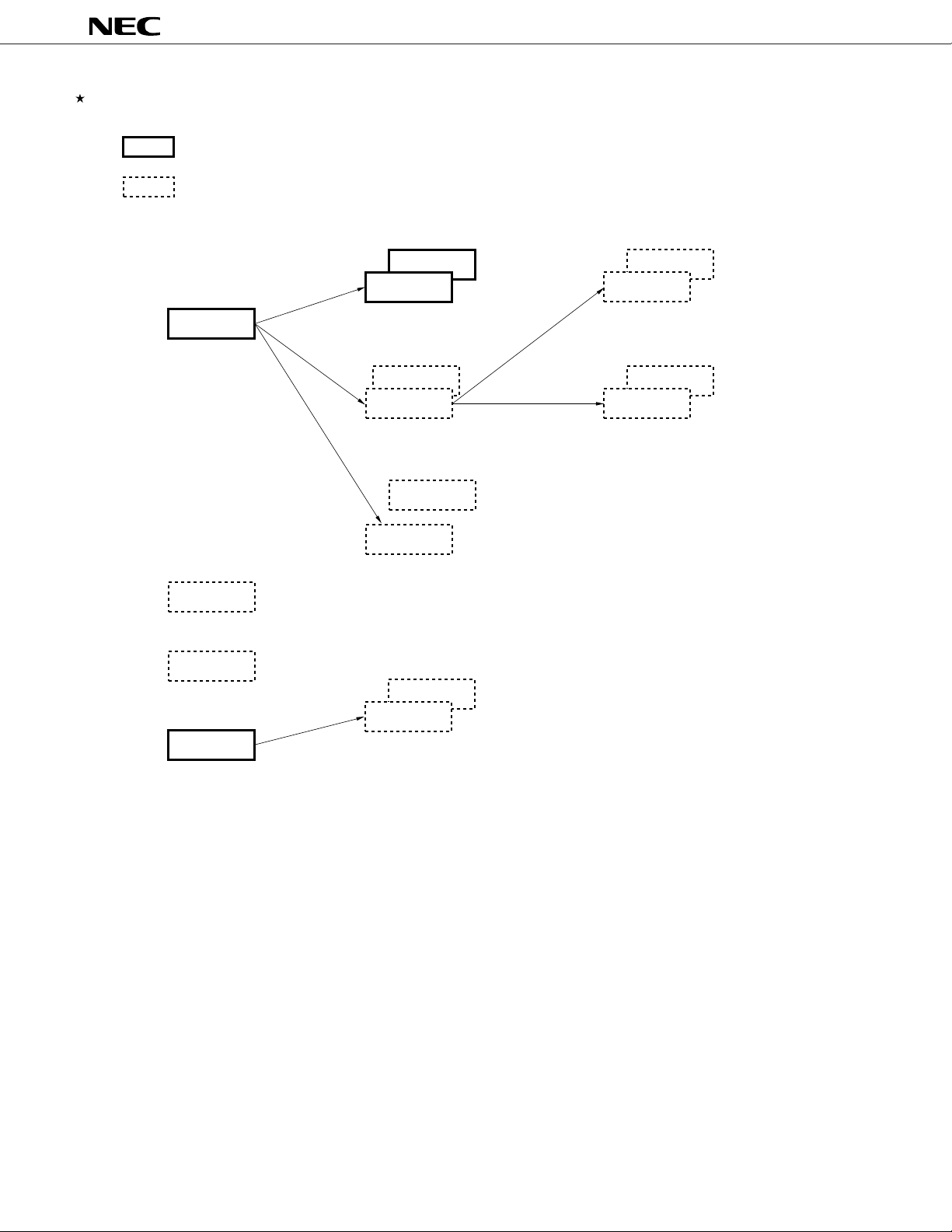
78K/IV SERIES PRODUCT DEVELOPMENT
: Under mass production
: Under development
µ
PD784031Y
Standard models
µPD784026
Enhanced A/D,
16-bit timer,
and power
management
ASSP models
µPD784908
Equipped with IEBus
controller
µPD78F4943
For CD-ROM,
56-Kbyte flash memory
µPD784915
Equipped with analog circuit for
software servo control VCR,
enhanced timer
TM
2
C bus supported
I
µPD784038Y
µPD784038
Enhanced internal memory capacity,
pin compatible with the µPD784026
µPD784216Y
µPD784216
100 pins,
enhanced I/O and
internal memory capacity
µPD784054
µPD784046
Equipped with 10-bit A/D
2
Multimaster I
µPD784928
Enhanced function of the µPD784915
C bus supported
µPD784928Y
2
Multimaster I
µPD784225
80 pins,
added ROM correction
Multimaster I
µPD784218
Enhanced internal memory capacity,
added ROM correction
C bus supported
µPD784225Y
2
C bus supportedMultimaster I2C bus supported
µPD784218Y
2
µ
PD784031Y
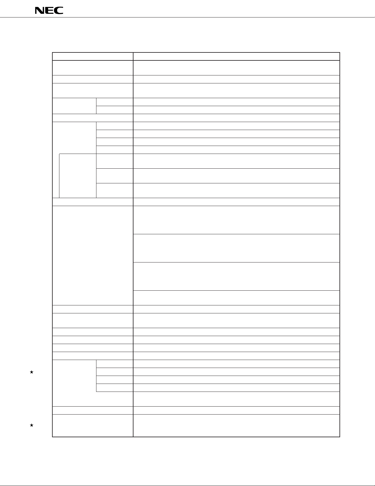
FUNCTIONS
Item Function
Number of basic instructions 113
(mnemonics)
General-purpose register 8 bits x 16 registers x 8 banks, or 16 bits x 8 registers x 8 banks (memory mapping)
Minimum instruction execution 125 ns/250 ns/500 ns/1000 ns (at 32 MHz)
time
Internal memory ROM None
RAM 2048 bytes
Memory space 1 Mbytes with program and data spaces combined
I/O port Total 46
Input 8
I/O 34
Output 4
Pins with
ancillary
Note
function
Real-time output port 4 bits x 2, or 8 bits x 1
Timer/counter Timer/counter 0: Timer register x 1 Pulse output
PWM output 12-bit resolution x 2 channels
Serial interface UART/IOE (3-wire serial I/O) : 2 channels (on-chip baud rate generator)
A/D converter 8-bit resolution x 8 channels
D/A converter 8-bit resolution x 2 channels
Watchdog timer 1 channel
Standby HALT/STOP/IDLE mode
Interrupt
Supply voltage VDD = 2.7 to 5.5 V
Package 80-pin plastic QFP (14 x 14 mm, thickness 2.7 mm)
Pins with pull- 32
up resistor
LEDs direct 8
drive output
Transistor 8
direct drive
Capture register x 1 • Toggle output
Compare register x 2 • PWM/PPG output
(16 bits) • One-shot pulse output
Timer/counter 1: Timer register x 1 Pulse output
Capture register x 1 • Real-time output (4 bits x 2)
(8/16 bits) Capture/compare register x 1
Compare register x 1
Timer/counter 2: Timer register x 1 Pulse output
Capture register x 1 • Toggle output
(8/16 bits) Capture/compare register x 1 • PWM/PPG output
Compare register x 1
Timer 3: Timer register x 1
(8/16 bits) Compare register x 1
CSI (3-wire serial I/O, 2-wire serial I/O, I2C bus) : 1 channel
Hardware source
Software source
Non-maskable
Maskable Internal: 16, external: 6
24 (internal: 17, external: 7 (variable sampling clock input: 1))
BRK instruction, BRKCS instruction, operand error
Internal: 1, external: 1
• 4 programmable priority levels
• 3 processing styles: vectored interrupt/macro service/context switching
80-pin plastic QFP (14 x 14 mm, thickness 1.4 mm)
80-pin plastic TQFP (fine pitch) (12 x 12 mm)
Note The pins with ancillary function are included in the I/O pins.
3

µ
PD784031Y
CONTENTS
1. DIFFERENCES AMONG MODELS IN µPD784038Y SUBSERIES.................................................. 6
2. MAJOR DIFFERENCES FROM µPD784026 SUBSERIES AND µPD78234 SUBSERIES.............. 7
3. PIN CONFIGURATION (Top View)................................................................................................... 8
4. BLOCK DIAGRAM ............................................................................................................................ 10
5. PIN FUNCTION ............................................................................................................................... 11
5.1 Port Pins ................................................................................................................................................ 11
5.2 Non-port Pins ........................................................................................................................................ 12
5.3 Types of Pin I/O Circuits and Connections for Unused Pins............................................................ 14
6. CPU ARCHITECTURE .................................................................................................................... 17
6.1 Memory Space....................................................................................................................................... 17
6.2 CPU Registers ....................................................................................................................................... 19
6.2.1 General-purpose registers .......................................................................................................... 19
6.2.2 Control registers.......................................................................................................................... 20
6.2.3 Special function registers (SFRs) ............................................................................................... 21
7. PERIPHERAL HARDWARE FUNCTIONS ..................................................................................... 26
7.1 Ports....................................................................................................................................................... 26
7.2 Clock Generation Circuit...................................................................................................................... 27
7.3 Real-time Output Port ........................................................................................................................... 29
7.4 Timer/Counter........................................................................................................................................ 30
7.5 PWM Output (PWM0, PWM1)................................................................................................................ 32
7.6 A/D Converter........................................................................................................................................ 33
7.7 D/A Converter........................................................................................................................................ 34
7.8 Serial Interface ...................................................................................................................................... 35
7.8.1 Asynchronous serial interface/3-wire serial I/O (UART/IOE) ...................................................... 36
7.8.2 Clocked serial interface (CSI) ..................................................................................................... 38
7.9 Edge Detection Function...................................................................................................................... 39
7.10 Watchdog Timer .................................................................................................................................... 40
8. INTERRUPT FUNCTION ................................................................................................................. 41
8.1 Interrupt Sources .................................................................................................................................. 41
8.2 Vectored Interrupt................................................................................................................................. 43
8.3 Context Switching................................................................................................................................. 44
8.4 Macro Service........................................................................................................................................ 44
8.5 Application Example of Macro Service............................................................................................... 45
4

µ
PD784031Y
9. LOCAL BUS INTERFACE .............................................................................................................. 47
9.1 Memory Expansion ............................................................................................................................... 47
9.2 Memory Space....................................................................................................................................... 48
9.3 Programmable Wait .............................................................................................................................. 49
9.4 Pseudo Static RAM Refresh Function................................................................................................. 49
9.5 Bus Hold Function ................................................................................................................................ 49
10. STANDBY FUNCTION .................................................................................................................... 50
11. RESET FUNCTION ......................................................................................................................... 51
12. INSTRUCTION SET ........................................................................................................................ 52
13. ELECTRICAL SPECIFICATIONS ................................................................................................... 57
14. PACKAGE DRAWINGS .................................................................................................................. 77
15. RECOMMENDED SOLDERING CONDITIONS .............................................................................. 80
APPENDIX A. DEVELOPMENT TOOLS ............................................................................................... 82
APPENDIX B. RELATED DOCUMENTS ............................................................................................... 84
5

µ
PD784031Y
1. DIFFERENCES AMONG MODELS IN µPD784038Y SUBSERIES
The only difference among the µPD784031Y, 784035Y, 784036Y, 784037Y, and 784038Y lies in the internal memory
capacity.
The µPD78P4038Y is provided with a 128-Kbyte one-time PROM or EPROM instead of the mask ROM of the
µ
PD784035Y, 784036Y, 784037Y, and 784038Y. These differences are summarized in Table 1-1.
Table 1-1. Differences among Models in µPD784038Y Subseries
Part NumberµPD784031Y
Item
Internal ROM None 48 Kbytes 64 Kbytes 96 Kbytes 128 Kbytes 128 Kbytes
Internal RAM 2048 bytes 3584 bytes 4352 bytes
Package 80-pin plastic QFP (14 x 14 mm, thickness 2.7 mm)
80-pin plastic QFP (14 x 14 mm, thickness 1.4 mm)
80-pin plastic TQFP (fine pitch) (12 x 12 mm)
µ
PD784035YµPD784036YµPD784037YµPD784038YµPD78P4038Y
(mask ROM) (mask ROM) (mask ROM) (mask ROM)
(one-time PROM
or EPROM)
80-pin ceramic
WQFN
(14 x 14 mm)
6

µ
PD784031Y
2. MAJOR DIFFERENCES FROM µPD784026 SUBSERIES AND µPD78234 SUBSERIES
Series Name
Item
Number of basic instructions 113 65
(mnemonics)
Minimum instruction execution time 125 ns 160 ns 333 ns
Memory space (program/data) 1 Mbytes combined 64 Kbytes/1 Mbytes
Timer/counter 16-bit timer/counter x 1 16-bit timer/counter x 1
Clock output function Provided None
Watchdog timer Provided None
Serial interface
Interrupt Context Provided None
switching
µ
PD784038Y Subseries
µ
PD784038 Subseries
(@ 32-MHz operation) (@ 25-MHz operation) (@ 12-MHz operation)
8-/16-bit timer/counter x 2 8-bit timer/counter x 2
8-/16-bit timer x 1 8-bit timer x 1
UART/IOE (3-wire serial
I/O) x 2 channels
CSI (3-wire serial I/O,
2-wire serial I/O, I2C
Note
bus
) x 1 channel
µ
PD784026 Subseries
UART/IOE (3-wire serial
I/O) x 2 channels
CSI (3-wire serial I/O, SBI)
x 1 channel
µ
PD78234 Subseries
UART x 1 channel
CSI (3-wire serial I/O, SBI)
x 1 channel
Priority 4 levels 2 levels
Standby function HALT/STOP/IDLE mode HALT/STOP mode
Operating clock Selectable from fXX/2, fXX/4, fXX/8, and fXX/16 Fixed to fXX/2
Pin function MODE pin None Specifies ROM-less mode
(always high level with
µ
PD78233 and 78237)
TEST pin Device test pin None
Usually, low level
Package
80-pin plastic QFP
(14 x 14 mm, thickness 2.7 mm)
80-pin plastic QFP
(14 x 14 mm, thickness 1.4 mm)
80-pin plastic TQFP
(fine pitch) (12 x 12 mm)
80-pin ceramic WQFN
(14 x 14 mm):
µ
PD78P4038Y and
78P4038 only
80-pin plastic QFP
(14 x 14 mm, thickness 2.7 mm)
80-pin plastic TQFP
(fine pitch) (12 x 12 mm):
µ
PD784021 only
80-pin ceramic WQFN
(14 x 14 mm):
µ
PD78P4026 only
80-pin plastic QFP
(14 x 14 mm, thickness 2.7 mm)
94-pin plastic QFP
(20 x 20 mm)
84-pin plastic QFJ
(1150 x 1150 mil)
94-pin ceramic WQFN
(20 x 20 mm):
µ
PD78P238 only
NoteµPD784038Y Subseries only
7
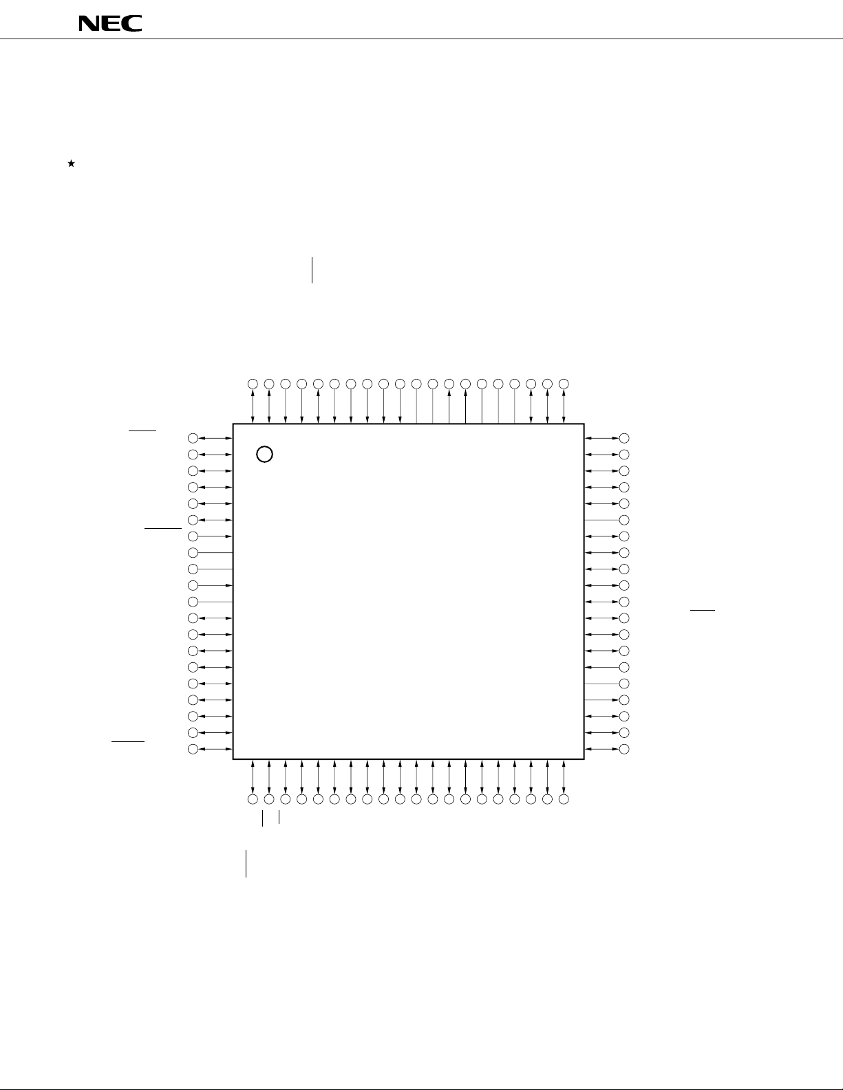
3. PIN CONFIGURATION (Top View)
• 80-pin plastic QFP (14 x 14 mm, thickness 2.7 mm)
µ
PD784031YGC-3B9
• 80-pin plastic QFP (14 x 14 mm, thickness 1.4 mm)
µ
PD784031YGC-8BT
• 80-pin plastic TQFP (fine pitch) (12 x 12 mm)
µ
PD784031YGK-BE9
µ
PD784031Y
P32/SCK0/SCL
P33/SO0/SDA
P34/TO0
P35/TO1
P36/TO2
P37/TO3
RESET
V
DD1
X2
X1
V
SS1
P00
P01
P02
P03
P04
P05
P06
P07
P67/REFRQ/HLDAK
REF3AVREF2
P31/TxD/SO1
P30/RxD/SI1
P27/SI0
P26/INTP5
P25/INTP4/ASCK/SCK1
P24/INTP3
P23/INTP2/CI
P22/INTP1
P21/INTP0
P20/NMI
AV
ANO1
80 6179 78 77 76 75 74 73 72 71 70 69 68 67 66 65 64 63 62
1
2
3
4
5
6
7
8
9
10
11
12
13
14
15
16
17
18
19
20
21 4022 23 24 25 26 27 28 29 30 31 32 33 34 35 36 37 38 39
ANO0
AVSSAV
REF1AVDD
P77/ANI7
P76/ANI6
P75/ANI5
60
59
58
57
56
55
54
53
52
51
50
49
48
47
46
45
44
43
42
41
P74/ANI4
P73/ANI3
P72/ANI2
P71/ANI1
P70/ANI0
V
DD0
P17
P16
P15
P14/TxD2/SO2
P13/TxD2/SI2
P12/ASCK2/SCK2
P11/PWM1
P10/PWM0
Note
TEST
V
SS0
ASTB
AD0
AD1
AD2
RD
WR
P66/WAIT/HLDRQ
Note Directly connect the TEST pin to V
8
P63/A19
P62/A18
SS0.
P61/A17
P60/A16
A15
A14
A13
A12
A11
A10
A9
A8
AD7
AD6
AD5
AD4
AD3

µ
PD784031Y
A8 to A19 : Address Bus
AD0 to AD7 : Address/Data Bus
ANI0 to ANI7 : Analog Input
ANO0, ANO1 : Analog Output
ASCK, ASCK2 : Asynchronous Serial Clock
ASTB : Address Strobe
DD : Analog Power Supply
AV
AVREF1 to AVREF3 : Reference Voltage
SS : Analog Ground
AV
CI : Clock Input
HLDAK : Hold Acknowledge
HLDRQ : Hold Request
INTP0 to INTP5 : Interrupt from Peripherals
NMI : Non-maskable Interrupt
P00 to P07 : Port0
P10 to P17 : Port1
P20 to P27 : Port2
P30 to P37 : Port3
P60 to P63, P66, P67
: Port6
P70 to P77 : Port7
PWM0, PWM1 : Pulse Width Modulation Output
RD : Read Strobe
REFRQ : Refresh Request
RESET : Reset
RxD, RxD2 : Receive Data
SCK0 to SCK2 : Serial Clock
SCL : Serial Clock
SDA : Serial Data
SI0 to SI2 : Serial Input
SO0 to SO2 : Serial Output
TEST : Test
TO0 to TO3 : Timer Output
TxD, TxD2 : Transmit Data
DD0, VDD1 : Power Supply
V
VSS0, VSS1 : Ground
WAIT : Wait
WR : Write Strobe
X1, X2 : Crystal
9
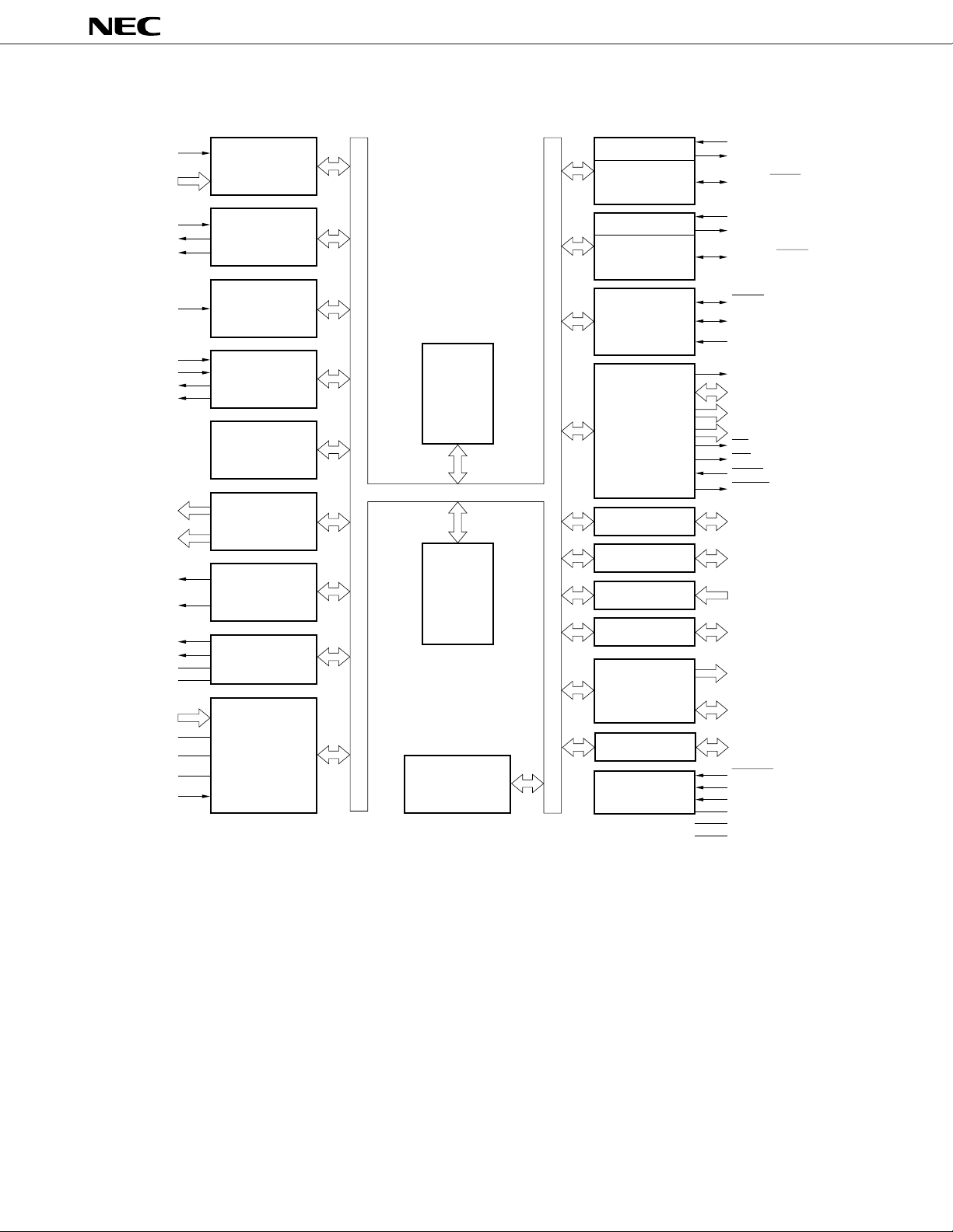
4. BLOCK DIAGRAM
µ
PD784031Y
NMI
INTP0 to INTP5
INTP3
TO0
TO1
INTP0
INTP1
INTP2/CI
TO2
TO3
P00
to
P03
P04
to
P07
PWM0
PWM1
ANO0
ANO1
REF2
AV
AV
REF3
ANI0 to ANI7
DD
AV
AV
REF1
AV
SS
INTP5
PROGRAMMABLE
INTERRUPT
CONTROLLER
TIMER/COUNTER0
(16 BITS)
TIMER/COUNTER1
(16 BITS)
TIMER/COUNTER2
(16 BITS)
TIMER3
(16 BITS)
REAL-TIME
OUTPUT PORT
PWM
D/A
CONVERTER
A/D
CONVERTER
78K/IV
CPU CORE
RAM
WATCHDOG
TIMER
UART/IOE2
BAUD-RATE
GENERATOR
UART/IOE1
BAUD-RATE
GENERATOR
CLOCKED
SERIAL
INTERFACE
BUS I/F
PORT0
PORT1
PORT2
PORT3
PORT6
PORT7
SYSTEM
CONTROL
RxD/SI1
TxD/SO1
ASCK/SCK1
RxD2/SI2
TxD2/SO2
ASCK2/SCK2
SCK0/SCL
SO0/SDA
SI0
ASTB
AD0
to
AD7
A8
to
A15
A16
to
A19
RD
WR
WAIT/HLDRQ
REFRQ/HLDAK
P00
to
P07
P10
to
P17
to
P27
P20
to
P37
P30
to
P63
P60
to
P67
P66
P70
to
P77
RESET
TEST
X1
X2
DD0,VDD1
V
V
SS0,VSS1
10

5. PIN FUNCTION
5.1 Port Pins
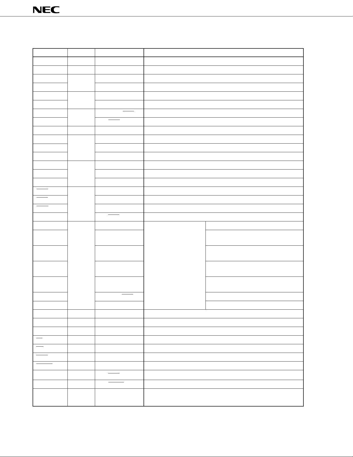
Pin Name I/O Alternate Function Function
µ
PD784031Y
P00 to P07 I/O –
P10 I/O PWM0
P11 PWM1
P12 ASCK2/SCK2
P13 RxD2/SI2
P14 TxD2/SO2
P15 to P17 –
P20 Input NMI
P21 INTP0
P22 INTP1
P23 INTP2/CI
P24 INTP3
P25 INTP4/ASCK/SCK1
P26 INTP5
P27 SI0
Port 0 (P0):
• 8-bit I/O port
• Can be used as real-time output port (4 bits x 2).
• Can be set in input or output mode bitwise.
• Pins set in input mode can be connected to internal pull-up
resistors by software.
• Can drive transistor.
Port 1 (P1):
• 8-bit I/O port
• Can be set in input or output mode bitwise.
• Pins set in input mode can be connected to internal pull-up
resistors by software.
• Can drive LEDs.
Port 2 (P2):
• 8-bit input port
• P20 cannot be used as general-purpose port pin (non-maskable
interrupt). However, its input level can be checked by interrupt
routine.
• P22 through P27 can be connected to internal pull-up resistors
by software in 6-bit units.
• P25/INTP4/ASCK/SCK1 pin can operate as SCK1 output pin if
so specified by CSIM1.
P30 I/O RxD/S1
P31 TxD/SO1
P32 SCK0/SCL
P33 SO0/SDA
P34 to P37 TO0 to TO3
P60 to P63 I/O A16 to A19
P66 WAIT/HLDRQ
P67 REFRQ/HLDAK
P70 to P77 I/O AN10 to AN17
Port 3 (P3):
• 8-bit I/O port
• Can be set in input or output mode bitwise.
• Pins set in input mode can be connected to internal pull-up
resistors by software.
Port 6 (P6):
• P60 through P63 is dedicated ports for output.
• P66 and P67 can be set in input or output mode bitwise.
• Pins set in input mode can be connected to internal pull-up
resistors by software.
Port 7 (P7):
• 8-bit I/O port
• Can be set in input or output mode bitwise.
11
µ
PD784031Y
5.2 Non-port Pins
Pin Name I/O Alternate Function Function
TO0 to TO3 Output P34 to P37 Timer output
CI Input P23/INTP2 Count clock input to timer/counter 2
RxD Input P30/SI1 Serial data input (UART0)
RxD2 P13/SI2 Serial data input (UART2)
TxD Output P31/SO1 Serial data output (UART0)
TxD2 P14/SO2 Serial data output (UART2)
ASCK Input P25/INTP4/SCK1 Baud rate clock input (UART0)
ASCK2 P12/SCK2 Baud rate clock input (UART2)
SDA I/O P33/SO0 Serial data input/output (2-wire serial I/O, I2C bus)
SI0 Input P27 Serial data input (3-wire serial I/O0)
SI1 P30/RxD Serial data input (3-wire serial I/O1)
SI2 P13/RxD2 Serial data input (3-wire serial I/O2)
SO0 Output P33/SDA Serial data output (3-wire serial I/O0)
SO1 P31/TxD Serial data output (3-wire serial I/O1)
SO2 P14/TxD2 Serial data output (3-wire serial I/O2)
SCK0 I/O P32/SCL Serial clock input/output (3-wire serial I/O0)
SCK1 P25/INTP4/ASCK Serial clock input/output (3-wire serial I/O1)
SCK2 P12/ASCK2 Serial clock input/output (3-wire serial I/O2)
SCL P32/SCK0 Serial clock input/output (2-wire serial I/O, I2C bus)
NMI Input P20 External interrupt requests –
INTP0 P21 • Count clock input to timer/counter 1
• Capture trigger signal of CR11 or CR12
INTP1 P22 • Count clock input to timer/counter 2
• Capture trigger signal of CR22
INTP2 P23/CI • Count clock input to timer/counter 2
• Capture trigger signal of CR21
INTP3 P24 • Count clock input to timer/counter 0
• Capture trigger signal of CR02
INTP4 P25/ASCK/SCK1 –
INTP5 P26 Conversion start trigger input to A/D converter
AD0 to AD7 I/O – Time-division address/data bus (for external memory connection)
A8 to A15 Output – Higher address bus (for external memory connection)
A16 to A19 Output P60 to P63 Higher address when address is extended (for external memory connection)
RD Output – Read strobe to external memory
WR Output – Write strobe to external memory
WAIT Input P66/HLDRQ Wait insertion
REFRQ Output P67/HLDAK Refresh pulse output to external pseudo static memory
HLDRQ Input P66/WAIT Bus hold request input
HLDAK Output P67/REFRQ Bus hold acknowledge output
ASTB Output – Latch timing output of time-division address (A0 through A7)
(when accessing external memory)
12

Pin Name I/O Alternate Function Function
RESET Input – Chip reset
X1 Input – Crystal connection for system clock oscillation
X2 – (Clock can also be input to X1.)
ANI0 to ANI7 Input P70 to P77 Analog voltage input to A/D converter
ANO0, ANO1 Output – Analog voltage output from D/A converter
AVREF1 – – Reference voltage to A/D converter
AVREF2, AVREF3
AVDD A/D converter power supply
AVSS A/D converter GND
Note 1
VDD0
Note 1
VDD1
Note 2
VSS0
Note 2
VSS1
TEST Directly connect to VSS0 (IC test pin).
Reference voltage to D/A converter
Power supply of port
Power supply except for port
GND of port
GND except for port
Notes 1. Provide the same potential to VDD0 and VDD1.
2. Provide the same potential to V
SS0 and VSS1.
µ
PD784031Y
13

5.3 Types of Pin I/O Circuits and Connections for Unused Pins
Table 5-1 shows types of pin I/O circuits and the connections for unused pins.
For the input/output circuit of each type, refer to Figure 5-1.
Table 5-1. Types of Pin I/O Circuits and Connections for Unused Pins (1/2)
Pin Name I/O Circuit Type I/O Recommended Connection for Unused Pins
P00 to P07 5-H I/O Input: Connect to VDD0.
P10/PWM0 Output: Open
P11/PWM1
P12/ASCK2/SCK2 8-C
P13/RxD2/SI2 5-H
P14/TxD2/SO2
P15 to P17
P20/NMI 2 Input Connect to VDD0 or VSS0.
P21/INTP0
P22/INTP1 2-C Connect to VDD0.
µ
PD784031Y
P23/INTP2/CI
P24/INTP3
P25/INTP4/ASCK/SCK1 8-C I/O Input: Connect to VDD0.
Output: Open
P26/INTP5 2-C Input Connect to VDD0.
P27/SI0
P30/RxD/SI1 5-H I/O Input: Connect to VDD0.
P31/TxD/SO1 Output: Open
P32/SCK0/SCL 10-B
P33/SO0/SDA
P34/TO0 to P37/TO3 5-H
AD0 to AD7
A8 to A15 Output
P60/A16 to P63/A19
RD
WR
P66/WAIT/HLDRQ I/O Input: Connect to VDD0.
P67/REFRQ/HLDAK Output: Open
P70/ANI0 to P77/ANI7 20-A Input: Connect to VDD0 or VSS0.
ANO0, ANO1 12 Output Open
Note
Open
Output: Open
ASTB 4-B
Note I/O circuit type of these pins is 5-H. However these pins perform only as output by an internal circuit.
14

Table 5-1. Types of Pin I/O Circuits and Connections for Unused Pins (2/2)
Pin Name I/O Circuit Type I/O Recommended Connection for Unused Pins
RESET 2 Input –
TEST 1-A Directly connect to VSS0.
AVREF1 to AVREF3 – Connect to VSS0.
AVSS
AVDD Connect to VDD0.
µ
PD784031Y
Caution Connect an I/O pin whose input/output mode is unstable to V
DD0 via a resistor of several 10 kΩ
(especially if the voltage on the reset input pin rises higher than the low-level input level on power
application or when the mode is switched between input and output by software).
Remark Because the circuit type numbers shown in the above table are commonly used with all the models in the 78K
Series, these numbers of some models are not serial (because some circuits are not provided to some models).
15
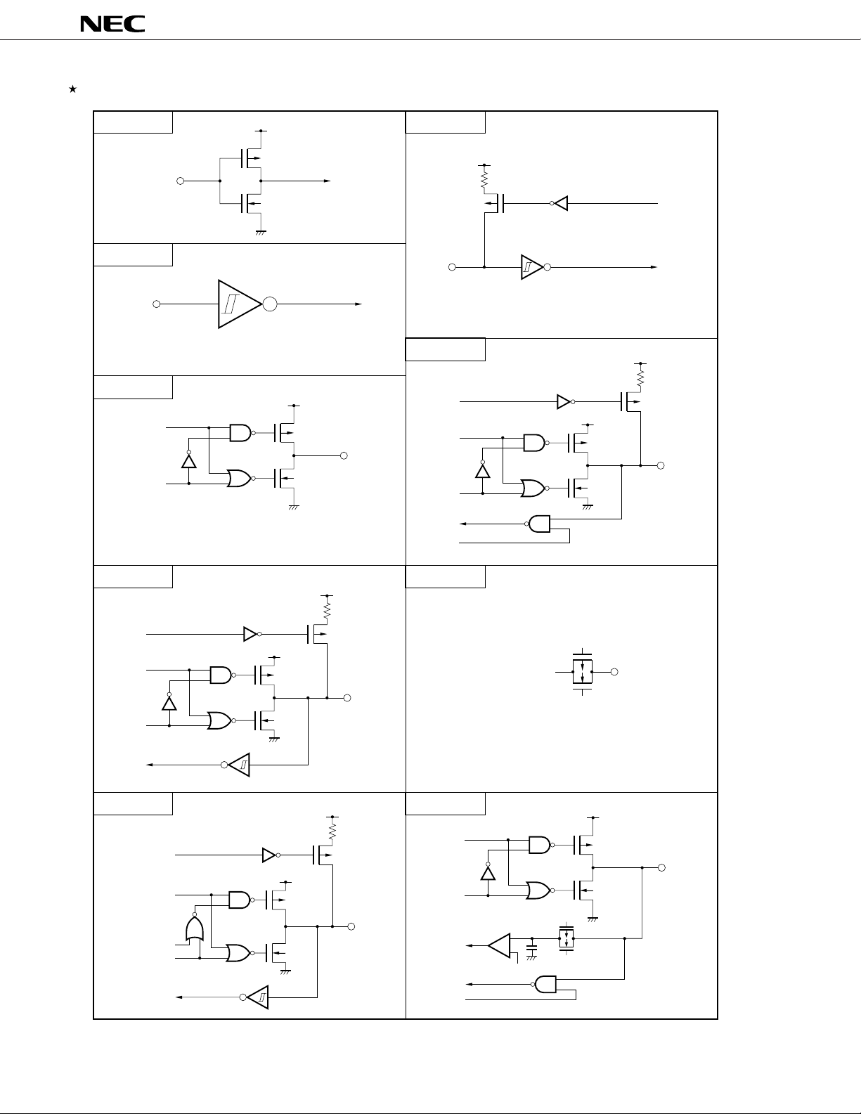
Figure 5-1. Types of Pin I/O Circuits
µ
PD784031Y
Type 1-A
DD0
V
P
IN
N
V
SS0
Type 2
IN
Schmitt trigger input with hysteresis characteristics
Type 4-B
data
output
disable
DD0
V
P
N
V
SS0
OUT
Type 2-C
V
DD0
P
IN
Schmitt trigger input with hysteresis characteristics
Type 5-H
pullup
enable
data
output
disable
DD0
V
P
N
V
SS0
pullup
enable
V
DD0
P
IN/OUT
Push-pull output that can go into a high-impedance
state (with both P-ch and N-ch off)
Type 8-C
pullup
enable
data
output
disable
DD0
V
P
N
V
SS0
Type 10-B
pullup
enable
DD0
V
data
open drain
output disable
P
N
V
SS0
input
enable
Type 12
V
DD0
P
P
Analog output voltage
IN/OUT
V
DD0
Type 20-A
N
data
P
OUT
DD0
V
P
IN/OUT
IN/OUT
output
disable
Comparator
+
–
AV
AV
REF
(threshold voltage)
N
V
SS0
P
N
SS
input
enable
16

µ
PD784031Y
6. CPU ARCHITECTURE
6.1 Memory Space
A memory space of 1 Mbytes can be accessed. Mapping of the internal data area (special function registers and internal
RAM) can be specified the LOCATION instruction. The LOCATION instruction must be always executed after reset
cancellation, and must not be used more than once.
(1) When LOCATION 0 instruction is executed
The internal data area is mapped in 0F700H to 0FFFFH.
(2) When LOCATION 0FH instruction is executed
The internal data area is mapped in FF700H to FFFFFH.
17

18
Figure 6-1. Memory Map of
µ
PD784031Y
On execution of
LOCATION 0 instruction
HFFFFF
External memory
(960 Kbytes)
H00001
HFFFF0
Special function registers (SFR)
HFDFF0
H0DFF0
H00FF0
HFFEF0
H00DF0
HFFCF0
(256 bytes)
Internal RAM
(2 Kbytes)
H007F0
HFF6F0
External memory
(63232 bytes)
H00000
Note
HFFEF0
General-purpose
registers (128 bytes)
H08EF0
HF7EF0
H13EF0
Macro service control word
area (44 bytes)
H60EF0
Data area (512 bytes)
H00DF0
HFFCF0
Program/data area
(1536 bytes)
H007F0
H00010
HFFF00
CALLF entry area
(2 Kbytes)
H00800
HFF700
H08000
HF7000
CALLT table area
(64 bytes)
H04000
HF3000
Vector table area
(64 bytes)
H00000
On execution of
LOCATION 0FH instruction
HFFFFF
Special function registers (SFR)
HFDFFF
H0DFFF
HFFEFF
H00FFF
HFFEFF
(256 bytes)
Internal RAM
(2 Kbytes)
H08EFF
HF7EFF
13
HEFF
H60EFF
H00DFF
HFFCFF
H007FF
HFF6FF
External memory
(1046272 bytes)
H007FF
HFFF00
H00800
HFF700
H08000
HF7000
H00001
HFFFF0
Note
H00000
µ
PD784031Y
Note Base area and entry area for reset or interrupt. However, the internal RAM area is not used as a reset entry area.
µ
(
PD784031Y
6.2 CPU Registers
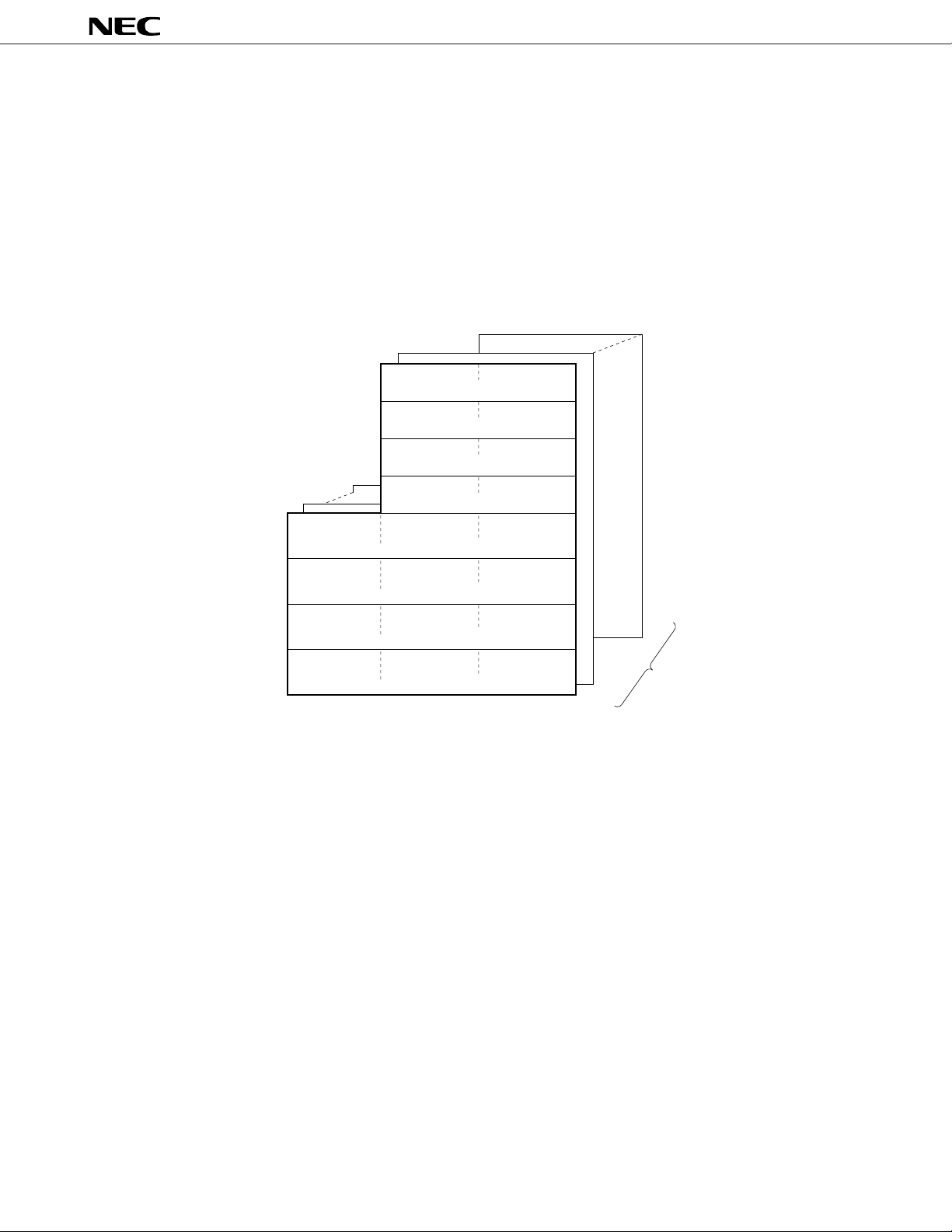
6.2.1 General-purpose registers
Sixteen 8-bit general-purpose registers are available. Two 8-bit registers can be also used in pairs as a 16-bit register.
Of the 16-bit registers, four can be used in combination with an 8-bit register for address expansion as 24-bit address
specification registers.
Eight banks of these registers are available which can be selected by using software or the context switching function.
The general-purpose registers except V, U, T, and W registers for address expansion are mapped to the internal RAM.
Figure 6-2. General-purpose Register Format
V
VVP (RG4)
U
UUP (RG5)
T
TDE (RG6)
W
WHL (RG7)
Parentheses
A (R1)
AX (RP0)
B (R3)
BC (RP1)
R5
R7
R9
VP (RP4)
R11
UP (RP5)
D (R13)
DE (RP6)
H (R15)
HL (RP7)
) indicate an absolute name.
X (R0)
C (R2)
R4
RP2
R6
RP3
R8
R10
E (R12)
L (R14)
8 banks
Caution Registers R4, R5, R6, R7, RP2, and RP3 can be used as X, A, C, B, AX, and BC registers, respectively,
by setting the RSS bit of the PSW to 1. However, use this function only for recycling the program of
the 78K/III Series.
19
6.2.2 Control registers
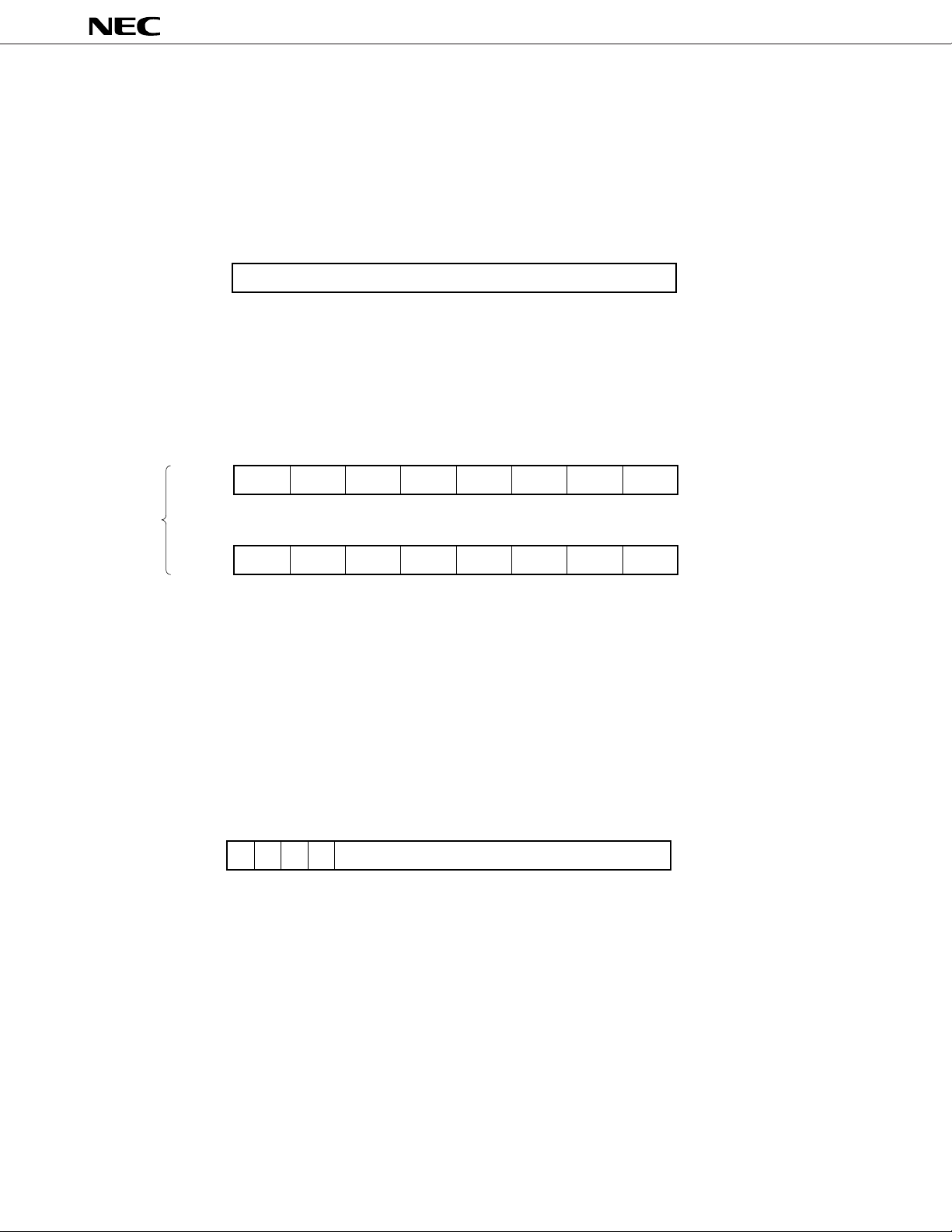
(1) Program counter (PC)
The program counter is a 20-bit register whose contents are automatically updated when the program is executed.
Figure 6-3. Program Counter (PC) Format
19 0
PC
(2) Program status word (PSW)
This register holds the statuses of the CPU. Its contents are automatically updated when the program is executed.
Figure 6-4. Program Status Word (PSW) Format
15 14 13 12 11 10 9 8
UF RBS2 RBS1 RBS0 – – – –PSWH
µ
PD784031Y
PSW
76543210
S Z RSS
Note
AC IE P/V 0 CYPSWL
Note This flag is provided to maintain compatibility with the 78K/III Series. Be sure to clear this flag to 0, except when
the software for the 78K/III Series is used.
(3) Stack pointer (SP)
This is a 24-bit pointer that holds the first address of the stack.
Be sure to write 0 to the higher 4 bits of this pointer.
Figure 6-5. Stack Pointer (SP) Format
23 0
SP
20
0000
20

µ
PD784031Y
6.2.3 Special function registers (SFRs)
The special function registers, such as the mode registers and control registers of the internal peripheral hardware, are
registers to which special functions are allocated. These registers are mapped to a 256-byte space of addresses 0FF00H
Note
through 0FFFFH
Note On execution of the LOCATION 0 instruction. FFF00H through FFFFFH on execution of the LOCATION 0FH
instruction.
Caution Do not access an address in this area to which no SFR is allocated. If such an address is accessed by
mistake, the
inputting the reset signal.
Table 6-1 lists the special function registers (SFRs). The meanings of the symbols in this table are as follows:
• Symbol................................ Symbol indicating an SFR. This symbol is reserved for NEC’s assembler (RA78K4).
.
µ
PD784031Y may be in the deadlock status. This deadlock status can be cleared only by
It can be used as an sfr variable by the #pragma sfr command with the C compiler
(CC78K4).
• R/W..................................... Indicates whether the SFR is read-only, write-only, or read/write.
R/W : Read/write
R : Read-only
W : Write-only
• Bit units for manipulation .... Bit units in which the value of the SFR can be manipulated.
SFRs that can be manipulated in 16-bit units can be described as the operand
sfrp of an instruction. To specify the address of this SFR, describe an even
address.
SFRs that can be manipulated in 1-bit units can be described as the operand of a
bit manipulation instruction.
• After reset........................... Indicates the status of the register when the RESET signal has been input.
21
µ
PD784031Y
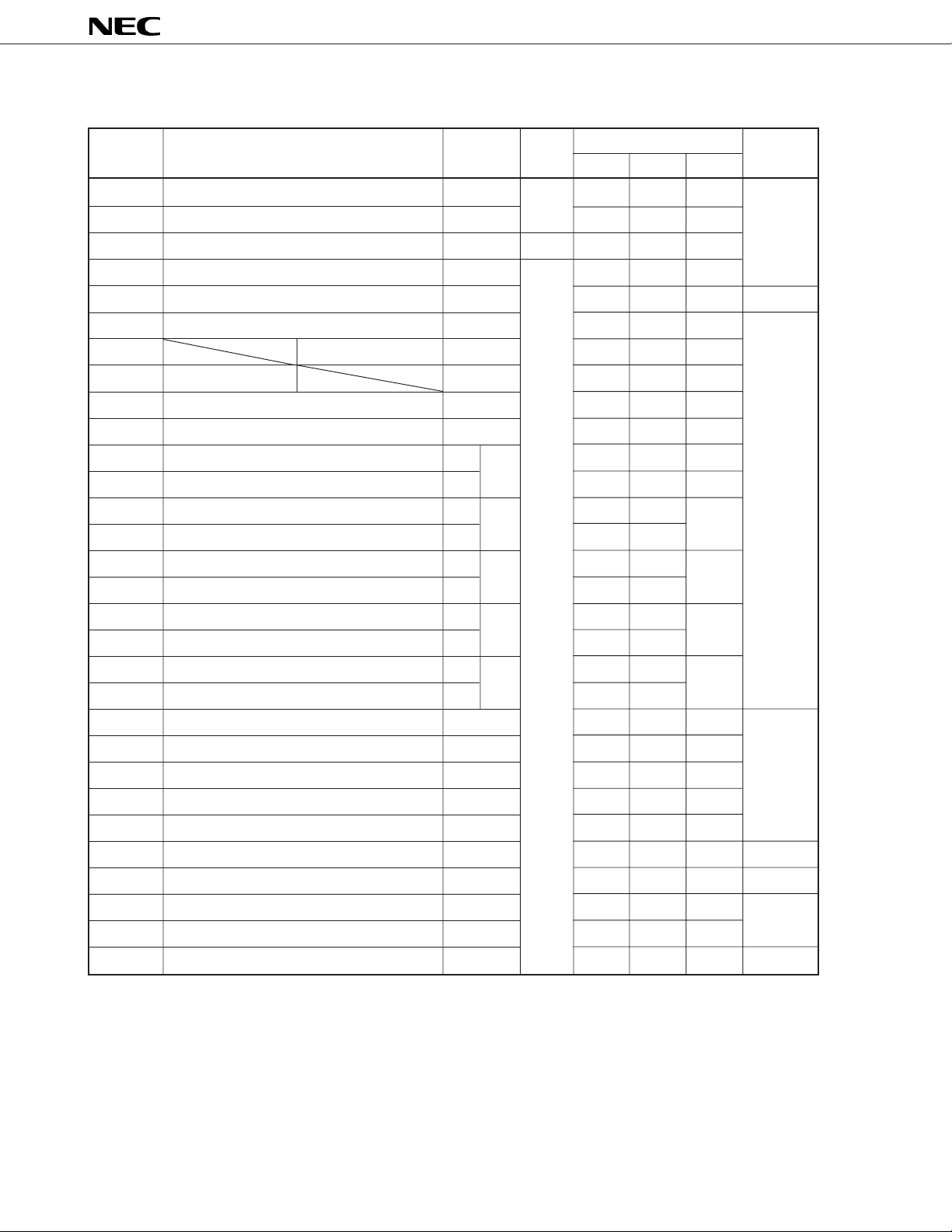
Table 6-1. Special Function Registers (SFRs) (1/4)
Note
Address
0FF00H Port 0 P0 R/W √√– Undefined
0FF01H Port 1 P1 √√–
0FF02H Port 2 P2 R √√–
0FF03H Port 3 P3 R/W √√–
0FF06H Port 6 P6 √√– 00H
0FF07H Port 7 P7 √√– Undefined
0FF0EH Port 0 buffer register L P0L √√–
Special Function Register (SFR) Name Symbol R/W Bit Units for Manipulation After Reset
1 bit 8 bits 16 bits
0FF0FH
0FF10H Compare register (timer/counter 0) CR00 – – √
0FF12H Capture/compare register (timer/counter 0) CR01 – – √
0FF14H Compare register L (timer/counter 1)
0FF15H Compare register H (timer/counter 1) – – –
0FF16H Capture/compare register L (timer/counter 1)
0FF17H Capture/compare register H (timer/counter 1) – – –
0FF18H Compare register L (timer/counter 2)
0FF19H Compare register H (timer/counter 2) – – –
0FF1AH Capture/compare register L (timer/counter 2)
0FF1BH Capture/compare register H (timer/counter 2) – – –
0FF1CH Compare register L (timer 3)
0FF1DH Compare register H (timer 3) – – –
0FF20H Port 0 mode register PM0 √√– FFH
0FF21H Port 1 mode register PM1 √√–
0FF23H Port 3 mode register PM3 √√–
0FF26H Port 6 mode register PM6 √√–
0FF27H Port 7 mode register PM7 √√–
Port 0 buffer register H
P0H √√–
CR10
CR11
CR20
CR21
CR30
CR10W
CR11W
CR20W
CR21W
CR30W
– √√
– √√
– √√
– √√
– √√
0FF2EH Real-time output port control register RTPC √√– 00H
0FF30H Capture/compare control register 0 CRC0 – √ – 10H
0FF31H Timer output control register TOC √√– 00H
0FF32H Capture/compare control register 1 CRC1 – √ –
0FF33H Capture/compare control register 2 CRC2 – √ – 10H
Note When the LOCATION 0 instruction is executed. When the LOCATION 0FH instruction is executed, “F0000H” is
added to this value.
22
µ
PD784031Y
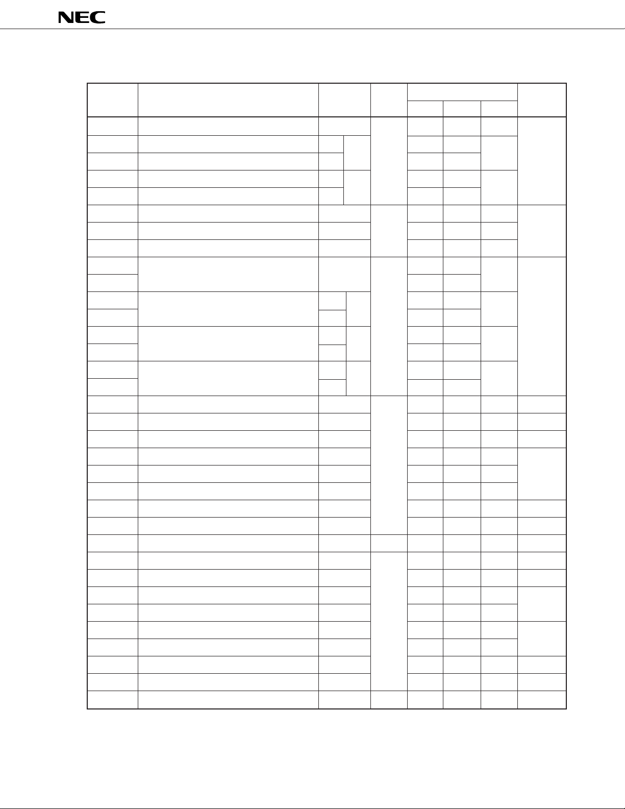
Table 6-1. Special Function Registers (SFRs) (2/4)
Note 1
Address
0FF36H Capture register (timer/counter 0) CR02 R – – √ 0000H
0FF38H Capture register L (timer/counter 1)
0FF39H Capture register H (timer/counter 1) – – –
Special Function Register (SFR) Name Symbol R/W Bit Units for Manipulation After Reset
1 bit 8 bits 16 bits
CR12
CR12W
– √√
0FF3AH Capture register L (timer/counter 2)
0FF3BH Capture register H (timer/counter 2) – – –
0FF41H Port 1 mode control register PMC1 R/W √√– 00H
0FF43H Port 3 mode control register PMC3 √√–
0FF4EH Pull-up resistor option register PUO √√–
0FF50H Timer register 0 TM0 R – – √ 0000H
0FF51H ––
0FF52H Timer register 1 TM1
0FF53H – – –
0FF54H Timer register 2 TM2
0FF55H – – –
0FF56H Timer register 3 TM3
0FF57H – – –
0FF5CH Prescaler mode register 0 PRM0 R/W – √ – 11H
0FF5DH Timer control register 0 TMC0 √√ – 00H
0FF5EH Prescaler mode register 1 PRM1 – √ – 11H
0FF5FH Timer control register 1 TMC1 √√– 00H
0FF60H D/A conversion value setting register 0 DACS0 – √ –
CR22
CR22W
TM1W
TM2W
TM3W
– √√
– √√
– √√
– √√
0FF61H D/A conversion value setting register 1 DACS1 – √ –
0FF62H D/A converter mode register DAM √√– 03H
0FF68H A/D converter mode register ADM √√– 00H
0FF6AH A/D conversion result register ADCR R – √ – Undefined
0FF70H PWM control register PWMC R/W √√– 05H
0FF71H PWM prescaler register PWPR – √ – 00H
0FF72H PWM modulo register 0 PWM0 – – √ Undefined
0FF74H PWM modulo register 1 PWM1 – – √
0FF7DH One-shot pulse output control register OSPC √√ – 00H
0FF80H I2C bus control register IICC √√–
0FF81H Prescaler mode register for serial clock SPRM – √ – 04H
0FF82H Clocked serial interface mode register CSIM √√– 00H
0FF83H Slave address register SVA
Note 2√Note 3
R/W
√ – 01H
Notes 1. When the LOCATION 0 instruction is executed. When the LOCATION 0FH instruction is executed, “F0000H”
is added to this value.
2. Bit 0 is read-only.
3. Only bit 0 can be manipulated in bit units.
23

µ
Table 6-1. Special Function Registers (SFRs) (3/4)
Note 1
Address
0FF84H Clocked serial interface mode register 1 CSIM1 R/W √√– 00H
0FF85H Clocked serial interface mode register 2 CSIM2 √√–
0FF86H Serial shift register SIO – √ –
0FF88H Asynchronous serial interface mode register ASIM √√–
0FF89H Asynchronous serial interface mode register 2 ASIM2 √√–
0FF8AH Asynchronous serial interface status register ASIS R √√–
Special Function Register (SFR) Name Symbol R/W Bit Units for Manipulation After Reset
1 bit 8 bits 16 bits
PD784031Y
0FF8BH
0FF8CH Serial receive buffer: UART0 RXB – √ – Undefined
0FF8DH Serial receive buffer: UART2 RXB2 R – √ –
0FF90H Baud rate generator control register BRGC – √ – 00H
0FF91H Baud rate generator control register 2 BRGC2 – √ –
0FFA0H External interrupt mode register 0 INTM0 √√–
0FFA1H External interrupt mode register 1 INTM1 √√–
0FFA4H Sampling clock select register SCS0 – √ –
0FFA8H In-service priority register ISPR R √√–
0FFAAH Interrupt mode control register IMC R/W √√– 80H
0FFACH Interrupt mask register 0L MK0L MK0 √√√FFFFH
0FFADH Interrupt mask register 0H
0FFAEH Interrupt mask register 1L MK1L √√– FFH
0FFC0H Standby control register STBC – √
0FFC2H Watchdog timer mode register WDM – √
Asynchronous serial interface status register 2
Serial transmit shift register: UART0 TXS W – √ –
Serial shift register: IOE1 SIO1 R/W – √ –
Serial transmit shift register: UART2 TXS2 W – √ –
Serial shift register: IOE2 SIO2 R/W – √ –
ASIS2 √√–
MK0H
√√
Note 2
Note 2
– 30H
– 00H
0FFC4H Memory expansion mode register MM √√– 20H
0FFC5H Hold mode register HLDM √√– 00H
0FFC6H Clock output mode register CLOM √√–
0FFC7H Programmable wait control register 1 PWC1 – √ – AAH
0FFC8H Programmable wait control register 2 PWC2 – – √ AAAAH
Notes 1. When the LOCATION 0 instruction is executed. When the LOCATION 0FH instruction is executed, “F0000H”
is added to this value.
2. Data can be written by using only dedicated instructions such as MOV STBC, #byte and MOV WDM, #byte,
and cannot be written with any other instructions.
24

µ
PD784031Y
Table 6-1. Special Function Registers (SFRs) (4/4)
Note
Address
0FFCCH Refresh mode register RFM R/W √√– 00H
0FFCDH Refresh area specification register RFA √√–
0FFCFH Oscillation stabilization time specification OSTS – √ –
0FFD0H to External SFR area – √√––
0FFDFH
0FFE0H Interrupt control register (INTP0) PIC0 √√– 43H
0FFE1H Interrupt control register (INTP1) PIC1 √√–
0FFE2H Interrupt control register (INTP2) PIC2 √√–
0FFE3H Interrupt control register (INTP3) PIC3 √√–
0FFE4H Interrupt control register (INTC00) CIC00 √√ –
0FFE5H Interrupt control register (INTC01) CIC01 √√ –
Special Function Register (SFR) Name Symbol R/W Bit Units for Manipulation After Reset
1 bit 8 bits 16 bits
register
0FFE6H Interrupt control register (INTC10) CIC10 √√ –
0FFE7H Interrupt control register (INTC11) CIC11 √√ –
0FFE8H Interrupt control register (INTC20) CIC20 √√ –
0FFE9H Interrupt control register (INTC21) CIC21 √√ –
0FFEAH Interrupt control register (INTC30) CIC30 √√ –
0FFEBH Interrupt control register (INTP4) PIC4 √√–
0FFECH Interrupt control register (INTP5) PIC5 √√–
0FFEDH Interrupt control register (INTAD) ADIC √√–
0FFEEH Interrupt control register (INTSER) SERIC √√–
0FFEFH Interrupt control register (INTSR) SRIC √√–
Interrupt control register (INTCSI1) CSIIC1 √√–
0FFF0H Interrupt control register (INTST) STIC √√–
0FFF1H Interrupt control register (INTCSI) CSIIC √√–
0FFF2H Interrupt control register (INTSER2) SERIC2 √√–
0FFF3H Interrupt control register (INTSR2) SRIC2 √√–
Interrupt control register (INTCSI2) CSIIC2 √√–
0FFF4H Interrupt control register (INTST2) STIC2 √√–
0FFF5H Interrupt control register (INTSPC) SPCIC √√–
Note When the LOCATION 0 instruction is executed. When the LOCATION 0FH instruction is executed, “F0000H” is
added to this value.
25
µ
PD784031Y
7. PERIPHERAL HARDWARE FUNCTIONS
7.1 Ports
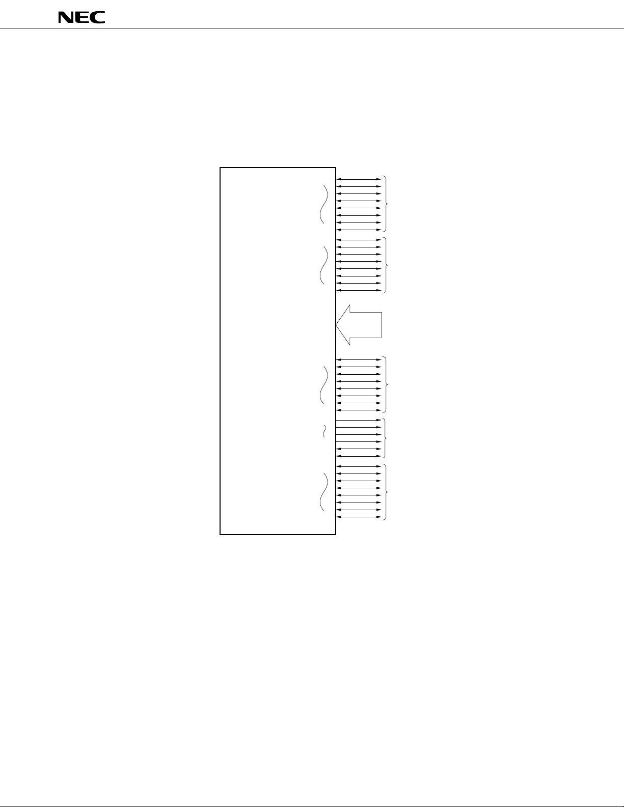
The ports shown in Figure 7-1 are provided to make various control operations possible. Table 7-1 shows the function
of each port. Ports 0 through 6 can be connected to internal pull-up resistors by software when inputting.
Figure 7-1. Port Configuration
P00
Port 0
P07
P10
Port 1
P17
P20 to P27
P30
P37
P60
P63
P66
P67
P70
P77
Port 2
8
Port 3
Port 6
Port 7
26
µ
PD784031Y
Table 7-1. Port Functions
Port Name Pin Name Function Specification of Pull-up Resistor
Connection by Software
Port 0 P00 to P07 • Can be set in input or output mode in 1-bit units. All port pins in input mode
• Can operate as 4-bit real-time output port
(P00 through P03 and P04 through P07).
• Can drive transistor.
Port 1 P10 to P17 • Can be set in input or output mode in 1-bit units. All port pins in input mode
• Can drive LEDs.
Port 2 P20 to P27 • Input port In 6-bit units (P22 through P27)
Port 3 P30 to P37 • Can be set in input or output mode in 1-bit units. All port pins in input mode
Port 6 P60 to P63 • Output only All port pins in input mode
P66, P67 • Can be set in input or output mode in 1-bit units.
Port 7 P70 to P77 • Can be set in input or output mode in 1-bit units. –
7.2 Clock Generation Circuit
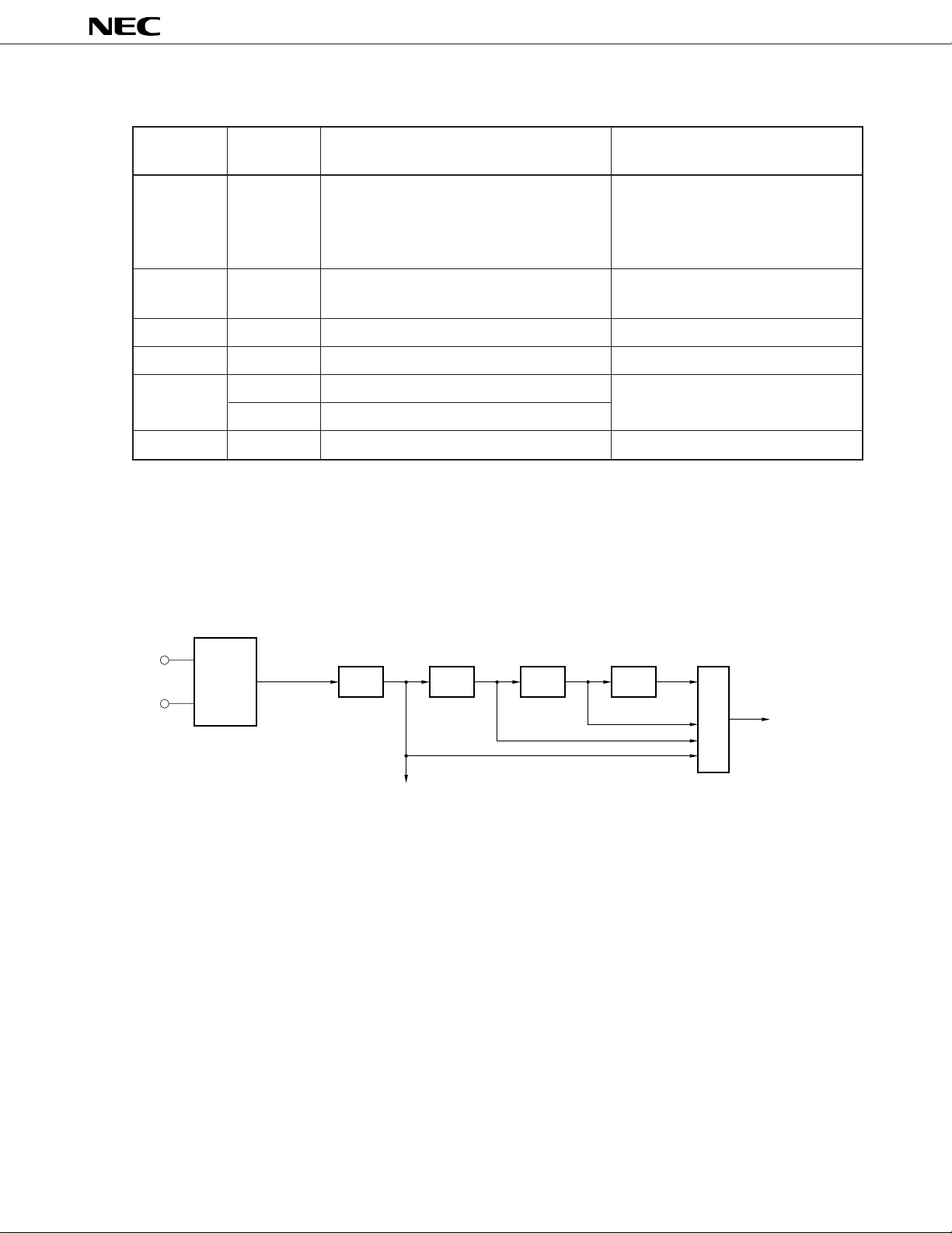
An on-chip clock generation circuit necessary for operation is provided. This clock generation circuit has a divider circuit.
If high-speed operation is not necessary, the internal operating frequency can be lowered by the divider circuit to reduce
the current consumption.
Figure 7-2. Block Diagram of Clock Generation Circuit
X1
Oscillation
circuit
X2
Remark fXX : oscillation frequency or external clock input
fCLK: internal operating frequency
f
XX
1/2 1/2 1/2 1/2
f
XX
/2
UART/IOE
INTP0 noise reduction circuit
Oscillation stabilization timer
Selector
CLK
f
CPU
Peripheral circuit
27
 Loading...