NEC UPD784021GK-BE9, UPD784021GC-3B9, UPD784020GC-3B9 Datasheet

DATA SHEET
MOS INTEGRATED CIRCUIT
mm
m
PD784020, 784021
mm
16/8-BIT SINGLE-CHIP MICROCOMPUTER
The mPD784021 is a product of the mPD784026 sub-series in the 78K/IV series. It contains various peripheral
hardware such as RAM, I/O ports, 8-bit resolution A/D and D/A converters, timers, serial interface, and interrupt
functions, as well as a high-speed, high-performance CPU.
m
PD784021 is a ROM-less product of the mPD784025 or mPD784026.
The
m
PD784020 differs from the mPD784021 only in its RAM size: 512 bytes are allocated for the mPD784020,
The
while 2048 bytes are allocated for the
For specific functions and other detailed information, consult the following user’s manual.
This manual is required reading for design work.
m
PD784026 Sub-Series User’s Manual, Hardware : U10898E
78K/IV Series User’s Manual, Instruction : U10905E
m
PD784021.
FEATURES
• 78K/IV series
• Pin-compatible with the
• Minimum instruction execution time: 160 ns
(at 25 MHz)
• Number of I/O ports: 46
• Timer/counters: 16-bit timer/counter ¥ 3 units
16-bit timer ¥ 1 unit
• Serial interface: 3 channels
UART/IOE (3-wire serial I/O) :2 channels
CSI (3-wire serial I/O, SBI) : 1 channel
APPLICATIONS
LBP, automatic-focusing camera, PPC, printer, electronic typewriter, air conditioner, electronic musical instruments, cellular telephone, etc.
m
PD78234 sub-series
• PWM outputs: 2
• Standby function
HALT/STOP/IDLE mode
• Clock frequency division function
• Watchdog timer : 1 channel
• A/D converter : 8-bit resolution ¥ 8 channels
• D/A converter : 8-bit resolution ¥ 2 channels
• Supply voltage : VDD = 2.7 to 5.5 V
This manual describes the
The information in this document is subject to change without notice.
Document No. U11514EJ1V0DS00 (1st edition)
(Previous No. IP-3234)
Date Published July 1996 P
Printed in Japan
mm
m
PD784021 unless otherwise specified.
mm
The mark H shows major revised points.
©
1990
1996

ORDERING INFORMATION
Part number Package Internal ROM Internal RAM
H
m
PD784020GC-3B9 80-pin plastic QFP (14 ¥ 14 mm) None 512
m
PD784021GC-3B9 80-pin plastic QFP (14 ¥ 14 mm) None 2048
H
m
PD784021GK-BE9 80-pin plastic TQFP (fine pitch) (12 ¥ 12 mm) None 2048
78K/IV SERIES PRODUCT DEVELOPMENT DIAGRAM
H
: Product under mass production
: Product under development
: Product under planning
Standard Products Development
PD784038Y sub-series
µ
Product containing for
2
C bus interface circuit
an I
PD784038 sub-series
µ
80-pin, 8-bit A/D, 8-bit D/A
ROM: 48K/64K/96K/128K
mm
m
PD784020, 784021
mm
(bytes) (bytes)
µ
PD784026 sub-series
80-pin, 8-bit A/D, 8-bit D/A
ROM: none/48K/64K
ASSP Development
PD784216 sub-series
µ
100-pin, 8-bit A/D, 8-bit D/A
ROM: 96K/128K
PD784915 sub-series
µ
VTR servo, 100-pin, built-in
analog amplifier
ROM: 48K/62K
µ
PD784216Y sub-series
Product containing for
2
two I
C bus interface circuits
PD784054
µ
80-pin, 10-bit A/D
ROM: 32K
µ
PD784046 sub-series sub-set
PD784046 sub-series
µ
80-pin, 10-bit A/D
ROM: 32K/64K
PD784908 sub-series
µ
100-pin, built-in IEBusTM
ROM: 96K/128K
PD784943 sub-series
µ
80-pin, for CD-ROM
ROM: 56K
2
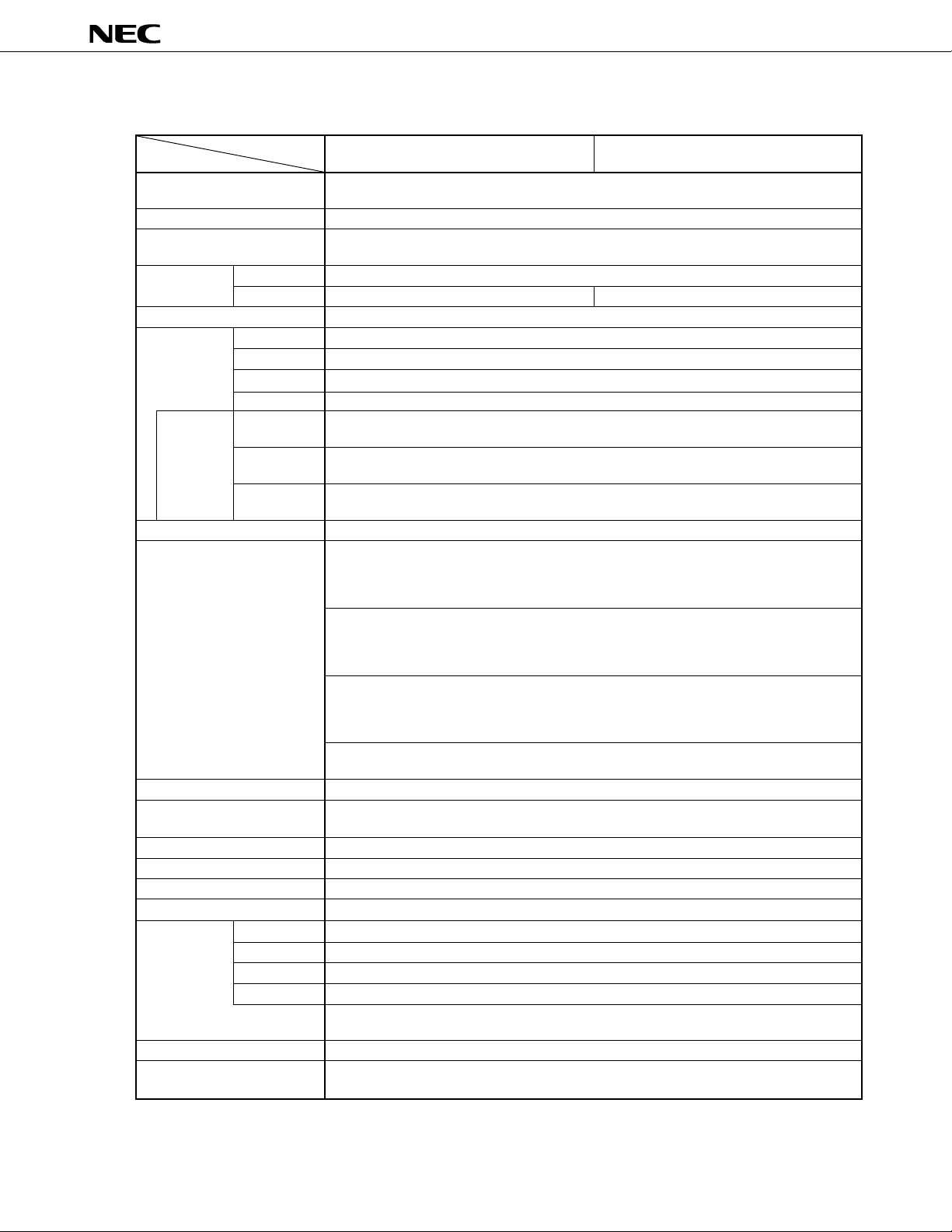
FUNCTIONS
mm
m
PD784020, 784021
mm
Product
Item
Number of basic instructions
(mnemonics)
General-purpose register
Minimum instruction execution
time
Internal
memory
Memory space
I/O ports
Additional
function
Note
pins
Real-time output ports
Timer/counter
PWM outputs
Serial interface
A/D converter
D/A converter
Watchdog timer
Standby
Interrupt Source
Supply voltage
Package
ROM
RAM
Total
Input
Input/output
Output
Pins with pull-
up resistor
LED direct
drive outputs
Transistor
direct drive
Software
Nonmaskable
Maskable
m
PD784020
113
8 bits ¥ 16 registers ¥ 8 banks, or 16 bits ¥ 8 registers ¥ 8 banks (memory mapping)
160 ns/320 ns/640 ns/1280 ns (at 25 MHz)
None
512 bytes 2048 bytes
Program and data: 1M byte
46
8
34
4
32
8
8
4 bits ¥ 2, or 8 bits ¥ 1
Timer/counter 0: Timer register ¥ 1 Pulse output capability
(16 bits) Capture register ¥ 1 Ý Toggle output
Compare register ¥ 2 Ý PWM/PPG output
Timer/counter 1: Timer register ¥ 1 Pulse output capability
(8/16 bits) Capture register ¥ 1 Ý Real-time output (4 bits ¥ 2)
Capture/compare register ¥ 1
Compare register ¥ 1
Timer/counter 2: Timer register ¥ 1 Pulse output capability
(8/16 bits) Capture register ¥ 1 Ý Toggle output
Capture/compare register ¥ 1 Ý PWM/PPG output
Compare register ¥ 1
Timer 3 : Timer register ¥ 1
(8/16 bits) Compare register ¥ 1
12-bit resolution ¥ 2 channels
UART/IOE (3-wire serial I/O) : 2 channels (incorporating baud rate generator)
CSI (3-wire serial I/O, SBI) : 1 channel
8-bit resolution ¥ 8 channels
8-bit resolution ¥ 2 channels
1 channel
HALT/STOP/IDLE mode
23 (16 internal, 7 external (sampling clock variable input: 1)) + BRK instruction
BRK instruction
1 internal, 1 external
15 internal, 6 external
Ý 4-level programmable priority
Ý 3 operation statuses: vectored interrupt, macro service, context switching
VDD = 2.7 to 5.5 V
80-pin plastic QFP (14 ¥ 14 mm)
80-pin plastic TQFP (fine pitch) (12 ¥ 12 mm): for the mPD784021 only
m
PD784021
Ý One-shot pulse output
H
H
Note Additional function pins are included in the I/O pins.
3

CONTENTS
mm
m
PD784020, 784021
mm
1. DIFFERENCES BETWEEN
2. MAIN DIFFERENCES BETWEEN
mm
m
PD784026 SUB-SERIES ........................................................... 6
mm
mm
m
PD784026 AND
mm
mm
m
PD78234 SUB-SERIES..................... 7
mm
3. PIN CONFIGURATION (TOP VIEW) ........................................................................................ 8
4. SYSTEM CONFIGURATION EXAMPLE (PPC) ....................................................................... 10
5. BLOCK DIAGRAM..................................................................................................................... 1 1
6. LIST OF PIN FUNCTIONS ........................................................................................................ 12
6.1 PORT PINS...................................................................................................................................... 12
6.2 NON-PORT PINS ............................................................................................................................ 13
6.3 I/O CIRCUITS FOR PINS AND HANDLING OF UNUSED PINS ................................................. 15
7. CPU ARCHITECTURE .............................................................................................................. 18
7.1 MEMORY SPACE ........................................................................................................................... 18
7.2 CPU REGISTERS............................................................................................................................ 21
7.2.1 General-Purpose Registers.......................................................................................... 21
7.2.2 Control Registers ........................................................................................................... 22
7.2.3 Special Function Registers (SFRs)............................................................................. 23
8. PERIPHERAL HARDWARE FUNCTIONS ............................................................................... 28
8.1 PORTS ............................................................................................................................................. 28
8.2 CLOCK GENERATOR .................................................................................................................... 29
8.3 REAL-TIME OUTPUT PORT .......................................................................................................... 31
8.4 TIMERS/COUNTERS ...................................................................................................................... 32
8.5 PWM OUTPUT (PWM0, PWM1)..................................................................................................... 34
8.6 A/D CONVERTER ........................................................................................................................... 35
8.7 D/A CONVERTER ........................................................................................................................... 36
8.8 SERIAL INTERFACE ...................................................................................................................... 37
8.8.1 Asynchronous Serial Interface/Three-Wire Serial I/O (UART/IOE) ......................... 38
8.8.2 Synchronous Serial Interface (CSI)............................................................................. 40
8.9 EDGE DETECTION FUNCTION..................................................................................................... 41
8.10 WATCHDOG TIMER ....................................................................................................................... 42
9. INTERRUPT FUNCTION ........................................................................................................... 43
9.1 INTERRUPT SOURCE.................................................................................................................... 43
9.2 VECTORED INTERRUPT ............................................................................................................... 45
9.3 CONTEXT SWITCHING .................................................................................................................. 4 6
9.4 MACRO SERVICE ........................................................................................................................... 46
9.5 EXAMPLES OF MACRO SERVICE APPLICATIONS .................................................................. 47
4

mm
m
PD784020, 784021
mm
10. LOCAL BUS INTERFACE......................................................................................................... 49
10.1 MEMORY EXPANSION .................................................................................................................. 49
10.2 MEMORY SPACE ........................................................................................................................... 50
10.3 PROGRAMMABLE WAIT............................................................................................................... 51
10.4 PSEUDO-STATIC RAM REFRESH FUNCTION ........................................................................... 51
10.5 BUS HOLD FUNCTION .................................................................................................................. 51
11. STANDBY FUNCTION .............................................................................................................. 5 2
12. RESET FUNCTION .................................................................................................................... 53
13. INSTRUCTION SET ................................................................................................................... 54
14. ELECTRICAL CHARACTERISTICS ......................................................................................... 59
15. PACKAGE DRAWINGS ............................................................................................................ 8 0
16. RECOMMENDED SOLDERING CONDITIONS ........................................................................ 82
APPENDIX A DEVELOPMENT TOOLS........................................................................................ 83
APPENDIX B RELATED DOCUMENTS ....................................................................................... 85
H
H
5
mm
m
PD784020, 784021
mm
1. DIFFERENCES BETWEEN
H
mm
m
PD784026 SUB-SERIES
mm
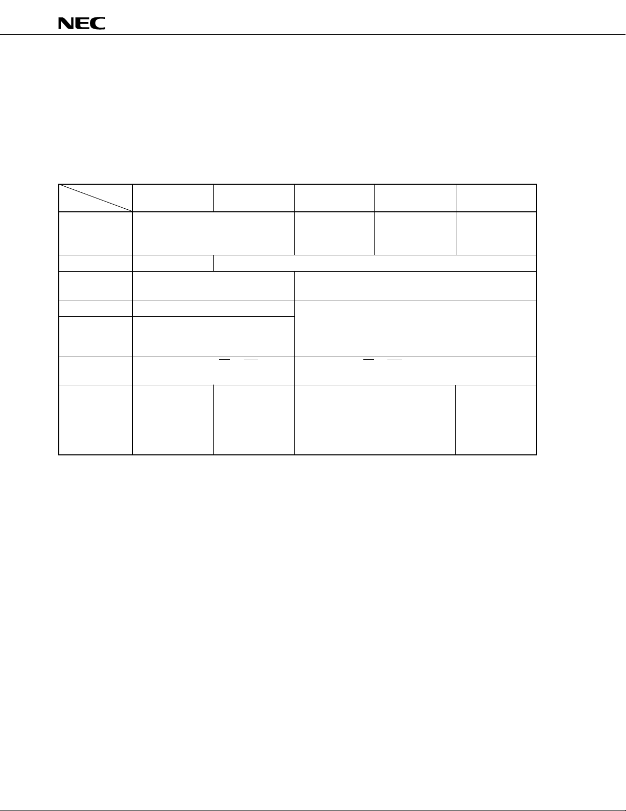
The only difference between the mPD784020, mPD784021, mPD784025, and mPD784026 is their capacity of
internal memory, port functions, and part of their packages.
The mPD78P4026 is produced by replacing the masked ROM in the mPD784025 or mPD784026 with 64K-byte one-
time PROM or EPROM. Table 1-1 shows the differences between these products.
mm
m
PD784026 Sub-Series
mm
m
PD784025
Product
Item
Internal ROM
Internal RAM
P40-P47
P50-P57
P60-P63
P64, P65
Package
Table 1-1 Differences between the
m
PD784020
None
512 bytes
Functions only as an address/data bus
Functions only as an address bus
Can be switched to an output-only port
or address bus in units of 2 bits, by
using software
Functions only as the RD or WR pin
80-pin plastic QFP
(14 ¥ 14 mm)
m
PD784021
2048 bytes
80-pin plastic QFP
(14 ¥ 14 mm)
80-pin plastic
TQFP (fine pitch)
(12 ¥ 12 mm)
48K bytes
(masked ROM)
Can be switched to a general-purpose port or address/data
bus, by using software
Can be switched to a general-purpose port or address bus in
units of 2 bits, by using software
Functions as the RD or WR pin when the local bus interface
is used. Functions as a general-purpose port in other cases.
80-pin plastic QFP (14 ¥ 14 mm)
m
PD784026
64K bytes
(masked ROM)
m
PD78P4026
64K bytes
(one-time PROM
or EPROM)
80-pin plastic QFP
(14 ¥ 14 mm)
80-pin ceramic
WQFN
(14 ¥ 14 mm)
6
mm
m
PD784020, 784021
mm
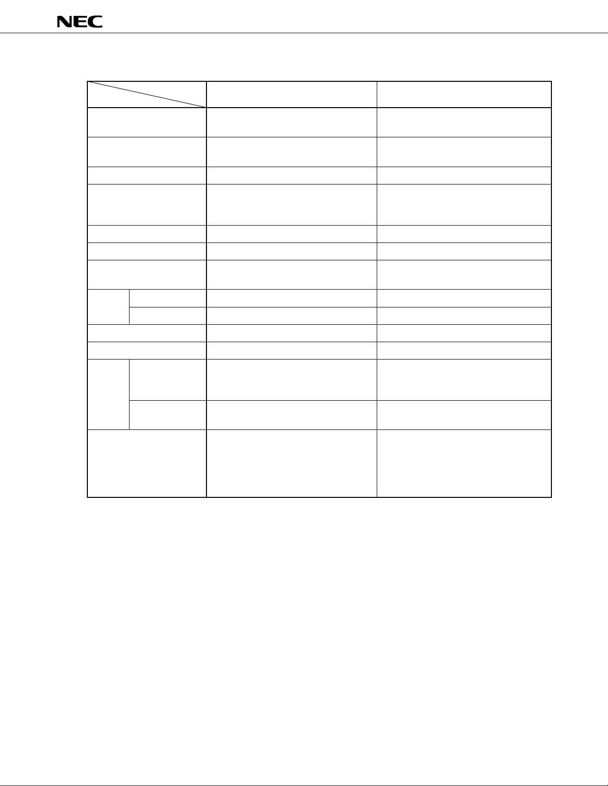
2. MAIN DIFFERENCES BETWEEN
Series
Item
Number of basic instructions 113 65
(mnemonics)
Minimum instruction execution 160 ns 333 ns
time (at 25 MHz) (at 12 MHz)
Memory space (program/data) 1M byte in total 64K bytes/1M byte
Timer/counter 16-bit timer/counter ¥ 1 16-bit timer/counter ¥ 1
8/16-bit timer/counter ¥ 2 8-bit timer/counter ¥ 2
8/16-bit timer ¥ 1 8-bit timer ¥ 1
Clock output function Available Unavailable
Watchdog timer Available Unavailable
Serial interface UART/IOE (3-wire serial I/O) ¥ 2 channels UART ¥ 1 channel
CSI (3-wire serial I/O, SBI) ¥ 1 channel CSI (3-wire serial I/O, SBI) ¥ 1 channel
Interrupt Context switching Available Unavailable
Priority 4 levels 2 levels
Standby function 3 modes
mm
m
PD784026 AND
mm
m
PD784026 sub-series
(HALT, STOP, IDLE)
mm
m
PD78234 SUB-SERIES
mm
m
PD78234 sub-series
2 modes (HALT, STOP)
Operation clock switching Selectable from fXX/2, fXX/4, fXX/8, or fXX/16 Fixed to fXX/2
Pin MODE pin Unavailable To specify ROM-less mode
functions (always in the high level for the mPD78233
or mPD78237)
TEST pin Pin for testing the device Unavailable
Low level during ordinary use
Package 80-pin plastic QFP (14 ¥ 14 mm) 80-pin plastic QFP (14 ¥ 14 mm)
80-pin plastic TQFP (fine pitch) 94-pin plastic QFP (20 ¥ 20 mm)
(12 ¥ 12 mm): for the mPD784021 only 84-pin plastic QFJ (1150 ¥ 1150 mil)
80-pin ceramic WQFN (14 ¥ 14 mm): 94-pin ceramic WQFN (20 ¥ 20 mm):
for the mPD78P4026 only for the mPD78P238 only
7
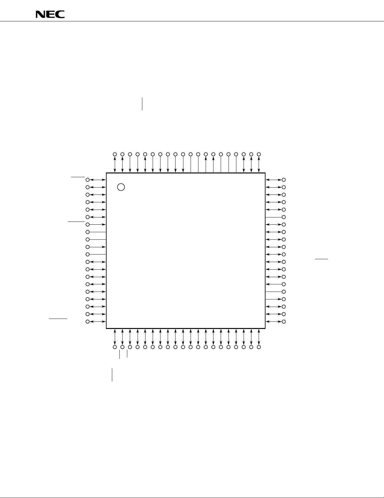
3. PIN CONFIGURATION (TOP VIEW)
• 80-pin plastic QFP (14 ¥ 14 mm)
H
m
PD784020GC-3B9, mPD784021GC-3B9
• 80-pin plastic TQFP (fine pitch) (12 ¥ 12 mm)
m
H
PD784021GK-BE9
P31/ TxD/SO1
P30/RxD/SI1
P27/SI0
P26/INTP5
P25/INTP4/ASCK/SCK1
P24/INTP3
P23/INTP2/CI
P22/INTP1
REF3
P21/INTP0
P20/NMI
AV
REF2
AV
ANO1
ANO0
SS
AV
REF1
AV
DD
P77/ANI7
AV
mm
m
PD784020, 784021
mm
P76/ANI6
P75/ANI5
P32/SCK0
P33/SO0/SB0
P34/ TO0
P35/TO1
P36/TO2
P37/TO3
RESET
V
X2
X1
V
P00
P01
P02
P03
P04
P05
P06
P07
P67/REFRQ/HLDAK
80 79 78 77 76 75 74 73 72 71 70 69 68 67 66 65 64 63 62 61
1
2
3
4
5
6
7
DD
SS
8
9
10
11
12
13
14
15
16
17
18
19
20
21 22 23 24 25 26 27 28 29 30 31 32 33 34 35 36 37 38 39 40
A9
WR
RD
P63/A19
P62/A18
P61/A17
P60/A16
A15
A14
A13
A12
A11
A10
A8
AD7
AD6
AD5
AD4
60
59
58
57
56
55
54
53
52
51
50
49
48
47
46
45
44
43
42
41
AD3
P74/ANI4
P73/ANI3
P72/ANI2
P71/ANI1
P70/ANI0
DD
V
P17
P16
P15
P14/T
X
D2/SO2
X
D2/SI2
P13/R
P12/ASCK2/SCK2
P11/PWM1
P10/PWM0
Note
TEST
V
ASTB
AD0
AD1
AD2
SS
P66/ WAIT/HLDRQ
Note Connect the TEST pin to VSS directly.
8

mm
m
PD784020, 784021
mm
P00-P07 : Port 0 A8-A19 : Address bus
P10-P17 : Port 1 RD : Read strobe
P20-P27 : Port 2 WR : Write strobe
P30-P37 : Port 3 WAIT : Wait
P60-P63, P66, P67 : Port 6 HLDRQ : Hold request
P70-P77 : Port 7 HLDAK : Hold acknowledge
TO0-TO3 : Timer output ASTB : Address strobe
CI : Clock input REFRQ : Refresh request
RxD, RxD2 : Receive data RESET : Reset
TxD, TxD2 : Transmit data X1, X2 : Crystal
SCK0-SCK2 : Serial clock ANI0-ANI7 : Analog input
ASCK, ASCK2 : Asynchronous serial clock ANO0, ANO1 : Analog output
SI0-SI2 : Serial input AV
SO0-SO2 : Serial output AV
SB0 : Serial bus AV
PWM0, PWM1 : Pulse width modulation output V
NMI : Non-maskable interrupt V
INTP0-INTP5 : Interrupt from peripherals TEST : Test
AD0-AD7 : Address/data bus
REF1-AVREF3 : Reference voltage
DD : Analog power supply
SS : Analog ground
DD : Power supply
SS : Ground
9
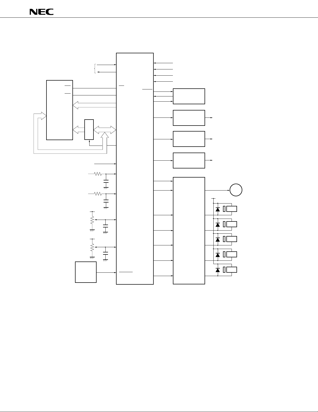
4. SYSTEM CONFIGURATION EXAMPLE (PPC)
µ
PD784021
mm
m
PD784020, 784021
mm
Serial
communication
µ
PD27C1001A
O0-O7
A0-A7
Sensing paper transport
Temperature of the
fusing heater
Brightness of the lamp
Lever for adjusting
the tone of the copy
Lever for compensating
the tone of the copy
µ
PD74HC573
Reset
circuit
Latch
RxD
TxD
RDOE
A17CE
A8-A16A8-A16
AD0-AD7
ASTB
INTP0
ANI0
ANI1
ANI2
ANI3
RESET
P11
P15
P16
P17
SCK1
SI1
SO1
P04
P06
P07
P66
PWM0
P00-P03
P33
P34
P35
P36
P37
Sensing paper
Sensing paper feed
Sensing paper ejection
Sensing the position of the scanner station
Operator
panel
High-voltage
control circuit
Fusing heater
control circuit
Lamp regulator
Driver
Drum, toner, and charge for
transfer
Fusing roller
Lamp for lighting the original
Lamp for discharging
(DC stepping motor)
Solenoid
Main motor
M
Clutch for stopping
SL
the scanner station
Clutch for forwarding
SL
the scanner station
Clutch for the resist
SL
shutter
Clutch for manual
SL
feeding
Clutch for cassette
SL
feeding
10

5. BLOCK DIAGRAM
mm
m
PD784020, 784021
mm
NMI
INTP0-INTP5
INTP3
TO0
TO1
INTP0
INTP1
INTP2/CI
TO2
TO3
P00-P03
P04-P07
PWM0
PWM1
Programmable
interrupt controller
Timer/counter 0
(16 bits)
Timer/counter 1
(16 bits)
Timer/counter 2
(16 bits)
Timer 3
(16 bits)
Real-time output
port
PWM
78K/IV
CPU core
RAM
UART/IOE2
Baud-rate
generator
UART/IOE1
Baud-rate
generator
Clocked serial
interface
Bus interface
Port 0
Port 1
Port 2
RxD/SI1
TxD/SO1
ASCK/SCK1
RxD2/SI2
TxD2/SO2
ASCK2/SCK2
SCK0
SO0/SB0
SI0
ASTB
AD0-AD7
A8-A15
A16-A19
RD
WR
WAIT/HLDRQ
REFRQ/HLDAK
P00-P07
P10-P17
P20-P27
ANO0
ANO1
AV
REF2
AV
REF3
ANI0-ANI7
AV
DD
AV
REF1
AV
INTP5
SS
D/A converter
A/D converter
Watchdog timer
Remark The internal ROM or RAM capacity differs for each product.
Port 3
Port 6
Port 7
System control
P30-P37
P60-P63
P60, P67
P70-P77
RESET
TEST
X1
X2
V
DD
V
SS
11
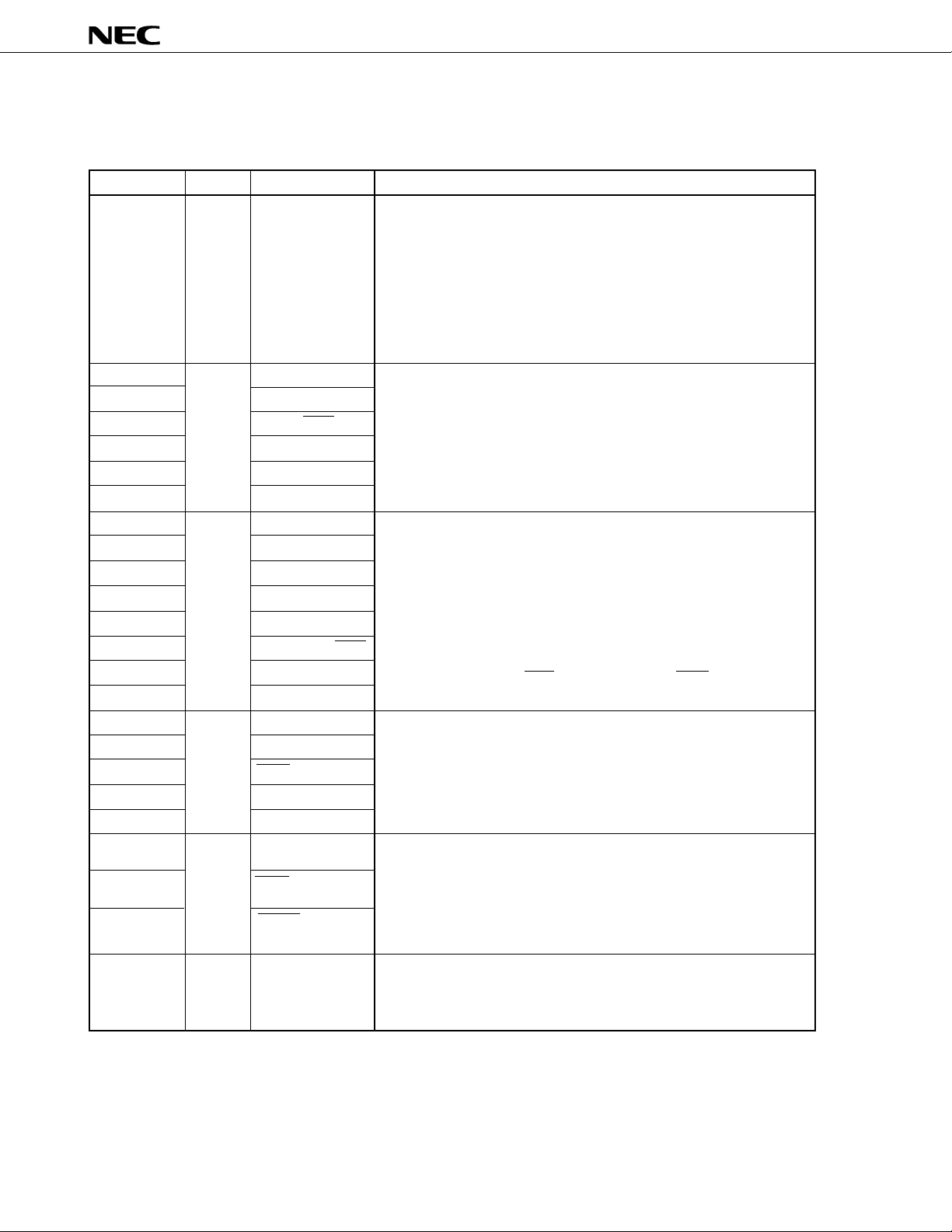
6. LIST OF PIN FUNCTIONS
6.1 PORT PINS
mm
m
PD784020, 784021
mm
Pin
P00-P07
P10
P11
P12
P13
P14
P15-P17
P20
P21
P22
P23
P24
P25
P26
P27
P30
P31
P32
P33
P34-P37
P60-P63
P66
P67
P70-P77
I/O
I/O
I/O
Input
I/O
I/O
I/O
Dual-function
—
PWM0
PWM1
ASCK2/SCK2
RxD2/SI2
TxD2/SO2
—
NMI
INTP0
INTP1
INTP2/CI
INTP3
INTP4/ASCK/SCK1
INTP5
SI0
RxD/SI1
TxD/SO1
SCK0
SO0/SB0
TO0-TO3
A16-A19
WAIT/HLDRQ
REFRQ/HLDAK
ANI0-ANI7
Function
Port 0 (P0):
Ý 8-bit I/O port
Ý Functions as a real-time output port (4 bits ¥ 2).
Ý Inputs and outputs can be specified bit by bit.
Ý The use of the pull-up resistors can be specified by software for the pins
in the input mode together.
Ý Can drive a transistor.
Port 1 (P1):
Ý 8-bit I/O port
Ý Inputs and outputs can be specified bit by bit.
Ý The use of the pull-up resistors can be specified by software for the pins
in the input mode together.
Ý Can drive LED.
Port 2 (P2):
Ý 8-bit input-only port
Ý P20 does not function as a general-purpose port (nonmaskable inter-
rupt). However, the input level can be checked by an interrupt service
routine.
Ý The use of the pull-up resistors can be specified by software for pins
P22 to P27 (in units of 6 bits).
Ý The P25/INTP4/ASCK/SCK1 pin functions as the SCK1 output pin by
CSIM1.
Port 3 (P3):
Ý 8-bit I/O port
Ý Inputs and outputs can be specified bit by bit.
Ý The use of the pull-up resistors can be specified by software for the pins
in the input mode together.
Port 6 (P6):
Ý P60 to P63 are an output-only port.
Ý Inputs and outputs can be specified bit by bit for pins P66 and P67.
Ý The use of the pull-up resistors can be specified by software for the pins
in the input mode together.
Port 7 (P7):
Ý 8-bit I/O port
Ý Inputs and outputs can be specified bit by bit.
12
mm
m
PD784020, 784021
mm
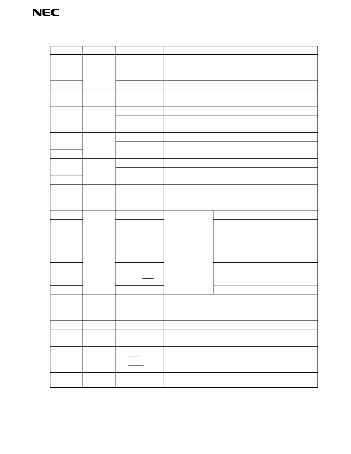
6.2 NON-PORT PINS (1/2)
Pin I/O Dual-function Function
TO0-TO3 Output P34-P37 Timer output
CI Input P23/INTP2 Input of a count clock for timer/counter 2
RXD Input P30/SI1 Serial data input (UART0)
RXD2 P13/SI2 Serial data input (UART2)
TXD Output P31/SO1 Serial data output (UART0)
TXD2 P14/SO2 Serial data output (UART2)
ASCK Input P25/INTP4/SCK1 Baud rate clock input (UART0)
ASCK2 P12/SCK2 Baud rate clock input (UART2)
SB0 I/O P33/SO0 Serial data I/O (SBI)
SI0 Input P27 Serial data input (3-wire serial I/O0)
SI1 P30/RXD Serial data input (3-wire serial I/O1)
SI2 P13/RXD2 Serial data input (3-wire serial I/O2)
SO0 Output P33/SB0 Serial data output (3-wire serial I/O0)
SO1 P31/TXD Serial data output (3-wire serial I/O1)
SO2 P14/TXD2 Serial data output (3-wire serial I/O2)
SCK0 I/O P32 Serial clock I/O (3-wire serial I/O0, SBI)
SCK1 P25/INTP4/ASCK Serial clock I/O (3-wire serial I/O1)
SCK2 P12/ASCK2 Serial clock I/O (3-wire serial I/O2)
NMI Input P20
INTP0 P21 Ý Input of a count clock for timer/counter 1
INTP1 P22 Ý Input of a count clock for timer/counter 2
INTP2 P23/CI Ý Input of a count clock for timer/counter 2
INTP3 P24 Ý Input of a count clock for timer/counter 0
INTP4 P25/ASCK/SCK1 —
INTP5 P26
AD0-AD7 I/O — Time multiplexing address/data bus (for connecting external memory)
A8-A15 Output — High-order address bus (for connecting external memory)
A16-A19 Output P60-P63
RD Output — Strobe signal output for reading the contents of external memory
WR Output — Strobe signal output for writing on external memory
WAIT Input P66/HLDRQ Wait signal insertion
REFRQ Output P67/HLDAK Refresh pulse output to external pseudo static memory
HLDRQ Input P66/WAIT Input of bus hold request
HLDAK Output P67/REFRQ Output of bus hold response
ASTB Output — Latch timing output of time multiplexing address (A0-A7) (for
External interrupt request
Ý Capture/trigger signal for CR11 or CR12
Ý Capture/trigger signal for CR22
Ý Capture/trigger signal for CR21
Ý Capture/trigger signal for CR02
Input of a conversion start trigger for A/D converter
High-order address bus during address expansion (for connecting external memory)
connecting external memory)
—
13
mm
m
PD784020, 784021
mm
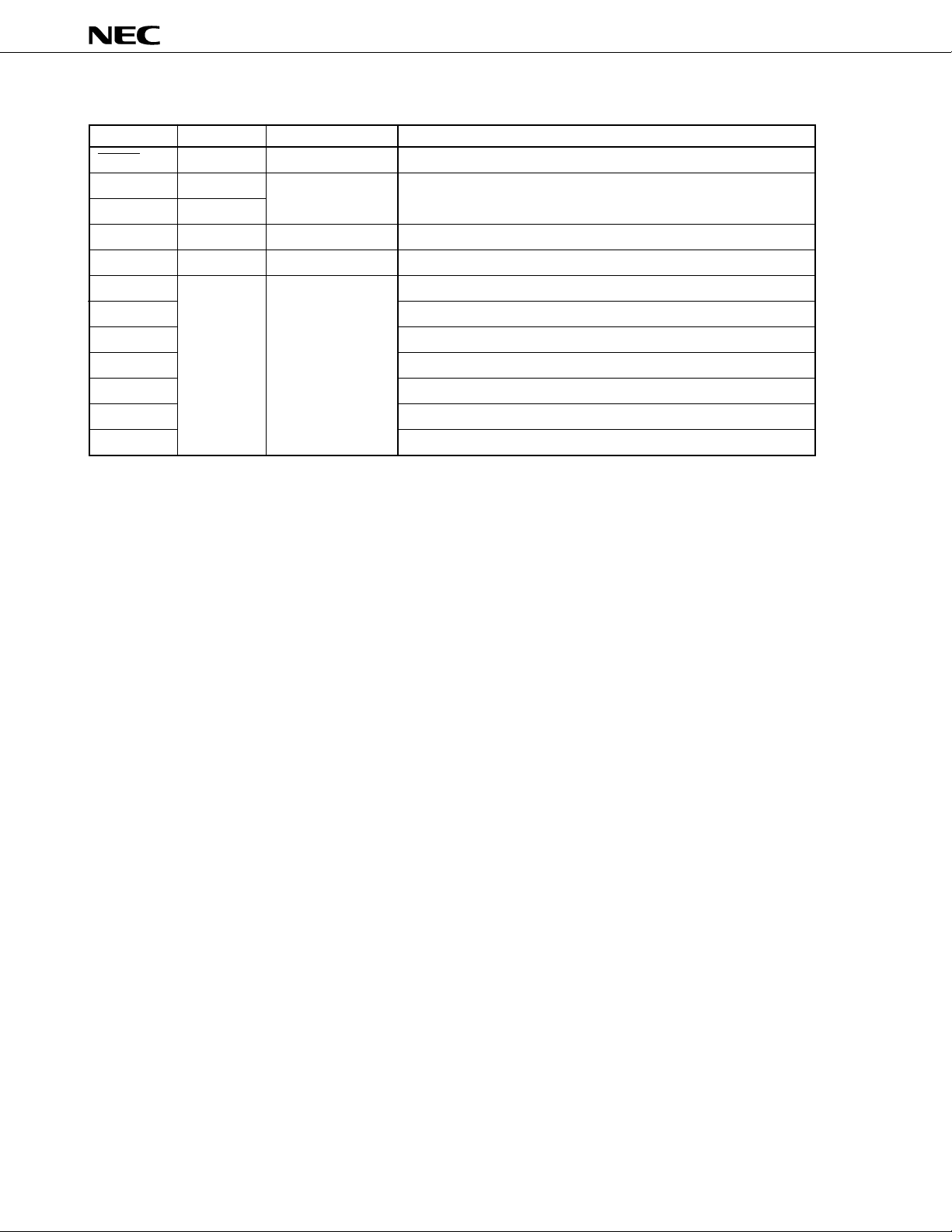
6.2 NON-PORT PINS (2/2)
Pin I/O Dual-function Function
RESET Input — Chip reset
X1 Input — Crystal input for system clock oscillation (A clock pulse can also be
X2 —
ANI0-ANI7 Input P70-P77 Analog voltage inputs for the A/D converter
ANO0, ANO1 Output — Analog voltage inputs for the D/A converter
AVREF1 — — Application of A/D converter reference voltage
AVREF2, AVREF3
AVDD Positive power supply for the A/D converter
AVSS Ground for the A/D converter
VDD Positive power supply
VSS Ground
TEST Directly connect to VSS. (The TEST pin is for the IC test.)
input to the X1 pin.)
Application of D/A converter reference voltage
14
mm
m
PD784020, 784021
mm
6.3 I/O CIRCUITS FOR PINS AND HANDLING OF UNUSED PINS
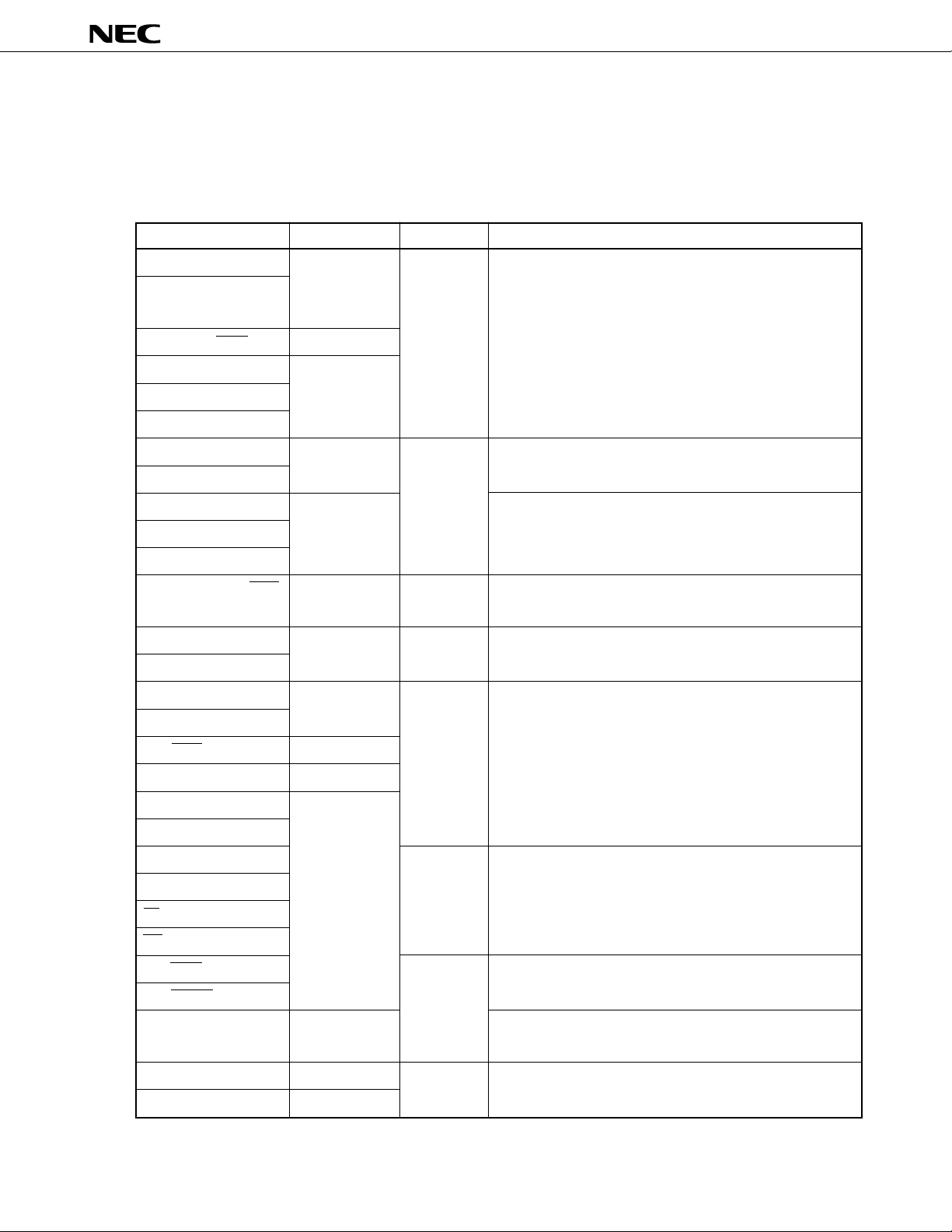
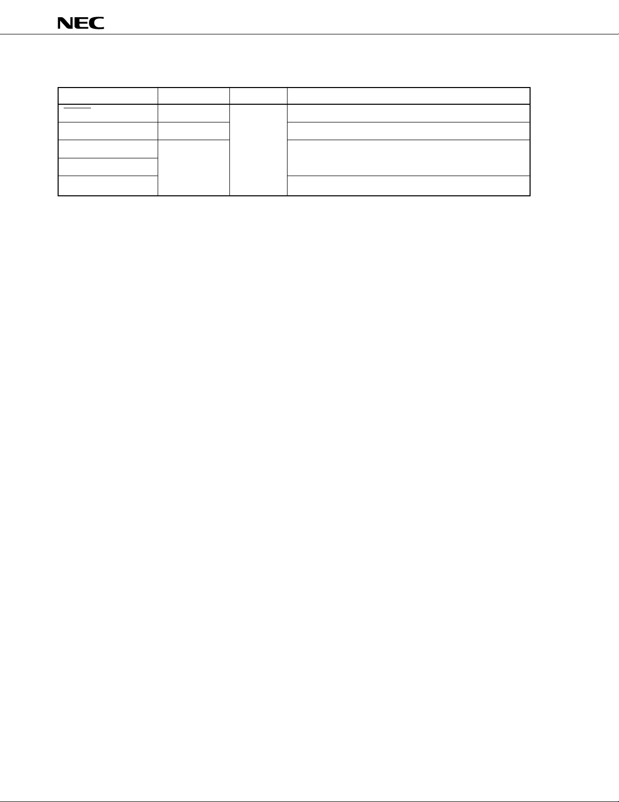
Table 6-1 describes the types of I/O circuits for pins and the handling of unused pins.
Fig. 6-1 shows the configuration of these various types of I/O circuits.
Table 6-1 Types of I/O Circuits for Pins and Handling of Unused Pins (1/2)
Pin I/O circuit type I/O Recommended connection method for unused pins
P00-P07 5-A I/O Input state : To be connected to VDD
P10/PWM0 Output state: To be left open
P11/PWM1
P12/ASCK2/SCK2 8-A
P13/RxD2/SI2 5-A
P14/TxD2/SO2
P15-P17
P20/NMI 2 Input To be connected to VDD or VSS
P21/INTP0
P22/INTP1 2-A To be connected to VDD
P23/INTP2/CI
P24/INTP3
P25/INTP4/ASCK/SCK1 8-A I/O Input state : To be connected to VDD
Output state: To be left open
P26/INTP5 2-A Input To be connected to VDD
P27/SI0
P30/RxD/SI1 5-A I/O Input state : To be connected to VDD
P31/TxD/SO1 Output state: To be left open
P32/SCK0 8-A
P33/SO0/SB0 10-A
P34/TO0-P37/TO3 5-A
AD0-AD7
A8-A15 Output
P60/A16-P63/A19
RD
WR
Note
To be left open
P66/WAIT/HLDRQ I/O Input state : To be connected to VDD
P67/REFRQ/HLDAK Output state: To be left open
P70/ANI0-P77/ANI7 20 Input state : To be connected to VDD or VSS
Output state: To be left open
ANO0, ANO1 12 Output To be left open
ASTB 4
Note These pins function as output-only pins depending on the internal circuit, though their I/O type is 5-A.
15
mm
m
PD784020, 784021
mm
Table 6-1 Types of I/O Circuits for Pins and Handling of Unused Pins (2/2)
Pin I/O circuit type I/O Recommended connection method for unused pins
RESET 2 Input —
TEST 1 To be connected to VSS directly
AVREF1-AVREF3 — To be connected to VSS
AVSS
AVDD To be connected to VDD
Caution When the I/O mode of an I/O dual-function pin is unpredictable, connect the pin to VDD through
a resistor of 10 to 100 kilohms (particularly when the voltage of the reset input pin becomes higher
than that of the low level input at power-on or when I/O is switched by software).
Remark Since type numbers are consistent in the 78K series, those numbers are not always serial in each product.
(Some circuits are not included.)
16
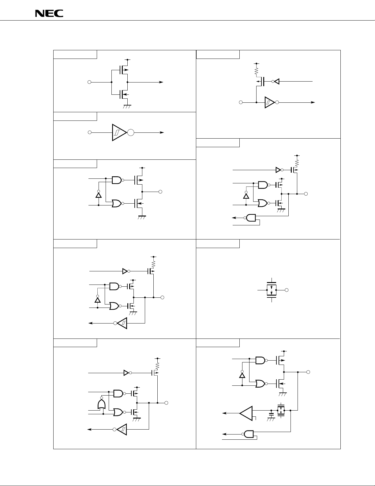
Fig. 6-1 I/O Circuits for Pins
mm
m
PD784020, 784021
mm
Type 1 Type 2-A
IN
Type 2
IN
Schmitt trigger input with hysteresis characteristics
Type 4
Data
DD
V
P
N
Type 5-A
DD
V
P
OUT
Output
disable
N
Push-pull output which can output high impedance
(both the positive and negative channels are off.)
Type 8-A
VDD
Type 12
V
DD
P
IN
Schmitt trigger input with hysteresis characteristics
V
Pull-up
enable
Data
Output
disable
Input
enable
DD
V
P
N
Pull-up
enable
DD
P
IN/OUT
Pull-up
enable
Output
disable
Type 10-A
Pull-up
enable
Open
drain
Output
disable
Data
Data
VDD
P
P
IN/OUT
N
Type 20
V
DD
P
V
DD
P
IN/OUT
N
Input
enable
Analog output
voltage
Data
Output
disable
Comparator
(Threshold voltage)
P
OUT
N
V
DD
P
IN/OUT
N
+
–
V
REF
P
N
17

mm
m
PD784020, 784021
mm
7. CPU ARCHITECTURE
7.1 MEMORY SPACE
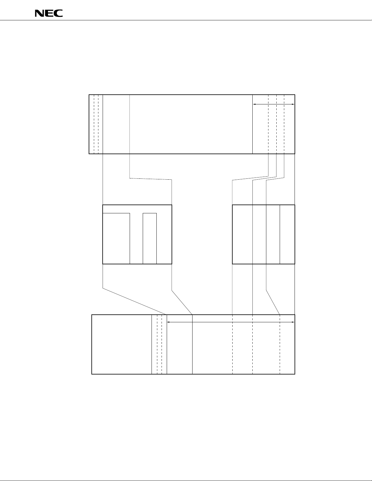
A 1M-byte memory space can be accessed. By using a LOCATION instruction, the mode for mapping internal
data areas (special function registers and internal RAM) can be selected. A LOCATION instruction must always be
executed after a reset, and can be used only once.
(1) When the LOCATION 0 instruction is executed
m
Internal data areas are mapped to 0FD00H-0FFFFH for the
(2) When the LOCATION 0FH instruction is executed
Internal data areas are mapped to FFD00H-FFFFFH for the
PD784020 and 0F700H-0FFFFH for the mPD784021.
m
PD784020 and FF700H-FFFFFH for the mPD784021.
18
mm
m
PD784020, 784021
mm
Note
(256 bytes)
Internal RAM
Special function registers (SFRs)
When the LOCATION 0FH
instruction is executed
FFFFFH
FFFDFH
FFFD0H
FFF00H
FFEFFH
HH
HH
H
FFEFFH
FFE80H
PD784020 Memory Map
mm
mm
m
Fig. 7-1
General-purpose
0FEFFH
0FE80H
(512 bytes)
FFD00H
FFCFFH
FFE7FH
FFE2FH
registers
(128 bytes)
FFE06H
Macro service control
0FE7FH
0FE2FH
0FE06H
FFD00H
Data area (512 bytes)
word area (42 bytes)
0FD00H
External memory
(1,047,808 bytes)
00FFFH
00FFFH
10000H
0FFFFH
00000H
00800H
007FFH
00080H
0007FH
CALLF entry area
(2K bytes)CALLT table area
00800H
007FFH
00080H
0007FH
(64 bytes)
Vector table area
(64 bytes)
00040H
0003FH
00000H
External memory
(960K bytes)
When the LOCATION 0
instruction is executed
FFFFFH
10000H
(256 bytes)
Internal RAM
(512 bytes)
Special function registers (SFRs)
0FFFFH
0FFDFH
0FFD0H
0FF00H
0FEFFH
0FD00H
0FCFFH
00000H
Note
External memory
(64,768 bytes)
Note Base area, or entry area based on a reset or interrupt. Internal RAM is excluded in the case of a reset.
19

(256 bytes)
Internal RAM
(2,048 bytes)
Special function registers (SFRs)
When the LOCATION 0FH
instruction is executed
External memory
(1,046,272 bytes)
mm
m
PD784020, 784021
mm
Note
FFFFFH
FFFDFH
FFFD0H
FFF00H
FFEFFH
FF700H
FFEFFH
FFE80H
General-purpose
PD784021 Memory Map
mm
mm
m
Fig. 7-2
registers
0FEFFH
0FE80H
FF6FFH
FFE7FH
FFE2FH
(128 bytes)
0FE7FH
0FE2FH
FFE06H
Macro service control
0FE06H
FFD00H
FFCFFH
FF700H
Program/data area
(1,536 bytes)
Data area (512 bytes)
word area (42 bytes)
0FD00H
0FCFFH
0F700H
00FFFH
00FFFH
00800H
CALLF entry area
00800H
Note
10000H
0FFFFH
007FFH
00080H
0007FH
(2K bytes)CALLT table area
007FFH
00080H
0007FH
00000H
(64 bytes)
Vector table area
(64 bytes)
00040H
0003FH
00000H
20
External memory
(960K bytes)
When the LOCATION 0
instruction is executed
FFFFFH
(256 bytes)
Internal RAM
(2,048 bytes)
Special function registers (SFRs)
10000H
0FFFFH
0FFDFH
0FFD0H
0FF00H
0FEFFH
0FD00H
0FCFFH
0F700H
0F6FFH
External memory
(63,232 bytes)
00000H
Note Base area, or entry area based on a reset or interrupt. Internal RAM is excluded in the case of a reset.
mm
m
PD784020, 784021
mm
7.2 CPU REGISTERS
7.2.1 General-Purpose Registers
A set of general-purpose registers consists of sixteen general-purpose 8-bit registers. Two 8-bit general-purpose
registers can be combined to form a 16-bit general-purpose register. Moreover, four 16-bit general-purpose registers,
when combined with an 8-bit register for address extension, can be used as 24-bit address specification registers.
Eight banks of this register set are provided. The user can switch between banks by software or the context
switching function.
General-purpose registers other than the V, U, T, and W registers used for address extension are mapped onto
internal RAM.
Fig. 7-3 General-Purpose Register Format
A (R1) X (R0)
AX (RP0)
B (R3) C (R2)
BC (RP1)
R5 R4
RP2
R7 R6
RP3
V
VVP (RG4)
U
UUP (RG5)
T
TDE (RG6)
W L (R14)
WHL (RG7)
The character strings enclosed in
parentheses represent absolute names.
R9 R8
VP (RP4)
R11 R10
UP (RP5)
D (R13) E (R12)
DE (RP6)
H (R15)
HL (RP7)
8 banks
Caution By setting the RSS bit of PSW to 1, R4, R5, R6, R7, RP2, and RP3 can be used as the X, A, C, B,
AX, and BC registers, respectively. However, this function must be used only when using
programs for the 78K/III series.
21

mm
m
PD784020, 784021
mm
7.2.2 Control Registers
(1) Program counter (PC)
This register is a 20-bit program counter. The program counter is automatically updated by program execution.
Fig. 7-4 Format of Program Counter (PC)
19 0
PC
(2) Program Status Word (PSW)
This register holds the CPU state. The program status word is automatically updated by program execution.
Fig. 7-5 Format of Program Status Word (PSW)
15 14 13 12
PSWH
PSW
PSWL
Note This flag is used to maintain compatibility with the 78K/III series. This flag must be set to 0 when programs
for the 78K/III series are being used.
(3) Stack pointer (SP)
This register is a 24-bit pointer for holding the start address of the stack. The high-order 4 bits must be set
to 0.
PC 0 0 0 0
UF RBS2 RBS1 RBS0
76543210
Note
S Z RSS
Fig. 7-6 Format of Stack Pointer (SP)
23 20 0
AC IE P/V 0 CY
11 10 9 8
22

mm
m
PD784020, 784021
mm
7.2.3 Special Function Registers (SFRs)
The special function registers are registers with special functions such as mode registers and control registers
for built-in peripheral hardware. The special function registers are mapped onto the 256-byte space between 0FF00H
Note
and 0FFFFH
Note Applicable when the LOCATION 0 instruction is executed. FFF00H-FFFFFH when the LOCATION 0FH
Caution Never attempt to access addresses in this area where no SFR is allocated. Otherwise, the
Table 7-1 lists the special function registers (SFRs). The titles of the table columns are explained below.
.
instruction is executed.
mm
m
PD784021 may be placed in the deadlock state. The deadlock state can be cleared only by a
mm
reset.
• Abbreviation ................... Symbol used to represent a built-in SFR. The abbreviations listed in the table are
reserved words for the NEC assembler (RA78K4). The C compiler (CC78K4) allows
the abbreviations to be used as sfr variables of bit type with the #pragma sfr command.
• R/W ................................. Indicates whether each SFR allows read and/or write operations.
R/W : Allows both read and write operations.
R : Allows read operations only.
W : Allows write operations only.
• Manipulatable bits .......... Indicates the maximum number of bits that can be manipulated whenever an SFR is
manipulated. An SFR that supports 16-bit manipulation can be described in the sf r
operand. For address specification, an even-numbered address must be specified.
An SFR that supports 1-bit manipulation can be described in a bit manipulation
instruction.
• When reset ..................... Indicates the state of each register when RESET is applied.
H
23

Table 7-1 Special Function Registers (SFRs) (1/4)
mm
m
PD784020, 784021
mm
Note
Address
0FF00H Port 0 P0 R/W ll – Undefined
0FF01H Port 1 P1 ll –
0FF02H Port 2 P2 R ll –
0FF03H Port 3 P3 R/W ll –
0FF06H Port 6 P6 ll – 00H
0FF07H Port 7 P7 ll – Undefined
0FF0EH Port 0 buffer register L P0L ll –
0FF0FH Port 0 buffer register H P0H ll –
0FF10H Compare register (timer/counter 0) CR00 – – l
0FF12H Capture/compare register (timer/counter 0) CR01 – – l
0FF14H Compare register L (timer/counter 1) CR10
0FF15H Compare register H (timer/counter 1) – – –
0FF16H Capture/compare register L (timer/counter 1) CR11
0FF17H Capture/compare register H (timer/counter 1) – – –
0FF18H Compare register L (timer/counter 2) CR20
0FF19H Compare register H (timer/counter 2) – – –
0FF1AH Capture/compare register L (timer/counter 2) CR21
Special function register (SFR) name Abbreviation R/W
CR10W
CR11W
CR20W
CR21W
Manipulatable bits
1 bit 8 bits 16 bits
– ll
– ll
– ll
– ll
When reset
0FF1BH Capture/compare register H (timer/counter 2) – – –
0FF1CH Compare register L (timer 3) CR30
0FF1DH Compare register H (timer 3) – – –
0FF20H Port 0 mode register PM0 ll – FFH
0FF21H Port 1 mode register PM1 ll –
0FF23H Port 3 mode register PM3 ll –
0FF26H Port 6 mode register PM6 ll –
0FF27H Port 7 mode register PM7 ll –
0FF2EH Real-time output port control register RTPC ll – 00H
0FF30H Capture/compare control register 0 CRC0 – l – 10H
0FF31H Timer output control register TOC ll – 00H
0FF32H Capture/compare control register 1 CRC1 – l –
0FF33H Capture/compare control register 2 CRC2 – l – 10H
CR30W
– ll
Note Applicable when the LOCATION 0 instruction is executed. When the LOCATION 0FH instruction is
executed, F0000H is added to each address.
24

mm
m
mm
Table 7-1 Special Function Registers (SFRs) (2/4)
PD784020, 784021
Address
0FF36H Capture register (timer/counter 0) CR02 R – – l 0000H
0FF38H Capture register L (timer/counter 1) CR12
0FF39H Capture register H (timer/counter 1) – – –
0FF3AH Capture register L (timer/counter 2) CR22
0FF3BH Capture register H (timer/counter 2) – – –
0FF41H Port 1 mode control register PMC1 R/W ll – 00H
0FF43H Port 3 mode control register PMC3 ll –
0FF4EH Register for optional pull-up resistor PUO ll –
0FF50H Timer register 0 TM0 R – – l 0000H
0FF51H ––
0FF52H Timer register 1 TM1 TM1W – ll
0FF53H – – –
0FF54H Timer register 2 TM2 TM2W – ll
0FF55H – – –
0FF56H Timer register 3 TM3 TM3W – ll
0FF57H – – –
Note
Special function register (SFR) name Abbreviation R/W
CR12W
CR22W
Manipulatable bits
1 bit 8 bits 16 bits
– ll
– ll
When reset
0FF5CH Prescaler mode register 0 PRM0 R/W – l – 11H
0FF5DH Timer control register 0 TMC0 ll – 00H
0FF5EH Prescaler mode register 1 PRM1 – l – 11H
0FF5FH Timer control register 1 TMC1 ll– 00H
0FF60H D/A conversion value setting register 0 DACS0 – l –
0FF61H D/A conversion value setting register 1 DACS1 – l –
0FF62H D/A converter mode register DAM ll – 03H
0FF68H A/D converter mode register ADM ll – 00H
0FF6AH A/D conversion result register ADCR R – l – Undefined
0FF70H PWM control register PWMC R/W ll– 05H
0FF71H PWM prescaler register PWPR – l – 00H
0FF72H PWM modulo register 0 PWM0 – – l Undefined
0FF74H PWM modulo register 1 PWM1 – – l
0FF7DH One-shot pulse output control register OSPC ll– 00H
0FF80H Serial bus interface control register SBIC ll –
0FF82H Synchronous serial interface mode register CSIM ll –
Note Applicable when the LOCATION 0 instruction is executed. When the LOCATION 0FH instruction is
executed, F0000H is added to each address.
25

Table 7-1 Special Function Registers (SFRs) (3/4)
mm
m
PD784020, 784021
mm
Note 1
Address
0FF84H Synchronous serial interface mode register 1 CSIM1 R/W ll – 00H
0FF85H Synchronous serial interface mode register 2 CSIM2 ll –
0FF86H Serial shift register SIO – l –
0FF88H Asynchronous serial interface mode register ASIM ll –
0FF89H Asynchronous serial interface mode register 2 ASIM2 ll –
0FF8AH Asynchronous serial interface status register ASIS R ll–
0FF8BH Asynchronous serial interface status register 2 ASIS2 ll –
0FF8CH Serial receive buffer: UART0 RXB – l – Undefined
0FF8DH Serial receive buffer: UART2 RXB2 R – l –
0FF90H Baud rate generator control register BRGC – l – 00H
0FF91H Baud rate generator control register 2 BRGC2 – l –
0FFA0H External interrupt mode register 0 INTM0 ll –
0FFA1H External interrupt mode register 1 INTM1 ll –
Special function register (SFR) name Abbreviation R/W
Serial transmission shift register: UART0 TXS W – l –
Serial shift register: IOE1 SIO1 R/W – l –
Serial transmission shift register: UART2 TXS2 W – l –
Serial shift register: IOE2 SIO2 R/W – l –
Manipulatable bits
1 bit 8 bits 16 bits
When reset
0FFA4H Sampling clock selection register SCS0 – l –
0FFA8H In-service priority register ISPR R ll –
0FFAAH Interrupt mode control register IMC R/W ll – 80H
0FFACH Interrupt mask register 0L MK0L MK0 ll lFFFFH
0FFADH Interrupt mask register 0H MK0H ll
0FFAEH Interrupt mask register 1L MK1L ll – FFH
0FFC0H Standby control register STBC – l
0FFC2H Watchdog timer mode register WDM – l
0FFC4H Memory expansion mode register MM ll – 20H
0FFC5H Hold mode register HLDM ll – 00H
0FFC6H Clock output mode register CLOM ll –
0FFC7H Programmable wait control register 1 PWC1 – l – AAH
0FFC8H Programmable wait control register 2 PWC2 – – l AAAAH
Note 2
Note 2
– 30H
– 00H
Notes 1. Applicable when the LOCATION 0 instruction is executed. When the LOCATION 0FH instruction is
executed, F0000H is added to each address.
2. A write operation can be performed only with special instructions MOV STBC,#byte and MOV
WDM,#byte. Other instructions cannot perform a write operation.
26
mm
m
mm
Table 7-1 Special Function Registers (SFRs) (4/4)
PD784020, 784021
Address
0FFCCH Refresh mode register RFM R/W ll – 00H
0FFCDH Refresh area specification register RFA ll –
0FFCFH Oscillation settling time specification register OSTS – l –
0FFD0H- External SFR area – ll– –
0FFDFH
0FFE0H Interrupt control register (INTP0) PIC0 ll – 43H
0FFE1H Interrupt control register (INTP1) PIC1 ll –
0FFE2H Interrupt control register (INTP2) PIC2 ll –
0FFE3H Interrupt control register (INTP3) PIC3 ll –
0FFE4H Interrupt control register (INTC00) CIC00 ll–
0FFE5H Interrupt control register (INTC01) CIC01 ll–
0FFE6H Interrupt control register (INTC10) CIC10 ll–
0FFE7H Interrupt control register (INTC11) CIC11 ll–
0FFE8H Interrupt control register (INTC20) CIC20 ll–
0FFE9H Interrupt control register (INTC21) CIC21 ll–
0FFEAH Interrupt control register (INTC30) CIC30 ll –
0FFEBH Interrupt control register (INTP4) PIC4 ll –
Note
Special function register (SFR) name Abbreviation R/W
Manipulatable bits
1 bit 8 bits 16 bits
When reset
0FFECH Interrupt control register (INTP5) PIC5 ll –
0FFEDH Interrupt control register (INTAD) ADIC ll–
0FFEEH Interrupt control register (INTSER) SERIC ll–
0FFEFH Interrupt control register (INTSR) SRIC ll –
Interrupt control register (INTCSI1) CSIIC1 ll–
0FFF0H Interrupt control register (INTST) STIC ll –
0FFF1H Interrupt control register (INTCSI) CSIIC ll –
0FFF2H Interrupt control register (INTSER2) SERIC2 ll–
0FFF3H Interrupt control register (INTSR2) SRIC2 ll –
Interrupt control register (INTCSI2) CSIIC2 ll–
0FFF4H Interrupt control register (INTST2) STIC2 ll –
Note Applicable when the LOCATION 0 instruction is executed. When the LOCATION 0FH instruction is
executed, F0000H is added to each address.
27
 Loading...