NEC UPD75P0016GB-3BS-MTX, UPD75P0016CU Datasheet

DATA SHEET
MOS INTEGRATED CIRCUIT
µ
PD75P0016
4-BIT SINGLE-CHIP MICROCONTROLLER
The µPD75P0016 replaces the µPD750008’s internal mask ROM with a one-time PROM and features expanded
ROM capacity.
µ
Because the
development using the µPD750004, 750006, or 750008 products, and for use in small-lot production.
Detailed information about product features and specifications can be found in the following document
PD75P0016 supports programming by users, it is suitable for use in prototype testing for system
µ
PD750008 User's Manual: U10740E
FEATURES
• Compatible with µPD750008
• Memory capacity:
• PROM : 16384 × 8 bits
• RAM : 512 × 4 bits
µ
• Can operate in same power supply voltage as the mask ROM version
DD = 2.2 to 5.5 V
• V
• Supports QTOP™ microcontroller
Remark QTOP Microcontroller is the general name for a total support service that includes imprinting, marking,
screening, and verifying one-time PROM single-chip microcontrollers offered by NEC.
ORDERING INFORMATION
Part number Package ROM (× 8 bits)
µ
PD75P0016CU 42-pin plastic shrink DIP (600 mil, 1.778-mm pitch) 16384
µ
PD75P0016GB-3BS-MTX 44-pin plastic QFP (10 × 10 mm, 0.8-mm pitch) 16384
Caution On-chip pull-up resistors by mask option cannot be provided.
PD750008
Document No. U10328EJ3V1DS00 (3rd edition)
Date Published August 2000 N CP(K)
Printed in Japan
The information in this document is subject to change without notice.
The mark shows major revised points.
©
1995

µ
PD75P0016
FUNCTION LIST
Item Function
Instruction execution time • 0.95, 1.91, 3.81, 15.3 µs (main system clock: at 4.19 MHz operation)
• 0.67, 1.33, 2.67, 10.7 µs (main system clock: at 6.0 MHz operation)
• 122 µs (subsystem clock: at 32.768 kHz operation)
On-chip memory PROM 16384 × 8 bits
RAM 512 × 4 bits
General register • In 4-bit operation: 8 × 4 banks
• In 8-bit operation: 4 × 4 banks
I/O port CMOS input 8 Connection of on-chip pull-up resistor specifiable by software: 7
CMOS I/O 18 Direct LED drive capability
Connection of on-chip pull-up resistor specifiable by software: 18
N-ch open drain I/O 8 Direct LED drive capability
13 V withstand voltage
Total 34
Timer 4 channels
• 8-bit timer/event counter: 1 channel
• 8-bit timer counter: 1 channel
• Basic interval timer/watchdog timer: 1 channel
• Watch timer: 1 channel
Serial interface • 3-wire serial I/O mode ... Switching of MSB/LSB-first
• 2-wire serial I/O mode
• SBI mode
Bit sequential buffer (BSB) 16 bits
Clock output (PCL) • Φ, 524, 262, 65.5 kHz (main system clock: at 4.19 MHz operation)
• Φ, 750, 375, 93.8 kHz (main system clock: at 6.0 MHz operation)
Buzzer output (BUZ) • 2, 4, 32 kHz (main system clock: at 4.19 MHz operation or subsystem clock:
at 32.768 kHz operation)
• 2.93, 5.86, 46.9 kHz (main system clock: at 6.0 MHz operation)
Vectored interrupt External: 3 Internal: 4
Test input External: 1 Internal: 1
System clock oscillation circuit • Main system clock oscillation ceramic/crystal oscillation circuit
• Subsystem clock oscillation crystal oscillation circuit
Standby function STOP/HALT mode
Operating ambient temperature TA = –40 to +85˚C
Supply voltage VDD = 2.2 to 5.5 V
Package 42-pin plastic shrink DIP (600 mil, 1.778-mm pitch)
44-pin plastic QFP (10 × 10 mm, 0.8-mm pitch)
2
Data Sheet U10328EJ3V1DS00

µ
PD75P0016
TABLE OF CONTENTS
1. PIN CONFIGURATION........................................................................................................................ 4
2. BLOCK DIAGRAM............................................................................................................................. 6
3. PIN FUNCTIONS................................................................................................................................ 7
3.1 Port Pins ..................................................................................................................................................... 7
3.2 Non-port Pins .............................................................................................................................................8
3.3 I/O Circuits for Pins ................................................................................................................................... 9
3.4 Handling of Unused Pins ........................................................................................................................ 11
4. SWITCHING BETWEEN MK I AND MK II MODES .......................................................................... 12
4.1 Differences between Mk I Mode and Mk II Mode................................................................................... 12
4.2 Setting of Stack Bank Selection (SBS) Register................................................................................... 13
5. DIFFERENCES BETWEEN µPD75P0016 AND µPD750004, 750006, AND 750008 ...................... 14
6. MEMORY CONFIGURATION ........................................................................................................... 15
7. INSTRUCTION SET .......................................................................................................................... 17
8. ONE-TIME PROM (PROGRAM MEMORY) WRITE AND VERIFY................................................... 28
8.1 Operation Modes for Program Memory Write/Verify ............................................................................ 28
8.2 Steps in Program Memory Write Operation .......................................................................................... 29
8.3 Steps in Program Memory Read Operation........................................................................................... 30
8.4 One-Time PROM Screening ..................................................................................................... ............... 31
9. ELECTRICAL SPECIFICATIONS.....................................................................................................32
10. CHARACTERISTIC CURVES (REFERENCE VALUE) .................................................................... 46
11. PACKAGE DRAWINGS .................................................................................................................... 48
12. RECOMMENDED SOLDERING CONDITIONS ................................................................................ 50
APPENDIX A. FUNCTION LIST OF µPD75008, 750008, 75P0016 ....................................................... 51
APPENDIX B. DEVELOPMENT TOOLS................................................................................................. 53
APPENDIX C. RELATED DOCUMENTS ................................................................................................ 57
Data Sheet U10328EJ3V1DS00
3
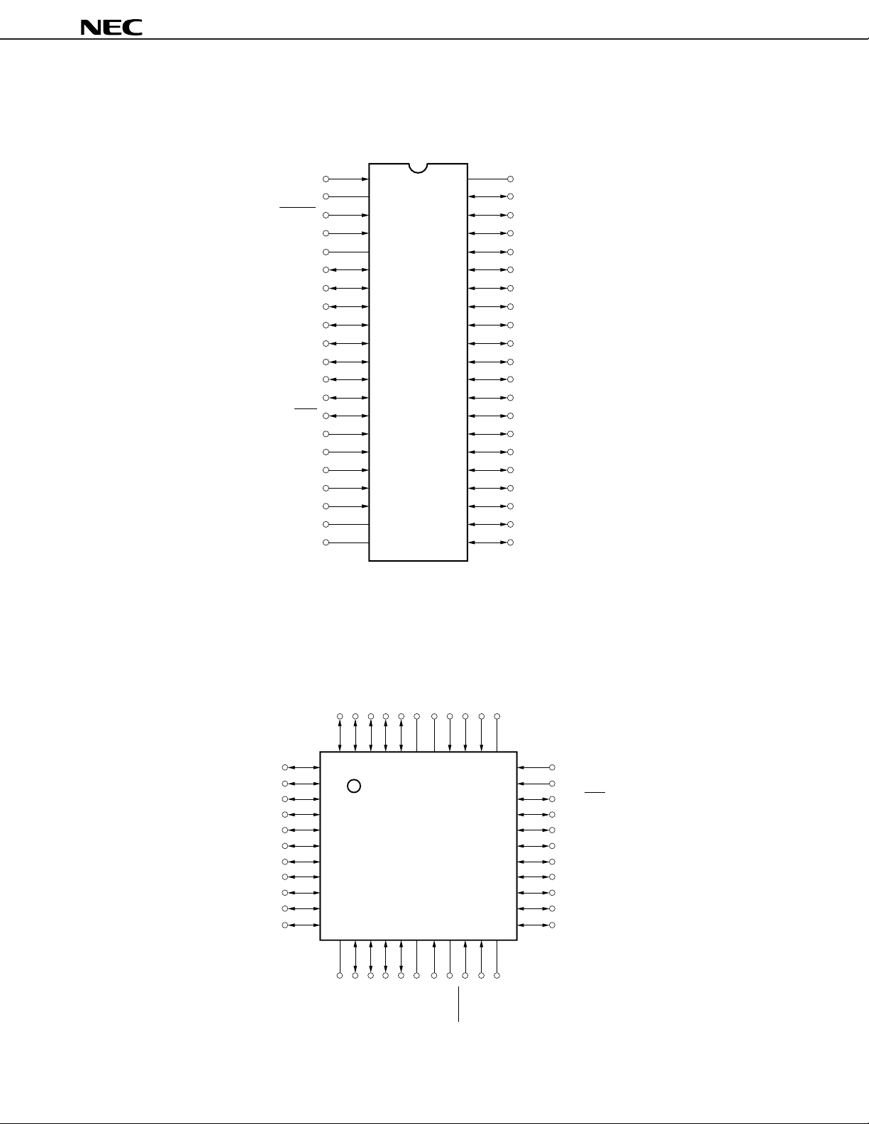
1. PIN CONFIGURATION (Top View)
•42-pin plastic shrink DIP (600 mil, 1.778-mm pitch)
µ
PD75P0016CU
µ
PD75P0016
XT1
XT2
RESET
X1
X2
P33/MD3
P32/MD2
P31/MD1
P30/MD0
P81
P80
P03/SI/SB1
P02/SO/SB0
P01/SCK
P00/INT4
P13/TI0
P12/INT2
P11/INT1
P10/INT0
Note
V
PP
V
DD
Note Directly connect V
V
1
2
3
4
5
6
7
8
9
10
11
12
13
14
15
16
17
18
19
20
21
PP to VDD in the normal operation mode.
42
41
40
39
38
37
36
35
34
33
32
31
30
29
28
27
26
25
24
23
22
SS
P40/D0
P41/D1
P42/D2
P43/D3
P50/D4
P51/D5
P52/D6
P53/D7
P60/KR0
P61/KR1
P62/KR2
P63/KR3
P70/KR4
P71/KR5
P72/KR6
P73/KR7
P20/PTO0
P21/PTO1
P22/PCL
P23/BUZ
• 44-pin plastic QFP (10 × 10 mm, 0.8-mm pitch)
µ
PD75P0016GB-3BS-MTX
P73/KR7
P20/PTO0
44
10
11
43
1
2
3
4
5
6
7
8
9
12
13
NC
P43/D3
P72/KR6
P71/KR5
P70/KR4
P63/KR3
P62/KR2
P61/KR1
P60/KR0
P53/D7
P52/D6
P51/D5
P50/D4
P21/PTO1
P22/PCL
42
41
14
15
P42/D2
P41/D1
P23/BUZ
40
39
16
17
P40/D0
DD
V
SS
V
Note
38
18
PP
V
P10/INT0
37
19
XT1
XT2
P11/INT1
36
35
20
21
RESET
P12/INT2
NC
34
33
32
31
30
29
28
27
26
25
24
23
22
X1
X2
P13/TI0
P00/INT4
P01/SCK
P02/SO/SB0
P03/SI/SB1
P80
P81
P30/MD0
P31/MD1
P32/MD2
P33/MD3
Note Directly connect V
4
Data Sheet U10328EJ3V1DS00
PP to VDD in the normal operation mode.

µ
PD75P0016
PIN IDENTIFICATIONS
P00-P03 : Port0 SCK : Serial Clock
P10-P13 : Port1 SI : Serial Input
P20-P23 : Port2 SO : Serial Output
P30-P33 : Port3 SB0, SB1 : Serial Data Bus 0,1
P40-P43 : Port4 RESET : Reset
P50-P53 : Port5 TI0 : Timer Input 0
P60-P63 : Port6 PTO0, PTO1 : Programmable Timer Output 0, 1
P70-P73 : Port7 BUZ : Buzzer Clock
P80, P81 : Port8 PCL : Programmable Clock
KR0-KR7 : Key Return 0-7 INT0, 1, 4 : External Vectored Interrupt 0, 1, 4
DD : Positive Power Supply INT2 : External Test Input 2
V
VSS : Ground X1, X2 : Main System Clock Oscillation 1, 2
PP : Programming Power Supply XT1, XT2 : Subsystem Clock Oscillation 1, 2
V
NC : No Connection MD0-MD3 : Mode Selection 0-3
D0-D7 : Data Bus 0-7
Data Sheet U10328EJ3V1DS00
5
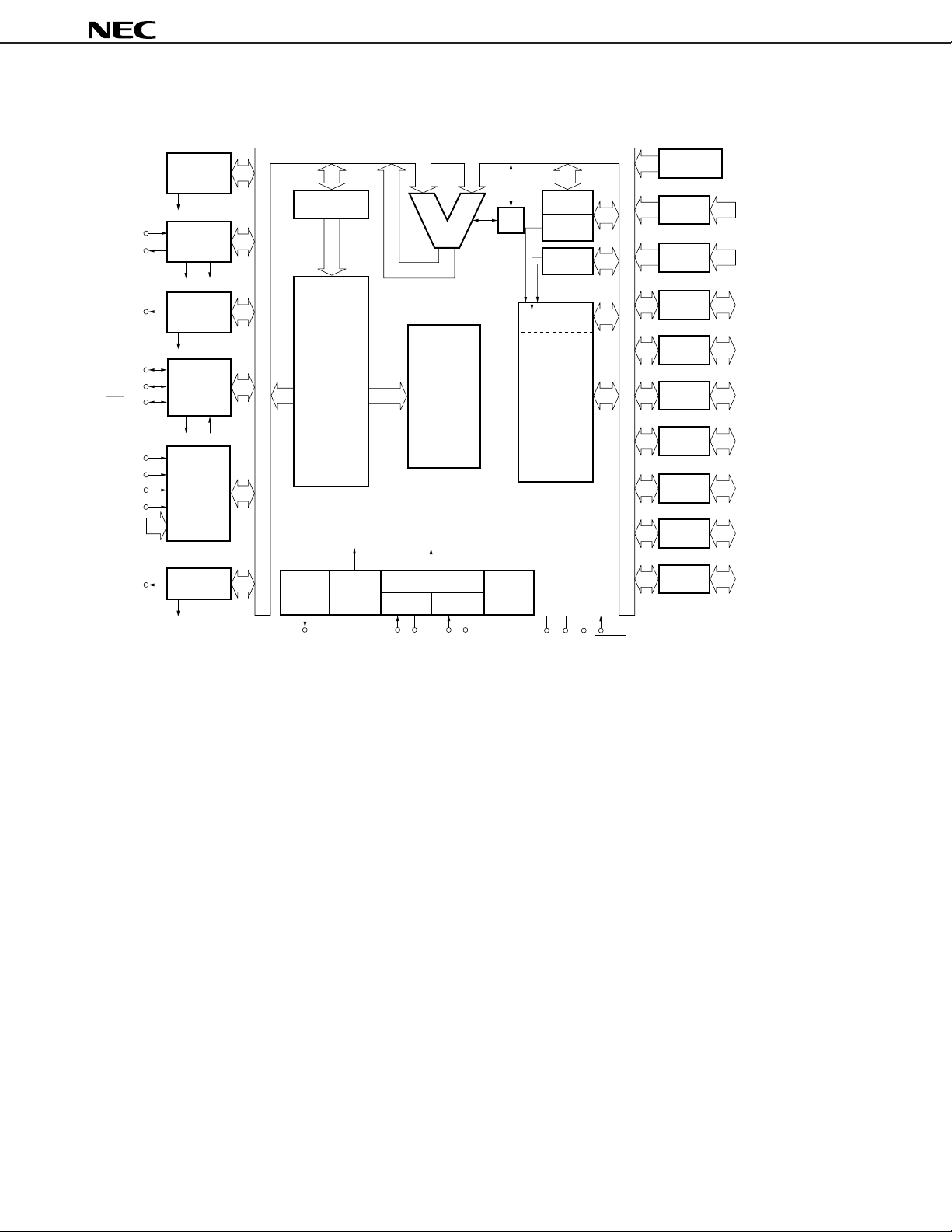
2. BLOCK DIAGRAM
µ
PD75P0016
TI0/P13
PTO0/P20
PTO1/P21
SI/SB1/P03
SO/SB0/P02
SCK/P01
INT0/P10
INT1/P11
INT2/P12
INT4/P00
KR0/P60KR7/P73
BUZ/P23
BASIC INTERVAL
TIMER/
WATCHDOG
TIMER
8-BIT
TIMER/EVENT
COUNTER #0
INTT0
8-BIT TIMER
COUNTER
CLOCKED
SERIAL
INTERFACE
INTCSI
INTERRUPT
CONTROL
8
INTBT
#1
INTT1
WATCH
TIMER
INTW
TOUT0
TOUT0
PROGRAM
COUNTER (14)
PROGRAM
MEMORY
(PROM)
16384 × 8 BITS
CLOCK
OUTPUT
CONTROL
fx/2
CLOCK
DIVIDER
N
SYSTEM CLOCK
GENERATOR
ALU
DECODE
AND
CONTROL
CPU CLOCK
Φ
MAINSUB
CY
STAND BY
CONTROL
SP (8)
SBS
BANK
GENERAL
REGISTER
DATA
MEMORY
(RAM)
512 × 4 BITS
BIT SEQ.
BUFFER (16)
PORT0 P00-P034
PORT1
PORT2 4
PORT3 P30/MD0-P33/MD34
PORT4 P40/D0-P43/D34
PORT5 P50/D4-P53/D74
PORT6 P60-P634
PORT7 P70-P734
PORT8 P80, P812
P10-P134
P20-P23
PCL/P22
X2X1XT2XT1
VSSVDD RESETVPP
6
Data Sheet U10328EJ3V1DS00
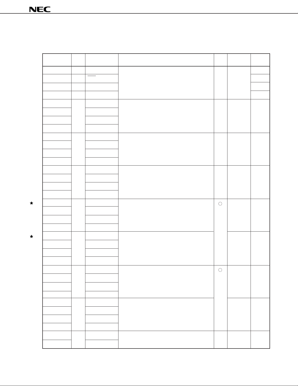
3. PIN FUNCTIONS
3.1 Port Pins
µ
PD75P0016
Pin name I/O Shared by Function 8-bit When I/O circuit
P00 I INT4 This is a 4-bit input port (PORT0). × Input <B>
P01 I/O SCK are software-specifiable in 3-bit units. <F>-A
P02 I/O SO/SB0 <F>-B
P03 I/O SI/SB1 <M>-C
P10 I INT0 This is a 4-bit input port (PORT1). × Input <B>-C
P11 INT1 specifiable in 4-bit units.
P12 INT2
P13 TI0
P20 I/O PTO0 This is a 4-bit I/O port (PORT2). × Input E-B
P21 PTO1 specifiable in 4-bit units.
P22 PCL
P23 BUZ
P30 I/O MD0 This is a programmable 4-bit I/O port (PORT3). × Input E-B
P31 MD1 units. On-chip pull-up resistor connections are
P32 MD2
P33 MD3
Note 2
P40
Note 2
P41
Note 2
P42
Note 2
P43
Note 2
P50
Note 2
P51
Note 2
P52
Note 2
P53
P60 I/O KR0 This is a programmable 4-bit I/O port (PORT6). Input <F>-A
P61 KR1 On-chip pull-up resistor connections are softwareP62 KR2
P63 KR3
I/O D0 This is an N-ch open-drain 4-bit I/O port (PORT4). High
D1
D2
D3
I/O D4 This is an N-ch open-drain 4-bit I/O port (PORT5). High
D5
D6
D7
For P01 to P03, on-chip pull-up resistor connections
On-chip pull-up resistor connections are softwareP10/INT0 can select noise elimination circuit.
On-chip pull-up resistor connections are software-
Input and output can be specified in single-bit
software-specifiable in 4-bit units.
In the open-drain mode, withstands up to 13 V. impedance M-E
In the open-drain mode, withstands up to 13 V. impedance M-E
Input and output can be specified in single-bit units.
specifiable in 4-bit units.
I/O reset type
Note 1
P70 I/O KR4 This is a 4-bit I/O port (PORT7). Input <F>-A
On-chip pull-up resistor connections are software-
P71 KR5 specifiable in 4-bit units.
P72 KR6
P73 KR7
P80 I/O — This is a 2-bit I/O port (PORT8). × Input E-B
On-chip pull-up resistor connections are software-
P81 — specifiable in 2-bit units.
Notes 1. Circuit types enclosed in brackets indicate Schmitt triggered inputs.
2. Low-level input current leakage increases when input instructions or bit manipulation instructions are executed.
Data Sheet U10328EJ3V1DS00
7
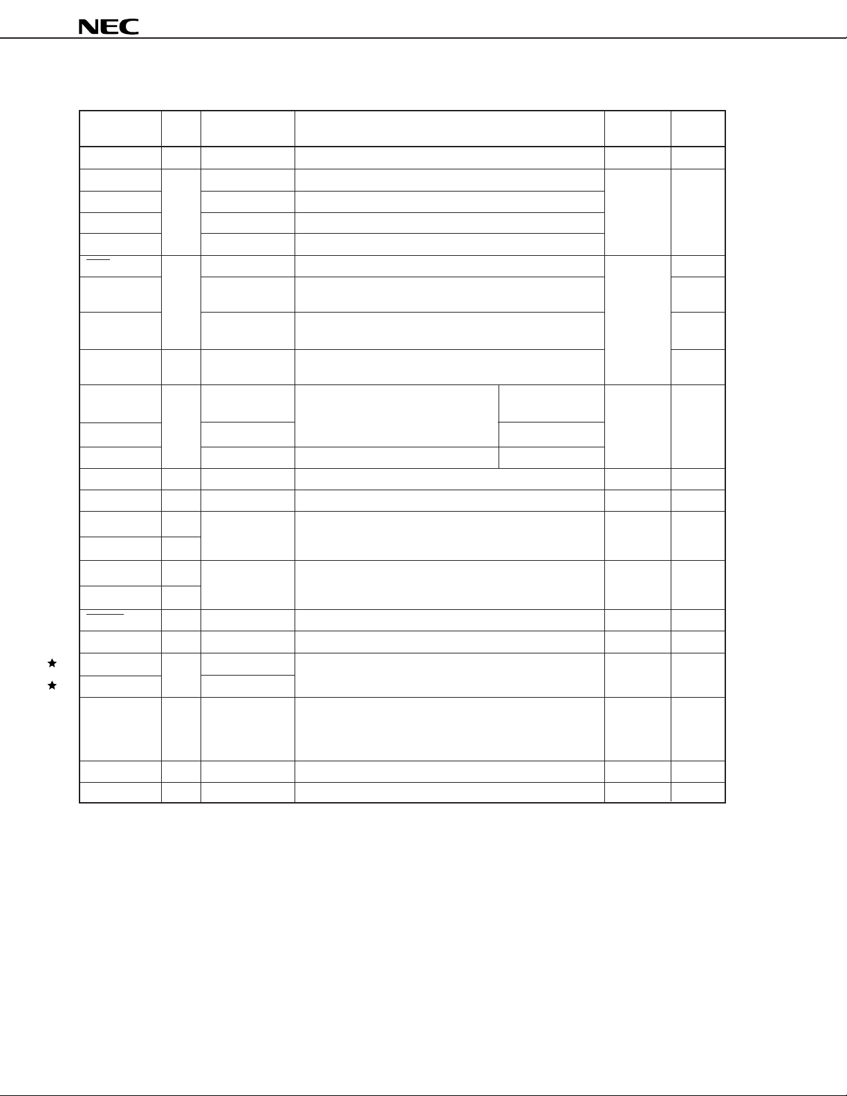
3.2 Non-port Pins
µ
PD75P0016
Pin name I/O Shared by Function When I/O circuit
TI0 I P13 External event pulse input to timer/event counter Input <B>-C
PTO0 O P20 Timer/event counter output Input E-B
PTO1 P21 Timer counter output
PCL P22 Clock output
BUZ P23 Outputs any frequency (for buzzer or system clock trimming)
SCK I/O P01 Serial clock I/O Input <F>-A
SO/SB0 P02 Serial data output <F>-B
SI/SB1 P03 Serial data input <M>-C
INT4 I P00 Edge-triggered vectored interrupt input <B>
INT0 I P10 Edge-triggered vectored interrupt input With noise eliminator Input <B>-C
INT1 P11 circuit. Asynch
INT2 P12 Rising edge-triggered testable input Asynch
KR0-KR3 I P60-P63 Falling edge-triggered testable input Input <F>-A
KR4-KR7 I P70-P73 Falling edge-triggered testable input Input <F>-A
X1 I — Ceramic/crystal resonator connection for main system clock. — —
X2 — inverted clock to X2.
XT1 I — Crystal resonator connection for subsystem clock. — —
XT2 — ed clock to X2. XT1 can be used as a 1-bit (test) input.
RESET I — System reset input (low level active) — <B>
MD0-MD3 I P30-P33 Mode selection for program memory (PROM) write/verify. Input E-B
D0-D3 I/O P40-P43 Data bus pin for program memory (PROM) write/verify. Input M-E
D4-D7 P50-P53
Note 2
VPP
VDD — — Positive power supply — —
VSS — — Ground potential — —
— — Programmable voltage supply in program memory (PROM) — —
Serial data bus I/O
Serial data bus I/O
(Detects both rising and falling edges).
(detected edge is selectable). /asynch selectable
INT0/P10 can select noise elimination
If using an external clock, input it to X1 and input the
If using an external clock, input it to XT1 and input the invert-
write/verify mode.
In normal operation mode, connect directly to VDD.
Apply +12.5 V in PROM write/verify mode.
reset type
Note 1
Notes 1. Circuit types enclosed in brackets indicate Schmitt triggered inputs.
2. During normal operation, the VPP pin will not operate normally unless connected to VDD pin.
8
Data Sheet U10328EJ3V1DS00
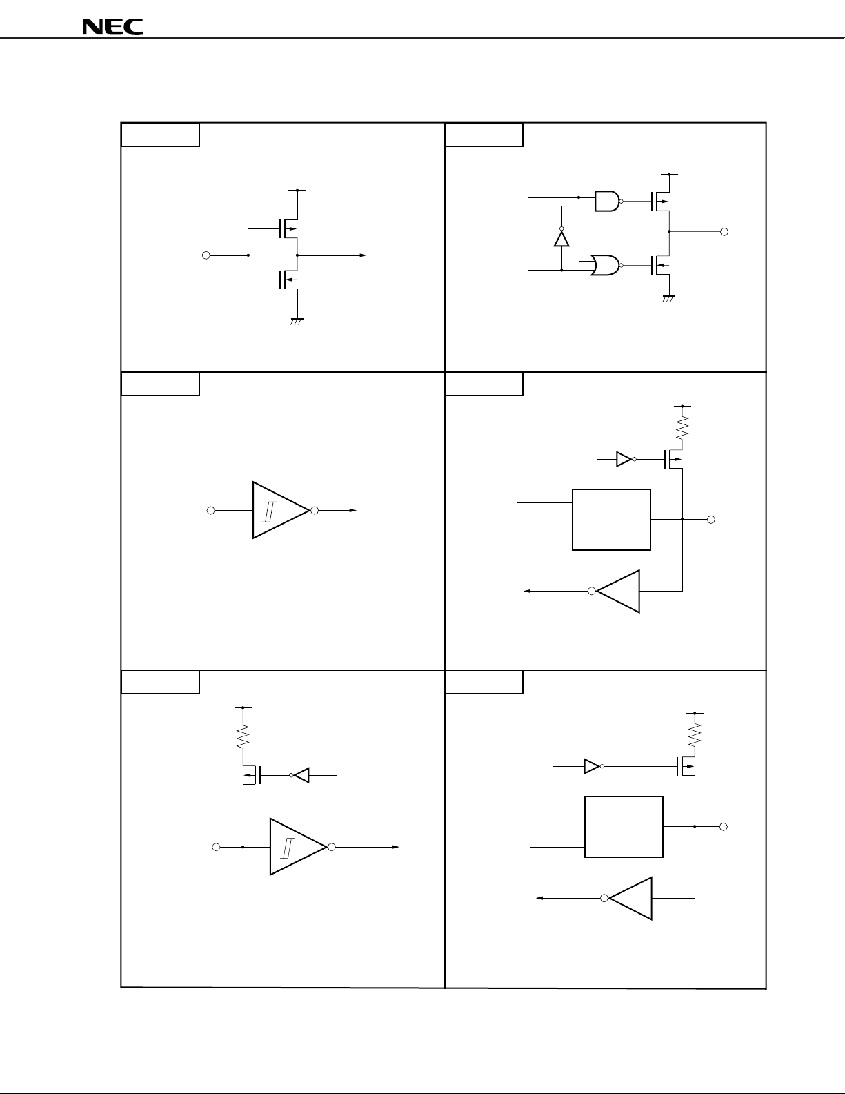
3.3 I/O Circuits for Pins
(
)
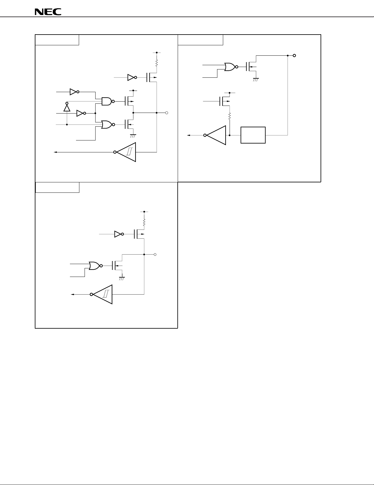
The I/O circuits for the µPD75P0016’s pin are shown in schematic diagrams below.
TYPE A TYPE D
V
DD
Data
IN
CMOS standard input buffer
P-ch
N-ch
Output
disable
Push-pull output that can be set to high impedance output
(with both P-ch and N-ch OFF).
µ
PD75P0016
V
DD
P-ch
OUT
N-ch
TYPE E-BTYPE B
IN
Output
disable
Schmitt trigger input with hysteresis characteristics.
TYPE B-C TYPE F-A
V
DD
P.U.R.
P-ch
P.U.R.
enable
Data
P.U.R.
enable
Type D
P.U.R. : Pull-Up Resistor
P.U.R.
enable
Type A
V
DD
P-ch
IN/OUT
V
DD
P.U.R.
P.U.R.
P-ch
IN
P.U.R. : Pull-Up Resistor
Data
Output
disable
Data Sheet U10328EJ3V1DS00
Type D
Type B
P.U.R. : Pull-Up Resistor
IN/OUT
Continued
9
µ
PD75P0016
TYPE F-B
output
disable
(P)
data
output
disable
TYPE M-C
output
disable
(N)
P.U.R.
enable
V
DD
P.U.R. : Pull-Up Resistor
P-ch
N-ch
V
TYPE M-E
V
DD
IN/OUT
P.U.R.
P-ch
IN/OUT
data
output
disable
Input
instruction
V
DD
P-ch
P.U.R.
N-ch
(+13 V)
Note
Voltage
limitation
circuit
(+13 V)
Note Pull-up resistor that operates only when an input
instruction has been executed. (Current flows
from V
DD
DD
to the pins when at low level)
data
output
disable
P.U.R.
enable
N-ch
P.U.R. : Pull-Up Resistor
P.U.R.
P-ch
IN/OUT
10
Data Sheet U10328EJ3V1DS00

3.4 Handling of Unused Pins
P00/INT4 Connect to VSS or VDD
P01/SCK Individually connect to VSS or VDD via resistor
P02/SO/SB0
P03/SI/SB1 Connect to VSS
P10/INT0-P12/INT2 Connect to VSS or VDD
P13/TI0
P20/PTO0
P21/PTO1
P22/PCL
P23/BUZ
P30/MD0-P33/MD3
P40/D0-P43/D3 Connect to VSS
P50/D4-P53/D7
P60/KR0-P63/KR3
P70/KR4-P73/KR7
P80, P81
Note
XT1
Note
XT2
VPP Make sure to connect directly to VDD
Table 3-1. Handling of Unused Pins
Pin Recommended connection
Input mode : individually connect to VSS or VDD
via resistor
Output mode : open
Input mode : individually connect to VSS or VDD
via resistor
Output mode : open
Connect to VSS
Open
µ
PD75P0016
Note When the subsystem clock is not used, set SOS. 0 to 1 (not to use the internal feedback resistor).
Data Sheet U10328EJ3V1DS00
11
µ
PD75P0016
4. SWITCHING BETWEEN MK I AND MK II MODES
Setting a stack bank selection (SBS) register for the µPD75P0016 enables the program memory to be switched
between the Mk I mode and the Mk II mode. This capability enables the evaluation of the µPD750004, 750006, or 750008
using the µPD75P0016.
µ
When the SBS bit 3 is set to 1: sets Mk I mode (corresponds to Mk I mode of
When the SBS bit 3 is set to 0: sets Mk II mode (corresponds to Mk II mode of µPD750004, 750006, and 750008)
4.1 Differences between Mk I Mode and Mk II Mode
Table 4-1 lists the differences between the Mk I mode and the Mk II mode of the
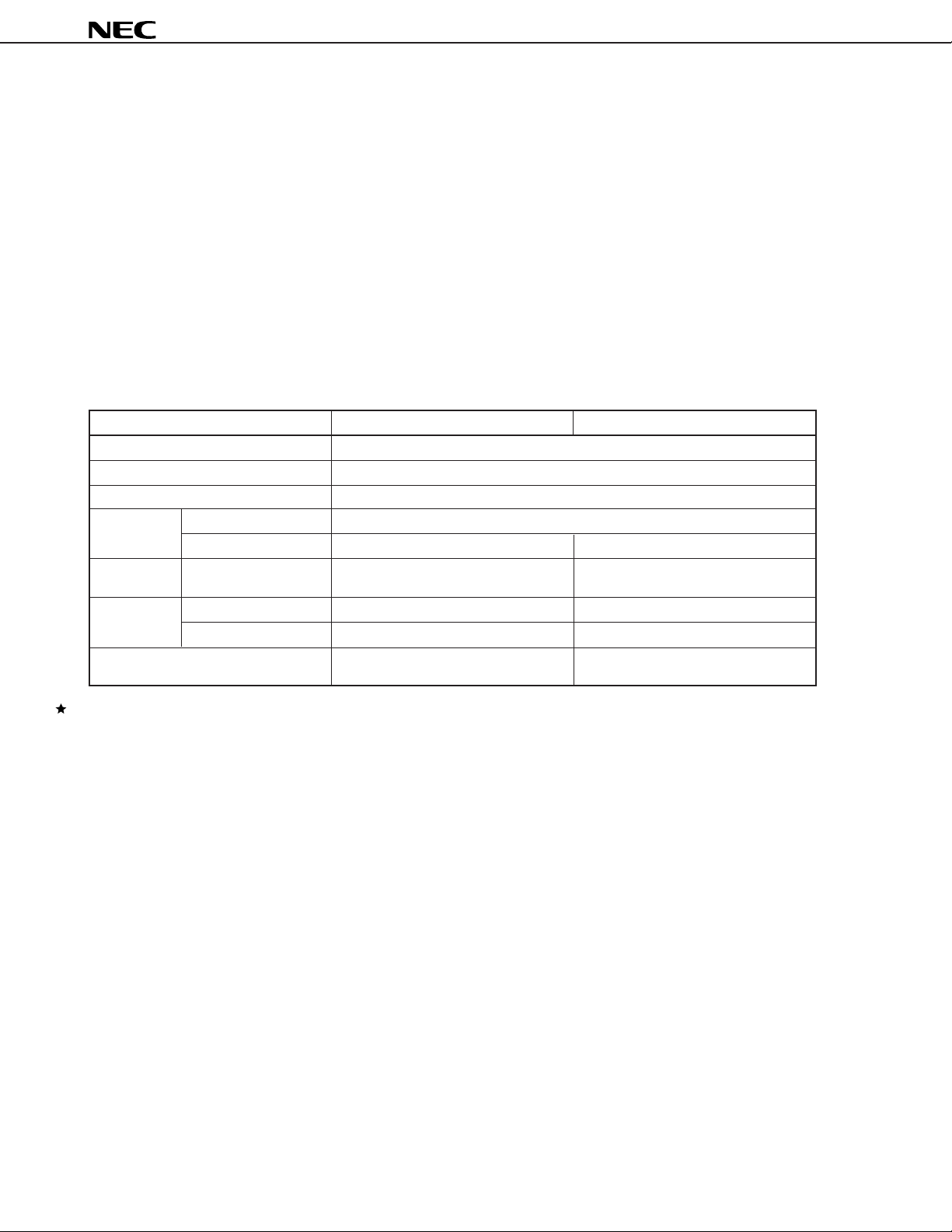
Table 4-1. Differences between Mk I Mode and Mk II Mode
Item Mk I mode Mk II mode
Program counter PC13-0
Program memory (bytes) 16384
Data memory (bits) 512 × 4
Stack Stack bank Selectable from memory banks 0 and 1
Stack bytes 2 bytes 3 bytes
Instruction BRA !addr1 None Provided
CALLA !addr1
Instruction CALL !addr 3 machine cycles 4 machine cycles
execution time CALLF !faddr 2 machine cycles 3 machine cycles
Supported mask ROM versions and Mk I mode of µPD750004, 750006, and Mk II mode of µPD750004, 750006, and
mode 750008 750008
PD750004, 750006, and 750008)
µ
PD75P0016.
Caution The Mk II mode supports a program area which exceeds 16K bytes in the 75X and 75XL series. This
mode enhances the software compatibility with products which have more than 16K bytes.
When the Mk II mode is selected, the number of stack bytes used in execution of a subroutine call
instruction increases by 1 per stack for the usable area compared to the Mk I mode. Furthermore, when
a CALL !addr, or CALLF !faddr instruction is used, each instruction takes another machine cycle.
Therefore, when more importance is attached to RAM utilization or throughput than software
compatibility, use the Mk I mode.
12
Data Sheet U10328EJ3V1DS00
µ
PD75P0016
4.2 Setting of Stack Bank Selection (SBS) Register
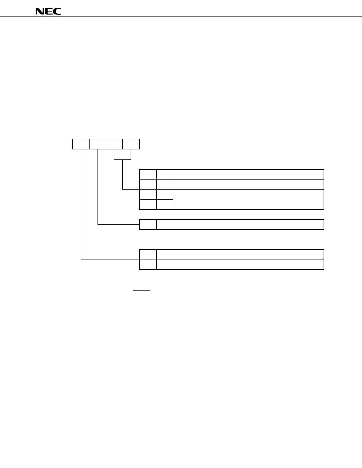
Use the stack bank selection register to switch between the Mk I mode and the Mk II mode. Figure 4-1 shows the format
for doing this.
The stack bank selection register is set using a 4-bit memory manipulation instruction. When using the Mk I mode,
Note
be sure to initialize the stack bank selection register to 100×B
Note
II mode, be sure to initialize it to 000×B
.
at the beginning of the program. When using the Mk
Note Set the desired value for ×.
Figure 4-1. Format of Stack Bank Selection Register
Address 3 2 1 0
SBS3 SBS2 SBS1 SBS0F84H
Symbol
SBS
Stack area specification
0
0
1
1
0 Be sure to set 0 for bit 2.
Memory bank 0
0
Memory bank 1
1
0
Setting prohibited
1
Mode selection specification
01Mk II mode
Mk I mode
Caution SBS3 is set to “1” after RESET input, and consequently the CPU operates in the Mk I mode. When using
instructions for the Mk II mode, set SBS3 to “0” to enter the Mk II mode before using the instructions.
Data Sheet U10328EJ3V1DS00
13
µ
PD75P0016
5. DIFFERENCES BETWEEN µPD75P0016 AND µPD750004, 750006, AND 750008
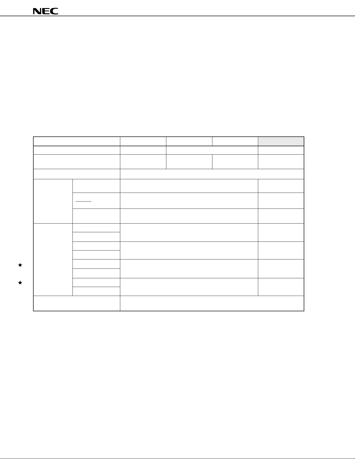
The µPD75P0016 replaces the internal mask ROM in the µPD750004, 750006, and 750008 with a one-time PROM
and features expanded ROM capacity. The µPD75P0016’s Mk I mode supports the Mk I mode in the µPD750004, 750006,
and 750008 and the µPD75P0016’s Mk II mode supports the Mk II mode in the µPD750004, 750006, and 750008.
µ
Table 5-2 lists differences among the
differences between corresponding versions beforehand, especially when a PROM version is used for debugging or
prototype testing of application systems and later the corresponding mask ROM version is used for full-scale production.
µ
Please refer to the
PD750008 User's Manual (U10740E) for details on CPU functions and on-chip hardware.
Table 5-1. Differences between
PD75P0016 and the µPD750004, 750006, and 750008. Be sure to check the
µ
PD75P0016 and µPD750004, 750006, and 750008
Item
Program counter 12-bit 13-bit 14-bit
Program memory (bytes) Mask ROM Mask ROM Mask ROM One-time PROM
Data memory (× 4 bits) 512
Mask options Pull-up resistor for Yes (On-chip/not on-chip can be specified.) No (On-chip not
port 4 and port 5 possible)
Wait time when Yes (217/fx or 215/fx)
RESET
Feedback resistor Yes (can select usable or unusable.) No (usable)
for subsystem clock
Pin connection Pins 6-9 (CU) P33-P30 P33/MD3-P30/MD0
Pins 23-26 (GB)
Pin 20 (CU) IC VPP
Pin 38 (GB)
Pins 34-37 (CU) P53-P50 P53/D7-P50/D4
Pins 8-11 (GB)
Pins 38-41 (CU) P43-P40 P43/D3-P40/D0
Pins 13-16 (GB)
Other Noise resistance and noise radiation may differ due to the different circuit complexities and
µ
PD750004
4096 6144 8192 16384
mask layouts.
Note
µ
PD750006
µ
PD750008
µ
No (fixed at 215/fx)
PD75P0016
Note
Note 217/fx : 21.8 ms @ 6.0 MHz, 31.3 ms @ 4.19 MHz
15
/fx : 5.46 ms @ 6.0 MHz, 7.81 ms @ 4.19 MHz
2
Caution Noise resistance and noise radiation are different in PROM version and mask ROM versions. If using
a mask ROM version instead of the PROM version for processes between prototype development and
full production, be sure to fully evaluate the CS of the mask ROM version (not ES).
14
Data Sheet U10328EJ3V1DS00
6. MEMORY CONFIGURATION
76 0
MBE
RBE
0000H
0002H
0004H
0006H
0008H
000AH
000CH
MBE
MBE
MBE
MBE
MBE
MBE
Internal reset start address (higher 6 bits)
Internal reset start address (lower 8 bits)
RBE
INTBT/INT4 start address (higher 6 bits)
INTBT/INT4 start address (lower 8 bits)
RBE
INT0 start address (higher 6 bits)
INT0 start address (lower 8 bits)
RBE
INT1 start address (higher 6 bits)
INT1 start address (lower 8 bits)
RBE
INTCSI start address (higher 6 bits)
INTCSI start address (lower 8 bits)
RBE
INTT0 start address (higher 6 bits)
INTT0 start address (lower 8 bits)
RBE
INTT1 start address (higher 6 bits)
INTT1 start address (lower 8 bits)
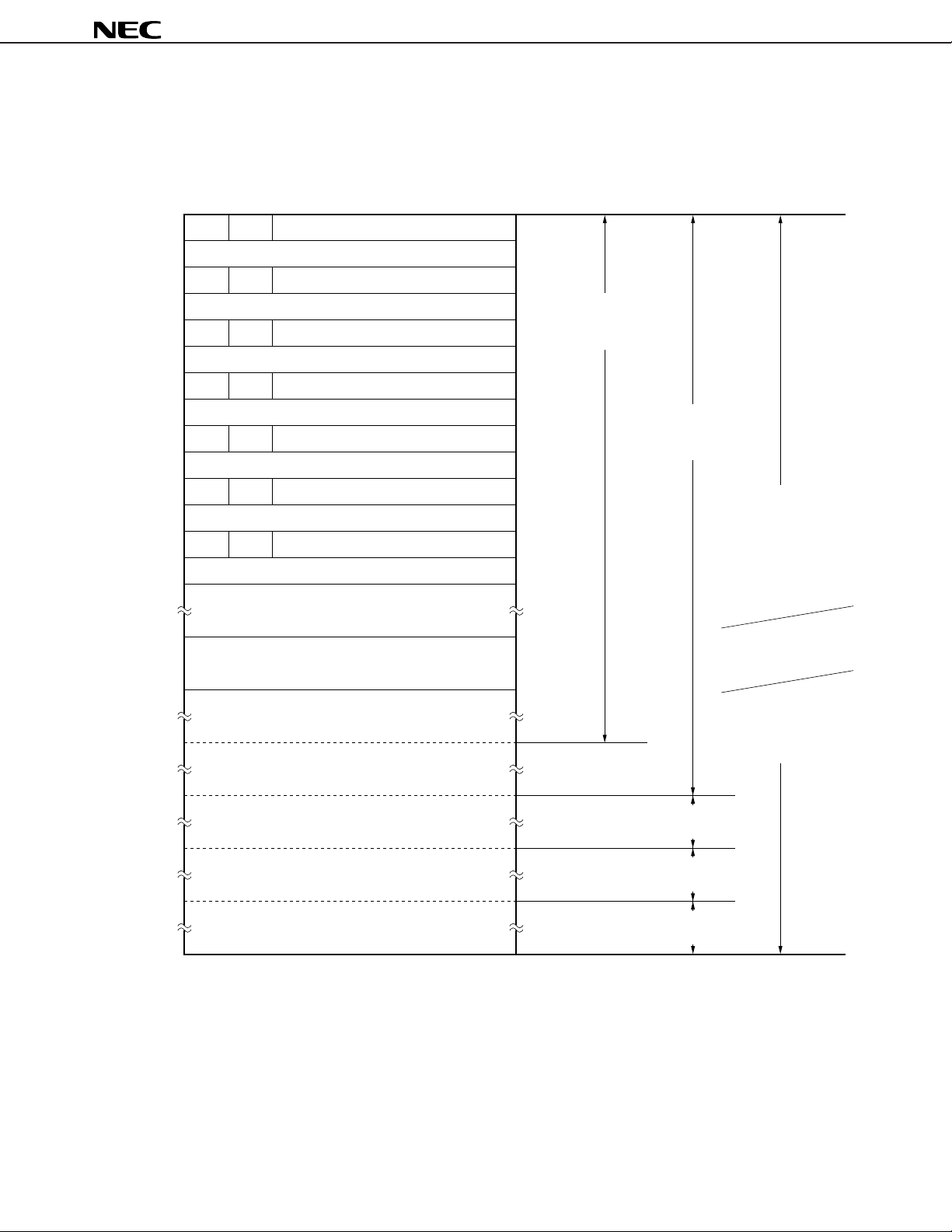
Figure 6-1. Program Memory Map
CALLF
!faddr instruction
entry address
BRCB
!caddr instruction
branch address
Branch address for
the following instructions
µ
PD75P0016
• BR BCDE
• BR BCXA
• BR !addr
• CALL !addr
• BRA !addr1
• CALLA !addr1
Note
Note
0020H
007FH
0080H
07FFH
0800H
0FFFH
1000H
1FFFH
2000H
2FFFH
3000H
3FFFH
Reference table for GETI instruction
BRCB
!caddr instruction
branch address
BRCB
!caddr instruction
branch address
BRCB
!caddr instruction
branch address
Branch/call
address
by GETI
BR $addr instruction
relative branch address
(–15 to –1,
+2 to +16)
Note Can be used only at Mk II mode.
Remark For instructions other than those noted above, the “BR PCDE” and “BR PCXA” instructions can be used to
branch to addresses with changes in the PC’s lower 8 bits only.
Data Sheet U10328EJ3V1DS00
15
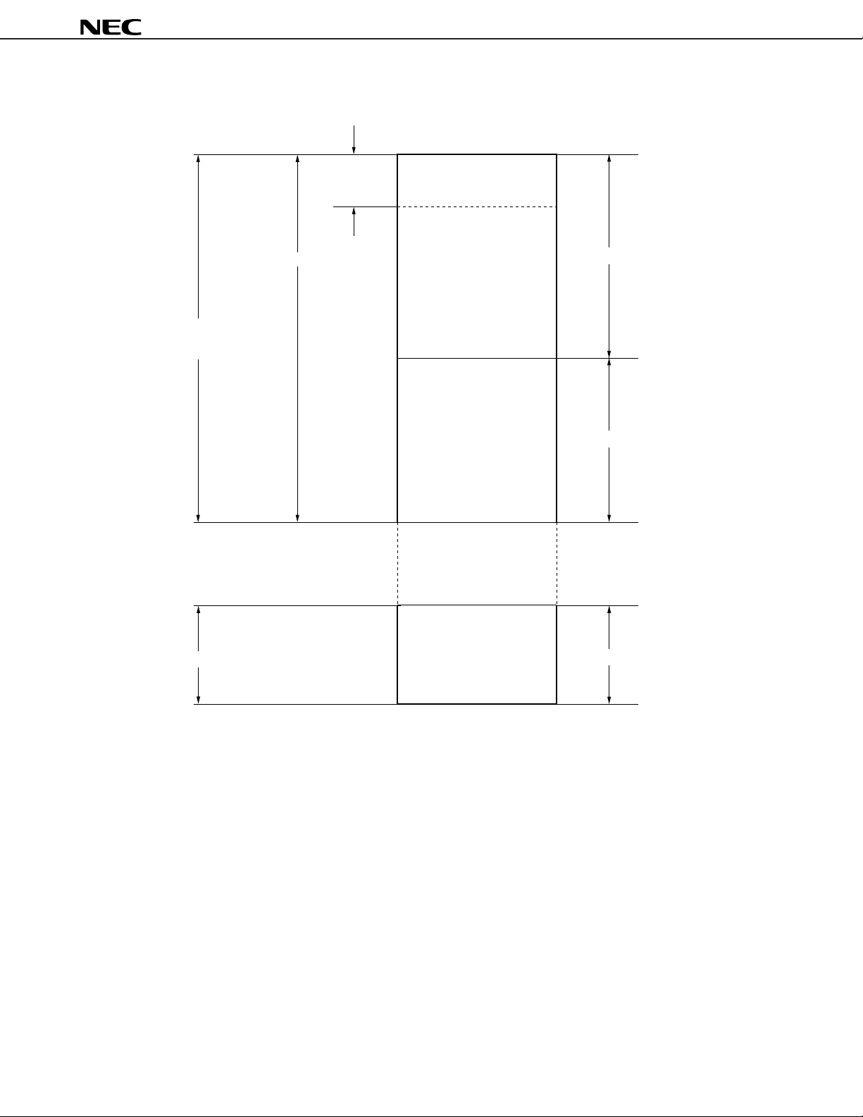
Figure 6-2. Data Memory Map
µ
PD75P0016
Data area
static RAM
(512 × 4)
General
register
Stack area
area
Note
000H
01FH
020H
0FFH
100H
1FFH
Data memory
(32 × 4)
256 × 4
(224 × 4)
256 × 4
Memory bank
0
1
Unimplemented
F80H
Peripheral hardware area
FFFH
128 × 4
Note For the stack area, one memory bank can be selected from memory bank 0 or 1.
15
16
Data Sheet U10328EJ3V1DS00

µ
PD75P0016
7. INSTRUCTION SET
(1) Representation and coding formats for operands
In the instruction’s operand area, use the following coding format to describe operands corresponding to the instruction’s
operand representations (for further description, refer to the RA75X Assembler Package User’s Manual [EEU-1363]).
When there are several codes, select and use just one. Upper-case letters, and + and – symbols are key words that should
be entered as they are.
For immediate data, enter an appropriate numerical value or label.
Instead of mem, fmem, pmem, bit, etc, a register flag symbol can be described as a label descriptor. (For further
µ
description, refer to the
restricted.
reg X, A, B, C, D, E, H, L
reg1 X, B, C, D, E, H, L
rp XA, BC, DE, HL
rp1 BC, DE, HL
rp2 BC, DE
rp’ XA, BC, DE, HL, XA’, BC’, DE’, HL’
rp’1 BC, DE, HL, XA’, BC’, DE’, HL’
rpa HL, HL+, HL–, DE, DL
rpa1 DE, DL
n4 4-bit immediate data or label
n8 8-bit immediate data or label
mem 8-bit immediate data or label
bit 2-bit immediate data or label
fmem FB0H-FBFH, FF0H-FFFH immediate data or label
pmem FC0H-FFFH immediate data or label
addr 0000H-3FFFH immediate data or label
addr1 0000H-3FFFH immediate data or label (in Mk II mode only)
caddr 12-bit immediate data or label
faddr 11-bit immediate data or label
taddr 20H-7FH immediate data (however, bit0 = 0) or label
PORTn PORT0-PORT8
IEXXX IEBT, IECSI, IET0, IET1, IE0-IE2, IE4, IEW
RBn RB0-RB3
MBn MB0, MB1, MB15
PD750008 User's Manual [U10740E]) Labels that can be entered for fmem and pmem are
Representation Coding format
Note
Note When processing 8-bit data, only even addresses can be specified.
Data Sheet U10328EJ3V1DS00
17

(2) Operation legend
A : A register; 4-bit accumulator
B : B register
C : C register
D : D register
E : E register
H : H register
L : L register
X : X register
XA : Register pair (XA); 8-bit accumulator
BC : Register pair (BC)
DE : Register pair (DE)
HL : Register pair (HL)
XA’ : Expansion register pair (XA’)
BC’ : Expansion register pair (BC’)
DE’ : Expansion register pair (DE’)
HL’ : Expansion register pair (HL’)
PC : Program counter
SP : Stack pointer
CY : Carry flag; bit accumulator
PSW : Program status word
MBE : Memory bank enable flag
RBE : Register bank enable flag
PORTn : Port n (n = 0 to 8)
IME : Interrupt master enable flag
IPS : Interrupt priority select register
IE××× : Interrupt enable flag
RBS : Register bank select register
MBS : Memory bank select register
PCC : Processor clock control register
. : Delimiter for address and bit
(××) : Contents of address ××
××H : Hexadecimal data
µ
PD75P0016
18
Data Sheet U10328EJ3V1DS00
 Loading...