NEC UPD75517GF-XXX-3B9, UPD75517GF-A-XXX-3B9 Datasheet

Document No. IC-3183
(O. D. No. IC-8683
Date Published November 1992 P
The information in this document is subject to change without notice.
DATA SHEET
MOS INTEGRATED CIRCUIT
µ
PD75517(A)
4 BIT SINGLE-CHIP MICROCOMPUTER
The µPD75517(A) is a 75X series four-bit single-chip microcomputer which enables data processing
equivalent to that performed by an eight-bit microcomputer. It is a high-performance product, whose
minimum instruction execution time is 0.67 µs, shorter than 0.95 µs for the conventional µPD75516. The ROM
and RAM capacities are also larger, and the throughput of the 75X series is further increased. The
µ
PD75517(A)
is suited to controllers of electric parts of automobiles.
FEATURES
• Higher reliable than the
µ
PD75517
• Capacities of program memory, ROM: 24448 × 8 bits
• Capacity of data memory, RAM: 1024 × 4 bits
• Function for specifying the instruction execution time (useful for high-speed operation and saving power)
• 0.67
µ
s/1.33 µs/2.67 µs/10.7 µs (when the main system clock operates at 6.0 MHz)
• 0.95
µ
s/1.91 µs/3.82 µs/15.3 µs (when the main system clock operates at 4.19 MHz)
• 122
µ
s (when the subsystem clock operates at 32.768 kHz)
• Built-in A/D converter operable on low voltage
• 8-bit resolution × 8 channels (Successive approximation system)
•V
DD = 2.7 to 6.0 V
• Many I/O lines: 64
• Enhanced timer function: 4 channels
• Built-in 8-bit serial interface: Two channels
• Built-in NEC serial bus interface (SBI)
• Clock operable with ultra-low power consumption (when 5-
µ
A TYP. operates on 3 V.)
• Product with a built-in PROM available:
µ
PD75P518
APPLICATIONS
Controller of electric parts of automobiles
ORDERING INFORMATION
Part number Package Quality grade
uPD75517GF(A)-×××-3B9 80-pin plastic QFP (14 mm × 20 mm) Special
Remark ×××: Code number
Please refer to “Quality Grades on NEC Semiconductor Devices” (Document number IEI-1209) published by NEC
Corporation to know the specification of quality grade on the devices and its recommended applications.
Printed in Japan
NEC CORPORATION
1992
ELECTRON DEVICE

2
µ
PD75517(A)
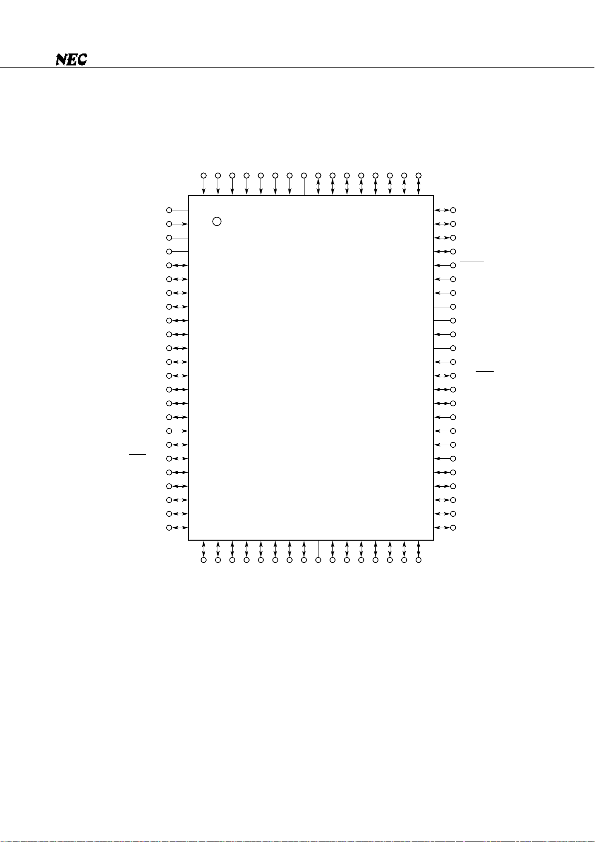
FUNCTIONS
ROM
RAM
24448 × 8 bits
1024 × 4 bits
(4-bit × 8 or 8-bit × 4) × 4 banks
• 0.67 µs/1.33 µs/2.67 µs/10.7 µs (At 6.0 MHz)
• 0.95 µs/1.91 µs/3.82 µs/15.3 µs (At 4.19 MHz)
• 122 µs (At 32.768 kHz)
64
16 (Shared with INT, SIO, PPO, and analog input. Seven lines can be pulled
up by software.)
28 (Four lines for LED driving)
• 16 lines can be pulled up by software.
• Four lines can be pulled down by the mask option.
20 (Eight lines for LED driving. Withstand voltage is 10 V. 20 lines can be
pulled up by the mask option.)
8-bit resolution × 8 channels (Successive approximation system)
• Capable of low-voltage operation: VDD = 2.7 to 6.0 V
Four channels • Timer/event counter
• Basic interval timer
• Timer/pulse generator (14-bit PWM output enabled)
• Clock timer
Two channels • NEC standard serial bus interface (SBI)/
three-wire SIO: One channel
• General clock synchronous serial interface
(three-wire SIO): One channel
• Vectored interrupt : Seven sources (External: 3, internal: 4)
• Test input : Two sources (External: 1, internal: 1)
• Clock test flag is provided.
• Parallel edge detection flag for key scan input is provided.
• Set/reset/test/Boolean operation for bit data
• 4-bit data transfer, arithmetic/logical, increment/decrement, and comparison
instructions
• 8-bit data transfer, arithmetic/logical, increment/decrement, and comparison
instructions
• Ceramic/crystal oscillator for main system clock : 6.0 MHz, 4.19 MHz
• Crystal oscillator for subsystem clock : 32.768 kHz
VDD = 2.7 to 6.0 V
80-pin plastic QFP (14 × 20 mm)
Built-in memory
General registers
Instruction cycle
I/O ports
A/D converter
Timer/counter
Serial interface
Interrupt
Instruction set
System clock generator
Operating supply voltage
Package
Item
Functions
Total
Number of CMOS
input lines
Number of CMOS
I/O lines
Number of N-ch
open-drain I/O lines
3
µ
PD75517(A)
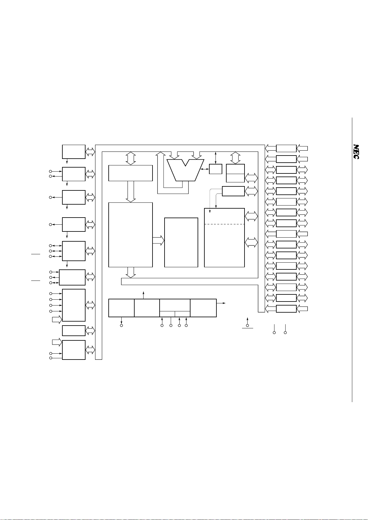
PIN CONFIGURATION (TOP VIEW)
IC: Internally connected. Connect the IC pin to VSS.
Note Be sure to supply power to both the VDD pins.
AN1
AN2
AN3
AN4/P150
AN5/P151
AN6/P152
AN7/P153
AV
SS
P120
P121
P122
P123
P130
P131
P132
P133
P140
P141
P142
P143
RESET
X2
X1
IC
XT2
XT1
V
SS
P00/INT4
P01/SCK0
P02/SO0/SB0
P03/SI0/SB1
P10/INT0
P11/INT1
P12/INT2
P13/TI0
P20/PTO0
P21
P22/PCL
P23/BUZ
P30
1
2
3
4
5
6
7
8
9
10
11
12
13
14
15
16
17
18
19
20
21
22
23
24
64
63
62
61
60
59
58
57
56
55
54
53
52
51
50
49
48
47
46
45
44
43
42
41
80 79 78 77 76 75 74 73 72 71 70 69 68 67 66 65
25 26 27 28 29 30 31 32 33 34 35 36 37 38 39 40
AN0
AV
REF
V
DD
V
DD
P113
P112
P111
P110
P103
P102
P101
P100
P93
P92
P91
P90
SI1/P83
SO1/P82
SCK1/P81
PPO/P80
KR7/P73
KR6/P72
KR5/P71
KR4/P70
KR3/P63
KR2/P62
KR1/P61
KR0/P60
P53
P52
P51
P50
V
SS
P43
P42
P41
P40
P33
P32
P31
Note
PD75517GF(A)-×××-3B9
µ
4
µ
PD75517(A)
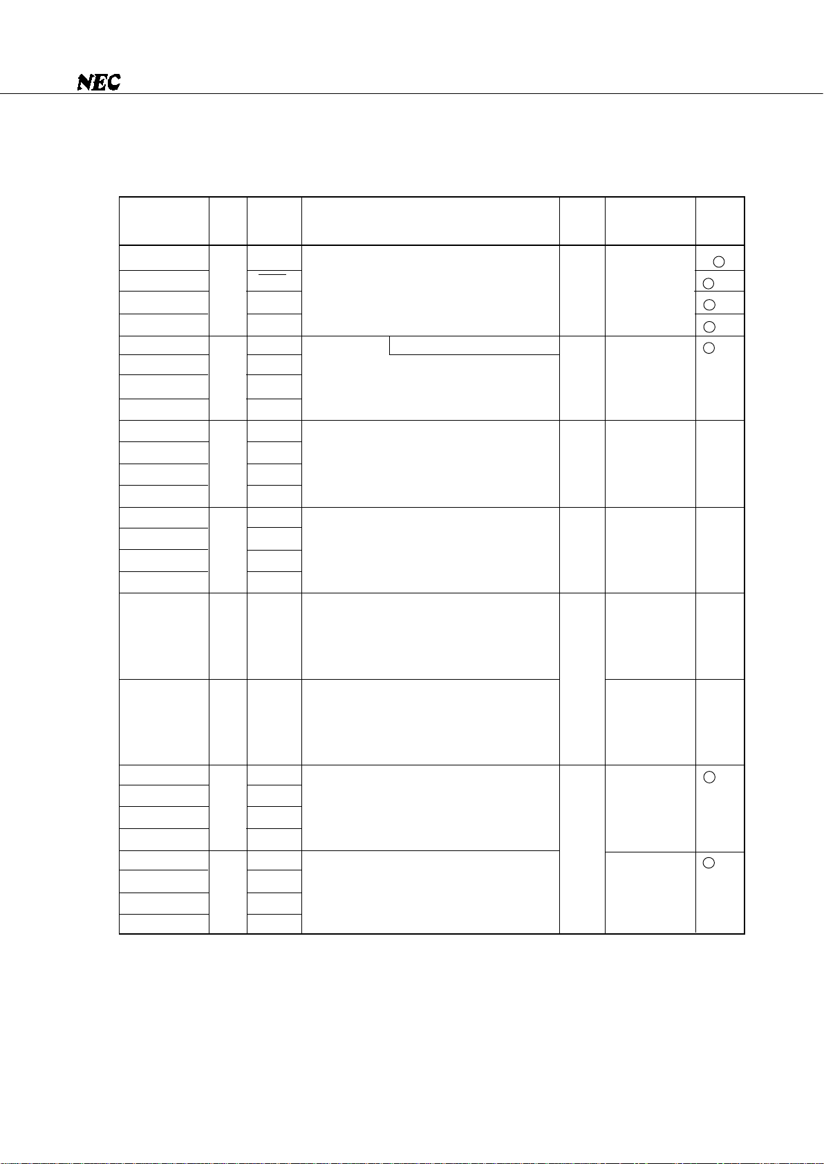
INTERNAL BLOCK DIAGRAM
TI0/P13
PTO0/P20
BUZ/P23
PPO/P80
SI0/SB1/P03
SO0/SB0/P02
SCK0/P01
SI1/P83
SO1/P82
SCK1/P81
INT0/P10
INT1/P11
INT2/P12
INT4/P00
KR0/P60
- KR7/P73
AN0 - AN3
AN4/P150
- AN7/P153
AV
REF
AVSS
P00 - P03
P10 - P13
P20 - P23
P30 - P33
P40 - P43
Note
P50 - P53
Note
P60 - P63
P70 - P73
P80 - P83
P90 - P93
P100 - P103
P110 - P113
P120 - P123
Note
P130 - P133
Note
P140 - P143
Note
P150 - P153
4
4
4
4
4
4
4
4
4
4
4
4
4
4
4
4
Port 0
Port 1
Port 2
Port 3
Port 4
Port 5
Port 6
Port 7
Port 8
Port 9
Port 10
Port 11
Port 12
Port 13
Port 14
Port 15
Basic
interval
timer
INTBT
Timer/event
counter #0
INTT0
Watch timer
INTW
Timer/pulse
generator
INTTPG
Serial bus
interface 0
INTCSI0
Serial
interface 1
Interrupt
control
Bit seq.
buffer (16)
A/D
converter
Program counter (15)
ROM program memory
24448 × 8 bits
ALU
CY
SP(8)
SBS(2)
Bank
Decode and
control
General register
RAM data memory
1024 × 4 bits
f
X/2
N
Clock output
control
PCL/P22
Clock divider
Clock generator
Sub Main
Stand by
control
XT1 XT2 X1 X2
CPU clock
Φ
RESET
VDD VSS
Note Port 4, Port 5, Port 12, Port 13, and Port 14 are N-ch open-drain
I/O ports with a medium withstand voltage of 10 V.

5
µ
PD75517(A)
CONTENTS
1. PIN FUNCTIONS ........................................................................................................................ 7
1.1 PORT PINS ...................................................................................................................................... 7
1.2 NON-PORT PINS ............................................................................................................................ 9
1.3 PIN INPUT/OUTPUT CIRCUITS .................................................................................................... 10
1.4 CONNECTION OF UNUSED PINS ................................................................................................ 13
1.5 SELECTION OF A MASK OPTION ................................................................................................ 14
2. ARCHITECTURE AND MEMORY MAP OF THE µPD75517(A) .............................................. 15
2.1 DATA MEMORY BANK CONFIGURATION AND ADDRESSING MODES ................................ 15
2.2 GENERAL REGISTER BANK CONFIGURATION .......................................................................... 19
2.3 MEMORY-MAPPED I/O ................................................................................................................. 22
3. INTERNAL CPU FUNCTIONS.................................................................................................... 27
3.1 PROGRAM COUNTER (PC) ........................................................................................................... 27
3.2 PROGRAM MEMORY (ROM) ........................................................................................................ 27
3.3 DATA MEMORY (RAM) ................................................................................................................. 29
3.4 GENERAL REGISTERS ................................................................................................................... 31
3.5 ACCUMULATORS .......................................................................................................................... 32
3.6 STACK POINTER (SP) AND STACK BANK SELECT REGISTER (SBS) ..................................... 32
3.7 PROGRAM STATUS WORD (PSW) .............................................................................................. 35
3.8 BANK SELECT REGISTER (BS) ..................................................................................................... 38
4. PERIPHERAL HARDWARE FUNCTIONS .................................................................................. 39
4.1 DIGITAL I/O PORTS ....................................................................................................................... 39
4.2 CLOCK GENERATOR ...................................................................................................................... 51
4.3 CLOCK OUTPUT CIRCUIT ............................................................................................................. 60
4.4 BASIC INTERVAL TIMER ............................................................................................................... 63
4.5 CLOCK TIMER ................................................................................................................................. 67
4.6 TIMER/EVENT COUNTER ............................................................................................................. 69
4.7 TIMER/PULSE GENERATOR ......................................................................................................... 75
4.8 SERIAL INTERFACE (CHANNEL 0) ............................................................................................... 83
4.8.1 Serial Interface (Channel 0) Functions........................................................................ 84
4.8.2 Configuration of Serial Interface (Channel 0) ............................................................ 84
4.8.3 Register Functions ......................................................................................................... 86
4.8.4 Signals ............................................................................................................................. 94
4.8.5 Serial Interface (Channel 0) Operation ....................................................................... 100
4.8.6 Transfer Start in Each Mode ........................................................................................ 110
4.8.7 Manipulation of SCK0 Pin Output ............................................................................... 111

6
µ
PD75517(A)
4.9 SERIAL INTERFACE (CHANNEL 1) ............................................................................................... 112
4.9.1 Serial Interface (Channel 1) Functions........................................................................ 112
4.9.2 Serial Interface (Channel 1) Configuration................................................................. 112
4.9.3 Register Functions ......................................................................................................... 114
4.9.4 Serial Interface (Channel 1) Operation ....................................................................... 115
4.10 A/D CONVERTER ........................................................................................................................... 117
4.11 BIT SEQUENTIAL BUFFER ............................................................................................................ 124
5. INTERRUPT FUNCTION ............................................................................................................ 125
5.1 CONFIGURATION OF THE INTERRUPT CONTROL CIRCUIT .................................................... 125
5.2 HARDWARE OF THE INTERRUPT CONTROL CIRCUIT .............................................................. 127
5.3 INTERRUPT SEQUENCE ................................................................................................................ 134
5.4 MULTIPLE INTERRUPT PROCESSING CONTROL ...................................................................... 135
5.5 VECTOR ADDRESS SHARE INTERRUPT PROCESSING ............................................................ 137
6. STANDBY FUNCTION ............................................................................................................... 138
6.1 SETTING OF STANDBY MODES AND OPERATION STATUSES ............................................. 138
6.2 RELEASE OF THE STANDBY MODES ......................................................................................... 139
6.3 OPERATION AFTER A STANDBY MODE IS RELEASED ............................................................ 141
7. RESET FUNCTION ..................................................................................................................... 142
8. INSTRUCTION SET .................................................................................................................... 144
8.1
µ
PD75517(A) INSTRUCTIONS ...................................................................................................... 144
8.2 INSTRUCTION SET AND ITS OPERATION .................................................................................. 147
8.3 INSTRUCTION CODES OF EACH INSTRUCTION ....................................................................... 156
9. ELECTRICAL CHARACTERISTICS............................................................................................. 162
10. PACKAGE DIMENSIONS ........................................................................................................... 174
11. RECOMMENDED SOLDERING CONDITIONS ......................................................................... 175
APPENDIX A SERIES PRODUCT FUNCTIONS ............................................................................ 176
APPENDIX B DEVELOPMENT TOOLS......................................................................................... 177
7
µ
PD75517(A)
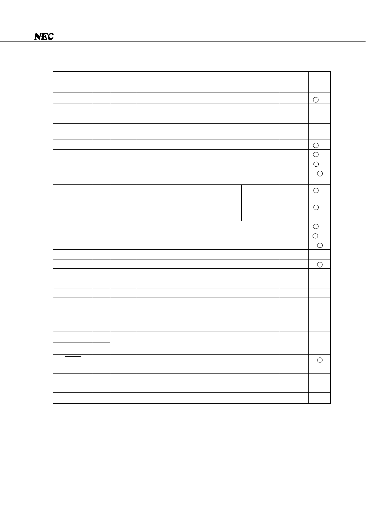
1. PIN FUNCTIONS
1.1 PORT PINS (1/2)
Notes 1. The circuits enclosed in circles have a Schmitt-triggered input.
2. An LED can be driven directly.
P00
P01
P02
P03
P10
P11
P12
P13
P20
P21
P22
P23
P30
Note 2
P31
Note 2
P32
Note 2
P33
Note 2
P40-P43
Note 2
P50-P53
Note 2
P60
P61
P62
P63
P70
P71
P72
P73
INT4
SCK0
SO0/SB0
SI0/SB1
INT0
INT1
INT2
TI0
PTO0
–
PCL
BUZ
–
–
–
–
–
–
KR0
KR1
KR2
KR3
KR4
KR5
KR6
KR7
×
×
×
×
❍
❍
With noise elimination function
4-bit input port (Port 0).
For P01 to P03, pull-up resistors can be
provided by software in units of 3 bits.
4-bit input port (Port 1).
Pull-up resistors can be provided by software
in units of 4 bits.
4-bit I/O port (Port 2).
Pull-up resistors can be provided by software
in units of 4 bits.
Programmable 4-bit I/O port (Port 3).
Input/output can be specified bit by bit.
Pull-up resistors can be provided by software
in units of 4 bits.
N-ch open-drain 4-bit I/O port (Port 4).
A pull-up resistor can be provided bit by bit
(mask option).
Withstand voltage is 10 V in open-drain mode.
N-ch open-drain 4-bit I/O port (Port 5).
A pull-up resistor can be provided bit by bit
(mask option).
Withstand voltage is 10 V in open-drain mode.
Programmable 4-bit I/O port (Port 6).
Input/output can be specified bit by bit.
Pull-up resistors can be provided by software
in units of 4 bits.
4-bit I/O port (Port 7).
Pull-up resistors can be provided by software
in units of 4 bits.
Also
used as
Pin name
I/O
B
F - A
F - B
M - C
B - C
E - B
E - C
M
M
F - C
F - A
8-bit I/O
Input
Input
Input
Input
High level
(when a pull-up
resistor is
provided) or
high impedance
High level
(when a pull-up
resistor is
provided) or
high impedance
Input
Input
When resetFunction
I
I
I/O
I/O
I/O
I/O
I/O
I/O
I/O
Note 1
circuit
type

8
µ
PD75517(A)
1.1 PORT PINS (2/2)
Note The circuits enclosed in circles have a Schmitt-triggered input.
×
×
×
×
×
×
×
Function
Also
used as
Pin name
I/O 8-bit I/O
When reset
I/O
Note
circuit
type
Input
Low level (when
a pull-down
resistor is
provided) or
high impedance
Input
Input
High level
(when a pull-up
resistor is
provided) or
high impedance
High level
(when a pull-up
resistor is
provided) or
high impedance
High level
(when a pull-up
resistor is
provided) or
high impedance
Input
PPO
SCK1
SO1
SI1
–
–
–
–
–
–
AN4-AN7
I
I/O
I/O
I/O
I/O
I/O
I/O
I
P80
P81
P82
P83
P90-P93
P100-P103
P110-P113
P120-P123
P130-P133
P140-P143
P150-P153
E
F
E
B
V
E
E
M
M
M
Y - A
4-bit input port (Port 8).
4-bit I/O port (Port 9).
A pull-down resistor can be provided bit by bit
(mask option).
4-bit I/O port (Port 10)
4-bit I/O port (Port 11)
N-ch open-drain, 4-bit I/O port (Port 12).
Pull-up resistors can be provided bit by bit
(mask option).
Withstand voltage is 10 V in open-drain mode.
N-ch open-drain, 4-bit I/O port (Port 13).
Pull-up resistors can be provided bit by bit
(mask option).
Withstand voltage is 10 V in open-drain mode.
N-ch open-drain, 4-bit I/O port (Port 14).
Pull-up resistors can be provided bit by bit
(mask option).
Withstand voltage is 10 V in open-drain mode.
4-bit input port (Port 15)
9
µ
PD75517(A)
1.2 NON-PORT PINS
Notes 1. The circuits enclosed in circles have a Schmitt-triggered input.
2. Be sure to input V
SS level to this pin.
Function
Also
used as
Pin name
I/O
I
O
O
O
I/O
I/O
I/O
I
I
I
I
I
I/O
O
I
I
I
–
I
I
–
I
O
–
–
–
Synchronous
Asynchronous
Asynchronous
Edge detection vectored interrupt input pin
(The edge to be detected is selectable.)
Edge detection testable input pin
(An rising edge is detected.)
P13
P20
P22
P23
P01
P02
P03
P00
P10
P11
P12
P60-P63
P70-P73
P81
P82
P83
–
P150-P153
–
–
–
–
–
P80
–
–
–
External event pulse input pin for the timer/event counter
Timer/event counter output pin
Clock output pin
Fixed frequency output pin (for buzzer or system clock
trimming)
Serial clock I/O pin
Serial data output pin or serial bus I/O pin
Serial data input pin or serial bus I/O pin
Edge detection vectored interrupt input pin (Either a rising
or falling edge is detected.)
Parallel-falling-edge-sensitive testable input pins
Parallel-falling-edge-sensitive testable input pins
Serial clock I/O pin
Serial data output pin
Serial data input pin
Analog input pins to A/D converter
A/D converter reference voltage input pin
A/D converter reference GND pin
Pin for connection to a crystal/ceramic resonator for main
system clock generation. When external clock is used, it is
input to X1, and its inverted signal is input to X2.
Pin for connection to a crystal resonator for subsystem
clock generation. When external clock is used, it is input to
XT1, and XT2 is left open.
System reset input pin
Timer/pulse generator pulse output pin
Positive power supply pin
Ground pin
Internally connected
Note 2
–
Input
Input
Input
Input
Input
Input
–
–
–
Input
Input
Input
Input
Input
–
–
–
–
–
–
Input
–
–
–
TI0
PTO0
PCL
BUZ
SCK0
SO0/SB0
SI0/SB1
INT4
INT0
INT1
INT2
KR0-KR3
KR4-KR7
SCK1
SO1
SI1
AN0-AN3
AN4-AN7
AVREF
AVSS
X1, X2
XT1
XT2
RESET
PPO
VDD
VSS
IC
I/O
Note 1
circuit
type
When reset
B - C
E - B
E - B
E - B
F - A
F - B
M - C
B
B - C
B - C
F - C
F - A
F
E
B
Y
Y - A
Z
–
–
–
B
E
–
–
–
10
µ
PD75517(A)
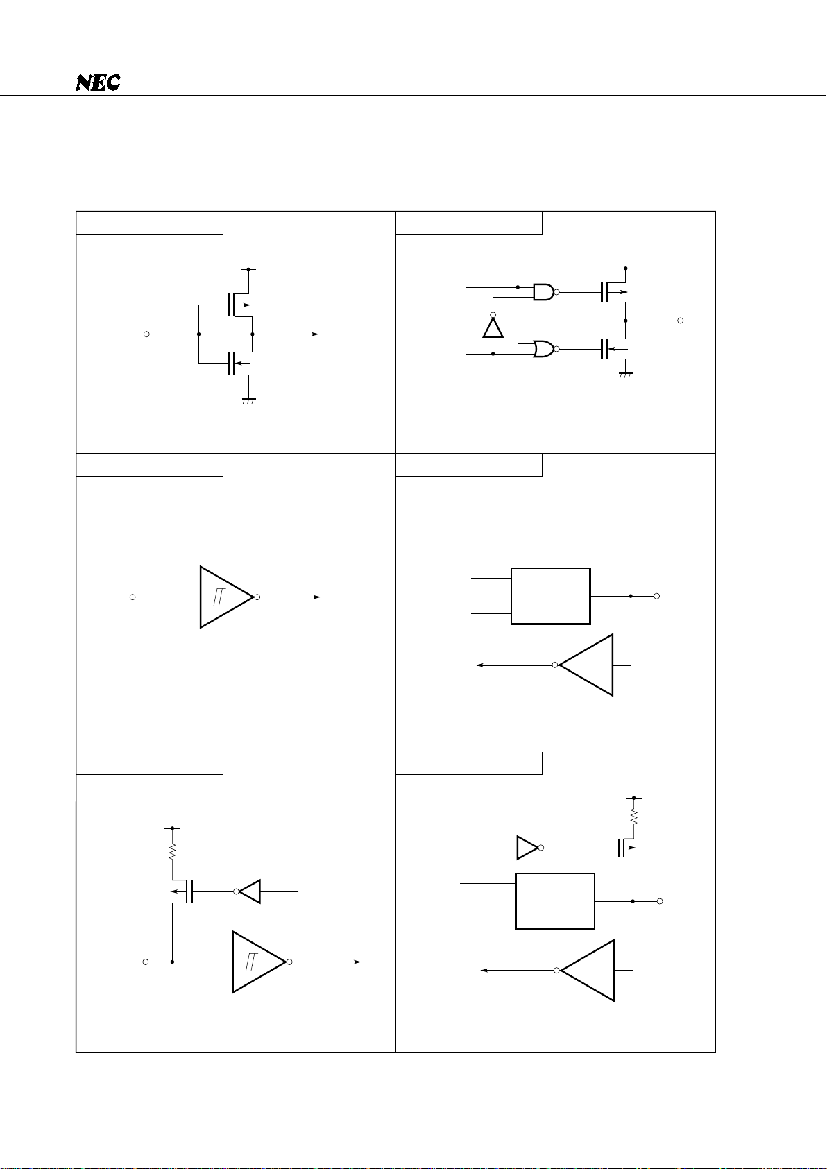
1.3 PIN INPUT/OUTPUT CIRCUITS
Fig. 1-1 shows the input/output circuit of each
µ
PD75517(A) pin in a simplified manner.
Fig. 1-1 Pin Input/Output Circuits (1/3)
Type A
CMOS input buffer
Schmitt trigger input with hysteresis
Push-pull output which can be set to high-impedance output
(off for both P-ch and N-ch)
I/O circuit consisting of a push-pull output
of type D and an input buffer of type A
P.U.R.: Pull-Up Resistor
Type B Type E
Type B - C
Type D
VDD
IN
P-ch
N-ch
IN
IN
P-ch
P.U.R.
enable
P.U.R.
V
DD
VDD
P-ch
N-ch
OUT
Data
Output
disable
IN/OUT
Data
Output
disable
Type D
Schmitt trigger input with hysteresis
P.U.R.: Pull-Up Resistor
P.U.R.
V
DD
Output
disable
P-ch
IN/OUT
Data
Output
disable
Type D
Type E - B
Type A
Type A
11
µ
PD75517(A)
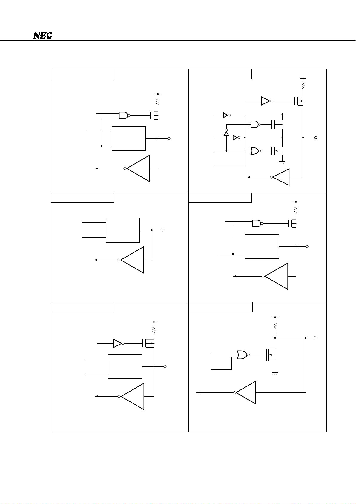
Fig. 1-1 Pin Input/Output Circuits (2/3)
Type E - C
I/O circuit consisting of a push-pull output of type D
and a Schmitt-triggered input of type B
P.U.R.: Pull-Up Resistor
Type F
Type F - A
Type F - B
P.U.R.
V
DD
P.U.R.
enable
P-ch
IN/OUT
Data
Output
disable
Type D
IN/OUT
Data
Output
disable
Type D
P.U.R.: Pull-Up Resistor
P.U.R.
V
DD
P.U.R.
enable
P-ch
IN/OUT
Data
Output
disable
Type D
P.U.R.: Pull-Up Resistor
VDD
P-ch
N-ch
IN/OUT
VDD
P-ch
P.U.R.
P.U.R.
enable
Output
disable
(P-ch)
Data
Output
disable
Output
disable
(N-ch)
Type F - C
P.U.R.: Pull-Up Resistor
P.U.R.
V
DD
P.U.R.
enable
P-ch
IN/OUT
Data
Output
disable
Type D
Type M
P.U.R.: Pull-Up Resistor
N-ch
(Can sustain
+9 V)
IN/OUT
Data
VDD
Output
disable
P.U.R.
(Mask option)
Middle-voltage input buffer
(Can sustain + 10 V)
Type B
Type A
Type B
Type B
Type B
12
µ
PD75517(A)
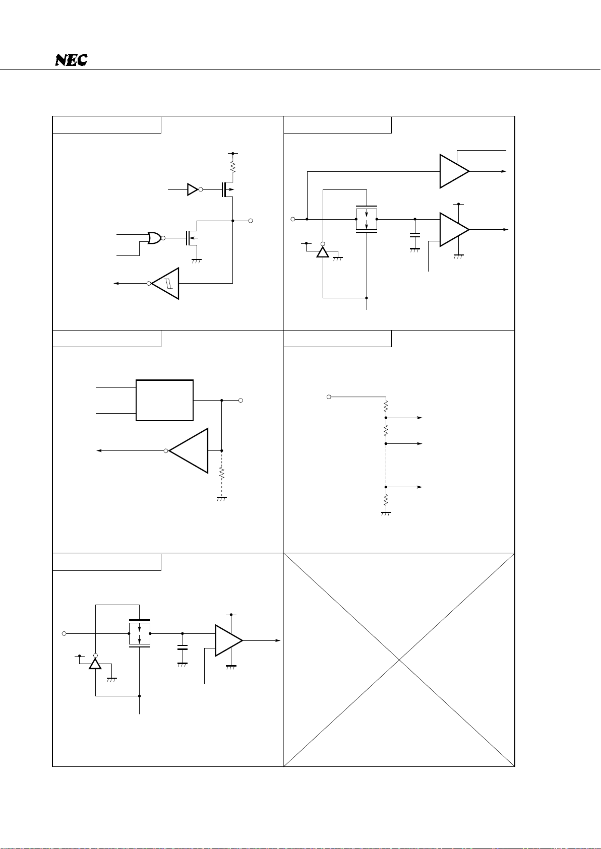
Fig. 1-1 Pin Input/Output Circuits (3/3)
Type V
Type M - C
Type Y
Type Z
Type Y - A
P.D.R.: Pull-Down Resistor
P.U.R.: Pull-Up Resistor
P.D.R.
(Mask option)
IN/OUT
Data
Output
disable
Type D
N-ch
P.U.R.
Data
Output
disable
P.U.R.
enable
V
DD
P-ch
IN/OUT
V
DD
V
DD
P-ch
AV
SS
N-ch
Sampl-
ing C
AV
SS
Reference voltage
(from voltage tap of
serial resistor string)
Input
enable
IN
V
DD
AV
SS
Sampl-
ing C
V
DD
AV
SS
IN
P-ch
N-ch
Reference voltage
(from voltage tap of
serial resistor string)
IN instruction
+
–
Input
enable
AV
REF
Reference voltage
AV
SS
+
–
Type A

13
µ
PD75517(A)
1.4 CONNECTION OF UNUSED PINS
Table 1-1 Recommended Connection of Unused Pins
To be connected to VSS
To be connected to VSS or VDD
To be connected to VSS
Input state : To be connected to VSS or VDD
Output state : To be left open
To be connected to VSS or VDD
Input state : To be connected to VSS or VDD
Output state : To be left open
To be connected to VSS
To be connected to VSS or VDD
To be left open
To be connected to VSS
P00/INT4
P01/SCK0
P02/SO0/SB0
P03/SI1/SB1
P10/INT0-P12/INT2
P13/TI0
P20/PTO0
P21
P22/PCL
P23/BUZ
P30-P33
P40-P43
P50-P53
P60/KR0-P63/KR3
P70/KR4-P73/KR7
P80/PPO
P81/SCK1
P82/SO1
P83/SI1
P90-P93
P100-P103
P110-P113
P120-P123
P130-P133
P140-P143
P150/AN4-P153/AN7
AN0-AN3
XT1
XT2
AVREF
AVSS
IC
Pin name Recommended connection
14
µ
PD75517(A)
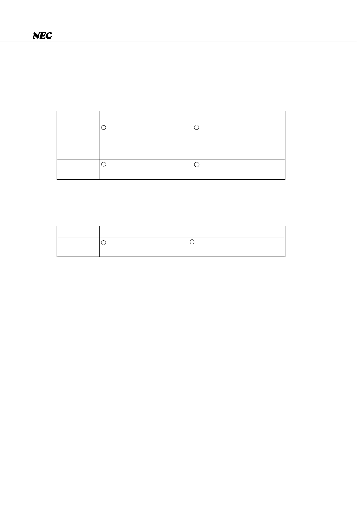
1.5 SELECTION OF A MASK OPTION
The following mask options are provided for pins.
(1) Specification of built-in pull-up and pull-down resistors
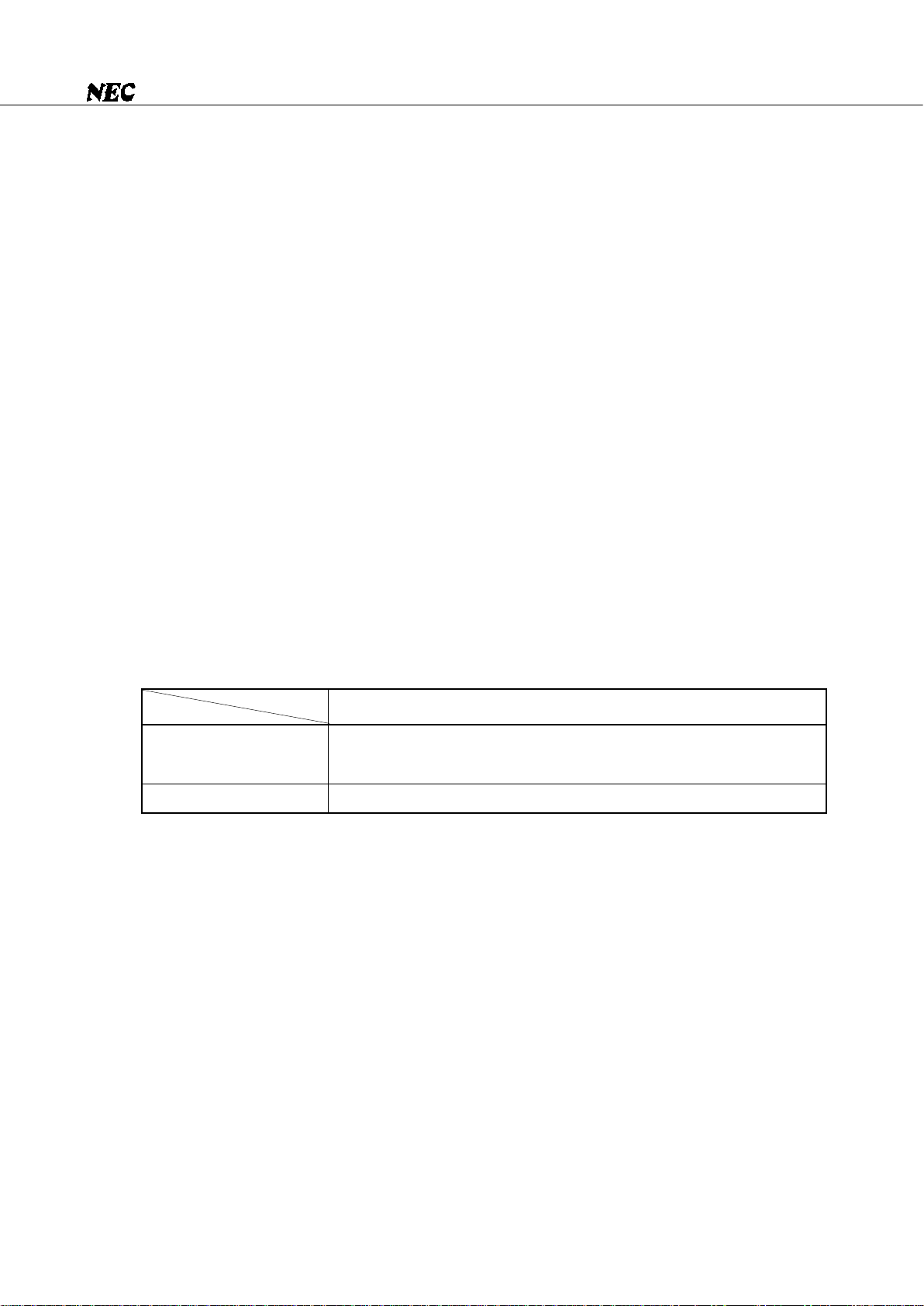
Table 1-2 Selection of Pull-Up and Pull-Down Resistors
(2) Specification of built-in feed-back resistors for subsystem clock oscillation
Table 1-3 Selection of Feed-Back Resistors
Caution Even if built-in feed-back resistors are provided when no subsystem clock is used, operation is
not affected except increased power supply current I
DD.
P40-P43,
P50-P53,
P120-P123,
P130-P133,
P140-P143
P90-P93
Pin name
2 No pull-up resistor provided
(Can be specified bit by bit.)
2 No pull-down resistor provided
(Can be specified bit by bit.)
1 Pull-up resistors provided
(Can be specified bit by bit.)
1 Pull-down resistors provided
(Can be specified bit by bit.)
Mask option
XT1, XT2 1 Feed-back resistors provided
(when a subsystem clock is used)
2 No feed-back resistors provided
(when no subsystem clock is used)
Mask optionPin name
15
µ
PD75517(A)
2. ARCHITECTURE AND MEMORY MAP OF THE µPD75517(A)
The µPD75517(A) has three architectural features:
(a) Data memory bank configuration
(b) General register bank configuration
(c) Memory-mapped I/O
Each of these features is explained below.
2.1 DATA MEMORY BANK CONFIGURATION AND ADDRESSING MODES
As shown in Fig. 2-1, the data memory space of the
µ
PD75517(A) contains a static RAM (1024 words × 4
bits) at addresses 000H to 3FFH and peripheral hardware (such as I/O ports and timers) at addresses F80H to
FFFH. To address a 12-bit address in this data memory space, the µPD75517(A) uses such a memory bank
configuration that the low-order eight bits are specified with an instruction directly or indirectly, and the highorder four bits are used to specify a memory bank (MB).
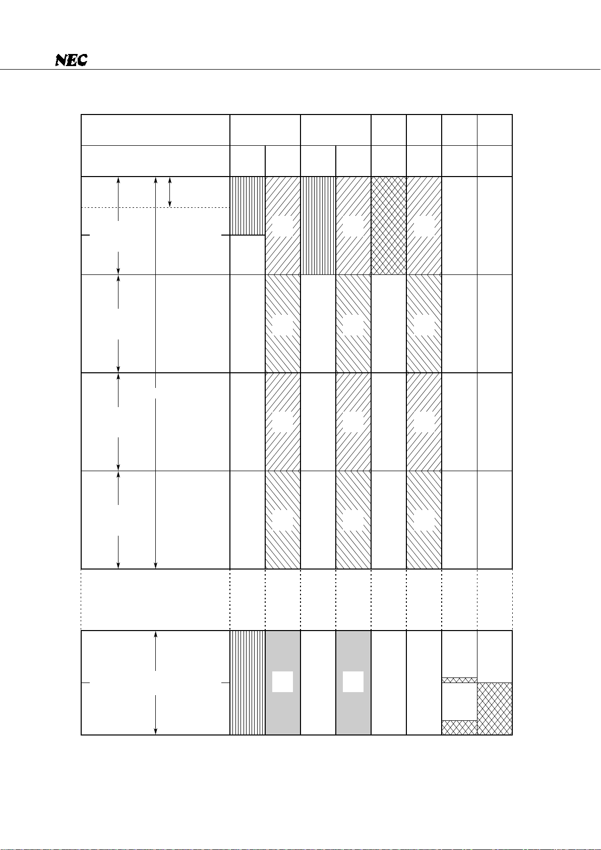
To specify a memory bank (MB), a memory bank enable flag (MBE) and memory bank select register (MBS)
are contained, allowing the addressing indicated in Fig. 2-1 and 2-2 and Table 2-1. (The MBS is a register used
to select a memory bank, and can be set to 0, 1, 2, 3, or 15. The MBE is a flag used to determine whether a
memory bank selected using the MBS register is to be enabled. The MBE is automatically saved or restored
at the time of interrupt processing or subroutine processing, so that it can be freely set in interrupt processing
and subroutine processing.)
In addressing data memory space, the MBE is usually set to 1 (MBE = 1), and the static RAM in the memory
bank specified by the MBS is operated. However, the MBE = 0 mode or the MBE = 1 mode can be selected
for each step of program processing for more efficient programming.
The MBE and MBS are set as indicated below.
Example SET1 MBE ; MBE ← 1
CLR1 MBE ; MBE ← 0
SEL MB0 ; MBS ← 0
SEL MB1 ; MBS ← 1
SEL MB15 ; MBS ← 15
• Interrupt processing
• Processing that repeats internal hardware and static RAM operations
• Subroutine processing
• Usual program processing
MBE = 0 mode
MBE = 1 mode
Applicable program processing
16
µ
PD75517(A)
Fig. 2-1 Data Memory Organization and Addressing Range of Each Addressing Mode
Remark — : Don’t care
FF0H
FFFH
FB0H
FBFH
FC0H
F80H
3FFH
2FFH
300H
1FFH
200H
0FFH
100H
01FH
020H
07FH
000H
Addressing mode
mem
mem.bit
@HL
@H + mem.bit
@DE
@DL
Stack
address-
ing
fmem.bit
pmem.
@L
Memory bank enable flag
MBE
= 0
MBE
= 1
MBE
= 0
MBE
= 1
––– –
Data area
Static RAM
(memory bank 0)
Data area
Static RAM
(memory bank 1)
Data area
Static RAM
(memory bank 2)
Data area
Static RAM
(memory bank 3)
Stack area
Not contained
Peripheral hardware area
(memory bank 15)
MBS
= 0
MBS
= 0
SBS
= 0
MBS
= 1
MBS
= 1
SBS
= 1
MBS
= 2
MBS
= 2
SBS
= 2
MBS
= 3
MBS
= 3
SBS
= 3
MBS
= 15
MBS
= 15
General
resister
area

17
µ
PD75517(A)
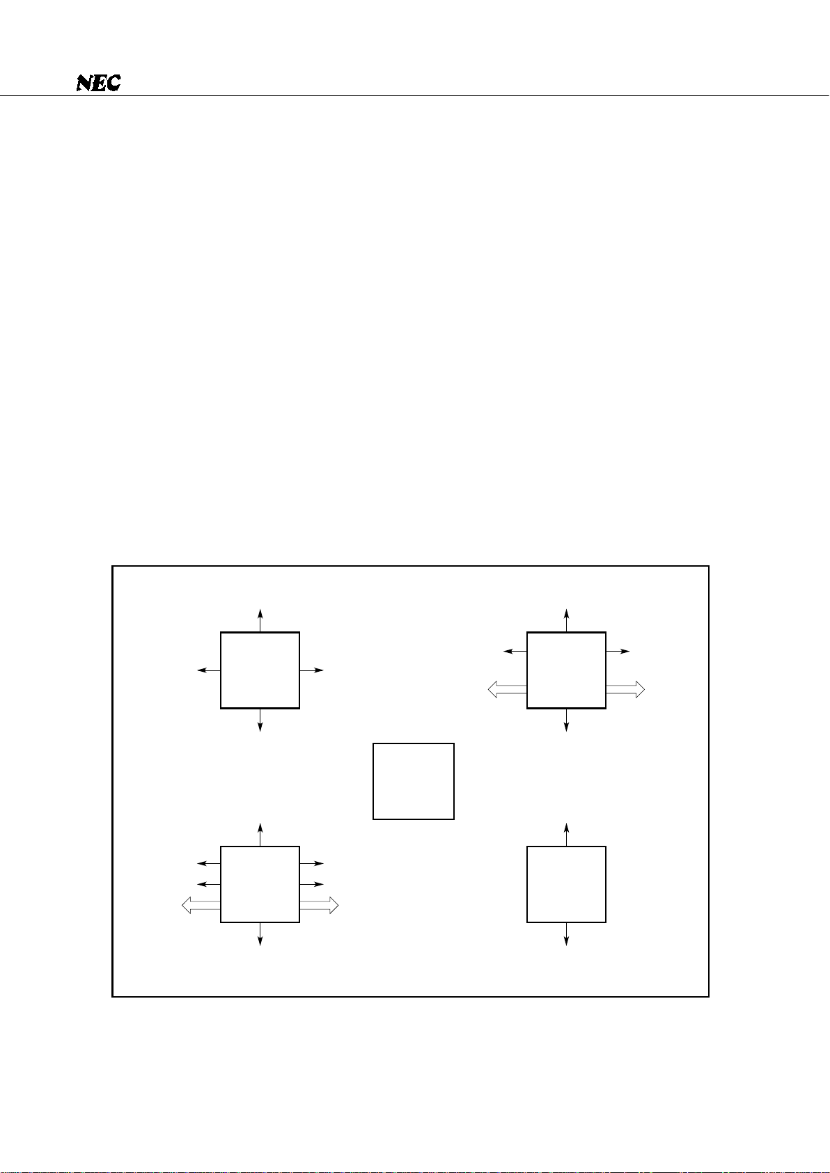
Table 2-1 Addressing Modes
Bit specified by bit at the address specified by MB and mem. In this case:
When MBE = 0 and mem = 00H-7FH, MB = 0
When MBE = 0 and mem = 80H-FFH, MB = 15
When MBE = 1, MB = MBS
Address specified by MB and mem. In this case:
When MBE = 0 and mem = 00H-7FH, MB = 0
When MBE = 0 and mem = 80H-FFH, MB = 15
When MBE = 1, MB = MBS
Address specified by MB and mem (mem: even address). In this case:
When MBE = 0 and mem = 00H-7FH, MB = 0
When MBE = 0 and mem = 80H-FFH, MB = 15
When MBE = 1, MB = MBS
Address specified by MB and HL.
In this case, MB = MBE•MBS
Address specified by DE in memory bank 0
Address specified by DL in memory bank 0
Address specified by MB and HL (with the L register holding an even number).
In this case, MB = MBE•MBS
Bit specified by bit at the address specified by fmem. In this case:
fmem = FB0H-FBFH (interrupt-related hardware)
fmem = FF0H-FFFH (I/O port)
Bit specified by the low-order 2 bits of the L register at the address specified
by the high-order 10 bits of pmem and the high-order 2 bits of the L register.
In this case, pmem = FC0H-FFFH
Bit specified by bit at the address specified by MB, H, and the low-order 4 bits
of mem.
In this case, MB = MBE•MBS
Address specified by SP in memory bank 0, 1, 2, and 3 selected by SBS
1-bit direct addressing
4-bit direct addressing
8-bit direct addressing
4-bit register indirect
addressing
8-bit register indirect
addressing
Bit manipulation
addressing
Stack addressing
mem.bit
mem
@HL
@HL+
@HL–
@DE
@DL
@HL
fmem.bit
pmem.@L
@H+mem.bit
—
Representation
format
Specified addressAddressing mode
18
µ
PD75517(A)
As summarized in Table 2-1, the µPD75517(A) allows both direct and indirect addressing in data memory
manipulation for 1-bit data, 4-bit data, and 8-bit data, so that very efficient and simple programming can be
performed.
Examples 1. The 8-bit data of port 4 and port 5 are transferred to addresses 20H and 21H.
CLR1 MBE ; MBE ← 0
IN XA, PORT4 ; XA ← Ports 5, 4
MOV 20H, XA ; (21H, 20H) ← XA
2. When P02 is 0, P33 is set.
SKT PORT0.2 ; Skip if bit 2 of port 0 is 1
SET1 PORT3.3 ; Set bit 3 of port 3
3. A different value is output to port 6, depending on the status of P10.
SKF PORT1.0 ; Skip if bit 0 of port 1 is 0
MOV A, #1010B ; A ← 1010B (string effect)
MOV A, #0101B ; A ← 0101B (string effect)
SEL MB15 ; or CLR1 MBE
OUT PORT6, A ; Port 6 ← A
Fig. 2-2 Updating Static RAM Addresses
INCS D
DECS D
INCS LDECS L
INCS D
DECS D
INCS EDECS E
INCS H
DECS H
INCS LDECS L
INCS H
DECS H
× 0H
0 × H
F × H
@DL
4-bit transfer
@DE
4-bit transfer
@HL
4-bit
manipulation
8-bit
manipulation
@H + mem.bit
Bit manipulation
Direct
addressing
Bit manipulation
4-bit
8-bit
× FH
DECS DE INCS DE
DECS HL INCS HL
Automatic
decrement
Automatic
increment

19
µ
PD75517(A)
2.2 GENERAL REGISTER BANK CONFIGURATION
The
µ
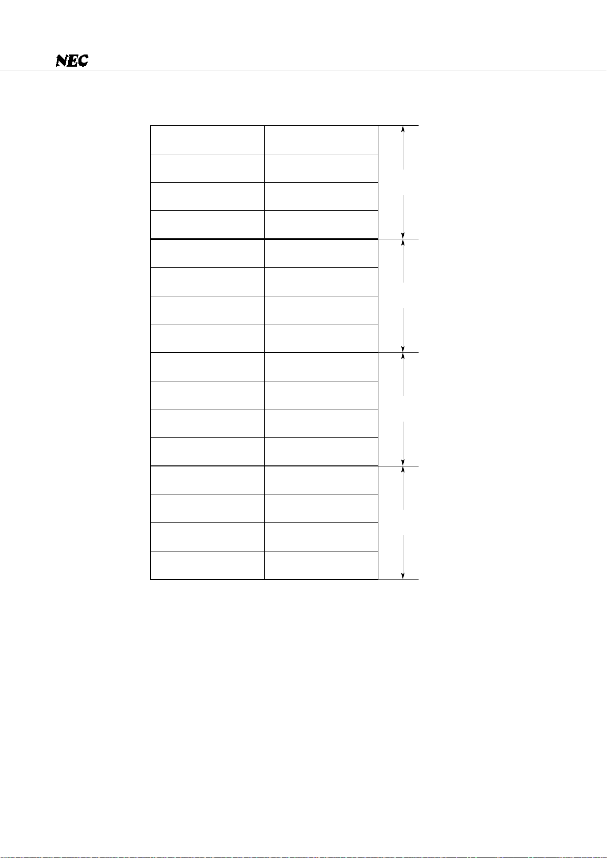
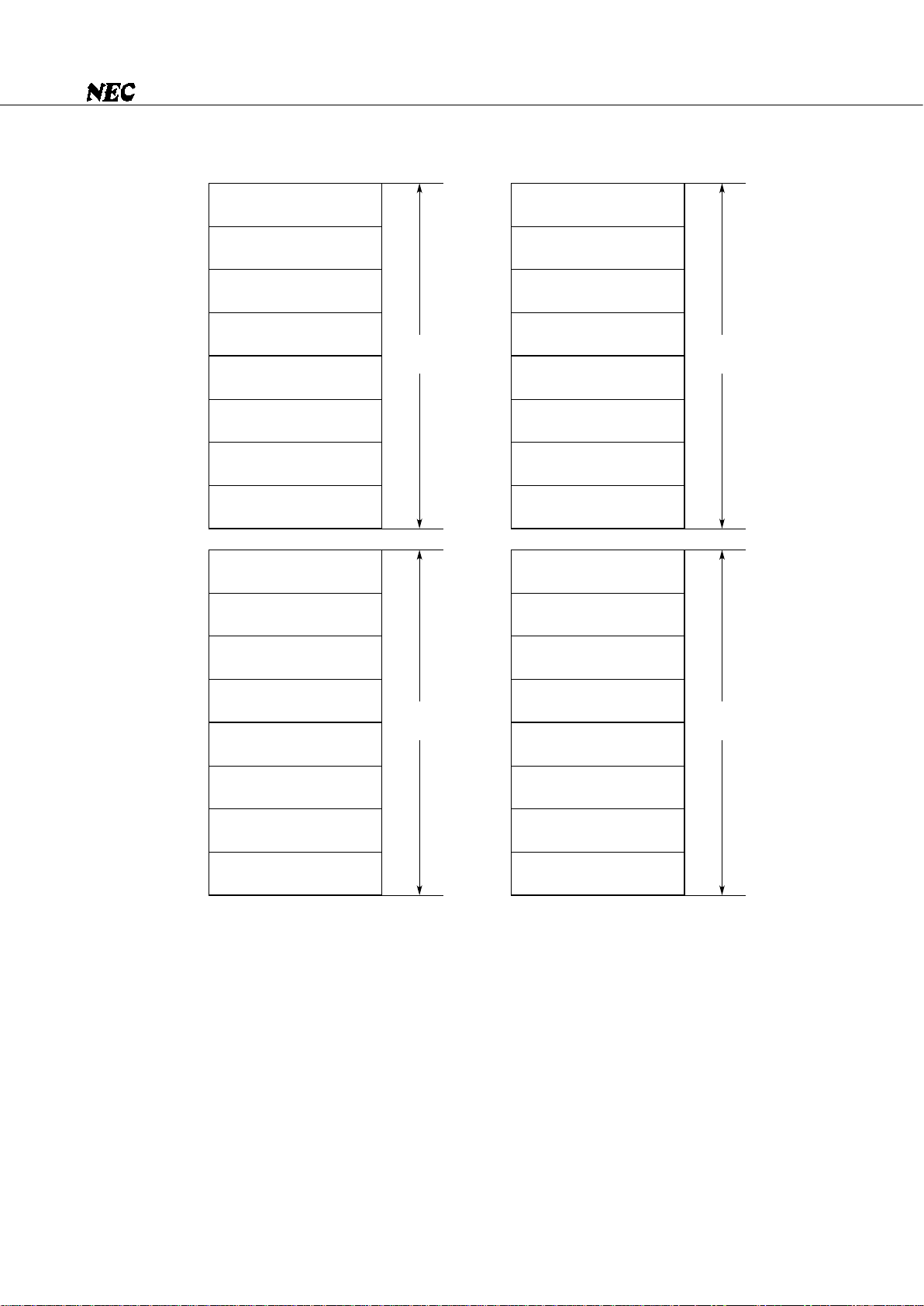
PD75517(A) contains four register banks, each consisting of eight general registers: X, A, B, C, D, E,
H, and L. These registers are mapped to addresses 00H to 1FH in memory bank 0 of the data memory. (See
Fig. 2-3.) To specify a general register bank, a register bank enable flag (RBE) and a register bank select register
(RBS) are contained. The RBS is a register used to select a register bank, and the RBE is a flag used to determine
whether a register bank selected using the RBS is to be enabled. The register bank (RB) enabled at instruction
execution is determined as RB = RBE•RBS
As indicated in Table 2-2, the
µ
PD75517(A) enables the user to create programs in a very efficient manner
by selecting a register bank from the four register banks, depending on whether the processing is normal
processing or interrupt processing. (The RBE is automatically saved and set at the time of interrupt processing,
and is automatically restored upon completion of interrupt processing.)
Table 2-2 Example of the Use of Register Banks with Normal Routines and Interrupt Routines
The RBE and RBS are set as indicated below.
Example SET1 RBE ; RBE ← 1
CLR1 RBE ; RBE ← 0
SEL RB0 ; RBS ← 0
SEL RB3 ; RBS ← 3
The general registers allow transfers, comparisons, arithmetic/logical operations, and increments and
decrements not only on a 4-bit basis, but also on an 8-bit basis with the XA, HL, DE, and BC register pairs.
In this case, the register pairs of the register bank that has the inverted value of bit 0 of a register bank specified
by RBE•RBS can be specified as XA’, HL’, DE’, and BC’, thus providing eight 8-bit registers. (See Fig. 2-4.)
Example SET1 RBE ; RBE ← 1
SEL RB2 ; RBS ← 2
MOV XA, #18H ; XA ← 18H
ADDS HL, XA ; HL ← HL+XA
SUBS HL’, XA ; HL’ ← HL’–XA (HL’ is HL of register bank 3)
INCS HL ; HL ← HL+1
MOV XA, #00H ; XA ← 00H (string effect)
MOV XA, #10H ; XA ← 10H (string effect)
Normal processing
Single interrupt processing
Dual interrupt processing
Multiple (triple or more) interrupt processing
Use register banks 2 and 3 with RBE = 1.
Use register bank 0 with RBE = 0.
Use register bank 1 with RBE = 1.
(In this case, the RBS needs to be saved and restored.)
Save the registers with PUSH or POP.
20
µ
PD75517(A)
Fig. 2-3 General Register Configuration (4-Bit Processing)
X
H
D
B
X
H
D
B
X
H
D
B
X
H
D
B
01H
03H
05H
07H
09H
0BH
0DH
0FH
11H
13H
15H
17H
19H
1BH
1DH
1FH
A
L
E
C
A
L
E
C
A
L
E
C
A
L
E
C
00H
02H
04H
06H
08H
0AH
0CH
0EH
10H
12H
14H
16H
18H
1AH
1CH
1EH
Register bank 0
(RBE·RBS = 0)
Register bank 1
(RBE·RBS = 1)
Register bank 2
(RBE·RBS = 2)
Register bank 3
(RBE·RBS = 3)
21
µ
PD75517(A)
Fig. 2-4 General Register Configuration (8-Bit Processing)
XA
HL
DE
BC
XA’
HL’
DE’
BC’
00H
02H
04H
06H
08H
0AH
0CH
0EH
When RBE·RBS
= 0
XA’
HL’
DE’
BC’
XA
HL
DE
BC
00H
02H
04H
06H
08H
0AH
0CH
0EH
When RBE·RBS
= 1
XA
HL
DE
BC
XA’
HL’
DE’
BC’
10H
12H
14H
16H
18H
1AH
1CH
1EH
When RBE·RBS
= 2
XA’
HL’
DE’
BC’
XA
HL
DE
BC
10H
12H
14H
16H
18H
1AH
1CH
1EH
When RBE·RBS
= 3

22
µ
PD75517(A)
2.3 MEMORY-MAPPED I/O
The
µ
PD75517(A) employs memory-mapped I/O, which maps peripheral hardware such as timers and I/O
ports to addresses F80H to FFFH in the data memory space as shown in Fig. 2-1. This means that there is no
particular instruction to control peripheral hardware, but all peripheral hardware is controlled using memory
manipulation instructions. (Some mnemonics for hardware control are available to make programs readable.)
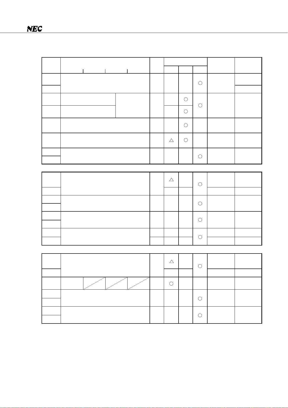
To manipulate peripheral hardware, the addressing modes listed in Table 2-3 can be used.
Table 2-3 Addressing Modes Applicable to Peripheral Hardware
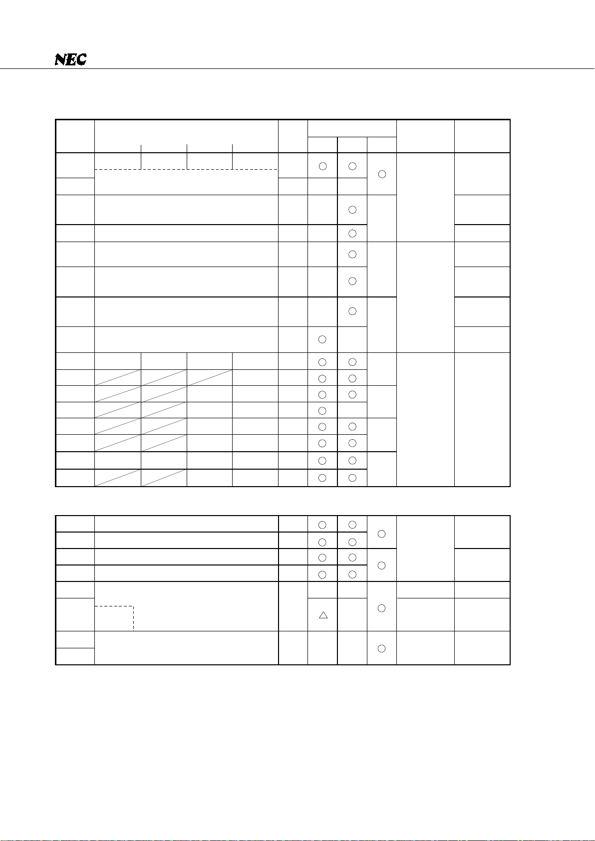
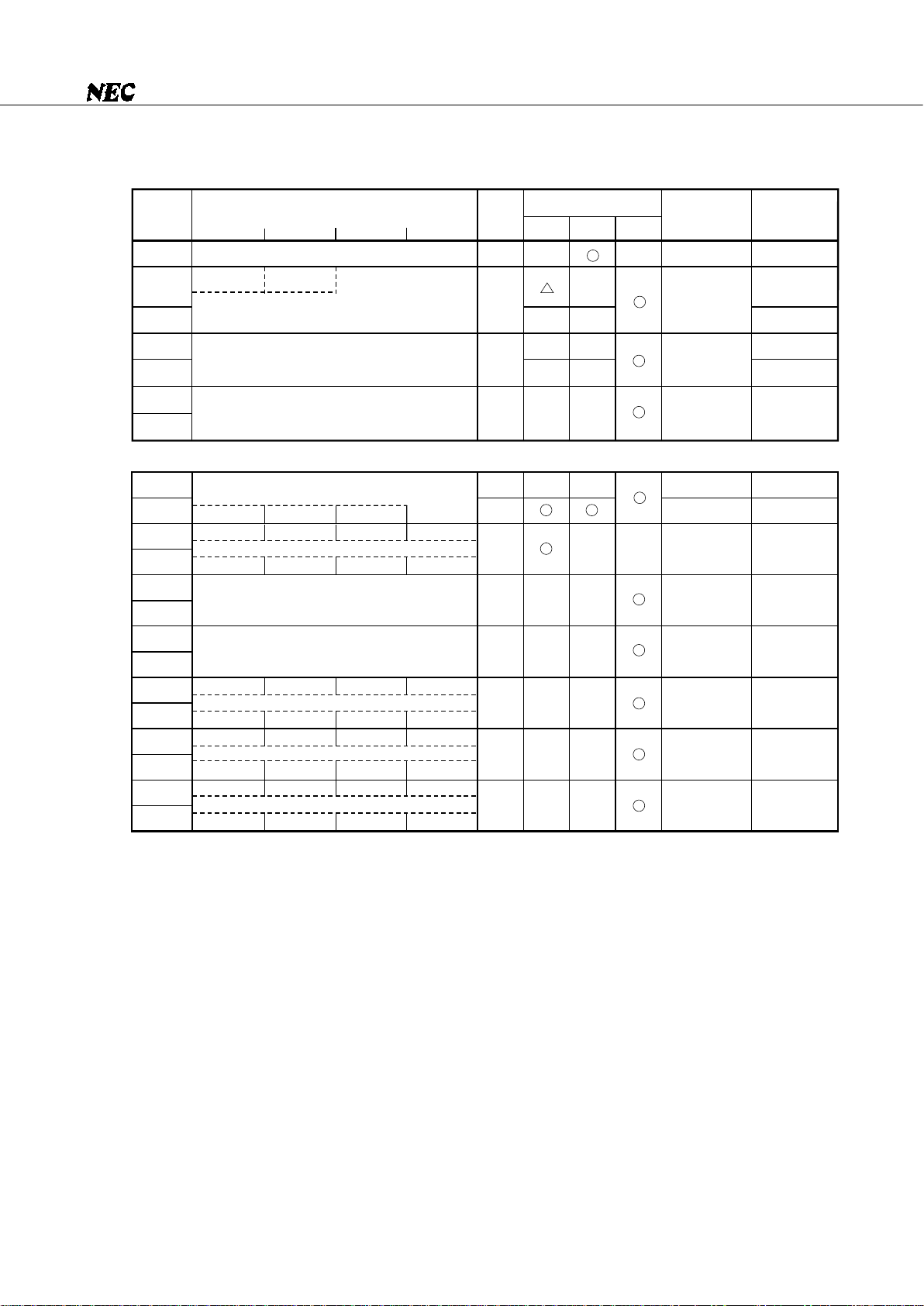
Fig. 2-5 summarizes the I/O map of the
µ
PD75517(A).
The items in Fig. 2-5 have the following meanings:
• Symbol: Name representing the address of incorporated hardware, which can be coded in the operand
field of an instruction
• R/W : Indicates whether the hardware allows read/write operation.
R/W: Both read and write operations possible
R : Read only
W : Write only
• Number of manipulatable bits:
Indicates the number of bits that can be processed in hardware manipulation
: Bits can be manipulated on an indicated bit (1-, 4-, or 8-bit) basis.
: Particular bits can be manipulated. For these bits, see Remarks.
: Bits cannot be manipulated on an indicated bit (1-, 4-, or 8-bit) basis.
• Bit manipulation addressing:
Bit manipulation addressing applicable in hardware bit manipulation
Bit manipulation
4-bit manipulation
8-bit manipulation
Direct addressing mode specifying mem.bit with MBE = 0 or
(MBE = 1, MBS = 15)
Direct addressing mode specifying fmem.bit regardless of MBE
and MBS setting
Indirect addressing mode specifying pmem.@L regardless of
MBE and MBS setting
Direct addressing mode specifying mem with MBE = 0 or (MBE
= 1, MBS = 15)
Register indirect addressing mode specifying @HL with (MBE
= 1, MBS = 15)
Direct addressing mode specifying mem (even address) with
MBE = 0 or (MBE = 1, MBS = 15)
Register indirect addressing mode specifying @HL (with the L
register containing an even number) with (MBE = 1, MBS = 15)
All hardware allowing bit
manipulation
IST0, IST1, MBE, RBE, EOT,
IE×××, IRQ×××, PORTn.×
BSBn.×
PORTn.×
All hardware allowing 4-bit
manipulation
All hardware allowing 8-bit
manipulation addressing
Applicable addressing mode
Applicable hardware
–
23
µ
PD75517(A)
Fig. 2-5 µPD75517(A) I/O Map (1/4)
Notes 1. Can be operated separately as the RBS and MBS during 4-bit manipulation.
Can also be operated as the BS during 8-bit manipulation.
2. TOE0: Timer/event counter 0 output enable flag (W)
R/W – –
W
–
R/W
Address
b0b1b2b3
F80H
F85H
F86H
F98H
FA0H
FA2H
FA4H
FA6H
TOE0
Note 2
R
W
W
W
R
W
––
–
––
–
––
––
––
––
–
mem.bit
mem.bit
mem.bit
Remarks
Bit
manipulation
addressing
Bit 0 is fixed
to 0
Hardware name (symbol)
Number of bits that
Stack pointer (SP)
Basic interval timer mode register (BTM)
Basic interval timer (BT)
Clock mode register (WM)
Timer/event counter 0 mode register (TM0)
Timer/event counter 0 count register (T0)
Timer/event counter 0 modulo register (TMOD0)
Only bit 3
allows bit
manipulation.
Only bit 3 can
be manipulat-
ed
1 bit 4 bits 8 bits
F82H
F83H
F84H
Register bank select register
(RBS)
Memory bank select register
(MBS)
Bank select
register (BS)
Stack bank select register (SBS) R/W
Bits 3 and 2
are always
set to 0.
R
Note 1
–
–
––
F90H
F94H
Timer pulse generator (TPGM)
mem.bit
Only bit 3 can
be manipulat-
ed
–
W
––
F96H
Timer/pulse generator modulo register (MODL)
R/W
––
Timer/pulse generator modulo register (MODH) R/W
––
–
can be manipulated
24
µ
PD75517(A)
Fig. 2-5 µPD75517(A) I/O Map (2/4)
Remarks 1. IE××× : Interrupt enable flag
2. IRQ×××: Interrupt request flag
R/W
–
R/WAddress
b0b1b2b3
FB0H
FB2H
FB3H
FC0H
FC2H
FC3H
fmem.bit
mem.bit
pmem.@L
RBEMBEIST0IST1
––
R
–
–
–
–
–
–
W
W
W
W
W
–
–
R/W
–
R/W
R/W
R/W
–
R/W
–
R/W
fmem.bit
FB4H
FB5H
FB6H
FB7H
FB8H
FBAH
FBCH
FBDH
FBEH
FBFH
IE4 IRQ4 IEBT IRQBT
IEW IRQW
IET0 IRQT0
IECSI0 IRQCSI0
IE0 IRQ0
IE2 IRQ2
IE1 IRQ1
R/W
R/W
R/W
R/W
FC1H
Remarks
Bit
manipulation
addressing
Hardware name (symbol)
1 bit 4 bits 8 bits
Program status word (PSW)
Processor clock control register (PCC)
INT0 mode register (IM0)
INT1 mode resistor (IM1)
INT2 mode register (IM2)
System clock control register (SCC)
Bit sequential buffer 0 (BSB0)
Bit sequential buffer 1 (BSB1)
Bit sequential buffer 2 (BSB2)
Bit sequential buffer 3 (BSB3)
Manipulated
with EI/DI
instruction
Bit 2 is fixed
to 0
Bits 3, 2, and
1 are fixed to
0
Bits 3 and 2
are fixed to
0
Bits 2 and 1
are fixed to 0
–
Interrupt priority select register (IPS)
W
FBBH
IETPG IRQTPG
FB9H
EOT R/W
R/W
–
FC8H
Serial operation mode register 1 (CSIM1)
Only bit 7
allows bit
manipulation.
FCCH
Serial I/O shift register 1 (SIO1)
CSIE1
W
R/W
––
–
––
mem.bit
Number of bits that
can be manipulated
25
µ
PD75517(A)
Fig. 2-5 µPD75517(A) I/O Map (3/4)
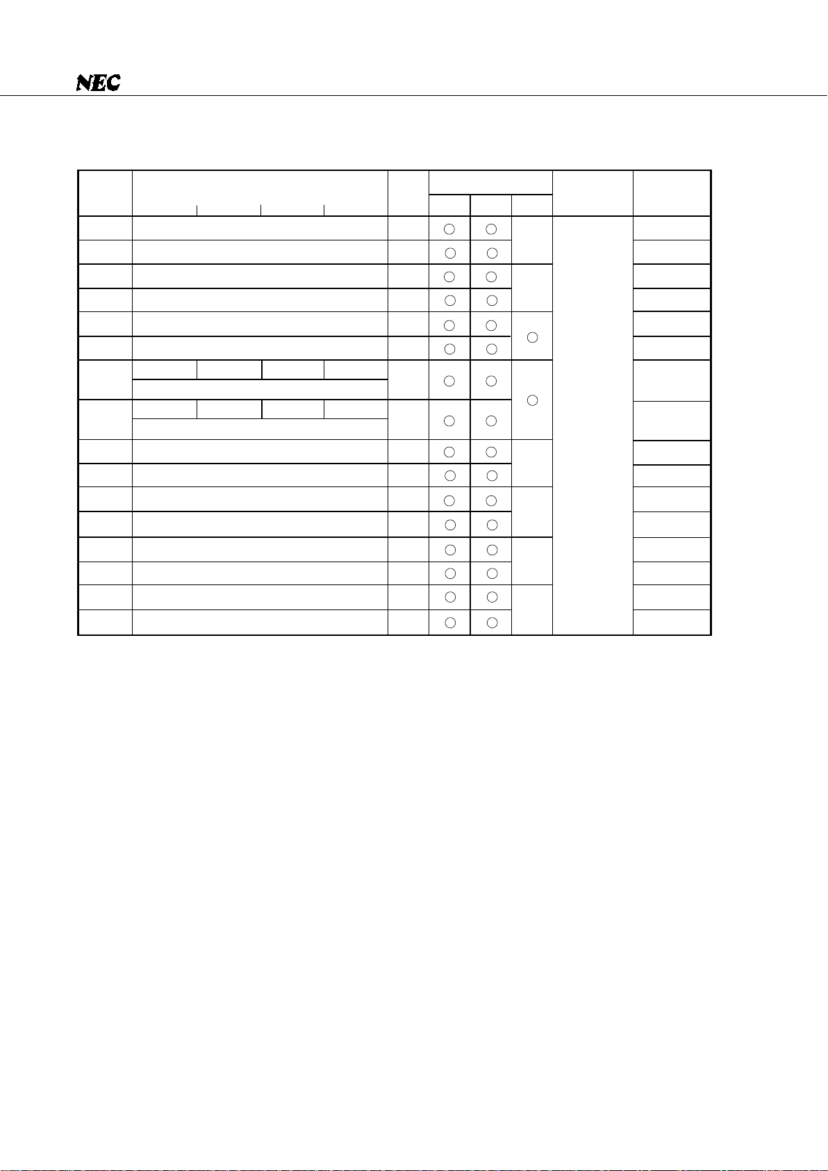
Note When developing a program, set 0 to the following two bits of the port mode register group C (PMGC):
FEEH, b0 (Equivalent to PM8)
FEFH, b3 (Equivalent to PM15)
For, while this port on the chip side is used for input only, the corresponding port on the emulator
is an I/O port.
W
R/WAddress
b0b1b2b3
FD0H
FD8H
FDAH
–
–
––
W
–
–
R
W
FDCH
EOCSOC
–
–
–
b3: 1-bit write
b2: 1-bit read
W
R/W
FE0H
FE2H
FE4H
mem.bit
–
–
–
W
FE6H
–
–
R/W
––
mem.bit
FE8H
FEEH
–
W
–
–
W
–
PM32PM33 PM31 PM30
PM10
PM11
PM9 –
Note
PM62PM63 PM61 PM60
PM14
PM13 PM12
R/W
Remarks
Bit
manipulation
addressing
Hardware name (symbol)
1 bit 4 bits 8 bits
Clock output mode register (CLOM)
A/D conversion mode register (ADM)
SA register (SA)
Pull-up resistor specification register group A
(POGA)
Serial operation mode register 0 (CSIM0)
SBI control register (SBIC)
Serial I/O shift register 0 (SIO0)
Slave address register (SVA)
Port mode register group A (PMGA)
Port mode register group C (PMGC)
b6: 1-bit read
All bits allow
bit manipula-
tion only
–
––
COICSIE0 WUP
RELDCMDD CMDT RELT
ACKDBSYE
ACKE ACKT
FECH
–
W
–
PM2
–
––
–PM7
PM5 PM4
Port mode register group B (PMGB)
–
Note
Number of bits that
can be manipulated
26
µ
PD75517(A)
Fig. 2-5 µPD75517(A) I/O Map (4/4)
Note KR0 to KR7 are read-only. In 4-bit parallel input processing, PORT6 or PORT7 is specified.
R
R/WAddress
b0b1b2b3
FF0H
FF1H
FF3H
fmem.bit
pmem.@L
FF5H
R
–
KR2KR3 KR1 KR0
FF2H
FF4H
FF6H
Note
FFBH
R/W
R/W
R/W
R/W
R/W
R
–
–
Remerks
Bit
manipulation
addressing
Hardware name (symbol)
1 bit 4 bits 8 bits
Port 0 (PORT0)
Port 1 (PORT1)
Port 3 (PORT3)
Port 5 (PORT5)
Port 2 (PORT2)
Port 4 (PORT4)
Port 11 (PORT11)
Port 6 (PORT6)
KR6KR7 KR5 KR4
FF7H
Note
R/W
Port 7 (PORT7)
R/W
R/W
R/W
Port 9 (PORT9)
Port 8 (PORT8)
Port 10 (PORT10)
Port 15 (PORT15)
Port 13 (PORT13)
Port 12 (PORT12)
Port 14 (PORT14)
R
R/W
R/W
R/W
–
–
–
FFAH
FF9H
FF8H
FFCH
FFDH
FFEH
FFFH
Number of bits that
can be manipulated

27
µ
PD75517(A)
3. INTERNAL CPU FUNCTIONS
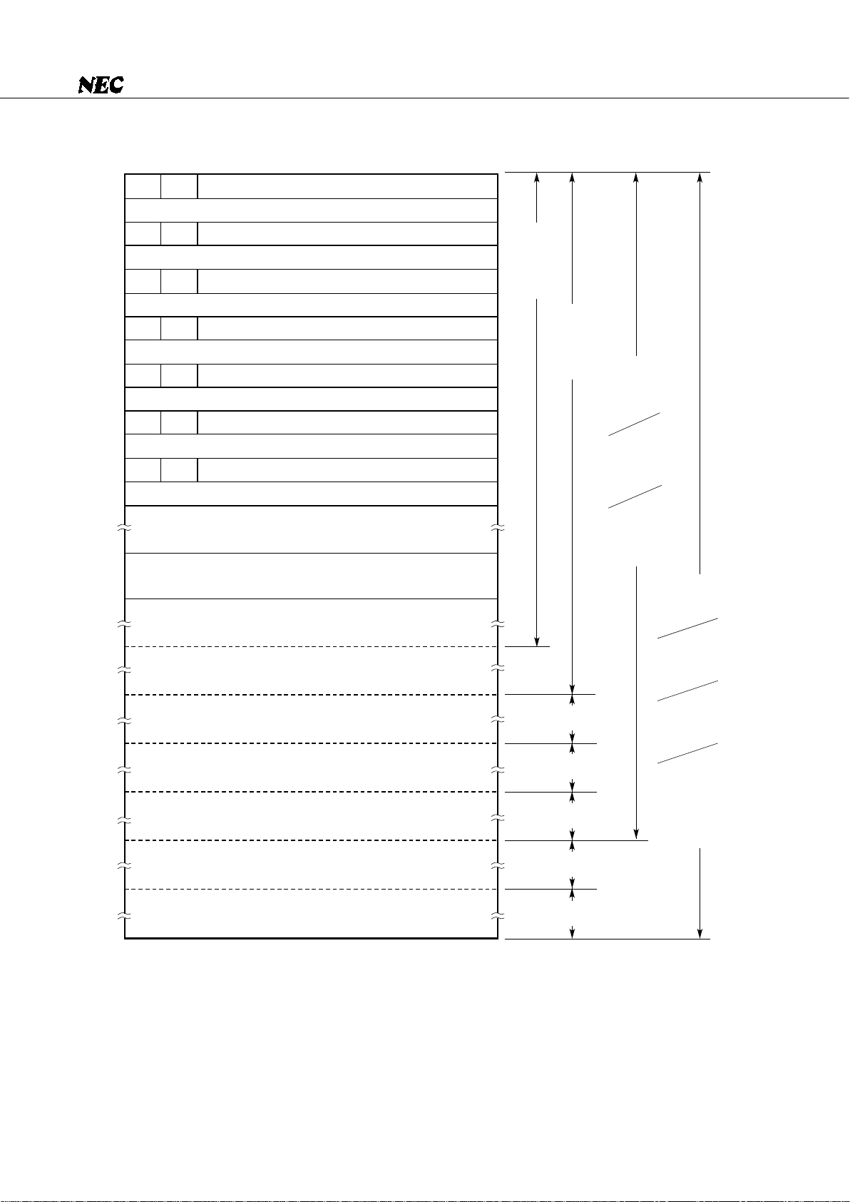
3.1 PROGRAM COUNTER (PC): 15 BITS
The program counter is a 15-bit binary counter for holding program memory address information.
Fig. 3-1 Program Counter Format
Note that the reset start address must be set within a space of 16K bytes (0000H to 3FFFH). This is because
a RESET input sets the low-order six bits of program memory address 0000H in PC13 to PC8, and the contents
of address 0001H in PC7 to PC0, and 0 in PC14 for initialization.
3.2 PROGRAM MEMORY (ROM): 24448 WORDS × 8 BITS
The program memory is a mask-programmable ROM with a configuration of 24448 words × 8 bits for storing
programs, table data, and so forth.
Program memory is addressed by the program counter. Table data can be referenced using the table
reference instruction (MOVT).
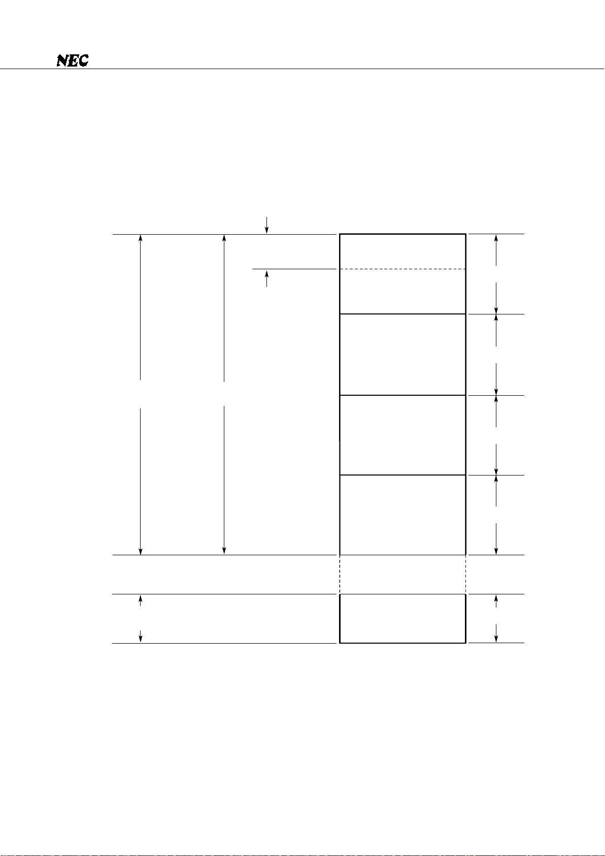
Fig. 3-2 shows the allowable branch address ranges for the branch instructions and subroutine call
instructions. The whole-space branch instruction (BRA !addr1) and the whole-space call instruction (CALLA
!addr1) allow a direct branch throughout the whole space 0000H-5F7FH. The relative branch instruction (BR
$addr) allows a branch to addresses (PC - 15 to PC - 1 and PC + 2 to PC + 16) regardless of block boundaries.
The program memory is located at addresses 0000H to 5F7FH containing the following specially assigned
addresses. (All areas excluding 0000H and 0001H can be used as normal program memory.)
• 0000H to 0001H
Vector table for holding the RBE and MBE setting values and program start address at the time of a RESET
input. A reset start can be performed at an arbitrary address within a 16K-byte space (0000H to 3FFFH).
• 0002H to 000DH
Vector table for holding the RBE and MBE setting values and program start address at the time of each
vectored interrupt occurrence. Interrupt processing can be started at an arbitrary address within a 16Kbyte space (0000H to 3FFFH).
• 0020H to 007FH
Table area referenced by the GETI instruction
Note
Note The GETI instruction can represent an arbitrary 2-byte or 3-byte instruction or two 1-byte instructions
in 1 byte, thus reducing the number of program steps. (See Section 8.1.)
PC12 PC11 PC10 PC9 PC8 PC7 PC6 PC5 PC4 PC3 PC2 PC1 PC0 PCPC13PC14
28
µ
PD75517(A)
Fig. 3-2 Program Memory Map
Caution The start address of an interrupt vector shown above consists of 14 bits. So, the start address
must be set within a 16K-byte space (0000H to 3FFFH).
Remark In addition to the above, the BR PCDE and BR PCXA instructions can cause a branch to an address
with only the low-order 8 bits of the PC changed.
MBE RBE
76
0000H
MBE RBE
0002H
MBE RBE0004H
MBE RBE0006H
MBE RBE0008H
MBE RBE000AH
007FH
0080H
0020H
0FFFH
1000H
2FFFH
3000H
5F7FH
0
Internal reset start address (high-order 6 bits)
Internal reset start address (low-order 8 bits)
INTBT/INT4 start address (high-order 6 bits)
INTBT/INT4 start address (low-order 8 bits)
INT0 start address (high-order 6 bits)
INT0 start address (low-order 8 bits)
INT1 start address (high-order 6 bits)
INT1 start address (low-order 8 bits)
INTCSI0 start address
(high-order 6 bits)
INTCSI0 start address
(low-order 8 bits)
INTT0 start address (high-order 6 bits)
INTT0 start address (low-order 8 bits)
INTTPG start address (high-order 6 bits)
INTTPG start address (low-order 8 bits)
GETI instruction reference table
BR !addr
instruction
branch
address
CALL !addr
instruction
branch
address
Branch/call
address specified
in GETI
insturction
CALLF
!faddr
instruction
entry
address
BRCB
!caddr
instruction
branch
address
MBE RBE000CH
BRCB !caddr instruction
branch address
BRCB !caddr instruction
branch address
BRCB !caddr instruction
branch address
BRCB !caddr instruction
branch address
BRCB !caddr instruction
branch address
5000H
4FFFH
4000H
3FFFH
2000H
1FFFH
07FFH
0800H
BR BCDE
BR BCXA
branch address
BRA !addr
instruction
branch address
CALLA !addr
instruction branch
address
BR $addr
instruction
relative
branch address
(–15 to –1,
+2 to +16)
29
µ
PD75517(A)
3.3 DATA MEMORY (RAM)
The data memory is divided into a data area and a peripheral hardware area as shown in Fig. 3-3.
The data memory consists of the following memory banks, with each bank made of 256 words × 4 bits:
• Memory banks 0, 1, 2, and 3 (data area)
• Memory bank 15 (peripheral hardware area)
Fig. 3-3 Data Memory Map
(32 × 4)
Data memory
000H
01FH
020H
2FFH
300H
3 FFH
F80H
FFFH
256 × 4
256 × 4
128 × 4
0
2
15
Stack
area
General
register
area
Data area
Static RAM
(1024 × 4)
Peripheral
hardware area
Not contained
256 × 4
256 × 4
1
3
0FFH
100H
1FFH
200H
Memory bank

30
µ
PD75517(A)
(1) Data area
The data area consists of a static RAM, and is used for storing data and as stack memory for subroutine
and interrupt execution. The memory can hold data even if CPU operation is stopped in the standby mode,
so that it is suitable for holding memory contents with a battery for a long time. The data area can be
manipulated with memory manipulation instructions.
The static RAM is mapped in memory banks 0, 1, 2, and 3, with each made up of 256 × 4 bits. Bank 0 is
used as a data area, but can also be used as a general register area (000H to 01FH).
Whole addresses of memory banks 0, 1, 2, and 3 (000H to 3FFH) can be used as a stack area.
The static RAM has a configuration of four bits per address. However, use of manipulation instructions
enables 1-, 4-, and 8-bit manipulation. Note that an even address must be specified in an 8-bit manipulation
instruction.
(a) General register area
The general register area can be manipulated with either general register manipulation instructions
or memory manipulation instructions. Up to 32 4-bit registers are available. Of the 32 general
registers, registers not used by the program can be used as a data area or stack area.
(b) Stack memory area
The stack area can be allocated within a bank with the stack pointer (SP). The bank for the stack area
is selected from the memory banks 0, 1, 2, and 3 with the stack bank select register (SBS). Stack area
can be used as a save area for subroutine or interrupt execution.
Use memory manipulation instructions to manipulate the stack bank select register (SBS) and the
stack pointer (SP).
(2) Peripheral hardware area
The peripheral hardware area is mapped at addresses F80H to FFFH of memory bank 15.
Memory manipulation instructions are used to manipulate the peripheral hardware area as well as the
static RAM area. Note that, however, the number of bits to be manipulated at a time varies according to
the individual addresses. Addresses to which no peripheral hardware is assigned cannot be accessed
since such address locations contain no data memory.
 Loading...