NEC UPD75512GF-XXX-3B9, UPD75512GF-A-XXX-3B9 Datasheet

The mark ★ shows major revised points.
DESCRIPTION
The µPD75512(A) is a 4-bit single-chip microcomputer which employs 75X series architecture, and its
performance is comparable to that of an 8-bit microcomputer.
In addition to its high-speed processing capabilities, the
µ
PD75512(A) is also capable of processing data in
units of 1, 4, or in 8-bits. With its internally provided A/D converter and serial interface, the
µ
PD75512(A) provides
the highest performance in its class.
Detailed functions are described in the following user‘s manual. Be sure to read it for designing.
µ
PD75516 User‘s Maual: IEM-5049
FEATURES
• Higher reliability than µPD75512
• Adequate I/O lines: 64
(can be provided with pull-up/pull-down resistors: 47)
• Built-in 8-bit serial interface: 2-ch
NEC standard serial bus interface (SBI) internally provided
• Built-in 8-bit A/D converter: 8-ch
• Variable instruction execution time function which is convenient for high-speed operation and power saving
· 0.95
µ
s/1.95 µs/15.3 µs (at 4.19 MHz operation),
· 122
µ
s (at 32.768 kHz operation)
• Program memory (ROM) size: 12,160 × 8 bits
• Data memory (RAM) size: 512 × 4 bits
• High-performance timer function: 4-ch
· 8-bit timer/event counter
· Watch timer
· 8-bit basic interval timer
· Timer/pulse generator: Capable of outputting 14-bit PWM
• Clock operation for reduced power consumption possible
(5
µ
A TYP. at 3 V operation)
• PROM version (
µ
PD75P516) available
APPLICATIONS
Switable for automotive and transportation equipments, etc.
NEC Corporation 1991
Document No. IC-2815A
(O. D. No. IC-8265A)
Date Published January 1994 P
Printed in Japan
DATA SHEET
MOS INTEGRATED CIRCUIT
µ
PD75512(A)
The information in this document is subject to change without notice.
4-BIT SINGLE-CHIP MICROCOMPUTER
µ
PD75512(A)
2
Electrical
Specifications
Item
Product
ORDERING INFORMATION
Part Number Package Quality Grade
µ
PD75512GF(A)-xxx-3B9 80-pin plastic QFP Special
(14 × 20mm)
Remarks: xxx is ROM code number.
Please refer to “Quality Grade on NEC Semiconductor Devices” (Document number IEI-1209) published by NEC
Corporation to know the specification of quality grade on the devices and its recommended applications.
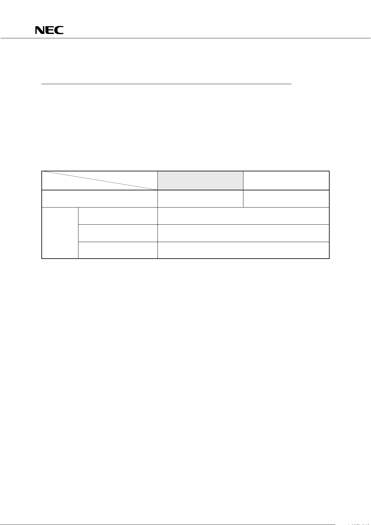
Difference between
µ
PD75512(A) and µPD75512
µ
PD75512(A)
µ
PD75512
Quality Grade Special Standard
Absolute Maximum Ratings Differ in high-level and low-level output current
DC Characteristics Differ in low-level output voltage
A/D Converter Characteristics Differ in ambient temperature range and absolute accuracy

µ
PD75512(A)
3
µ
PD75512(A) FUNCTIONS
Item Function
Internal ROM 12160 × 8 bits
Memory
Size RAM 512 × 4 bits
Genearl-Purpose Register (4 bits × 8 or 8 bits × 4) × 4 banks
Instruction Cycle • 0.95 µs/1.91 µs/15.3 µs (Main system clock: at 4.19 MHz)
• 122 µs (Subsystem clock: at 32.768 kHz)
Total 64 lines
CMOS Inputs 16 lines (also serve as INT, SIO, PPO, analog input; can be pulled up by software: 7
lines)
Input/
Output CMOS 28 lines
Ports Input/Outputs • Can be pulled up by software: 16 lines
• Can be pulled down by mask option: 4 lines
N-ch Open-Drain 20 lines (10 V withstand voltage; pins that can be pulled up by mask option: 20)
Input/Outputs
A/D Converter 8-bit resolution × 8 channels (successive approxmation type)
• Operation voltage: VDD = 3.5 to 6.0 V
• Timer/event counter
• Basic interval timer
• Timer/pulse generator (capable of outputting 14-bit PWM)
• Watch timer
• NEC standard serial bus interface (SBI)/3-line SIO: 1 channel
• Normal clock synchronized serial interface (3-line SIO): 1 channel
Vector Interrupt External: 3, Internal: 4
Test Input External: 1, Internal: 1
• Bit data set/reset/test/boolean operation instruction
Instruction Set • 4-bit data transfer/operation/increment/decrement /compare instructions
• 8-bit data transfer/operation/increment/decrement /compare instructions
• Ceramic/crystal oscillator for main system clock: 4.19 MHz
• Crystal oscillator for subsystem clock: 32.768 kHz
Operation Voltage VDD = 2.7 V to 6.0 V
Package 80-pin plastic QFP (14 × 20mm)
System Clock Generator
Timer/Counter 4 channels
Serial Interface 2 channels
★

µ
PD75512(A)
4
CONTENTS
1. PIN CONFIGURATION ..................................................................................................................... 6
2. INTERNAL BLOCK DIAGRAM ......................................................................................................... 7
3. PIN FUNCTIONS .............................................................................................................................. 8
3.1 PORT PINS ............................................................................................................................................. 8
3.2 NON-PORT PINS ................................................................................................................................... 10
3.3 PIN INPUT/OUTPUT CIRCUITS ............................................................................................................ 11
3.4 RECOMMENDED CONDITIONS FOR UNUSED PINS.......................................................................... 14
3.5 MASK OPTION SELECTION ................................................................................................................. 15
4. MEMORY CONFIGURATION .......................................................................................................... 16
5. PERIPHERAL HARDWARE FUNCTIONS ........................................................................................ 19
5.1 PORT ...................................................................................................................................................... 19
5.2 CLOCK GENERATOR CIRCUIT ............................................................................................................. 20
5.3 CLOCK OUTPUT CIRCUIT..................................................................................................................... 21
5.4 BASIC INTERVAL TIMER ...................................................................................................................... 22
5.5 WATCH TIMER ...................................................................................................................................... 23
5.6 TIMER/EVENT COUNTER ..................................................................................................................... 23
5.7 TIMER/PULSE GENERATOR ................................................................................................................. 25
5.8 SERIAL INTERFACE............................................................................................................................... 26
5.9 A/D CONVERTER ................................................................................................................................... 30
5.10 BIT SEQUENTIAL BUFFER ................................................................................................................... 31
6. INTERRUPT FUNCTIONS ................................................................................................................ 31
7. STANDBY FUNCTIONS ................................................................................................................... 33
8. RESET FUNCTIONS......................................................................................................................... 34
9. INSTRUCTION SET.......................................................................................................................... 36
10. ELECTRICAL SPECIFICATIONS....................................................................................................... 44
11. PACKAGE DRAWINGS .................................................................................................................... 57
12. RECOMMENDED SOLDERING CONDITIONS ................................................................................ 58

µ
PD75512(A)
5
APPENDIX A. FUNCTIONAL DIFFERENCES AMONG µPD755XX(A) SERIES PRODUCTS ............. 59
APPENDIX B. DEVELOPMENT TOOLS ................................................................................................ 60
APPENDIX C. RELATED DOCUMENTS ................................................................................................ 61
µ
PD75512(A)
6
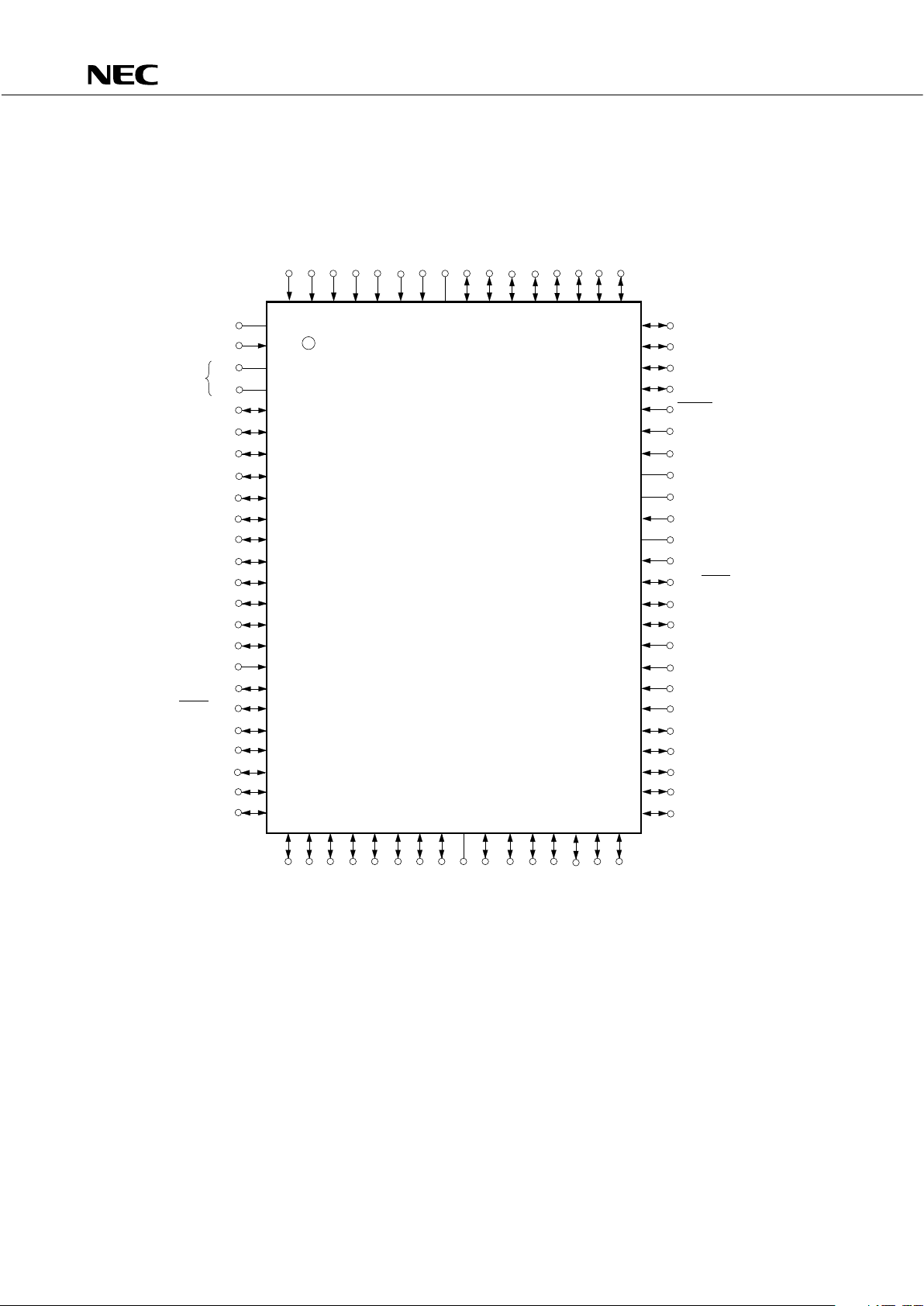
1. PIN CONFIGURATION
IC: Internally Connected (Connect directly to VSS)
*: Power must be supplied to both VDD pins.
AN0
PD75512GF(A)
– –3B9×××
µ
AN4/P150
P120
AV
SS
AN1
1
80
21
22
23
24
25 26
P93
2
3
4
5
6
7
8
9
10
11
12
13
14
15
16
17
18
19
20
64
27 28 29 30 31 32 33 34 35 36 37 38 39
40
AN2
AN3
AN5/P151
AN6/P152
AN7/P153
P121
P122
P123
P130
P131
P132
P133
AV
REF
V
DD
V
DD
*
P113
P112
P111
P110
P103
P102
P101
P100
P92
P91
P90
SI1/P83
SO1/P82
SCK1/P81
PPO/P80
KR7/P73
KR6/P72
KR5/P71
KR4/P70
KR3/P63
KR2/P62
KR1/P61
KR0/P60
P53
P52
P51
P50
V
SS
P43
P42
P41
P40
P33
P32
P31
63
62
61
60
59
58
57
56
55
54
53
52
51
50
49
48
47
46
45
44
43
42
41
P140
P141
P142
P143
RESET
X2
X1
IC
XT2
XT1
V
SS
P00/INT4
P01/SCK0
P02/SO0/SB0
P03/SI0/SB1
P10/INT0
P11/INT1
P12/INT2
P13/TI0
P20/PTO0
P21
P22/PCL
P23/BUZ
P30
79 78 77 76 75 74 73 72 71 70 69 68 67 66 65
µ
PD75512(A)
7
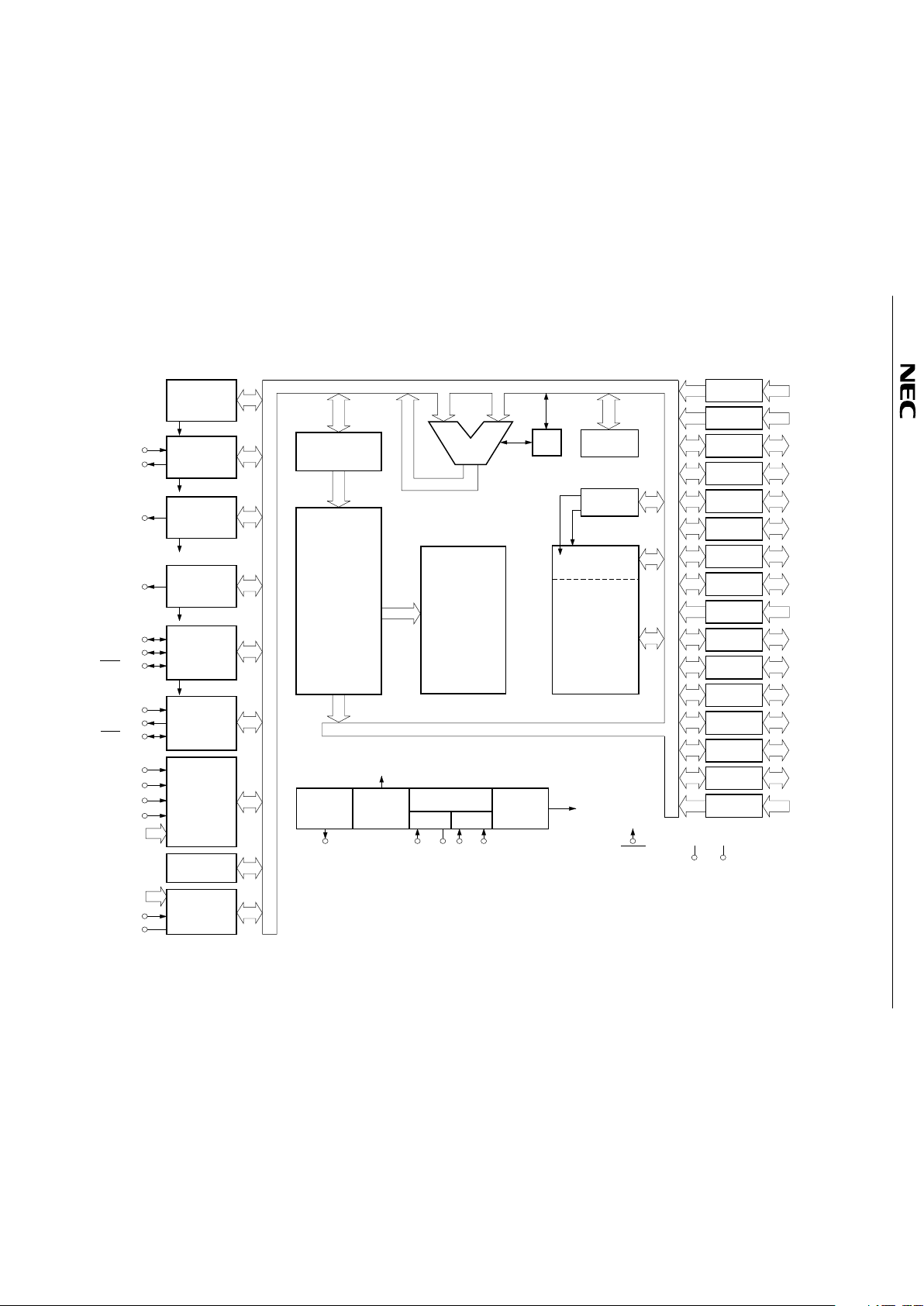
2. INTERNAL BLOCK DIAGRAM
PORT 0
PORT 1
PORT 2
PORT 3
PORT 4
PORT 5
PORT 6
PORT 7
PORT 8
PORT 9
PORT10
PORT11
PORT12
PORT13
PORT14
PORT15
44P10-P13
P00-P03
4 P20-P23
4
4 P30-P33
4 P40-P43*
4 P50-P53*
4 P60-P63
4 P70-P73
P80-P83
4 P90-P93
4 P100-P103
4 P110-P113
4 P120-P123*
4 P130-P133*
4 P140-P143*
P150-P153
4
SP (8)
BANK
GENERAL REG.
CY
ALU
PROGRAM
COUNTER (14)
ROM
PROGRAM
MEMORY
12160 × 8 BITS
DECODE
AND
CONTROL
RAM
DATA MEMORY
512 x 4 BITS
TI0/P13
TIMER/EVENT
COUNTER
#0
INTT0
PTO0/P20
BUZ/P23
WATCH
TIMER
INTW
INTCSI
SERIAL
INTERFACE0
SI0/SB1/P03
SO0/SB0/P02
SCK0/P01
INT0/P10
INT1/P11
INT2/P12
INT4/P00
KR0/P60
–KR7/P73
8
INTERRUPT
CONTROL
BIT SEQ.
BUFFER (16)
BASIC
INTERVAL
TIMER
INTBT
PPO/P80
TIMER/PULSE
GENERATOR
INTTPG
SERIAL
INTERFACE1
SI1/P83
SO1/P82
SCK1/P81
A/D
CONVERTER
AV
REF
AV
SS
AN0-AN3
AN4
/P150-AN7/P15
f /2
X
N
VDDV
SS
RESET
PCL/P22 XT1 XT2 X1 X2
SUB MAIN
CLOCK
OUTPUT
CONTROL
CLOCK
DIVIDER
CLOCK
GENERATOR
STAND BY
CONTROL
CPU CLOCK
4
Φ
*: PORTs 4, 5, and 12 to 14 are 10 V middle voltage, N-ch open-drain input/output ports.
µ
PD75512(A)
8
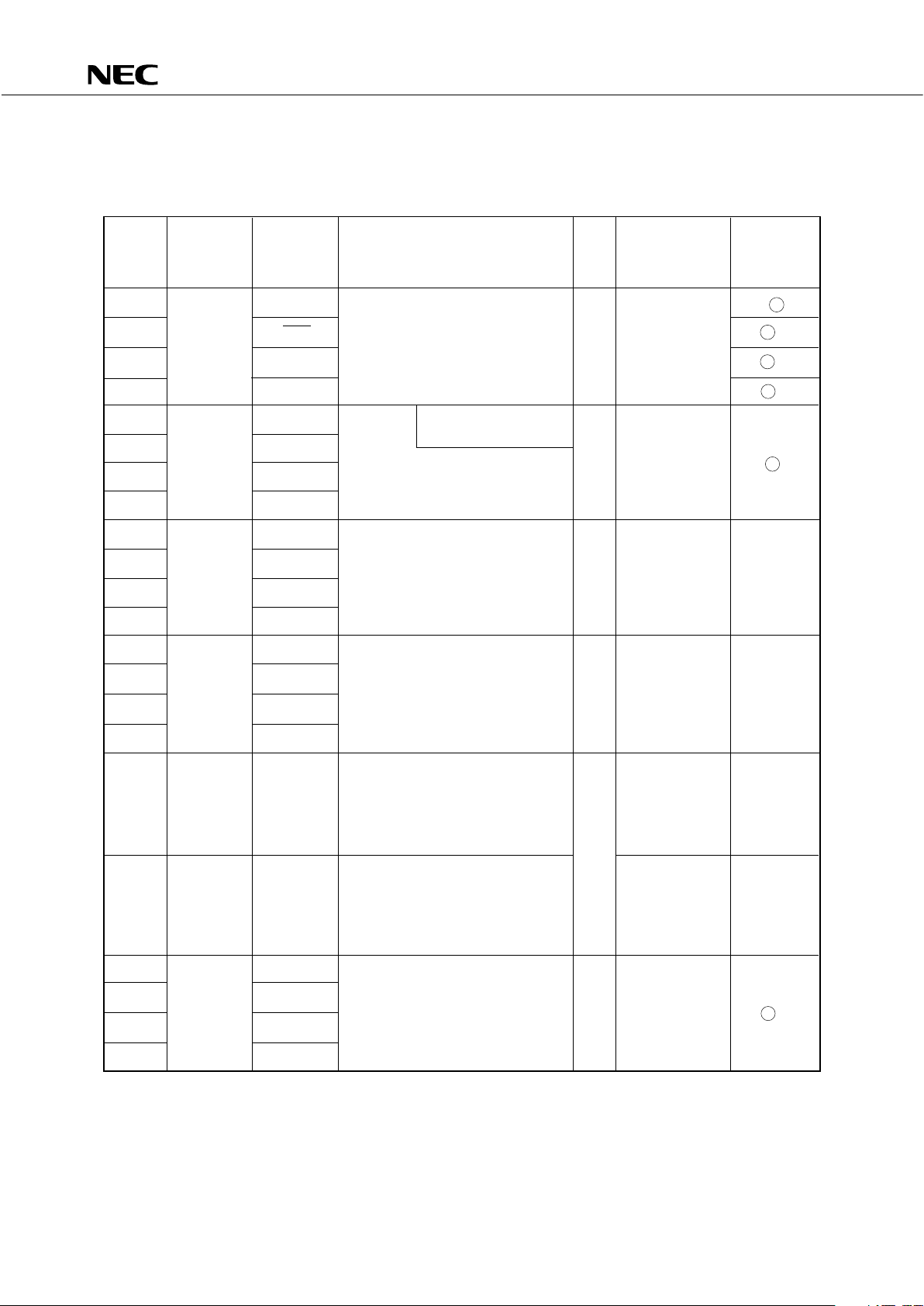
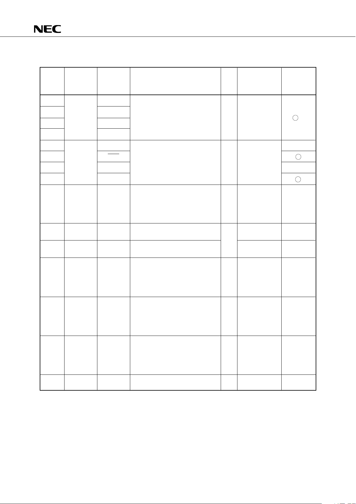
3. PIN FUNCTIONS
3.1 PORT PINS (1/2)
Input/
Pin Input/ Shared Function 8-bit When Reset Output
Name Output Pin I/O Circuit
Type*
P00 INT4 4-bit input port (PORT0). B
For P01 to P03, built-in pull-up
P01 SCK0 resistors can be specified in 3-bit F -A
Input units by software. x Input
P02 SO0/SB0 F -B
P03 SI0/SB1 M -C
P10 INT0 With noise
elimination function
P11 INT1
Input 4-bit input port (PORT1). x Input B -C
P12 INT2 Built-in pull-up resistors can be
specified by software in 4-bit units.
P13 TI0
P20 PTO0
4-bit input/output port (PORT2).
P21 Input/ — Built-in pull-up resistors can be
output specified by software in 4-bit units. x Input E-B
P22 PCL
P23 BUZ
P30 — Programmable 4-bit input/output
port (PORT3).
P31 Input/ — Input/output can be specified in
output bit units. x Input E-C
P32 — Built-in pull-up resistors can be
specified by software in 4-bit unit.
P33 —
N-ch open-drain 4-bit input/output High level
port (PORT4). (when pull-up
P40 to Input/ — A pull-up resistor can be provided resistor is M
P43 output in bit units (mask option). provided) or
10V withstanding voltage in the high impedance
open-drain mode.
O
N-ch open-drain 4-bit input/output High level
port (PORT5). (when pull-up
P50 to Input/ — A pull-up resistor can be provided resistor is M
P53 output in bit units (mask option). provided) or
10V withstanding voltage in the high impedance
open-drain mode.
P60 KR0 Programmable 4-bit input/ output
port (PORT6).
P61 Input/ KR1 Input/output can be specified in
output bit units. O Input F -C
P62 KR2 Built-in pull-up resistors can be
specified by software in 4-bit units.
P63 KR3
*: The number enclosed with a circle indicates Schmitt trigger input.
µ
PD75512(A)
9
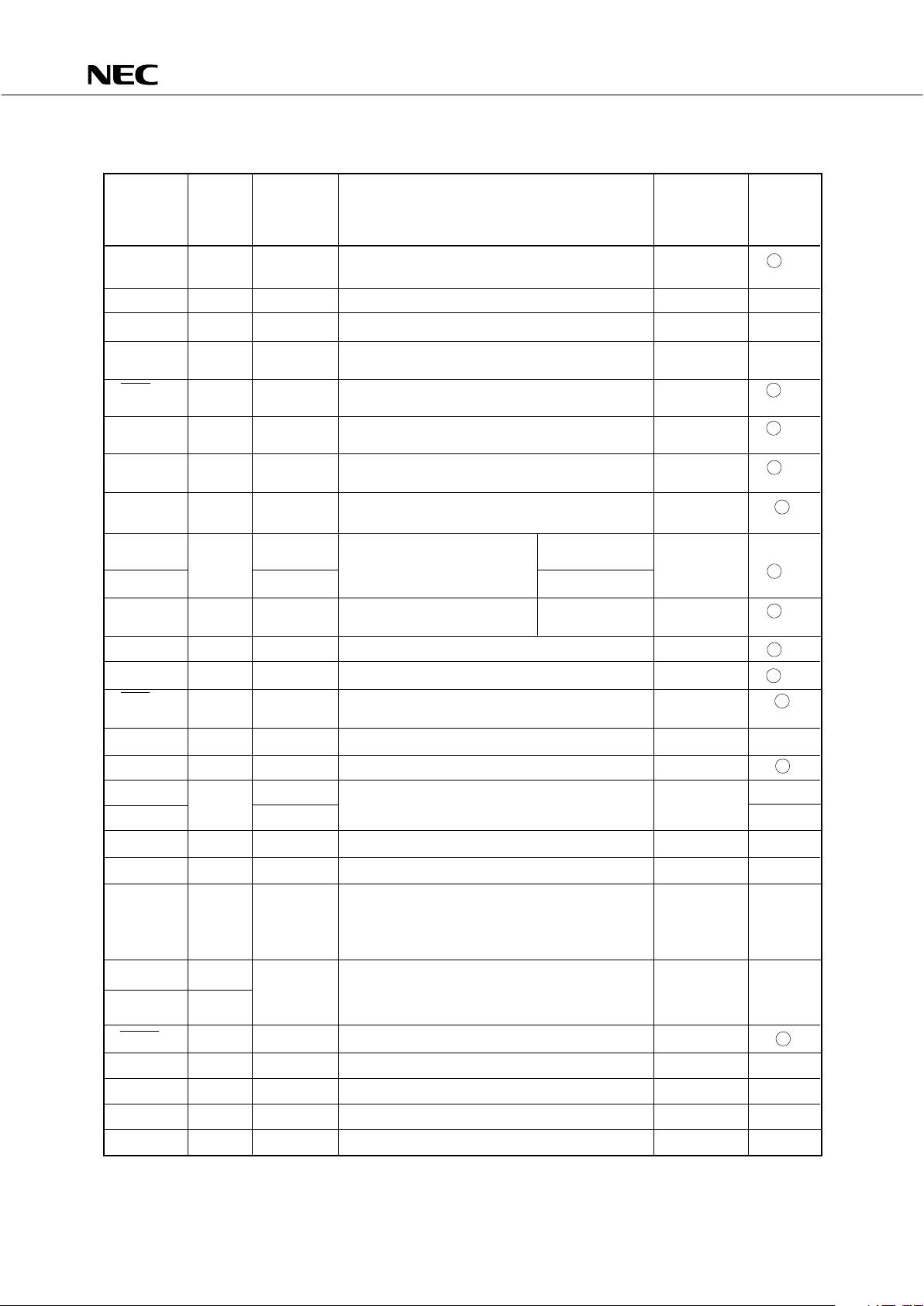
3.1 PORT PINS (2/2)
Input/
Pin Input/ Shared Function 8-bit When Reset Output
Name Output Pin I/O Circuit
Type*
P70 KR4
4-bit input/output port (PORT7).
P71 Input/ KR5 Built-in pull-up resistor can be
output specified in 4-bit units by software. O Input F -A
P72 KR6
P73 KR7
P80 PPO E
P81 SCK1 F
Input 4-bit input port (PORT8). x Input
P82 SO1 E
P83 SI1 B
Low level
4-bit input/output port (PORT9). (when pullP90 to Input/ — Built-in pull-up resistors can be x down resistor V
P93 output specified in bit units by mask is provided)
option. or high
impedance
P100 to Input/ — 4-bit input/output port (PORT10). Input E
P103 output
x
P110 to Input/ — 4-bit input/output port (PORT11). Input E
P113 output
N-ch open-drain 4-bit input/output High level
port (PORT12). (when pull-up
P120 to Input/ — A pull-up resistor can be provided resistor is M
P123 output in bit units (mask option). x provided) or
10V withstanding voltage in the high impedance
open-drain mode.
N-ch open-drain 4-bit input/output High level
port (PORT13). (when pull-up
P130 to Input/ — A pull-up resistor can be provided x resistor is M
P133 output in bit units (mask option). provided) or
10V withstanding voltage in the high impedance
open-drain mode.
N-ch open-drain 4-bit input/output High level
port (PORT14). (when pull-up
P140 to Input/ — A pull-up resistor can be provided x resistor is M
P143 output in bit units (mask option). provided) or
10V withstanding voltage in the high impedance
open-drain mode.
P150 to Input AN4 to AN7 4-bit input port (PORT15). x Input Y-A
P153
*: The number enclosed with a circle indicates Schmitt trigger input.
µ
PD75512(A)
10
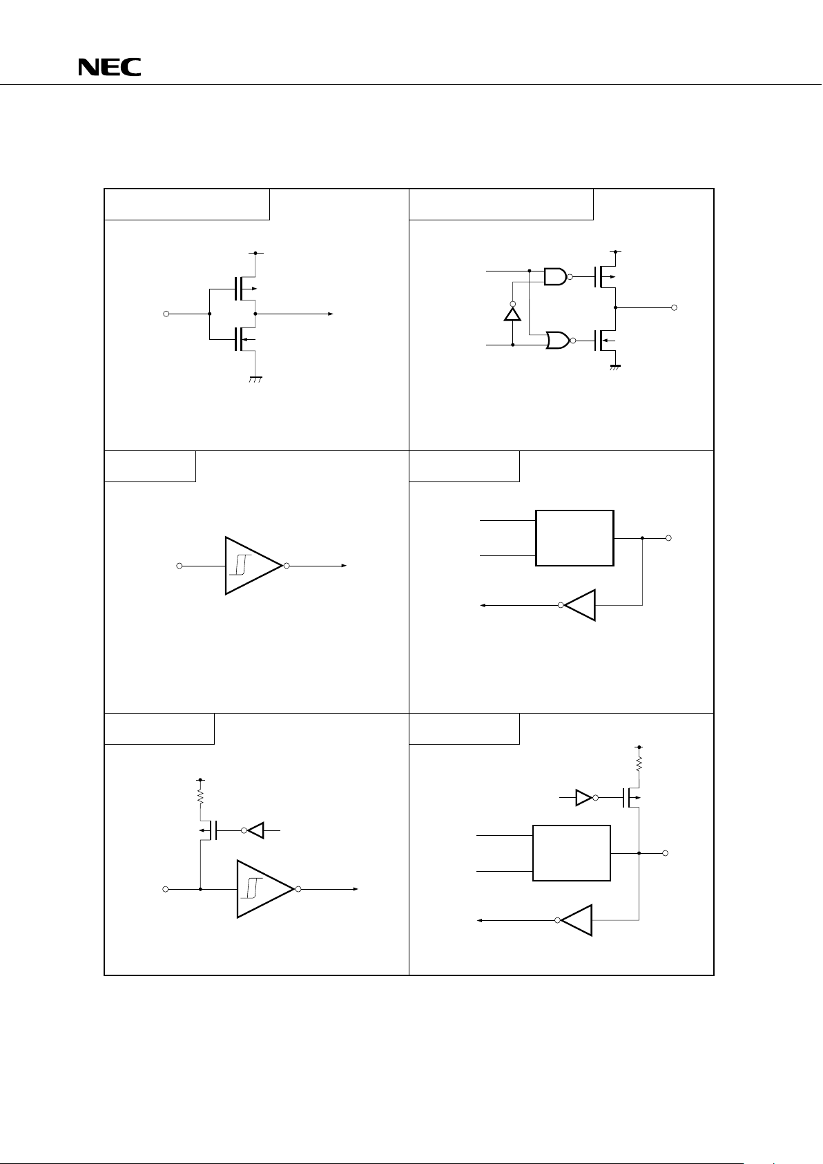
3.2 NON-PORT PINS
Input/
Pin Input/ Shared Function When Reset Output
Name Output Pin Circuit
Type*
TI0 Input P13 The external event pulse input for the timer/event — B -C
counter.
PTO0 Output P20 Timer/event counter output Input E-B
PCL Output P22 Clock output Input E-B
BUZ Output P23 Fixed frequency output (for buzzer output or Input E-B
system clock trimming)
SCK0 Input/ P01 Serial clock input/output Input F -A
output
SO0/SB0 Input/ P02 Serial data output Input F -B
output Serial bus input/output
SI0/SB1 Input/ P03 Serial data input Input M -C
output Serial bus input/output
INT4 Input P00 Edge detection vector interrupt input (both rising — B
edge and falling edge detection)
INT0 P10 Edge detection vector Synchronized
interrupt input with clock
Input (detection edge selectable) — B -C
INT1 P11 Asynchronous
INT2 Input P12 Edge detection testable input Asynchronous — B -C
(rising edge detection)
KR0-KR3 Input P60-P63 Parallel falling edge detection testable input Input F -C
KR4-KR7 Input P70-P73 Parallel falling edge detection testable input Input F -A
SCK1 Input/ P81 Serial clock input/output Input F
output
SO1 Output P82 Serial data output Input E
SI1 Input P83 Serial data input Input B
AN0-AN3 — Y
Input A/D converter analog input —
AN4-AN7 P150-P153 Y-A
AVREF Input — A/C converter reference voltage input — Z
AVSS — — A/D converter reference ground — —
Pins for connecting the crystal ceramic oscillator
to the main system clock generator. When
X1, X2 Input — inputting the external clock, input the external — —
clock to pin X1, and the reverse phase of the
external clock to pin X2.
XT1 Input Pins for connecting the crystal oscillator to the
— subsystem clock generator. When the external — —
clock is used, inputs the external clock to pin
XT1. In this case, pin XT2 must be left open.
RESET Input — System reset input — B
PPO Output P80 Timer/pulse generator pulse output Input E
IC — — Internally Connected. Connect directly to VSS.——
VDD — — Positive power supply — —
VSS — — GND — —
*: The number enclosed with a circle indicates Schmidt trigger input.
XT2 —
µ
PD75512(A)
11
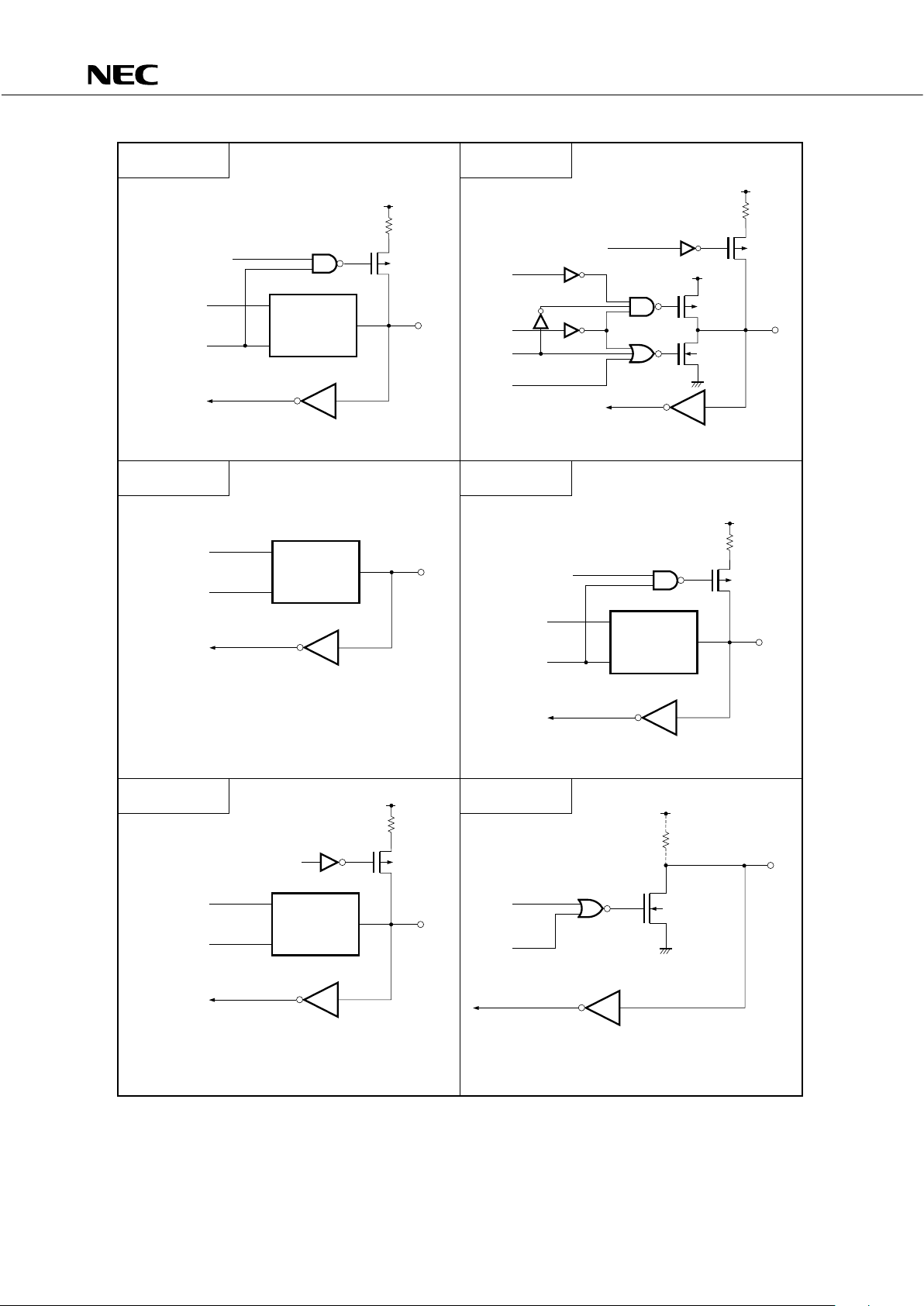
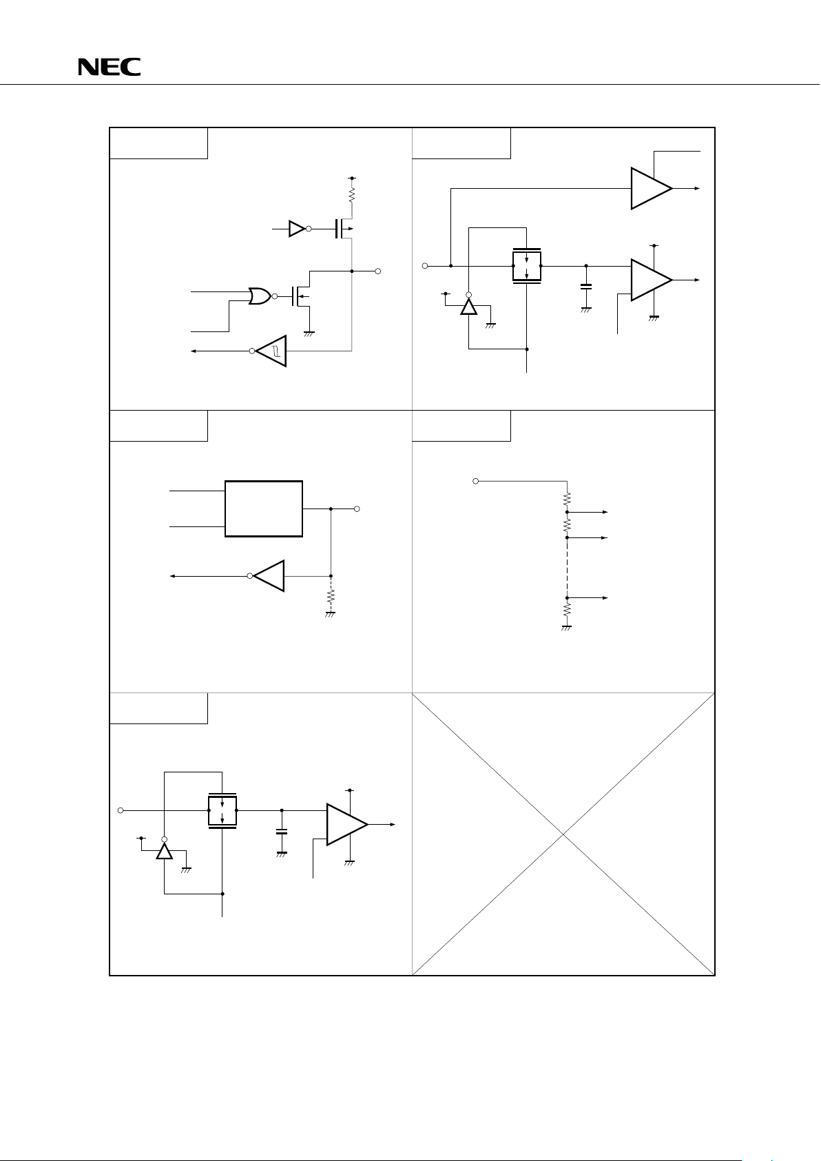
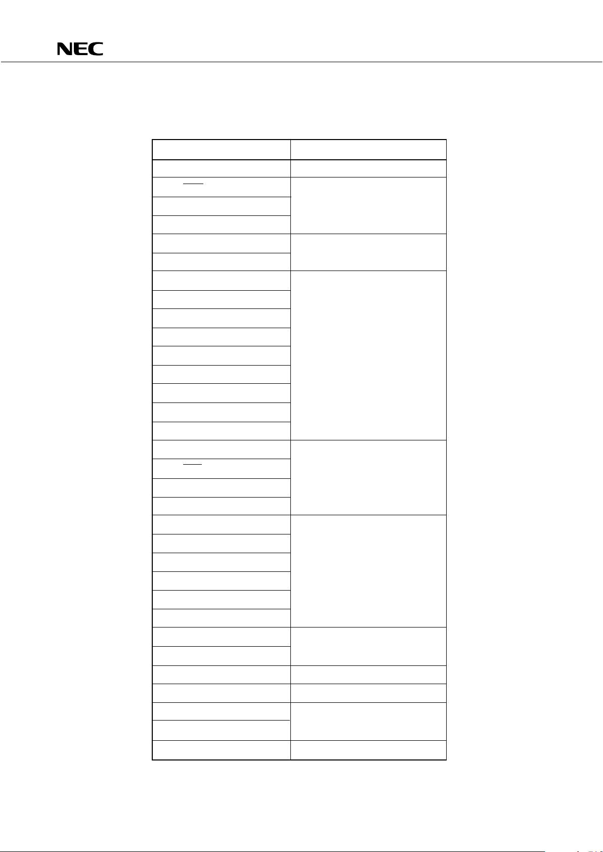
3.3 PIN INPUT/OUTPUT CIRCUITS
The following shows a simplified input/output circuit diagram for each pin of the
µ
PD75512(A).
TYPE A
TYPE D
TYPE B
TYPE E
IN
V
DD
Input buffer of CMOS standard
data
output
disable
OUT
P–ch
N–ch
Push-pull output that can be set in a output
high-impedance state (both P-ch and N-ch are off)
IN
Schmitt trigger input with hysteresis characteristics
data
output
disable
Type D
Type A
IN/OUT
This input/output circuit consists of D-type push-pull
outputs and Type A input buffers.
P.U.R.
enable
V
DD
P.U.R.
P–ch
TYPE B–C
TYPE E
–
B
IN
data
output
disable
Type D
Type A
P.U.R.
enable
V
DD
P.U.R.
P–ch
IN/OUT
Schmitt trigger input with hysteresis characteristics
VDD
P.U.R. : Pull-Up Resistor
P.U.R. : Pull-Up Resistor
P–ch
N–ch
Fig. 3-1 Pin Input/Output Circuits (1/3)
µ
PD75512(A)
12
Type E-C
data
output
disable
Type D
Type A
P.U.R.
enable
V
DD
P.U.R.
P–ch
IN/OUT
Type F-B
data
output
disable
P.U.R.
enable
V
DD
P.U.R.
P–ch
N-ch
P-ch
output
disable
(P-ch)
output
disable
(N-ch)
V
DD
IN/OUT
Type B
Type F Type F-C
data
output
disable
Type D
Type B
P.U.R.
enable
V
DD
P.U.R.
P–ch
IN/OUT
data
output
disable
Type D
Type B
IN/OUT
This input/output circuit consists of D-type push-pull
outputs and Type B Schmitt trigger inputs.
Type F-A Type M
data
output
disable
V
DD
P.U.R.
IN/OUT
N-ch
Middle-voltage input buffer
(can withstand up to +10 V)
data
output
disable
Type D
Type B
P.U.R.
enable
V
DD
P.U.R.
P–ch
IN/OUT
(can withstand
up to +10 V)
P.U.R. : Pull-Up Resistor P.U.R. : Pull-Up Resistor
P.U.R. : Pull-Up Resistor
P.U.R. : Pull-Up Resistor
P.U.R. : Pull-Up Resistor
(Mask Option)
Fig. 3-1 Pin Input/Output Circuits (2/3)
µ
PD75512(A)
13
Type M-C
Type Y-A
Type V
Type Z
data
output
disable
P.U.R.
enable
V
DD
P.U.R.
IN/OUT
P–ch
N-ch
N–ch
IN
P–ch
AV
SS
V
DD
V
DD
AV
SS
Sampling
C
+
–
input
enable
Reference voltage
(from a voltage tap of series
resistor string)
IN instruction
data
output
disable
Type D
Type A
IN/OUT
AV
AV
SS
Reference voltage
REF
P.D.R
(Mask Option)
N–ch
IN
P–ch
AV
SS
V
DD
V
DD
AV
SS
Sampling
C
+
–
Input
enable
Reference voltage
(from a voltage tap of series
resistor string)
P.U.R. : Pull-Up Resistor
P.D.R. : Pull-Down Resistor
Type Y
Fig. 3-1 Pin Input/Output Circuits (3/3)
µ
PD75512(A)
14
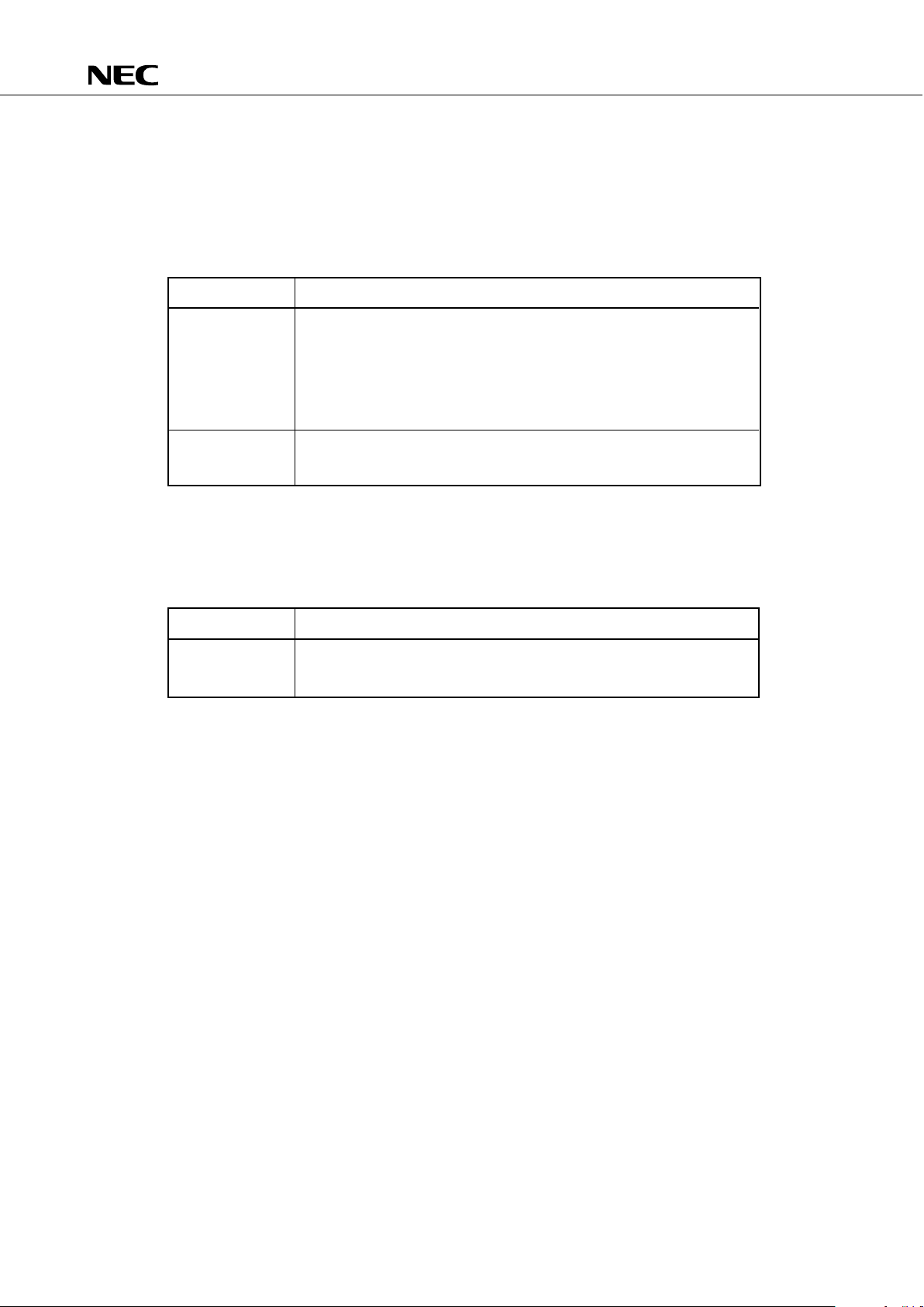
3.4 RECOMMENDED CONDITIONS FOR UNUSED PINS
Table 3-1 Recommended Conditions for Unused Pins
Pin Recommended Conditions
P00/INT4 Connect to VSS
P01/
SCK0
P02/SO0/SB0 Connect to VSS or VDD
P03/SI1/SB1
P10/INT0-P12/INT2
Connect to VSS
P13/TI0
P20/PTO0
P21
P22/PCL
P23/BUZ
Input state: Connect to VSS or VDD
P30-P33
Output state: Open
P40-P43
P50-P53
P60/KR0-P63/KR3
P70/KR4-P73/KR7
P80/PPO
P81/
SCK1
Connect to VSS or VDD
P82/SO1
P83/SI1
P90-P93
P100-P103
P110-P113 Input state: Connect to VSS or VDD
P120-P123 Output state: Open
P130-P133
P140-P143
P150/AN4-P153/AN7
Connect to VSS
AN0-AN3
XT1 Connect to VSS or VDD
XT2 Open
AVREF
Connect to VSS
AVSS
IC Connect directly to VSS
★
µ
PD75512(A)
15
3.5 MASK OPTION SELECTION
The following mask options are provided with the pins.
(1) Pull-up/pull-down resistor selection
Table 3-2 Pull-up/Pull-down Resistor Selection
Pins Mask Option
P40-P43 (1) With pull-up resistor (2) Without pull-up resistor
P50-P53 (Can be specified in bit units) (Can be specified in bit units)
P120-P123
P130-P133
P140-P143
P90-P93 (1) With pull-down resistor (2) Without pull-down resistor
(Can be specified in bit units) (Can be specified in bit units)
(2) Feedback resistor selection for the subsystem clock oscillation
Table 3-3 Feedback Resistor Selection
Pins Mask Option
XT1, XT2 (1) With feedback resistor (2) Without feedback resistor
(When the subsystem clock (When the subsystem clock
is used) is not used)
Note: The operation is not affected if the feedback resistor is selected when the subsystem
clock is not used. However, the supply current I
DD is increased.
★

µ
PD75512(A)
16
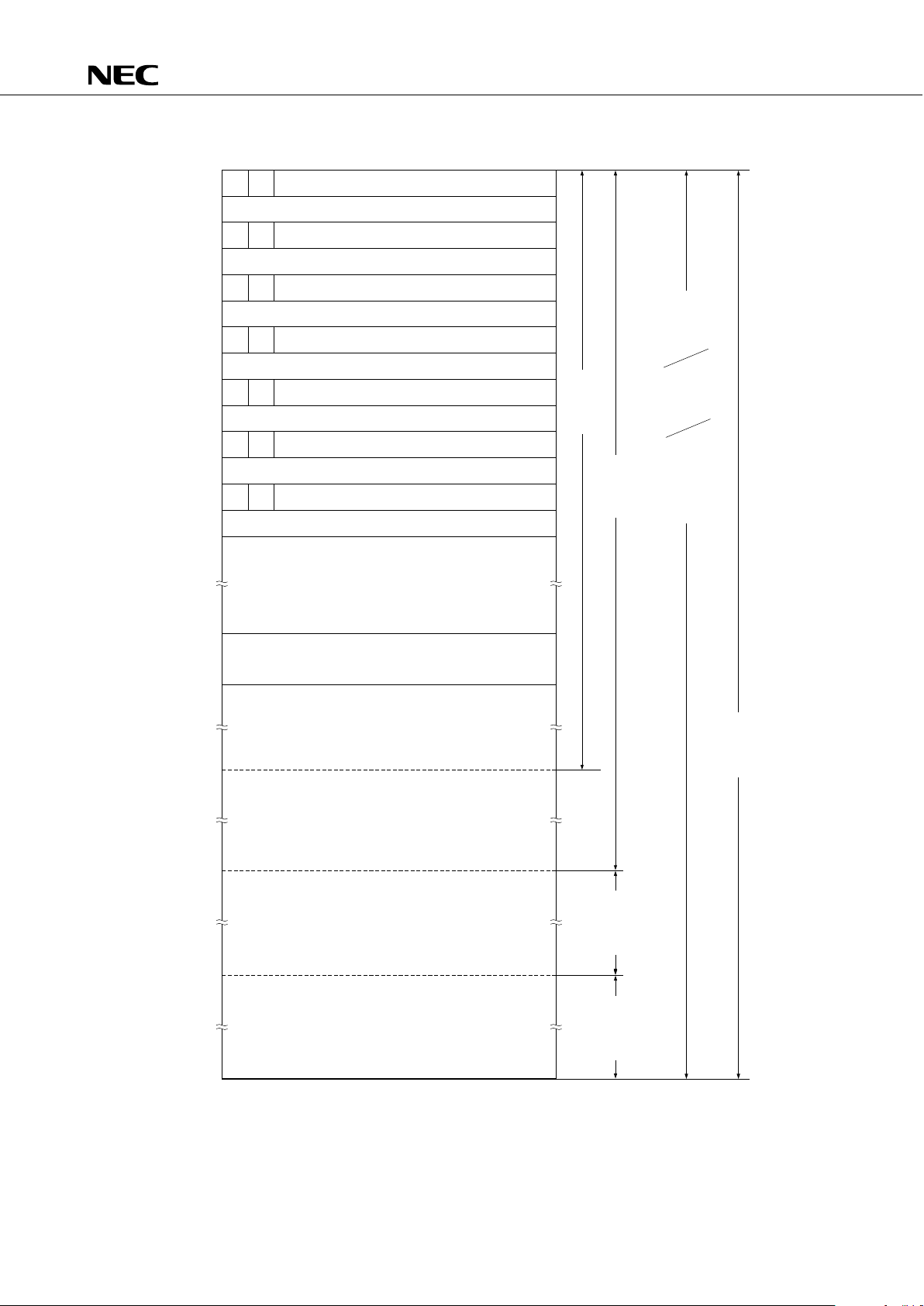
4. MEMORY CONFIGURATION
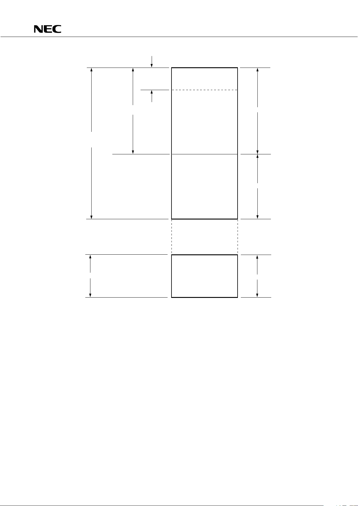
• Program memory (ROM) ... 12160 × 8 bits (0000H-2F7FH)
• 0000H, 0001H : Vector table to which address from which program is started is written after reset
• 0002H-000DH : Vector table to which address from which program is started is written after
interrupt
• 0020H-007FH: Table area referenced by GETI instruction
• Data memory
• Data area .... 512 × 4 bits (000H–1FFH)
• Peripheral hardware area .... 128 × 4 bits (F80H–FFFH)
★
µ
PD75512(A)
17
76
MBE
MBE
MBE
MBE
MBE
MBE
Internal reset start address (upper 6 bits)
Internal reset start address (lower 8 bits)
INTBT/INT4 start address (upper 6 bits)
INTBT/INT4 start address (lower 8 bits)
INT0 start address (upper 6 bits)
INT0 start address (lower 8 bits)
INT1 start address (upper 6 bits)
INT1 start address (lower 8 bits)
INTCSIO0 start address (upper 6 bits)
INTCSIO0 start address (lower 8 bits)
INTT0 start address (upper 6 bits)
INTT0 start address (lower 8 bits)
0000H
0002H
0004H
0006H
0008H
000AH
0020H
007FH
0080H
007FH
0800H
0FFFH
1000H
1FFFH
GETI instruction reference table
0
CALLF
!faddr
instruction
entry
address
Address
2000H
2F7FH
BRCB
!caddr
instruction
branch
address
BRCB
!caddr
instruction
branch
address
RBE
RBE
RBE
RBE
RBE
RBE
MBE
INTTPG start address (upper 6 bits)000CH
RBE
INTTPG start address (lower 8 bits)
BR !addr
instruction
branch address
CALL !addr
instruction
subroutine
entry address
BR $addr
instruction
relational
branch address
(–15 to –1,
+2 to +16)
Branch destination
address and
subroutine entry
address for
GETI instruction
BRCB
!caddr
instruction
branch
address
Remarks: In addition to the above, branching to an address, for which only the lower 8 bits of the PC are
modified, is possible by the BR PCDE and BR PCXA instructions.
Fig. 4-1 Program Memory Map
µ
PD75512(A)
18
Data memory
Memory bank
General
purpose
register
area
000H
01FH
008H
(32 × 4)
256× 4
Stack
area
100H
0FFH
Data area
Static RAM
(512× 4)
1FFH
256× 4
Unmapped
F80H
128× 4
FFFH
Peripheral hardware area
15
1
0
Fig. 4-2 Data Memory Map

µ
PD75512(A)
19
5. PERIPHERAL HARDWARE FUNCTIONS
5.1 PORT
I/O ports are classified into following kinds:
• CMOS input (PORTS 0, 1, 8, 15) : 16
• CMOS input/output (PORTS 2, 3, 6, 7, 9, 10, 11) : 28
• N-ch open-drain input/output (PORTS 4, 5, 12, 13, 14) : 20
Total : 64
Table 5-1 Port Functions
Port
Function Operation/Feature Remarks
(Pin Name)
Also serves as the INT4,
SCK0
,
Can be read or tested regardless of the operation SO0/SB0, and SI0/SB1 pins
4-bit input mode of the shared pin.
Also serves as INT0 to 2, and
TIO pins
Can be specified for I/O in 4-bit units Also serves as PTO0, PCL and
4-bit I/O BUZ pins.
Can be specified for I/O in 1/4-bit units. —
4-bit I/O Whether or not the internal
(N-ch Can be specifiedfor pull-up resistor is provided
open-drain, I/O in 4-bit units can be specified for each bit
can sustain by mask option
with 10V)
Can be specified
for I/O in 1/4-bit units Ports 6 and 7 can Also serves as KR0-3.
4-bit I/O be paired to I/O
Can be specified data in 8-bit units
I/O in 4-bit Also serves as KR4-7.
units
4-bit Can be read or tested regardless of the operation Also serves as PPO,
SCK1
,
input mode of the shared pin. SO1, and SI1 pins.
Whether or not the internal
pull-up resistor is provided
can be specified for each bit
by mask option.
PORT10
4-bit I/O Can be specified for I/O in 4-bit units. —
PORT11
PORT12 4-bit I/O Whether or not the internal
(N-ch pull-up resistor is provided
PORT13 open-drain, Can be specified for I/O in 4-bit units. can be specified for each
can sustain bit by mask option.
PORT14 with 10V)
PORT15 4-bit Can be read or tested regardless of the operation Also serves as AN4-7 pins.
Input mode of the shared pins
PORT9 4-bit I/O Can be specified for I/O in 4-bit units.
PORT8
PORT0
PORT1
PORT2
PORT4
PORT3
PORT5
PORT7
PORT6
Ports 4 and 5 can
be paired to I/O
data in 8-bit units
★
µ
PD75512(A)
20
6.2 CLOCK GENERATOR CIRCUIT
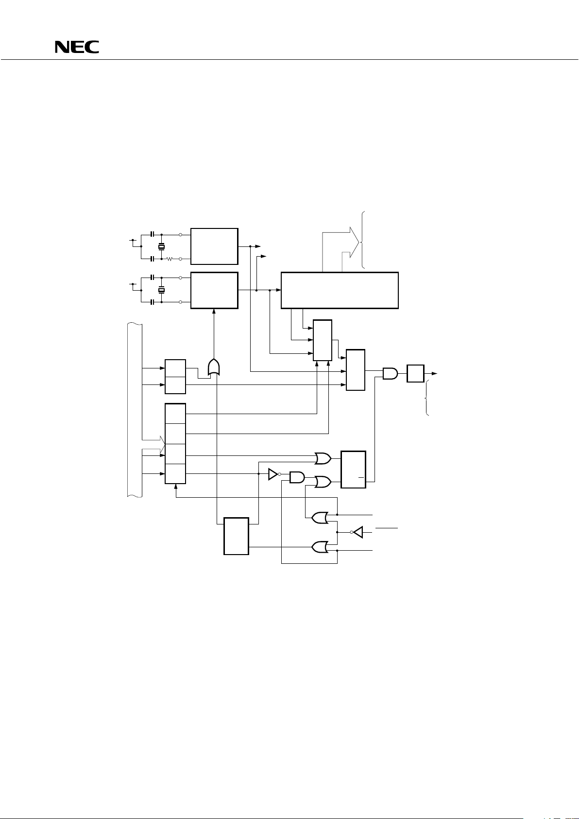
The operation of the clock generator circuit is determined by the processor clock control regiser (PPC) and
system clock control register (SCC).
This circuit can generate two types of clocks: main system clock and subsystem clock.
In addition, it can also change the instruction execution time.
• 0.95
µ
s, 1.91 µs, 15.3 µs (main system clock: 4.19 MHz)
• 122
µ
s (subsystem clock: 32.768 kHz)
*: instruction execution.
Remarks 1: f
X = Main system clock frequency
2: f
XT = Subsystem clock frequency
3: Φ= CPU clock
4: PCC: Processor clock control register
5: SCC: System clock control register
6: One clock cycle (tCY) of Φ is one machine cycle of an instruction. For tCY, refer to AC
characteristics in 10. ELECTRICAL SPECIFICATIONS.
Fig. 5-1 Clock Generator Block Diagram
V
DD
V
DD
XT1
XT2
X1
X2
f
XT
f
X
Watch timer
Subsystem
clock
oscillator
Main system
clock
oscillator
1/2 1/16
1/8 to 1/4096
Frequency divider
· Basic interval timer (BT)
· Timer/event counter
· Serial interface
· Watch timer
· Clock output circuit
· A/D converter
· INT0 noise rejecter circuit
Internal bus
WM.3
SCC
SCC3
SCC0
PCC
PCC0
PCC1
PCC2
PCC3
HALT*
STOP*
4
PCC2, PCC3
clear signal
STOP F/F
QS
R
Q
S
R
HALT F/F
Oscillator
disable
signal
Frequency
divider
1/4
Selector
Φ
· CPU
· Clock output
circuit
· INT0 noise
rejecter circuit
Wait release
signal from BT
RESET signal
Standby release
signal from interrupt
control circuit
Timer/pulse
generator
Selector
 Loading...