NEC UPD72107GC-3B9, UPD72107L, UPD72107CW Datasheet

DATA SHEET
MOS INTEGRATED CIRCUIT
µ
PD72107
LAP-B CONTROLLER
Link Access Procedure Balanced mode
The µPD72107 is an LSI that supports LAP-B protocol specified by the ITU-T recommended X.25 on a single
chip.
FEATURES
• Complied with ITU-T recommended X.25 (LAP-B84
edition)
HDLC frame control
Sequence control
Flow control
• ITU-T recommended X.75 supported
• TTC standard JT-T90 supported
• Optional functions
Option frame
Global address frame
Error check deletion frame
• Powerful test functions
Data loopback function
Loopback test link function
Frame trace function
• Abundant statistical information
• Detailed mode setting function
• Modem control function
• On-chip DMAC (Direct Memory Access Controller)
24-bit address
Byte/word transfer enabled (switch with external pin)
• Memory-based interface
Memory-based command
Memory-based status
Memory-based transmit/receive data
• MAX.4 Mbps serial transfer rate
• NRZ, NRZI coding
ORDERING INFORMATION
Part Number Package
µ
PD72107CW 64-pin plastic shrink DIP (750 mils)
µ
PD72107GC-3B9 80-pin plastic QFP (14 x 14 mm)
µ
PD72107L 68-pin plastic QFJ (950 x 950 mils)
The information in this document is subject to change without notice.
Document No. S12962EJ5V0DS00 (5th edition)
Date Published October 1998 N CP(K)
Printed in Japan
©
1998

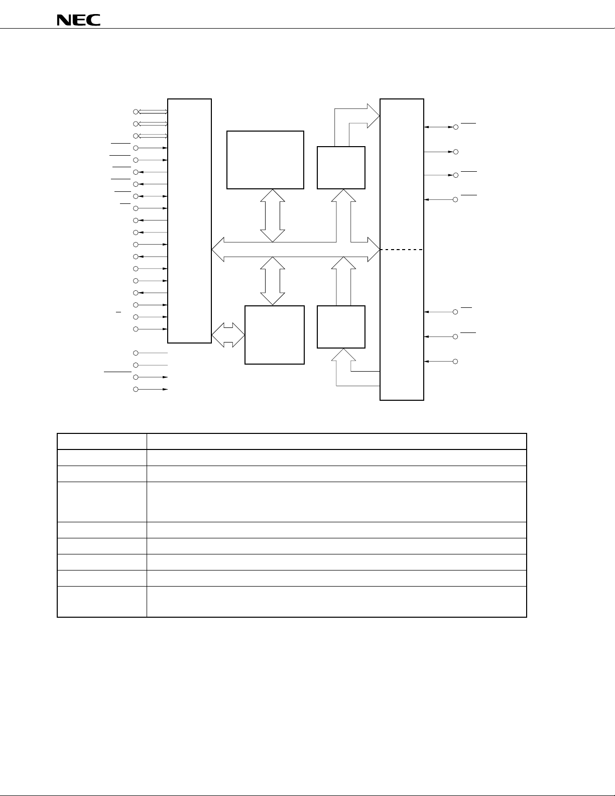
BLOCK DIAGRAM
D0-D7
A16D8
-A23D15
A0-A15
IORD
IOWR
MRD
MWR
UBE
CS
ASTB
AEN
READY
HLDRQ
HLDAK
CRQ
INT
CLRINT
B/W
PU
VCC
GND
RESET
CLK
Bus
interface
Internal controller
Internal bus
DMAC
TxFIFO
RxFIFO
Transmitter
Receiver
µ
TxC
TxD
RTS
CTS
CD
RxC
RxD
PD72107
Name Function
Bus interface An interface between the µPD72107 and external memory or external host processor
Internal controller Manages LAP-B protocol including control of the DMAC block, transmitter block, and receiver block
DMAC Controls the transfer of data on the external memory to the internal controller or transmitter block,
(Direct Memory and controls the writing of data in the internal controller or receiver block to the external memory
Access Controller)
TxFIFO A 16-byte buffer for when transmit data is sent from the DMAC to the transmitter block
RxFIFO A 32-byte buffer for when receive data is sent from the receiver block to the DMAC
Transmitter Converts the contents of TxFIFO into an HDLC frame and transmits it as serial data
Receiver Receives HDLC frame and writes internal data to RxFIFO
Internal bus An 8-bit address bus and 8-bit data bus that connect the internal controller, DMAC, FIFO, serial block,
and bus interface block
2

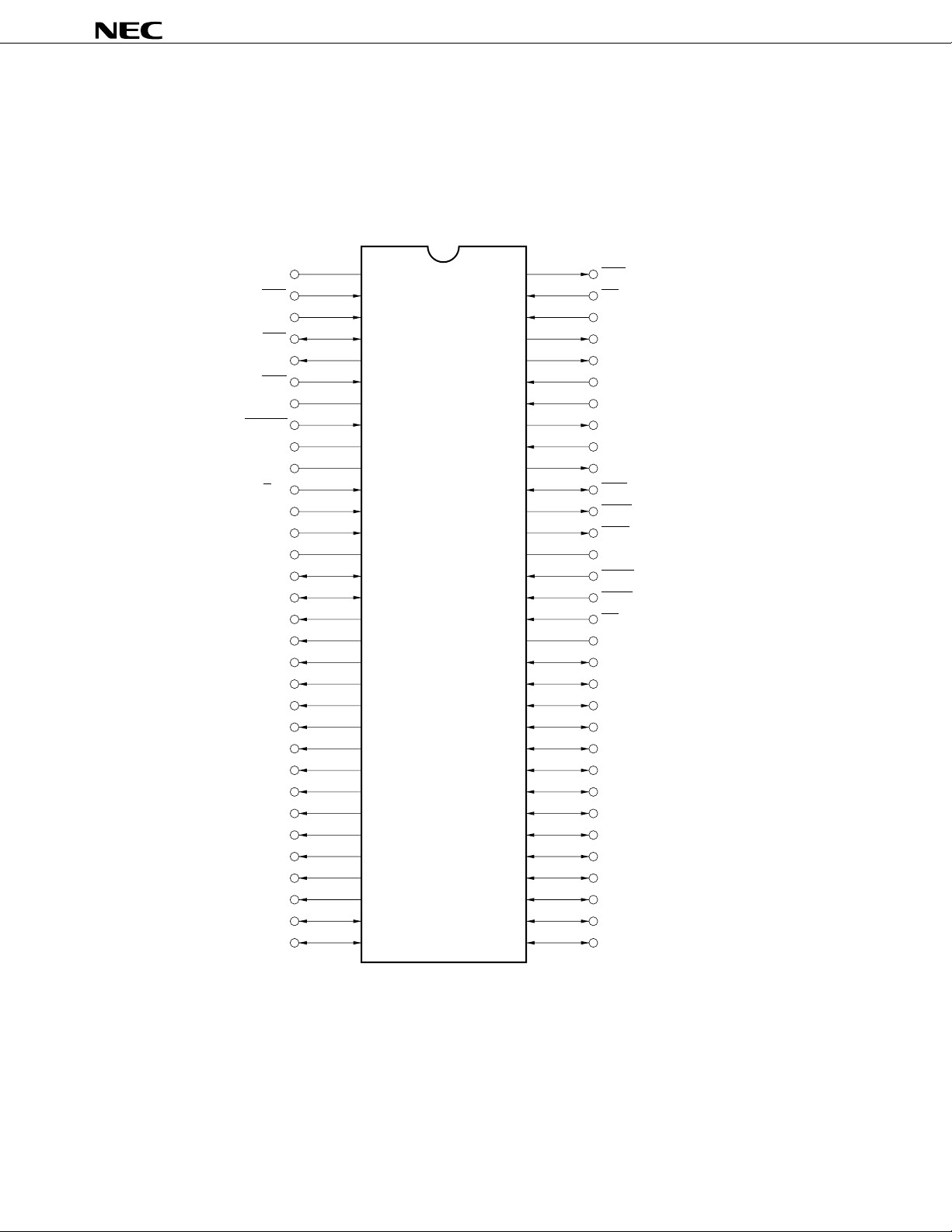
PIN CONFIGURATION (Top View)
64-pin plastic shrink DIP (750 mils)
µ
PD72107CW
µ
PD72107
RxC
RxD
TxC
TxD
CTS
RESET
NC
B/W
PU
CLK
GND
A0
A1
A2
A3
A4
A5
A6
A7
A8
A9
A10
A11
A12
A13
A14
A15
A16D8
A17D9
IC
IC
IC
1
2
3
4
5
6
7
8
9
10
11
12
13
14
15
16
17
18
19
20
21
22
23
24
25
26
27
28
29
30
31
32
64
63
62
61
60
59
58
57
56
55
54
53
52
51
50
49
48
47
46
45
44
43
42
41
40
39
38
37
36
35
34
33
RTS
CD
CRQ
AEN
ASTB
READY
HLDAK
HLDRQ
CLRINT
INT
UBE
MWR
MRD
GND
IOWR
IORD
CS
CC
V
D7
D6
D5
D4
D3
D2
D1
D0
A23D15
A22D14
A21D13
A20D12
A19D11
A18D10
3

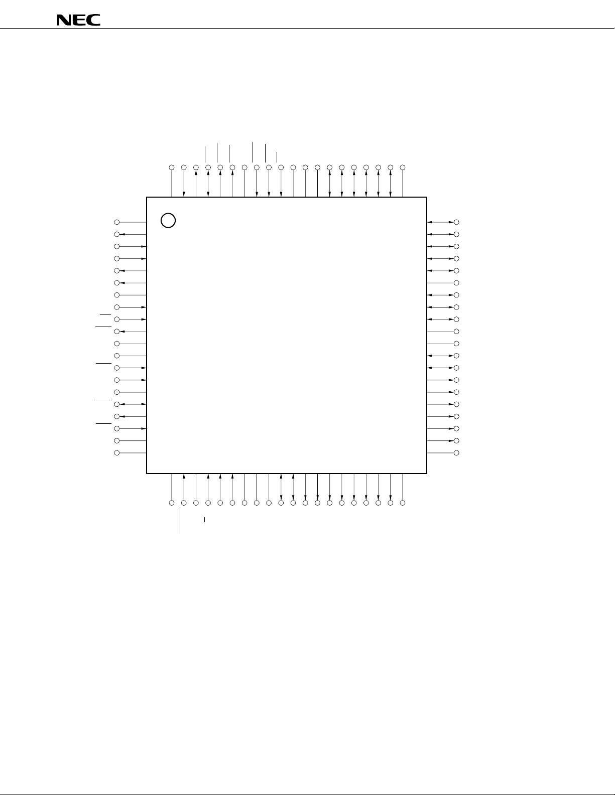
80-pin plastic QFP (14 × 14 mm)
µ
PD72107GC-3B9
NC
CLRINT
INT
80 79 78 77 76 75 74 73 72 71 70 69 68 67 66 65 64 63 62 61
UBE
MWR
MRD
GND
IOWR
IORDCSVCCNCVCCD7D6D5D4D3D2
NC
µ
PD72107
NC
HLDRQ
HLDAK
READY
ASTB
AEN
NC
CRQ
CD
RTS
NC
IC
RxC
RxD
NC
TxC
TxD
CTS
IC
NC
1
2
3
4
5
6
7
8
9
10
11
12
13
14
15
16
17
18
19
20
21 22 23 24 25 26 27 28 29 30 31 32 33 34 35 36 37 38 39 40
NC
IC
RESET
B/W
PU
CLK
GND
A0A1A2A3A4A5A6A7A8
NC
GND
A9
NC
60
59
58
57
56
55
54
53
52
51
50
49
48
47
46
45
44
43
42
41
D1
D0
A23D15
A22D14
A21D13
NC
A20D12
A19D11
A18D10
NC
NC
A17D9
A16D8
A15
A14
A13
A12
A11
A10
NC
4

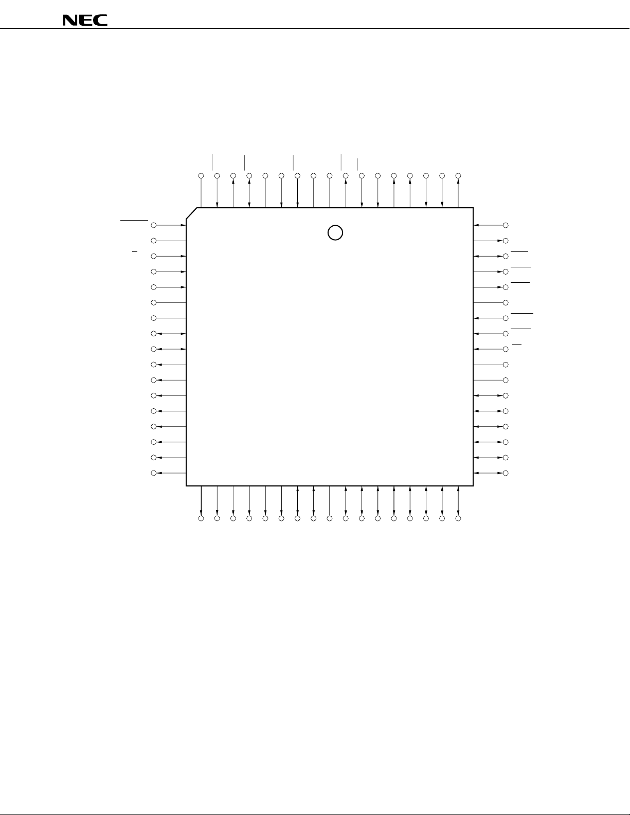
68-pin plastic QFJ (950 × 950 mils)
Q
µ
PD72107L
IC
CTS
TxD
9876543216867666564636261
RESET
IC
B/W
PU
CLK
GND
GND
A0
A1
A2
A3
A4
A5
A6
A7
A8
A9
10
11
12
13
14
15
16
17
18
19
20
21
22
23
24
25
26
27 28 29 30 31 32 33 34 35 36 37 38 39 40 41 42 43
TxCNCRxD
RxCICNC
RTSCDCRQ
AEN
ASTB
READY
HLDAK
HLDR
60
59
58
57
56
55
54
53
52
51
50
49
48
47
46
45
44
µ
PD72107
CLRINT
INT
UBE
MWR
MRD
GND
IOWR
IORD
CS
V
CC
VCC
D7
D6
D5
D4
D3
D2
A10
A11
A12
A13
A14
A15
A16D8
A17D9
NC
A18D10
A19D11
A20D12
A21D13
A22D14
A23D15
D0
D1
5

1. PINS
1.1 Pin Functions
µ
PD72107
SDIP QFP QFJ Active
Pin No. Pin No. Pin No. Level
V
CC 47 68 50 – – +5 V power supply
70 51
GND 14 27 15 – – Ground (0 V)
51 28 16 Note that there is more than one ground pin.
74 55
CLK 13 26 14 I – System clock input
(Clock) Input clock of 1 MHz to 8.2 MHz.
RESET 8 22 10 I L Initializes the internal
(Reset) more than 7 CLK clock cycles is required (clock
PU 12 25 13 I – Pull up to high level when using in normal operation.
(Pull Up)
CS 48 71 52 I L When bus master
(Chip Select) Set to disable.
MRD 52 75 56 O L When bus master
(Memory Read) 3-state Reads the data of the external memory at low level.
MWR 53 76 57 O L When bus master
(Memory Write) 3-state Writes the data to the external memory at low level.
IORD 49 72 53 I L This pin is used when the external host processor
(I/O Read) reads the contents of the internal registers of the
IOWR 50 73 54 I L This pin is used when the external host processor
(I/O Write) writes the data to the internal registers of the
ASTB 60 5 64 O H This pin is used to latch the address output from
(Address Strobe) the
I/OPin Name Function
µ
PD72107. Active width of
input is required).
After reset, this pin becomes a bus slave.
When bus slave
Read/write operation from the host processor at low
level is enabled.
When bus slave
High impedance
When bus slave
High impedance
µ
PD72107.
µ
PD72107.
µ
PD72107 externally.
6

µ
PD72107
SDIP QFP QFJ Active
Pin No. Pin No. Pin No. Level
NC 9 1, 7, 1 – – Use this pin open.
(No Connection) 11, 15, 5
20, 21, 35
29, 40,
41, 50,
51, 55,
61, 69,
80
IC 1 12 2 – – Do not connect anything to this pin.
(Internally 7 19 9
Connected) 10 23 11
UBE 54 77 58 I/O L/H When bus master (output)
(Upper Byte 3-state The signal output from this pin changes according
Enable) to the input value of the B/W pin.
I/OPin Name Function
• Byte transfer mode (B/W = 0)
UBE is always high impedance.
• Word transfer mode (B/W = 1)
Indicates that valid data is either in pins D0 to D7
or pins A16D8 to A23D15 (or both).
UBE A0 D0 to D7 A16D8 to A23D15
00
01 ×
10 ×
11 ××
When bus slave (input)
UBE pin becomes input, and indicates that valid
data is either in pins D0 to D7 or pins A16D8 to
A23D15.
UBE A0 D0 to D7 A16D8 to A23D15
00 ×
01 ×
10 ×
11 ×
7

µ
PD72107
SDIP QFP QFJ Active
Pin No. Pin No. Pin No. Level
B/W 11 24 12 I L/H Specifies the data bus that accesses the external
(Byte/Word) memory when bus master.
READY 59 4 63 I H An input signal that is used to extend the MRD and
(Ready) MWR signal widths output by the µPD72107 to
HLDRQ 57 2 61 O H A hold request signal to the external host processor.
(Hold Request) When a DMA operation is performed in the µPD72107,
HLDAK 58 3 62 I H A hold acknowledge signal from the external host
(Hold Acknowledge)
AEN 61 6 65 O H When bus master, this signal enables the latched
(Address Enable) higher addresses and outputs them to system ad-
A0, A1 15, 16 30, 31 17, 18 I/O – Bidirectional 3-state address lines.
A2 to A15 17 to 30 32 to 47 19 to 32 O – When bus master
(except 3-state Output bit 2 to bit 15 of memory access addresses.
40, 41) When bus slave
I/OPin Name Function
B/W = 0 Byte units (8 bits)
B/W = 1 Word units (16 bits)
After power-on, fix the status of the B/W pin.
In the case of word access, the lower data bus is the
contents data of even addresses.
adapt to low-speed memory. When the READY
signal is low level, the MRD and MWR signals
maintain active low. Do not change the READY
signal at any time other than the specified setup/
hold time.
this signal is activated to switch from bus slave to
bus master.
processor. When the µPD72107 detects that this
signal is active, the bus slave switches to bus
master, and a DMA operation is started.
dress bus. This signal is also used for disabling
other system bus drivers.
3-state When bus master (output)
Indicate the lower 2-bit addresses of memory access.
When bus slave (input)
Input addresses when the external host processor
I/O accesses the µPD72107.
Become high impedance.
8

µ
PD72107
SDIP QFP QFJ Active
Pin No. Pin No. Pin No. Level
A16D8 to A23D15 31 to 38 48 to 58 33 to 41 I/O – Bidirectional 3-state address/data buses. Multiplex
(except 50, (except 35)
51, 55) and the higher 8 bits to 15 bits of data.
D0 to D7 39 to 46 59 to 67 42 to 49 I/O – Bidirectional 3-state data buses.
(except 61)
CRQ 62 8 66 I H A signal requesting command execution to the
(Command
Request)
INT 55 78 59 O H An interrupt signal from the µPD72107 to the
(Interrupt) external host processor.
CLRINT 56 79 60 I H A signal inactivating the INT signal being output by
(Clear Interrupt) the µPD72107. The µPD72107 generates the CLRINT
CTS 6 18 8 I – A general-purpose input pin.
(Clear To Send) The µPD72107 reports the “CTS pin change detection
I/OPin Name Function
3-state pins of the higher 16 bits to 23 bits of addresses
3-state When bus master
When writing to external memory, these pins become
input if reading at output.
When bus slave
Usually, these pins become high impedance. When
the external host processor reads I/O of the µPD72107,
the internal register data is output.
µ
PD72107 by the external host processor. The
µ
PD72107 starts fetching commands from on the
external memory at the rising edge of this signal.
signal in the LSI internal circuit at the rising edge of
this signal, and forcibly makes the INT output signal
low.
status” to the external host processor when the
input level of this pin is changed in the generalpurpose input/output pin support (setting RSSL to
1 by the “system initialization command”). The
change of input level is recognized only when the
same level is sampled twice in succession after
sampling in 8-ms cycles and detecting the change.
Moreover, when the external host processor issues
a “general-purpose input/output pin read command”
to the µPD72107, the µPD72107 reports the pin
information of this pin to the external host processor
by a “general-purpose input/output pin read response
status”.
The change can be detected even in the clock input
stop status of TxC and RxC.
9

µ
PD72107
SDIP QFP QFJ Active
Pin No. Pin No. Pin No. Level
RTS 64 10 68 O – A general-purpose output pin.
(Request To Send)
CD 63 9 67 I – A general-purpose input pin.
(Carrier Detect) The µPD72107 reports the “CD pin change detection
TxD 5 17 7 O – A serial transmit data output pin.
(Transmit Data)
TxC 4 16 6 I/O – When CLK is set to 01 or 10 by “operation mode
(Transmit Clock) 3-state setting LCW” (output)
I/OPin Name Function
The output value of this pin can be changed by
issuing an “RTS pin write command” from the external
host processor to the µPD72107. Moreover, when
the external host processor issues a “general-purpose
input/output pin read command” to the µPD72107,
the µPD72107 reports the pin information of this pin
to the external host processor by a “general-purpose
input/output pin read response status”.
status” to the external host processor when the
input level of this pin is changed in the generalpurpose input/output pin support (setting RSSL to
1 by the “system initialization command”). The
change of input level is recognized only when the
same level is sampled twice in succession after
sampling in 8-ms cycles and detecting the change.
Moreover, when the external host processor issues
a “general-purpose input/output pin read command”
to the µPD72107, the µPD72107 reports the pin
information of this pin to the external host processor
by a “general-purpose input/output pin read response
status”.
The change can be detected even in the clock input
stop status of TxC and RxC.
Outputs a clock that divides by 16 the input signal
of the RxC pin or CLK pin made by the µPD72107.
Caution TxC becomes input because CLK = 00
is the default after reset. It becomes
output after setting CLK to 01 or 10 by
“operation mode setting LCW”.
When CLK is set to 00 by “operation mode setting
LCW” (input)
Inputs transmit clock externally.
Remark LCW: abbreviation for Link Command Word
10
 Loading...