DATA SHEET
MOS INTEGRATED CIRCUIT
µµµµ
PD16879
MONOLITHIC QUAD H BRIDGE DRIVER CIRCUIT
The
PD16879 is a monolithic quad H bridge driver IC that employs a CMOS control circuit and a MOSFET output
µ
circuit. Because it uses MOSFETs in its output stage, this driver IC consumes less power than conventional driver
ICs that use bipolar transistors.
Because the µPD16879 controls a motor by inputting serial data, its package has been shrunk and the number of
pins reduced. As a result, the performance of the application set can be improved and the size of the set has been
reduced.
This IC employs a current-controlled 64-step micro step driving method that drives stepper motor with low
vibration.
The µPD16879 is a housed in a 38-pin shrink SOP to contribute to the miniaturization of application set.
This IC can simultaneously drive two stepper motors and is ideal for the mechanisms of camcorders.
FEATURES
Four H bridge circuits employing power MOS FETs
•
Current-controlled 64-step micro step driving
•
Motor control by serial data (8 bits × 13 bytes)
•
PWM-frequency, output current and number of output pulse can be setting by serial data.
3-V power supply.
•
Minimum operating voltage: 2.7 V
Low consumption current.
•
DD
V
pin current (operating mode) : 3 mA (MAX.)
Power save circuit bult in.
•
VDD pin current (power save mode) : 100 µA (MAX.) f
VDD pin current (power save mode) : 300 µA (MAX.) f
38-pin shrink SOP (7.62 mm (300))
•
CLK
: OFF state
CLK
: 4.5 MHz input
ORDERING INFORMATION
Part Number Package
PD16879GS-BGG 38-pin plastic shrink SOP (7.62 mm (300))
µ
The information in this document is subject to change without notice. Before using this document, please
confirm that this is the latest version.
Not all devices/types available in every country. Please check with local NEC representative for
availability and additional information.
Document No. S14188EJ1V0DS00 (1st edition)
Date Published July 2000 N CP(K)
Printed in Japan
©
2000

ABSOLUTE MAXIMUM RATINGS (TA = +25°C)
µµµµ
PD16879
When mounted on a glass epoxy board (100 mm
100 mm
××××
Parameter Symbol Conditions Rating Unit
DD
Input voltage V
Reference voltage V
I
M(pulse)
I
Power consumption P
Peak junction temperature T
CH(MAX)
Storage temperature T
V
V
M(DC)
Control part –0.5 to +6.0 VSupply voltage
M
Output part –0.5 to +11.2 V
IN
REF
External input 0.5 V
DC
PW < 10 ms, Duty < 5 %
T
stg
RECOMMENDED OPERATING RANGE (TA = +25°C)
When mounted on a glass epoxy board (100 mm
Parameter Symbol Conditions MIN. TYP. MAX. Unit
DD
V
V
Input voltage V
Reference voltage V
EXP pin input voltage V
EXP pin input current I
Clock frequency (OSCIN)f
EXPIN
EXPIN
M(DC)
I
M(pulse)
I
CLK
Clock frequency amplit ude V
Serial clock frequency f
SCLK
Video sync signal widt h PW
LATCH signal wait time t
SCLK wait time t
SDATA setup time t
SDATA hold time t
Reset signal pulse width t
(VD-LATCH)
(SCLK-LATCH)
setup
hold
RST
Operating temperautre T
Peak junction temperature T
CH(MAX)
Control part 2.7 5.5 VSupply voltage
M
Output part 4.0 11 V
IN
REF
External input 225 250 275 mV
DC
PW < 10 ms, Duty < 5%
OSC
C
fCLK
(VD)fCLK
Refer to Fig. 1
A
100 mm
××××
= 68 pF, V
REF
= 250 mV 3.9 4.5 6.0 MHz
= 4.5 MHz 250 ns
1 mm, 15% copper foil)
××××
–0.5 to VDD + 0.5 V
0.15 A/chH bridge drive current
±
0.3 A/ch
±
1.0 W
150
–55 ∼ +150
1 mm, 15% copper foil)
××××
−
−
0.7 × V
400 ns
400 ns
100
−
C
°
C
°
V
100
DD
DD
V
V
A
µ
0V
0.1 +0.1 A/chH bridge drive current
0.2 +0.2 A/ch
DD
DD
V
V
5.0 MHz
80 ns
80 ns
s
µ
10 85
125
C
°
C
°
2
Data Sheet S14188EJ1V0DS00

ELECTRICAL CHARACTERISTICS
(Unless otherwise specified, TA = 25
REF
V
= 250 mV, EVR = 100 mV (10000))
Parameter Symbol Conditions MIN. TYP. MAX. Unit
°°°°
C, VDD = 3 V, VM = 5.4 V, f
CLK
= 4.5 MHz, C
OSC
= 68 pF, C
µµµµ
PD16879
FIL
= 1000 pF,
Off state VM pin current I
MO(RESET)
Operating state VDD pin current I
VDD pin current I
DD(RESET)
DD(PS)1tCLK
I
DD(PS)2fCLK
I
High level input voltage V
Low level input voltage V
Input hysteresis vosltage V
V
(EXTOUT
α, β
)
V
V
V
OEXP(H)
V
(EXP 0,1 open drain)
OEXP(L)IOEXP
V
High level input current I
Low level input current I
Reset pin high level input c urrent I
Reset pin low level input c urrent I
IH(RST)
IL(RST)
H bridge ON resistance R
Chopping frequency
Note 1
Internal reference voltage V
VD delay time
Sin wave peak output current
(reference value)
FIL pin voltage
FIL pin step voltage
H bridge turn on time
H bridge turn off time
Note 2
Note 4
Note 3
Note 4
Note 5
Note 5
V
EVRSTEP
V
t
DD
IH
IL
H
OMα(H)
OMβ(H)
OMα(L)
OMβ(L)
IH
IL
ON
OSC
f
REF
VD
t
∆
M
I
EVR
ONH
t
OFFH
No load, Reset period 1.0
A
µ
Output open 3.0 mA
Reset period 100
= off 100
= 4.5 MHZ 300
LATCH, SCLK, SDATA, VD, V
RESET, OSCIN, V
REFsel
D
0.7 × V
DD
0.3 × V
A
µ
APower save state VDD pin current
µ
A
µ
V
DD
V
0.3 V
DD
4th byte
Pull up (VDD)0.9
= 100 µA0.1
DD
VIN = V
VIN = 0
RST
RST
= V
= 0
DD
V
V
0.9 × V
0.3 0.1 × V
−
DD
V
×
1.0
−
1.0
−
×
1.0
1.0
V
IM = 100 mA, upper + lower 6.0
VMonitor output voltage 1
DD
V
VMonitor output voltage 2
DD
V
A
µ
A
µ
A
µ
A
µ
Ω
Refer to table 1 (TYP.) kHz
225 250 275 mV
250 ns
L = 15 mH/R = 70 Ω ( 1 kHz)
S
R
= 6.8 Ω, f
OSC
= 72.58 kHz
53 mA
EVR = 220 mV (11100)
EVR = 200 mV (11010)
REF
V
= 250 mV external input
370 400 430 mV
Minimum step 20 mV
IM = 100 mA
2.0
2.0
s
µ
s
µ
Notes 1.
When data are less than 7 (000111), PWM chopping doesn’t do it, and output pulse doesn’t occur.
When data are beyong 49, PWM chopping frequency becomes a 225 kHz fixation.
IN
By OSC
2.
FB pin is monitored.
3.
FIL pin is monitored. A voltage about twice that of the EVR value is output to the FIL pin.
4.
10% to 90% of the pulse peak value without filter capacitor (C
5.
and VD sync circuit
Data Sheet S14188EJ1V0DS00
FIL
)
3

µµµµ
PD16879
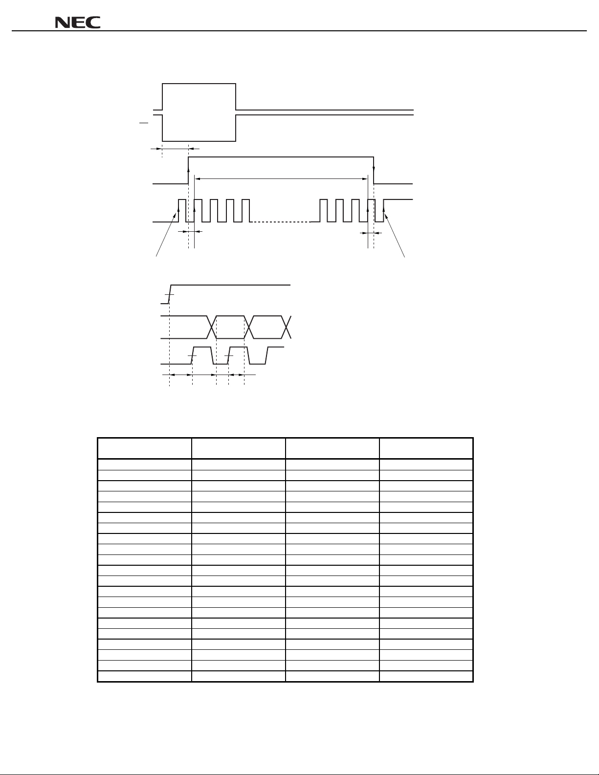
Fig 1. Delay Time of Serial Data
D
V
V
D
(VD-LATCH)
t
LATCH
104 clocks (8 bits × 13 bytes)
SCLK
t
t
(SCLK-LATCH)
Ignored because LATCH is at low level
LATCH
SDATA
SCLK
50%
50%
t
(SCLK-LATCH)
D1 D2
50%
t
setup
D3
t
hold
Table 1. Chopping Frequency (3rd byte D5 to D0 bit data, f
Input data
D5 to D0 bit
Chopping frequency
(kHz)
(SCLK-LATCH)
Ignored because LATCH is at low level
= 4.5 MHz) Typical Value
CLK
Input data
D5 to D0 bit
001000 35.71 011101 132.35
001001 40.18 011110 132.35
001010 45.00 011111 140.63
001011 50.00 100000 140.63
001100 53.57 100001 150.00
001101 59.21 100010 150.00
001110 62.50 100011 160.71
001111 68.18 100100 160.71
010000 72.58 100101 160.71
010001 77.59 100110 173.08
010010 80.36 100111 173.08
010011 86.54 101000 173.08
010100 90.00 101001 187.50
010101 93.75 101010 187.50
010110 97.83 101011 187.50
010111 102.27 101100 204.55
011000 107.14 101101 204.55
011001 112.50 101110 204.55
011010 118.42 101111 204.55
011011 118.42 110000 225.00
011100 125.00
Chopping frequency
(kHz)
When data are less than 7 (000111), PWM chopping doesn’t do it, and output pulse doesn’t occur.
Note
When data are beyond 49, PWM chopping frequency becomes a 225 kHz fixation.
4
Data Sheet S14188EJ1V0DS00

Table 2. Relation Between Rotation Angle, Phase Current, and Vector Quantity
(64-DIVISION MICRO STEP)
(Value of
PD16879 for reference)
µ
A phase current B phase current Vector quantitySTEP Rotation angle (θ)
MIN. TYP. MAX. MIN. TYP. MAX. TYP.
00
θ
1 5.6 2.5 9.8 17.0
θ
2 11.3 12.4 19.5 26.5 93.2 98.1 103 100
θ
3 16.9 22.1 29.1 36.1 90.7 95.7 100.7 100.02
θ
4 22.5 31.3 38.3 45.3 87.4 92.4 97.4 100.02
θ
5 28.1 40.1 47.1 54.1 83.2 88.2 93.2 99.99
θ
6 33.8 48.6 55.6 62.6 78.1 83.1 88.1 99.98
θ
7 39.4 58.4 63.4 68.4 72.3 77.3 82.3 99.97
θ
8 45 65.7 70.7 75.7 65.7 70.7 75.7 99.98
θ
9 50.6 72.3 77.3 82.3 58.4 63.4 68.4 99.97
θ
10 56.3 78.1 83.1 88.1 48.6 55.6 62.6 99.98
θ
11 61.9 83.2 88.2 93.2 40.1 47.1 54.1 99.99
θ
12 67.5 87.4 92.4 97.4 31.3 38.3 45.3 100.02
θ
13 73.1 90.7 95.7 100.7 22.1 29.1 36.1 100.02
θ
14 78.8 93.2 98.1 103 12.4 19.5 26.5 100
θ
15 84.4
θ
16 90
θ
−
−
−
0
100
100
−−
−
−
−−
2.5 9.8 17.0 100.48
100
100
0
−
−
−
µµµµ
PD16879
100
100.48
100
Remark
These data do not indicate guaranteed values.
Data Sheet S14188EJ1V0DS00
5

PIN CONFIGURATION
µµµµ
PD16879
10
11
12
13
14
15
16
17
18
19
1
LGND
2
3
4
5
6
7
8
9
C
FIL
FIL
FIL
FIL
V
V
V
D
FB
D
V
C
FB
C
OSC
A
B
C
D
REF
DD
M3
2
D
1
M4
2
C
1
EXP0
EXP1
REFsel
V
RESET
OSC
OSC
SCLK
SDATA
LATCH
FB
V
FB
V
EXT
EXT
PGND
OUT
V
V
38
37
IN
36
35
34
33
D
32
D
31
B
2
30
B
29
B
1
28
M2
27
A
2
26
A
25
A
1
24
M1
23
β
22
21
α
20
6
Data Sheet S14188EJ1V0DS00

PIN FUNCTION
Package: 38-pin plastic shrink SOP
Pin Pi n name Pin function
1 LGND Control circuit GND pi n
2C
3FIL
4FIL
5FIL
6FIL
7V
8VDDControl circuit supply voltage input pin
9VM3Output circuit supply voltage input pin
10 D
11 FB
12 D
13 V
14 C
15 FB
16 C
17 EXP0 External extension pin (open drain)
18 EXP1 External extension pin (open drain)
19 V
20 P GND Out put circuit GND pin
21 EXT
22 EXT
23 V
24 A
25 FB
26 A
27 V
28 B
29 FB
30 B
31 V
32 V
33 LATCH LATCH signal input pin
34 SDATA Serial data input pi n
35 SCLK Serial clock input pin (4.5 MHz typ)
36 OSC
37 OSC
38 RESET Reset signal input pin
OSC
A
B
C
D
REF
2
D
1
M4
2
C
1
REFsel
αα
ββ
M1
1
A
2
M2
1
B
2
D
D
IN
OUT
Chopping capacitor connection pi n
1 ch filter capacitor connection pin
α
2 ch filter capacitor connection pin
α
1 ch filter capacitor connection pin
β
2 ch filter capacitor connection pin
β
Reference voltage input pin (250 mV typ)
2 ch output pin
β
2 ch sense resistor connection pin
β
2 ch output pin
β
Output circuit supply voltage input pin
1 ch output pin
β
1 ch sense resistor connection pin
β
1 ch ouptut pin
β
Reference voltage select pi n
ch logic circuit m oni tor pin
ch logic circuit m oni tor pin
Output circuit supply voltage input pin
1 ch output pin
α
1 ch sense resistor connection pin
α
1 ch output pin
α
Output circuit supply voltage input pin
2 ch output pin
α
2 ch sense resistor connection pin
α
2 ch output pin
α
Video sync signal input pi n
Video sync signal input pi n
Original oscillation input pin (4.5 MHz typ)
Original oscillation output pin
Note 2
Note 2
Note 1
Note 1
µµµµ
PD16879
Remark
Notes 1.
M
Plural terminal (V
) is not only 1 terminal and connect all terminals.
A standard voltage to use is chosen.
REFsel
V
: High level using external input V
REFsel
V
: Low level using internal reference voltage (V
Input the video sync singnal to VD pin or VD pin. A free terminal is to do the following treatment.
2.
REF
REF
pin fixed GND level)
When input VD: VD pin connect to VDD pin.
When input VD: VD pin connect to GND pin.
Data Sheet S14188EJ1V0DS00
7

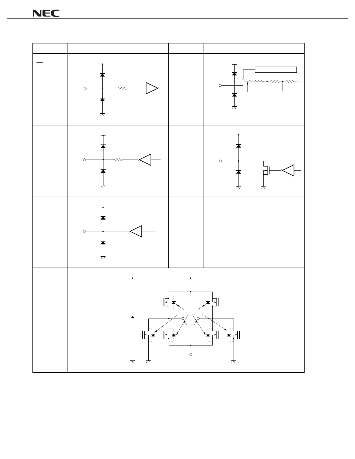
I/O PIN EQUIVALENT CIRCUIT
Pin name Equival ent circuit Pin name Equivalent circuit
µµµµ
PD16879
D
V
D
V
LATCH
SDATA
SCLK
IN
OSC
RESET
REFsel
V
OUT
OSC
α
EXT
β
EXT
A
FIL
B
FIL
C
FIL
D
FIL
PAD
PAD
PAD
REF
V
DD
V
V
DD
Internal 250 mV
PAD
V
REFsel
EXP0
V
V
DD
EXP1
DD
PAD
V
DD
A1, A
B1, B
C1, C
D1, D
Buffer
2
2
2
2
VM
Parasitic diodes
PAD
FB
8
Data Sheet S14188EJ1V0DS00

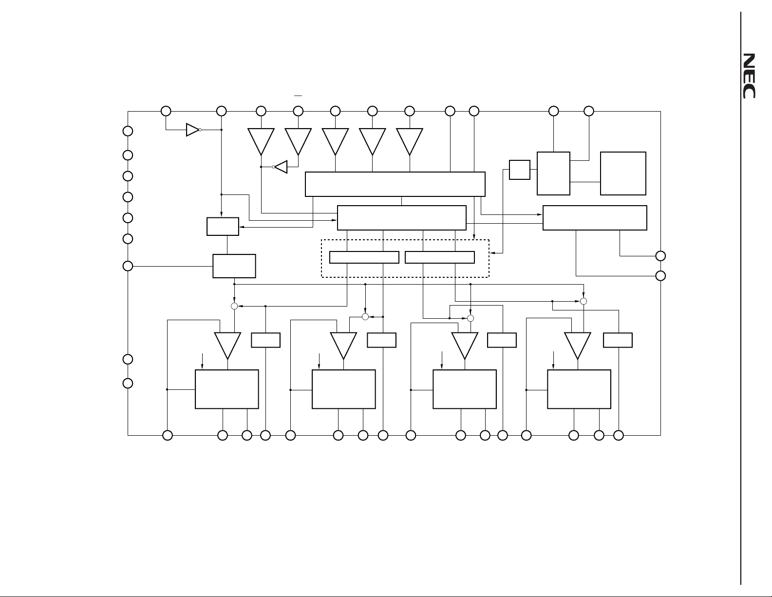
BLOCK DIAGRAM
Remark
OSC
OSC
IN
OUT
V
D
V
D
SCLK
SDATA LATCH
EXP0
EXP1
V
REFsel
V
REF
Plural terminal (V
M
) is not only 1 terminal and connect all terminals.
RESET
V
V
V
V
36
37
32 31 35 34 33
38
8
DD
M1
23
SERIAL-PARARELLE DECODER
M2
27
9
M3
PULSE GENERATER
17
18
× 2
19
7
Vref
select
EXTOUT SELECTOR
250 mV
B.G.R
1/N
V
Data Sheet S14188EJ1V0DS00
C
OSC
LGND
PGND
13
M4
21
22
FILTER
α
CURRENT SET
2
V
OSC
+
+
–
M
FILTER
CURRENT SET
–
V
M
+
+
β
+
+
+
–
V
M
FILTER
V
+
–
M
FILTER
EXT
EXT
EXT
α
β
1
20
H BRIDGE
α
1ch
H BRIDGE
2ch
α
H BRIDGE
β
1ch
H BRIDGE
2ch
β
25 24 26
A
FB
A
1
3
29
FIL
A
A
2
FB
B
28
30 4
B
1
FIL
B
2
15 16 14 5
B
FB
C
C2FIL
C
1
11
C
FB
D
12
D
1
6
10
FIL
D
D
2
µµ
µ
µ
PD16879
9

10
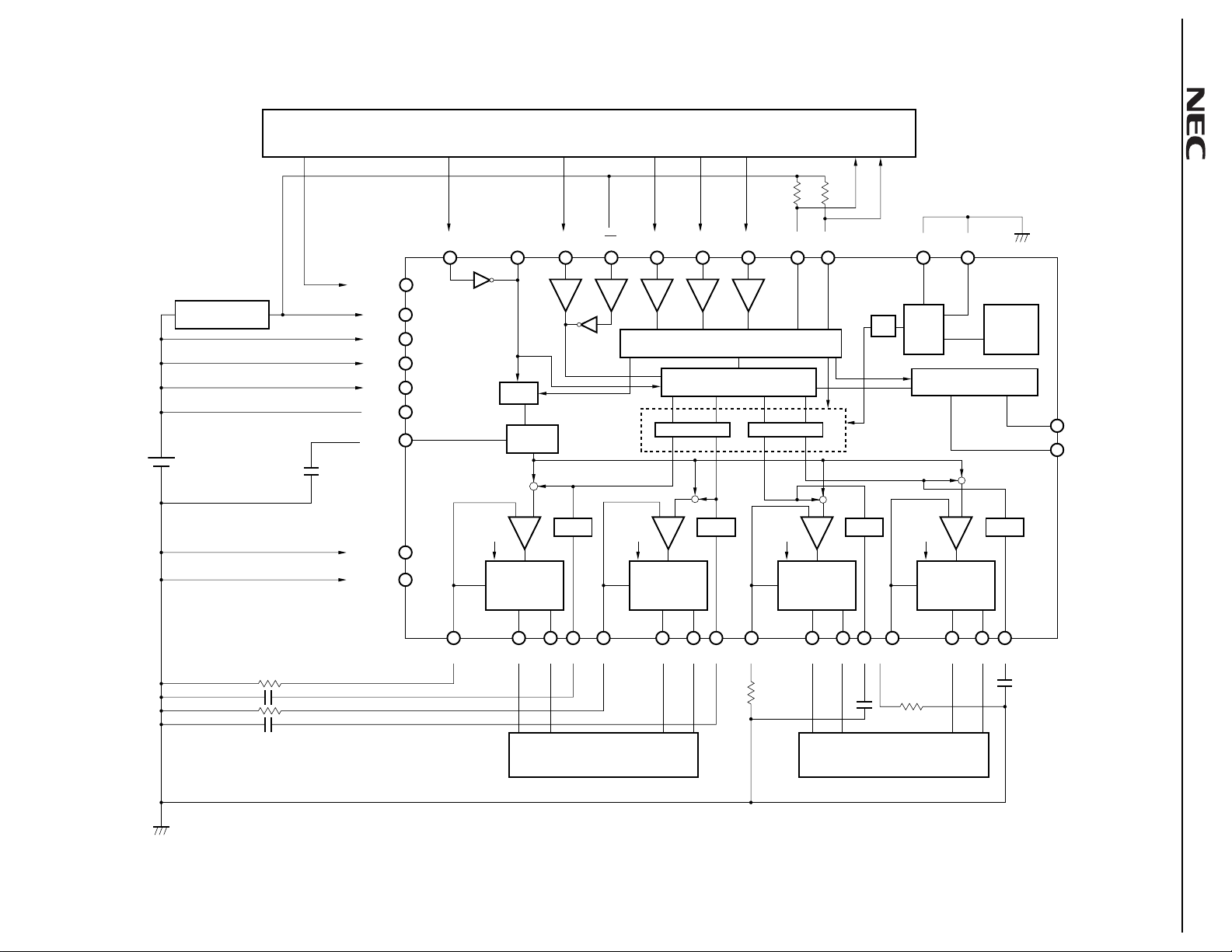
EXAMPLE OF STANDARD CONNECTION
CPU
100 kΩ × 2
4.5 MHz TYP.
V
D
V
D
IN
OSC
OSC
36
V
V
V
V
V
OSC
38
DD
8
M1
23
27
M2
M3
9
13
M4
2
RESET
REGULATOR
Data Sheet S14188EJ1V0DS00
2.7 V to 5.5 V
C
OUT
37 32 31 35 34 33
1/N
OSC
SCLK
SDATA LATCH
SERIAL-PARALLELE DECODER
PULSE GENERATOR
CURRENT SET CURRENT SET
α
EXP0
EXP1
17
β
18
BATTERY
4.0 V to 11 V
68 pF
LGND
PGND
1
20
25
+
–
V
M
H BRIDGE
1ch
α
24
+
+
+
FILTER
–
V
M
FILTER
V
H BRIDGE
1ch
α
26
30
3
29
28
4
15 16
+
+
–
M
H BRIDGE
1ch
β
FILTER
14
Using internal reference
V
REFselVREF
19
7
× 2
Vref
select
250 mV
B.G.R
EXTOUT SELECTOR
+
+
–
V
M
FILTER
H BRIDGE
1ch
β
511 12106
21
22
EXT
EXT
α
β
6.8 Ω × 2
1000 pF × 2
FB
C
A
1
A
2
FIL
A
FB
A
B
B2FIL
B
1
B
FB
C
6.8 Ω
2
FILCFB
C
1
D
6.8 Ω
D1D2FIL
D
1000 pF
1000 pF
µµ
µ
MOTOR 1
MOTOR 2
µ
PD16879
 Loading...