


µµµµ
查询UPD16878供应商
MONOLITHIC QUAD H BRIDGE DRIVER CIRCUIT
DESCRIPTION
The µPD16878 is a monolithic quad H bridge driver IC that employs a CMOS control circuit and a MOS FET
output circuit. Because it uses MOS FETs in its output stage, this driver IC consumes less power than conventional
driver ICs that use bipolar transistors.
Because the µPD16878 controls a motor by inputting serial data, its package has been shrunk and the number of
pins reduced. As a result, the performance of the application set can be improved and the size of the set has been
reduced.
The µPD16878 employs a current-controlled 64-step micro step driving method that drives stepper motor with low
vibration.
The µPD16878 is housed in a 38-pin plastic shrink SOP to contribute to the miniaturization of the application set.
The µPD16878 can simultaneously drive two stepper motors and is ideal for the mechanisms of camcorders.
DATA SHEET
MOS INTEGRATED CIRCUIT
PD16878
FEATURES
• Four H bridge circuits employing power MOS FETs
• Current-controlled 64-step micro step driving
• Motor control by serial data (8 bytes x 8 bits) (original oscillation: 4-MHz input)
Data is input with the LSB first.
EVR reference setting voltage: 100 to 250 mV (@VREF
Chopping frequency: 32 to 124 kHz ... 5-bit data input (4-kHz step)
Original oscillation division or internal oscillation selectable
Number of pulses in 1 VD: 0 to 126 pulses ... 6 bits + 2-bit data input (2 pulses/step)
Step cycle: 0.25 to 8191.75 µs ... 15-bit data input (0.25- µs step)
• 3-V power supply. Minimum operating voltage: 2.7 V (MIN.)
• Low current consumption IDD: 3.0 mA (MAX.), IDD
• 38-pin plastic shrink SOP (7.62 mm (300))
ORDERING INFORMATION
Part number Package
PD16878GS-BGG 38-pin plastic shrink SOP (7.62 mm (300))
µ
= 250 mV) ... 4-bit data input (10-mV step)
: 100 µA (MAX.), I
(RESET)
MO(RESET)
: 1.0 µA (MAX.)
The information in this document is subject to change without notice. Before using this document, please
confirm that this is the latest version.
Not all devices/types available in every country. Please check with local NEC representative for
availability and additional information.
Document No. S15974EJ1V0DS00 (1st edition)
Date Published February 2002 N CP(K)
Printed in Japan
©
2002
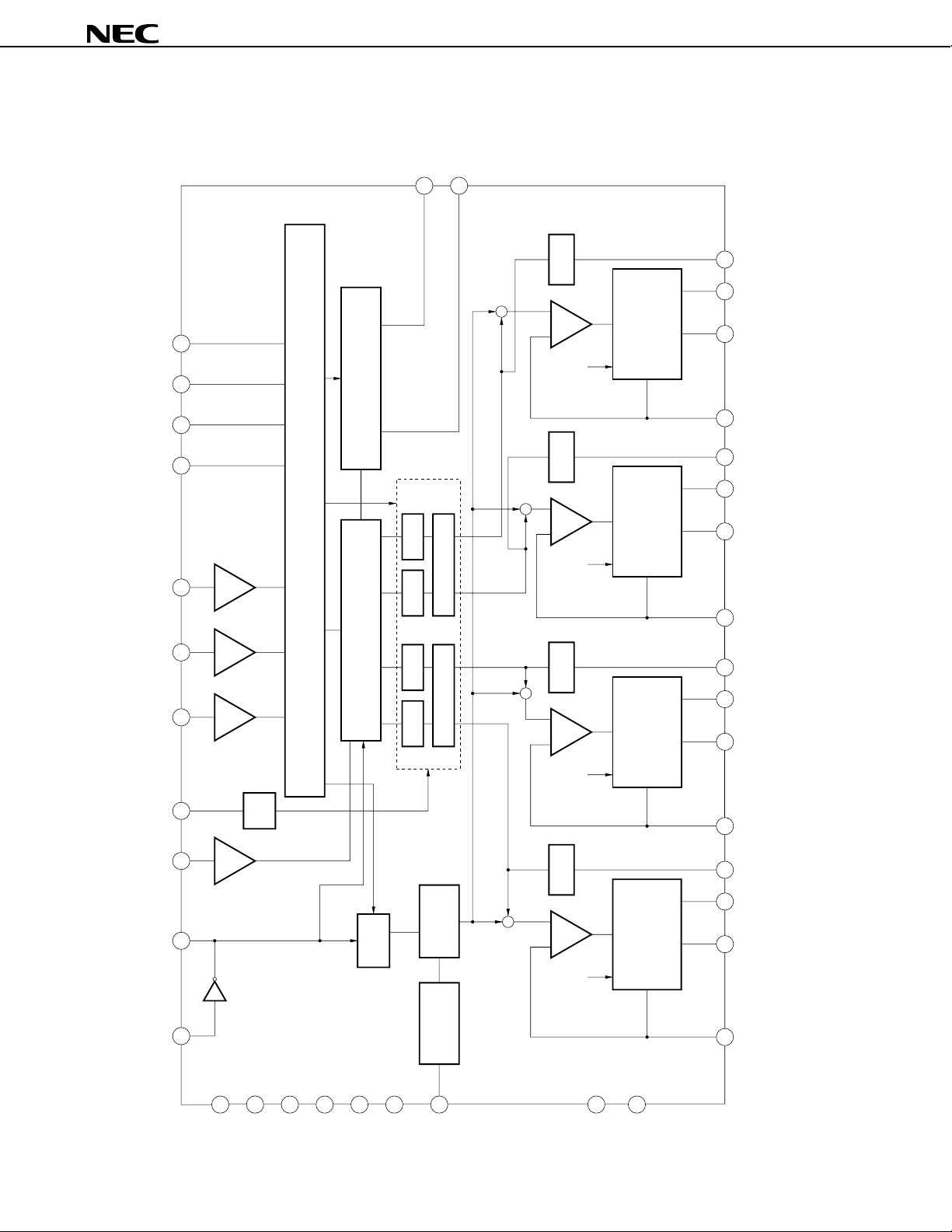
BLOCK DIAGRAM
EXP0 EXP1 EXP2 EXP3
α
β
EXT
EXT
31
22
EXTOUT SELECTOR
β
µµµµ
PD16878
D
FILTERFILTERFILTERFILTER
+
2ch
–+
M
V
β
H BRIDGE
10125141643028326
FIL
2
D
1
D
D
FB
C
FIL
2
+
–+
M
V
1ch
β
H BRIDGE
C
1
C
SCLK SDATA LATCH
REF
V
D
V
OUT
OSC
IN
OSC
SERIAL-PARARELLE DECODER
EVR1 EVR2
CURRENT SET
C
FB
x 2
α
PULSE GENERATER
EVR2
EVR1
CURRENT SET
+
–+
M
V
2ch
α
H BRIDGE
B
FIL
2
B
1
B
B
FB
A
FIL
2
A
OSC
1/N
37 36 32 7 35 34 33 17 18 19 21
SELECTOR
+
–+
M
V
1ch
α
H BRIDGE
1
A
25 24 29 15 11 6
A
FB
38
8
23
27
9
13
2
DD
VM1VM2VM3V
V
M4
OSC
C
RESET
2
Data Sheet S15974EJ1V0DS
1
LGND
20
PGND
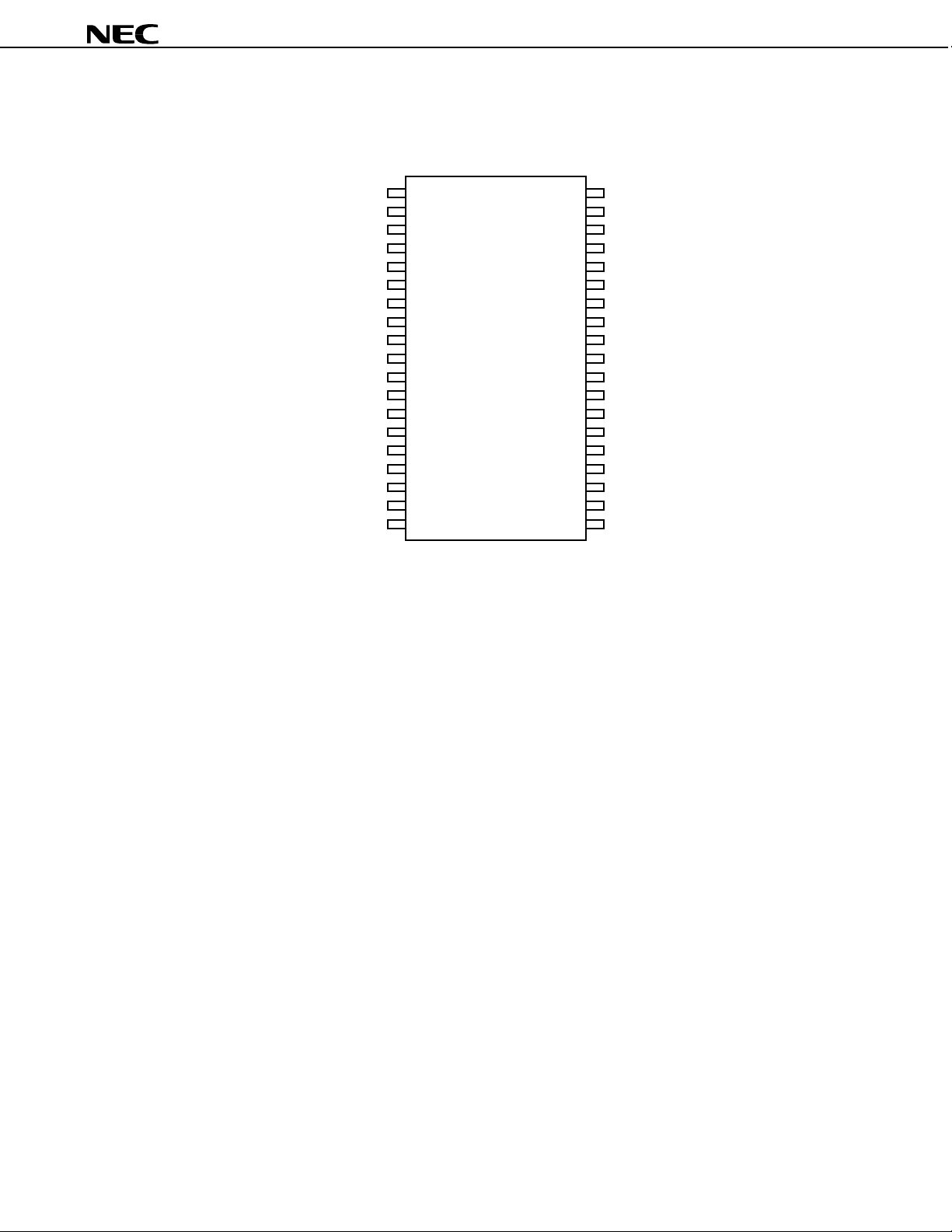
PIN CONFIGURATION
38-pin plastic shrink SOP (7.62 mm (300))
10
11
12
13
14
15
16
17
18
19
µµµµ
PD16878
1
LGND
2
C
OSC
3
FIL
A
4
FIL
B
5
FIL
C
6
FIL
D
7
V
REF
8
V
DD
V
M3
9
D
2
FB
D
D
1
V
M4
C
2
FB
C
C
1
EXP0
EXP1
EXP2
RESET
OSC
OSC
SCLK
SDATA
LATCH
EXT
FB
FB
EXT
EXP3
PGND
V
V
OUT
V
B
B
A
A
38
37
IN
36
35
34
33
D
32
β
31
2
30
B
29
1
28
M2
27
2
26
A
25
1
24
M1
23
α
22
21
20
Data Sheet S15974EJ1V0DS
3

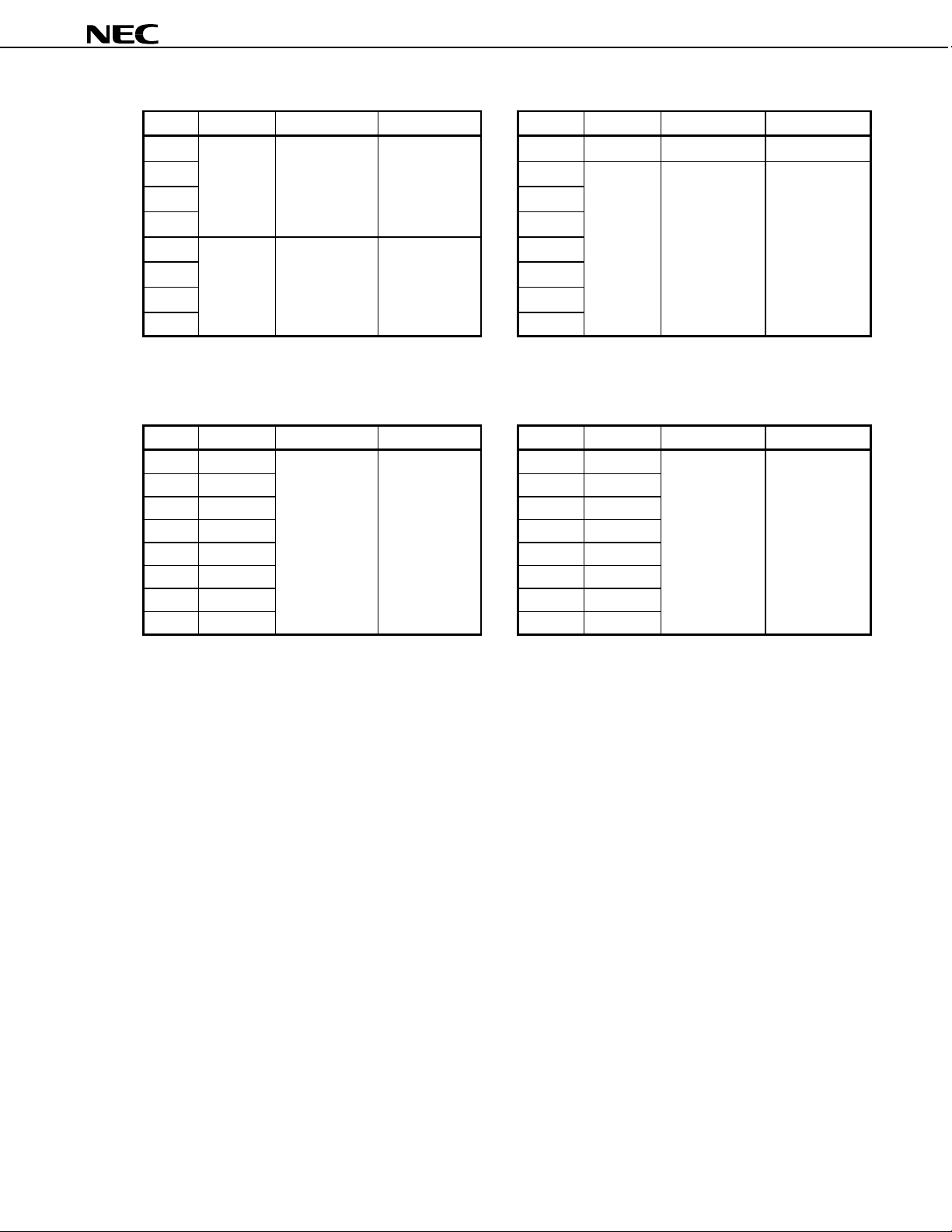
1. PIN FUNCTIONS
Pin No. Symbol Function
1 LGND Control circuit GND pin
2C
3FIL
4FIL
5FIL
6FIL
7V
8V
9V
10 D
11 FB
12 D
13 V
14 C
15 FB
16 C
OSC
A
B
C
D
REF
DD
M3
2
D
1
M4
2
C
1
17 EXP0 Output monitor pin (open drain)
18 EXP1 Output monitor pin (open drain)
19 EXP2 Output monitor pin (open drain)
20 PGND Power circuit GND pin
21 EXP3 Output monitor pin (open drain)
22 EXT
23 V
24 A
25 FB
26 A
27 V
28 B
29 FB
30 B
31 EXT
32 V
α
M1
1
A
2
M2
1
B
2
β
D
33 LATCH Latch signal input pin
34 SDATA Serial data input pin
35 SCLK Serial clock input pin
36 OSC
37 OSC
IN
OUT
38 RESET Reset signal output pin
Chopping capacitor connection pin
α
1-ch filter capacitor connection pin (1000 pF TYP.)
α
2-ch filter capacitor connection pin (1000 pF TYP.)
β
1-ch filter capacitor connection pin (1000 pF TYP.)
β
2-ch filter capacitor connection pin (1000 pF TYP.)
Reference voltage input pin (250 mV TYP.)
Control circuit supply voltage input pin
Output circuit supply voltage input pin
β
2-ch output pin
β
2-ch sense resistor connection pin
β
2-ch output pin
Output circuit supply voltage connection pin
β
1-ch output pin
β
1-ch sense resistor connection pin
β
1-ch output pin
Logic circuit monitor pin
Output circuit supply voltage input pin
α
1-ch output pin
α
1-ch sense resistor connection pin
α
1-ch output pin
Output circuit supply voltage input pin
α
2-ch output pin
α
2-ch sense resistor connection pin
α
2-ch output pin
Logic circuit monitor pin
Video sync signal input pin
Original oscillation input pin (4 MHz TYP.)
Original oscillation output pin
µµµµ
PD16878
4
Data Sheet S15974EJ1V0DS
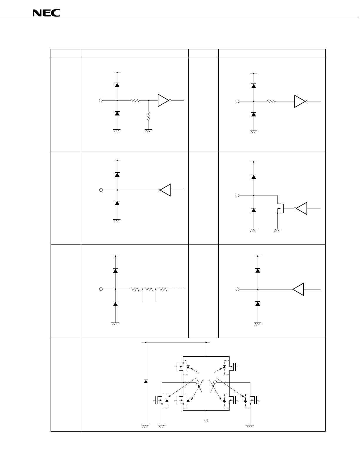
2. I/O PIN EQUIVALENT CIRCUIT
Pin Name Equivalent Circuit Pin Name Equivalent Circuit
DD
V
DD
LATCH
SDATA
SCLK
Pad
V
OSC
IN
Pad
RESET
Pull-down
resistor (125 Ω)
V
DD
V
DD
DD
V
µµµµ
PD16878
OSC
EXT
EXT
V
REF
α
β
OUT
Pad
Pad
EXP0
EXP1
Pad
EXP2
EXP3
V
DD
FIL
A
FIL
FIL
FIL
B
C
D
Pad
V
M
DD
V
Buffer
A1, A
B1, B
C1, C
D1, D
2
2
2
2
Parasitic diodes
Pad
FB
Data Sheet S15974EJ1V0DS
5
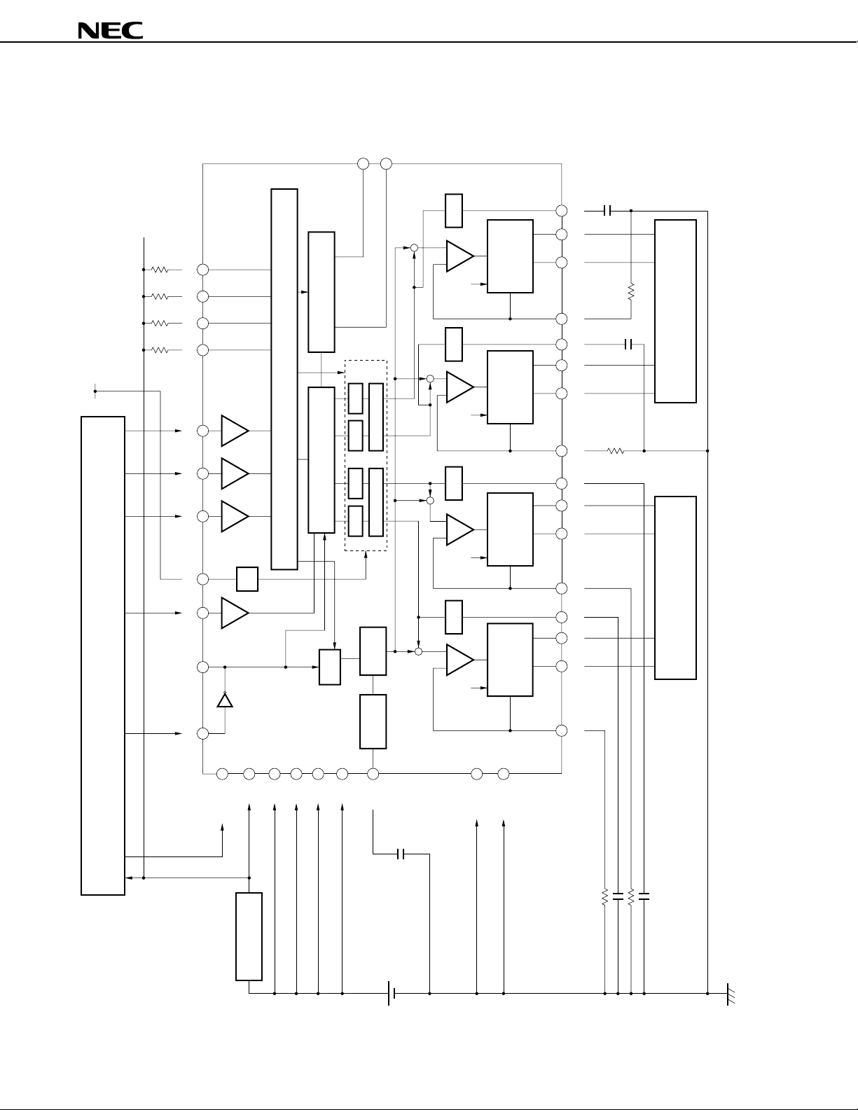
3. EXAMPLE OF STANDARD CONNECTION
α
EXT
100 kΩ x 4
EXTOUT SELECTOR
: 64 kHz
OSC
250 mV
EVR : 1010
f
CPU
EXP0 EXP1EXP2 EXP3
SCLK SDATA LATCH
REF
V
D
V
OUT
OSC
EVR1 EVR2
SERIAL-PARARELLE DECODER
EVR2
PULSE GENERATER
EVR1
x2
1/N
β
EXT
+
+
β
CURRENT SET
α
+
CURRENT SET
OSC
+
FILTERFILTERFILTERFILTER
– +
M
V
– +
M
V
– +
M
V
– +
M
V
2ch
β
H BRIDGE
1ch
β
H BRIDGE
2ch
α
H BRIDGE
1ch
α
H BRIDGE
D
FIL
2
D
1
D
D
FB
C
FIL
2
C
1
C
C
FB
B
FIL
2
B
1
B
B
FB
A
FIL
2
A
1
A
1000 pF
6.8 Ω
6.8 Ω
1000 pF
µµµµ
PD16878
MOTOR 1 MOTOR 2
IN
OSC
SELECTOR
A
FB
4 MHz
M4
OSC
C
LGND
PGND
RESET
DD
VM1VM2VM3V
V
33 pF
3.3 V
6.8 Ω x 2
REGULATOR
6
Data Sheet S15974EJ1V0DS
BATTERY
4.8 to 11 V
1000 pF x 2
4. STANDARD CHARACTERISTICS CURVES
µµµµ
PD16878
1.4
PT vs. TA Characteristics I
1.2
(W)
T
1.0
125°C/W
0.8
0.6
0.4
Total Power Dissipation P
0.2
0
20 40 60–10 0
Ambient Temperature T
5
IDD vs. VDD Characteristics
4
(mA)
DD
3
2
pin Current I
DD
V
1
0
234
Control Circuit Supply Volage V
80 100 120
A
(°C)
TA = 25°C,
operating,
output open
56
DD
(V)
1
µ
0.8
( A)
MO (RESET)
0.6
MO (RESET)
vs. VM Characteristics
0.4
pin Current I
M
0.2
OFF V
0
468
Output Circuit Supply Voltage V
200
µ
( A)
150
DD (RESET)
DD (RESET)
vs. VDD Characteristics
I
100
50
pin Current at Reset State I
DD
V
0
234
Control Circuit Supply Volage V
TA = 25°C,
no load,
after reset
10 12
M
(V)
TA = 25°C,
after reset
56
DD
(V)
VIH/VDD, VIL/VDD vs. VDD Characteristics
1
(V)
0.8
DD
/V
IL
, V
0.6
DD
/V
IH
0.4
0.2
Input Voltage V
0
234
Control Circuit Supply Volage V
TA = 25°C
V
IH
IL
V
56
DD
(V)
60
µ
( A)
IL
/I
IH
40
20
0
High-level/Low-level Input Current I
Data Sheet S15974EJ1V0DS
IIH/IIL vs. VIN Characteristics
I
IH
I
IL
234
IN
Input Voltage V
(V)
TA = 25°C,
IIH: VIN = VDD,
I
IL
:
VIN = 0 V
56
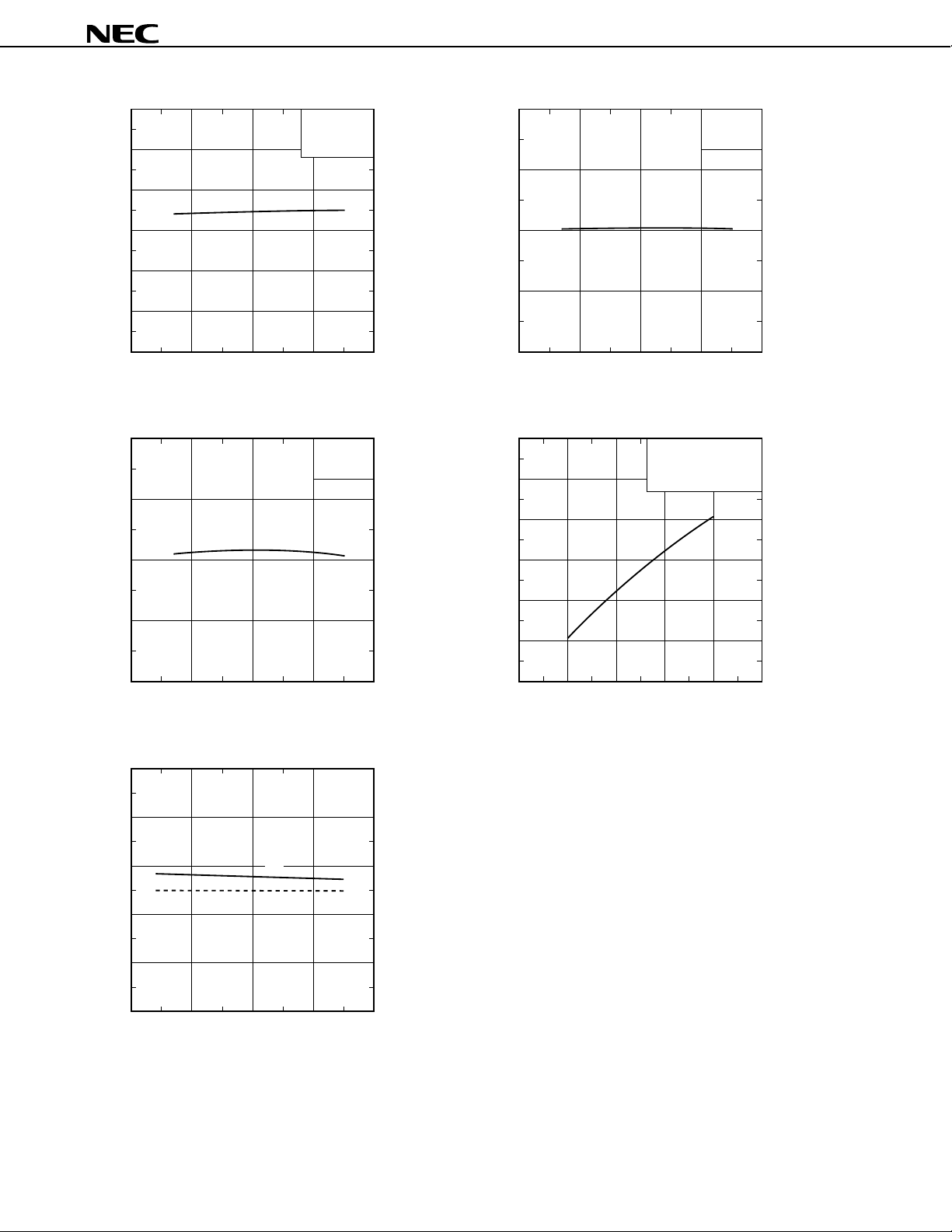
7
f
OSC
150
vs. VDD Characteristics f
140
(kHz)
130
OSC
120
110
Chopping Frequency f
100
TA = 25°C,
C
OSC
= 100 pF,
DATA: all high
6
STEP vs. VDD Characteristics
5
(kHz)
STEP
4
3
Step Frequency f
TA = 25°C,
C
OSC
= 100 pF
µµµµ
PD16878
90
23456
Control Circuit Supply Voltage V
V
REFVER
40
vs. VDD Characteristics
DD
(V)
TA = 25°C,
V
REF
= 250 mV
(mV)
30
REFVER
20
10
EVR Variable Voltage V
0
234
Control Circuit Supply Voltage V
tON, t
OFF
500
vs. VM Characteristics
56
DD
(V)
TA = 25°C,
IM = 100 mA,
C
FIL
(ns)
400
OFF
/t
ON
300
t
ON
: none
2
234
Control Circuit Supply Voltage V
I
M (MAX)
80
vs. EVR Characteristics
56
DD
(V)
TA = 25°C, VM = 6 V
(mA)
70
M (MAX)
Rs = 6.8 Ω, f
L = 25 mH/R = 100 Ω at 1 kHz
OSC
= 64 kHz,
60
50
40
30
Sine Wave Peak Output Current I
20
50 100 150 200 250 300
Reference Setting Voltage EVR (mV)
200
100
Turn-on Time, Turn-off Time t
0
468
Output Circuit Supply Voltage V
8
t
OFF
10 12
M
(V)
Data Sheet S15974EJ1V0DS
µµµµ
PD16878
5. INTERFACE (I/F) CIRCUIT DATA CONFIGURATION (f
= 4-MHz EXTERNAL CLOCK INPUT)
CLK
Input data consists of serial data (8 bytes x 8 bits).
Input serial data with the LSB first, from the 1st byte to 8th byte.
(1) Initial data (2) Standard data
<1st byte> <1st byte>
Bit Data Function Setting Bit Data Function Setting
D7 1
D6 1
D5 1
D4 0 −− D4 0 −−
D3 1 or 0 EXP3 Hi-Z or L D3 1 or 0 EXP3 Hi-Z or L
D2 1 or 0 EXP2 Hi-Z or L D2 1 or 0 EXP2 Hi-Z or L
D1 1 or 0 EXP1 Hi-Z or L D1 1 or 0 EXP1 Hi-Z or L
D0 1 or 0 EXP0 Hi-Z or L D0 1 or 0 EXP0 Hi-Z or L
HEADER DATA2
HEADER DATA1
HEADER DATA0
DATA selection
Remark Hi-Z : High impedance,
L : Low level (current sink)
D7 0
D6 0
D5 0
HEADER DATA2
HEADER DATA1
HEADER DATA0
Remark Hi-Z : High impedance,
L : Low level (current sink)
DATA selection
<2nd byte> <2nd byte>
Bit Data Function Setting Bit Data Function Setting
D7 D7 1 or 0
D6 D6 1 or 0
D5 D5
D4 D4
8-bit data
input
D3 D3
D2 D2
D1 D1
D0
Note
First Point Wait
Start point wait
s to 2.04 ms
8
µ
Setting
(1 to 255)
s
µ
∆t = 8
6-bit data
input
D0
ROTATION
α
ENABLE
α
Pulse Number
α
ch CCW/CW
α
ch ON/OFF
α
ch
α
Number of
pulses in 1 VD
Setting (0 to 63)
∆n = 2 pulses
Note Input other than “0”. Note The number of pulses can be varied in 2-pulse
steps.
Note
<3rd byte> <3rd byte>
Bit Data Function Setting Bit Data Function Setting
D7 D7
D6 D6
D5 D5
D4 D4
8-bit data
input
D3 D3
D2 D2
D1 D1
D0
Note
First Point
Magnetize Wait
Start point drive
wait
s to 2.04 ms
µ
8
Setting
(1 to 255)
s
µ
∆t = 8
D0
15-bit data
Low-order
8-bit data
input
Pulse Width
α
ch pulse
α
cycle
0.25 to 8191.75 µs
Setting
(1 to 32767)
∆t = 0.25
Note Input other than “0”.
Data Sheet S15974EJ1V0DS
s
µ
9
<4th byte> <4th byte>
Bit Data Function Setting Bit Data Function Setting
D7 1 or 0 OSCSEL
Internal/external
D6 0 - - D6
D7 1 or 0 Current Set
15-bit data
α
D5 0 - - D5
D4 D4
D3 D3
5-bit data
D2 D2
input
D1 D1
Chopping
Frequency
D0
Chopping
frequency :
32 to 124 kHz
Setting
(8 to 31)
∆f = 4 kHz
Note
D0
High-order
7-bit data
input
Pulse Width
α
Note The frequency is 0 kHz if 0 to 7 is input.
<5th byte> <5th byte>
Bit Data EXT
α
D7 0 - - D7 1 or 0
D6
D5
D4
D3
D2
D1
D0
Note 5
Note 5
Note 5
Note 5
Note 5
Note 5
Note 5
ENABLE
ROTATION
Pulse Out
FF7
FF3
Checksum
Chopping
Note1
α
Note2
α
α
α
α
Note3
Note4
Notes 1. H level : Conducts, L level : Stops
2. H level : Reverse (CCW),
EXT
ENABLE
β
ROTATION
Pulse Out
FF7
β
FF3
β
FF2
β
FF1
β
β
Note1
Bit Data Function Setting
ROTATION
β
D6 1 or 0
Note2
β
β
D5
D4
D3
D2
6-bit data
input
ENABLE
β
Pulse Number
β
D1
D0
Note The number of pulses can be varied in 2-pulse
steps.
L level : Forward (CW)
3. H level : Normal data input,
L level : Abnormal data input
4. Not output in internal oscillation mode.
5. Select one of D0 to D6 and input “1”.
If two or more of D0 to D6 are selected,
they are positively ORed for output.
µµµµ
PD16878
set2/set1
α
ch
pulse cycle :
0.25 to 8191.75 µs
Setting
(1 to 32767)
∆t = 0.25
ch CCW/CW
β
ch ON/OFF
β
β
ch
s
µ
Number of
pulses in 1 VD
Setting (1 to 63)
∆n = 2 pulses
Note
<6th byte> <6th byte>
Bit Data Function Setting Bit Data Function Setting
D7 D7
D6 D6
4-bit data
input
D5 D5
ch
α
Current Set2
D4
D3 D3
D2 D2
4-bit data
input
D1 D1
ch
α
Current Set1
D0
α
ch Output current
setting 2
EVR : 100
to 250 mV
Setting (0 to 15)
α
ch Output current
setting 1
EVR : 100
to 250 mV
Setting (0 to 15)
Note
Note
D4
D0
15-bit data
Low-order
8-bit data
input
Pulse Width
β
Note A voltage of about double EVR is output to
the FIL pin.
10
Data Sheet S15974EJ1V0DS
β
ch pulse
cycle:
0.25 to 8191.75 µs
Setting
(1 to 32767)
∆t = 0.25
s
µ
<7th byte> <7th byte>
Bit Data Function Setting Bit Data Function Setting
D7 D7 1 or 0 Current Set
D6 D6
4-bit data
input
D5 D5
ch
β
Current Set2
D4
D3 D3
D2 D2
4-bit data
input
D1 D1
ch
β
Current Set1
D0
β
ch Output
current setting 2
EVR: 100 to 250 mV
Setting (0 to 15)
ch Output
β
current setting 1
EVR: 100 to 250 mV
Setting (0 to 15)
Note
Note
D4
D0
15-bit data
High-order
7-bit data
input
Pulse Width
β
β
Note A voltage of about double EVR is output to
the FIL pin.
<8th byte> <8th byte>
Bit Data Function Setting Bit Data Function Setting
D7 1 or 0 D7 1 or 0
D6 1 or 0 D6 1 or 0
D5 1 or 0 D5 1 or 0
D4 1 or 0 D4 1 or 0
D3 1 or 0 D3 1 or 0
Checksum Checksum
D2 1 or 0 D2 1 or 0
D1 1 or 0 D1 1 or 0
D0 1 or 0
Note Data is input so that the sum of the 1st
through the 8th bytes is 00H.
Note
Checksum Checksum
D0 1 or 0
Note Data is input so that the sum of the 1st
through the 8th bytes is 00H.
µµµµ
PD16878
set2/set1
β
ch pulse
cycle:
0.25 to 8191.75 µs
Setting
(1 to 32767)
∆t = 0.25
µ
s
Note
Data Sheet S15974EJ1V0DS
11

µµµµ
PD16878
Data Configuration
Data can be input in either of two ways. Initial data can be input when the power is first applied, or standard data
can be input during normal operation. Input serial data with the LSB first, i.e., starting from the D0 bit (LSB) of the 1st
byte. Therefore, the D7 bit of the 8th byte is the most significant bit (MSB).
When inputting initial data, set a start point wait time that specifies the delay from power application to pulse
output, and the start point drive wait time. At the same time, also set a chopping frequency and a reference voltage
(EVR) that determines the output current of each channel. Because the
internal operations, the parameter to be monitored can be selected by initial data.
When inputting standard data, input the rotation direction of each channel, the number of pulses, and the data for
the pulse cycle.
Initial data or standard data is selected by using bits D5 to D7 of the 1st byte (see Table 5-1).
Table 5-1. Data Selection Mode (1st byte)
D7 D6 D5 Data type
1 1 1 Initial data
0 0 0 Standard data
Remark If the high-order three bits are high, the initial data is selected;
if they are low, the standard data is selected.
Data other than (0, 0, 0) and (1, 1, 1) must not be input.
PD16878 has an EXT pin for monitoring the
µ
Input the serial data during start point wait time.
Details of Data Configuration
How to input initial data and standard data is described below.
(1) Initial data input
<1st byte>
The 1st byte specifies the type of data (initial data or standard data) and determines the presence or absence of
the EXP pin output. Bits D5 to D7 of this byte specify the type of data as shown in Table 5-1, while bits D0 to D3
select the EXP output (open drain).
Table 5-2. 1st Byte Data Configuration
Bit D7D6D5D4D3D2D1D0
Data 1 1 1 0 0 or 1 0 or 1 0 or 1 0 or 1
The EXP pin goes low (current sink) when the input data is “0”, and high (high impedance state) when the input
data is “1”. Pull this pin up to V
for use. Input “0” to bit D4.
DD
12
Data Sheet S15974EJ1V0DS

µµµµ
PD16878
<2nd byte>
The 2nd byte specifies the delay between data being read and data being output. This delay is called the start up
wait time, and the motor can be driven from that point at which the start up wait time is “0”. This time is counted at the
rising edge of VD. The start up wait time can be set to 2.04 ms (when a 4-MHz clock is input), and can be fine-tuned
by means of 8-bit division (8-µs step: with 4-MHz clock). The start up wait time is set to 2.04 ms when all the bits of
the 2nd byte are set to “1”.
Caution Always input data other than “0” to this byte because the start up wait time is necessary for
latching data. If “0” is input to this byte, data cannot be updated. Transfer standard data during the
start up wait time.
<3rd byte>
The 3rd byte specifies the delay between the start point wait time being cleared and the output pulse being
generated. This time is called the start up drive wait time, and the output pulse is generated from the point at which
the start up drive wait time reaches “0”. The start up drive wait time is counted at the falling edge of the start up wait
time. The start up drive wait time can be set to 2.04 ms (with 4-MHz clock) and can be fine-tuned by means of 8-bit
division (8 µs step: with 4-MHz clock). The start up drive wait time is set to 2.04 ms when all the bits of the 3rd byte
are “1”.
Caution Always input data other than “0” to this byte because the start up drive wait time is necessary for
latching data. If “0” is input to this byte, data cannot be updated.
<4th byte>
The 4th byte selects a chopping frequency by using 5-bit data. It also selects whether the chopping frequency is
created by dividing the original oscillation (external clock) or whether the internal oscillator is used. The chopping
frequency is selected by bits D0 to D4. Bit D7 specifies the method used to create the chopping frequency. When this
bit is “0”, the original oscillation (external clock input to OSCIN) is used; when it is “1”, the internal oscillator is used.
Bits D5 and D6 are fixed to “0”.
The chopping signal is output after the initial data has been input and the first standard data has been latched
(see Timing Chart).
Table 5-3. 4th Byte Data Configuration (Initial data)
Bit D7D6D5D4D3D2D1D0
Data 0 or 1 0 0 0 or 1 0 or 1 0 or 1 0 or 1 0 or 1
The chopping frequency is set to 0 kHz and to a value in the range of 32 to 124 kHz (in 4-kHz steps), as follows.
Although the chopping frequency is set by 5 bits of data, it is internally configured using 7-bit data (with the low-
order 2 bits fixed to 0).
Data Sheet S15974EJ1V0DS
13

µµµµ
PD16878
BitD7D6D5D4D3D2D1 D0
Data0 or 1000000 0
Bit D7D6D5D4D3D2D1D0
Data0 or 1000011 1
Bit D7D6D5D4D3D2D1D0
Data 0 or 1 0 0 0 1 0 0 0
Bit D7D6D5D4D3D2D1D0
Data0 or 1000100 1
Bit D7D6D5D4D3D2D1D0
Data0 or 1001111 1
f
= 0 kHz
OSC
f
= 0 kHz
OSC
f
= 32 kHz
OSC
f
= 36 kHz
OSC
f
= 124 kHz
OSC
<5th byte>
The 5th byte selects a parameter to be output to the EXT pin (logic operation monitor pin). Input data to bits D0 to
D6 of this byte. Bit D7 is fixed to “0”.
There are two EXT pins. EXT
α
indicates the operating status of α ch, and EXTβ indicates that of β ch. The
relationship between each bit and each EXT pin is as shown in Table 5-4.
Table 5-4. 5th Byte Data Configuration (Initial data)
Bit Data EXT
D7 0 Not used Not used
D6 0 or 1 ENABLE
D5 0 or 1 ROTATION
D4 0 or 1 PULSEOUT
D3 0 or 1 FF7
D2 0 or 1 FF3
D1 0 or 1 CHECKSUM FF2
D0 0 or 1 CHOPPING FF1
α
α
α
α
α
α
ENABLE
ROTATION
PULSEOUT
FF7
β
FF3
β
β
β
The checksum bit is cleared to “0” in the event of an error. Normally, it is “1”.
If two or more signals that output signals to EXT
α
and EXTβ are selected, they are positively ORed for output.
Caution The CHOPPING signal is not output in internal oscillation mode.
EXT
β
β
β
β
14
Data Sheet S15974EJ1V0DS

µµµµ
PD16878
Remark The meanings of the symbols listed in Table 5-4 are as follows:
ENABLE : Output setting (H : Conducts, L : Stops)
ROTATION : Rotation direction (H : Reverse (CCW), L : Forward (CW))
PULSEOUT : Output pulse signal
FF7 : Presence/absence of pulse in LATCH cycle (Outputs H level if output pulse information exists in
standard data.)
FF3 : Pulse gate (output while pulse exists)
FF2 : Outputs H level during start up wait time + start up drive wait time
FF1 : Outputs H level during start up wait time
CHECKSUM : Checksum output (H : when normal data is transmitted,
L : when abnormal data is transmitted)
CHOPPING : Chopping wave output (in original oscillation mode only)
<6th byte>
The 6th byte sets the peak output current value of α ch. The output current is determined by the EVR reference
voltage.
The 250-mV (TYP.) voltage input from an external source to the VREF
pin is internally doubled and input to a 4-bit
D/A converter. By dividing this voltage by 4-bit data, an EVR reference voltage can be set inside the IC within the
range of 200 to 500 mV, in units of 20 mV.
The µPD16878 can set two values of the EVR reference voltage in advance. This is done by using bits D0 to D3
or D4 to D7. Which of the two EVR reference voltage values is to be used is specified by the CURRENT SET bit in
the standard data.
If all the bits of the 6th byte are “0”, the EVR reference voltage of 200 mV is selected; if they are “1”, the EVR
reference voltage of 500 mV is selected.
Table 5-5. 6th Byte Data Configuration (Initial data)
Bit D7D6D5D4D3D2D1D0
Data 0 or 1 0 or 1 0 or 1 0 or 1 0 or 1 0 or 1 0 or 1 0 or 1
Remark Bits D4 to D7 : Reference voltage 2 (EVR
Bits D0 to D3 : Reference voltage 1 (EVR
)
α
2
)
α
1
<7th byte>
The 7th byte specifies the peak output current value of
β
ch. The output current is determined by the EVR
reference voltage.
The 250-mV (TYP.) voltage input from an external source to the VREF
pin is internally doubled and input to a 4-bit
D/A converter. By dividing this voltage by 4-bit data, an EVR reference voltage can be set inside the IC within a range
of 200 to 500 mV, in units of 20 mV.
The µPD16878 can set two values of the EVR reference voltage in advance. This is done using bits D0 to D3 or
D4 to D7. Which of the two EVR reference voltage values is to be used is specified by the CURRENT SET bit in the
standard data.
If all the bits of the 7th byte are “0”, the EVR reference voltage of 200 mV is selected; if they are “1”, the EVR
reference voltage of 500 mV is selected.
Data Sheet S15974EJ1V0DS
15
µµµµ
Table 5-6. 7th Byte Data Configuration (Initial data)
Bit D7D6D5D4D3D2D1D0
Data 0 or 1 0 or 1 0 or 1 0 or 1 0 or 1 0 or 1 0 or 1 0 or 1
Remark Bits D4 to D7 : Reference voltage 2 (EVR
Bits D0 to D3 : Reference voltage 1 (EVR
<8th byte>
The 8th byte is checksum data. Normally, the sum of the 8-byte data is 00H.
If the sum is not 00H because data transmission is abnormal, the stepping operation is inhibited and the
checksum output pin (EXT pin) is kept “L”.
(2) Standard data input
<1st byte>
The 1st byte specifies the type of data and whether the EXP pin output is used, such as when the initial data is
input.
)
β
2
)
β
1
PD16878
Table 5-7. 1st Byte Data Configuration
Bit D7D6D5D4D3D2D1D0
Data 1 1 1 0 0 or 1 0 or 1 0 or 1 0 or 1
The EXP pin goes low (current sink) when the input data is “0”, and high (high impedance state) when the input
data is “1”. Input “0” to bit D4.
<2nd byte>
The 2nd byte specifies the rotation direction of the
pulses (126 pulses MAX.) during the 1VD
period (in 1 cycle of FF2) of the
α
channel, enables output of the α channel, and the number of
α
channel.
Bit D7 is used to specify the rotation direction. The rotation is in the forward direction (CW mode) when this bit is
“0”; it is in the reverse direction (CCW mode) when the bit is “1”.
Bit D6 is used to enable the output of the α channel. The α channel enters the high impedance state when this bit
is “0”; it is in conduction mode when the bit is “1”.
The number of pulses is set by bits D0 to D5. It is set by 6 bits in terms of software. However, the actual circuit
uses an 8-bit counter with the low-order two bits fixed to “0”. Therefore, the number of pulses that is actually
generated during start up wait time + start up drive wait (FF2) cycle is the number of pulses input x 2. The number of
pulses can be set to a value in the range of 0 to 126, in units of 2 pulses.
16
Data Sheet S15974EJ1V0DS

µµµµ
PD16878
Table 5-8. 2nd Byte Data Configuration (Standard data)
Bit D7D6D5D4D3D2D1D0
Data 0 or 1 0 or 1 0 or 1 0 or 1 0 or 1 0 or 1 0 or 1 0 or 1
Rotation direction ENABLE Number of pulses
<3rd and 4th bytes>
The 3rd and 4th bytes select the pulse cycle of the
the initial mode, is to be used (CURRENT SET
α
α
channel and which of the two reference voltages, created in
).
The pulse cycle is specified using 15 bits : bits D0 (least significant bit) to D7 of the 3rd byte, and bits D0 to D6
(most significant bit) of the 4th byte. The pulse cycle can be set to a value in the range of 0.25 to 8191.75 µs in units
of 0.25 µs (with a 4-MHz clock).
CURRENT SET
α
is specified by bit D7 of the 4th byte. When this bit is “0”, reference voltage 1 (EVR
selected; when it is “1”, reference voltage 2 (EVR
) is selected. For further information, refer to the description of the
α
2
) is
α
1
6th byte of the initial data.
Table 5-9. 4th Byte Data Configuration (Standard data) Table 5-10. 3rd Byte Data Configuration (Standard data)
Bit D7D6D5D4D3D2D1D0 D7D6D5D4D3D2D1D0
Data
CURRENT SET
0 or 1 0 or 1 0 or 1 0 or 1 0 or 1 0 or 1 0 or 1 0 or 1 0 or 1 0 or 1 0 or 1 0 or 1 0 or 1 0 or 1 0 or 1 0 or 1
α
Most significant
Least significant bit
bit
(Reference) 6th Byte Data Configuration for Initial Data
Bit D7D6D5D4D3D2D1D0
Data 0 or 1 0 or 1 0 or 1 0 or 1 0 or 1 0 or 1 0 or 1 0 or 1
Remark Bits D4 to D7 : Reference voltage 2 (EVR
Bits D0 to D3 : Reference voltage 1 (EVR
)
α
2
)
α
1
<5th byte>
The 5th byte specifies the rotation direction of the
pulses (126 pulses MAX.) during the 1VD
period (in one cycle of FF2) of the
β
channel, enables output of the β channel, and the number of
β
channel.
Bit D7 is used to specify the rotation direction. The rotation is in the forward direction (CW mode) when this bit is
“0”; it is in the reverse direction (CCW mode) when the bit is “1”.
Bit D6 is used to enable the output of the β channel. The β channel goes into a high impedance state when this bit
is “0”; it is in the conduction mode when the bit is “1”.
The number of pulses is set by bits D0 to D5. It is set by six bits in terms of software. However, the actual circuit
uses an 8-bit decoder with the low-order two bits fixed to “0”. Therefore, the number of pulses that is actually
generated during start up wait time + start up drive wait (FF2) cycle is the number of pulses input x 2. The number of
pulses can be set in a range of 0 to 126 and in units of 2 pulses.
Data Sheet S15974EJ1V0DS
17

µµµµ
PD16878
Table 5-11. 5th Byte Data Configuration (Standard data)
Bit D7D6D5D4D3D2D1D0
Data 0 or 1 0 or 1 0 or 1 0 or 1 0 or 1 0 or 1 0 or 1 0 or 1
Rotation direction ENABLE Number of pulses
<6th and 7th bytes>
The 6th and 7th bytes select the pulse cycle of the
the initial mode, is to be used (CURRENT SET
β
β
channel and which of the two reference voltages, created in
).
The pulse cycle is specified using 15 bits : bits D0 (least significant bit) to D7 of the 6th byte, and bits D0 to D6
(most significant bit) of the 7th byte. The pulse cycle can be set to a value in the range of 0.25 to 8191.75 µs in units
of 0.25 µs (with a 4-MHz clock).
CURRENT SET
β
is specified by bit D7 of the 7th byte. When this bit is “0”, reference voltage 1 (EVR
selected; when it is “1”, reference voltage 2 (EVR
) is selected. For further information, refer to the description of the
β
2
) is
β
1
7th byte of the initial data.
Table 5-12. 7th Byte Data Configuration (Standard data) Table 5-13. 6th Byte Data Configuration (Standard data)
Bit D7D6D5D4D3D2D1D0 D7D6D5D4D3D2D1D0
Data
CURRENT SET
0 or 1 0 or 1 0 or 1 0 or 1 0 or 1 0 or 1 0 or 1 0 or 1 0 or 1 0 or 1 0 or 1 0 or 1 0 or 1 0 or 1 0 or 1 0 or 1
β
Most significant bit Least significant bit
(Reference) 7th Byte Data Configuration for Initial Data
Bit D7D6D5D4D3D2D1D0
Data 0 or 1 0 or 1 0 or 1 0 or 1 0 or 1 0 or 1 0 or 1 0 or 1
Remark Bits D4 to D7 : Reference voltage 2 (EVR
Bits D0 to D3 : Reference voltage 1 (EVR
)
β
2
)
β
1
<8th byte>
The 8th byte is checksum data. Normally, the sum of the 8-byte data is 00H.
If the sum is not 00H because data transmission is abnormal, the stepping operation is inhibited and the
checksum output pin (EXT pin) is held at “L”.
18
Data Sheet S15974EJ1V0DS
µµµµ
PD16878
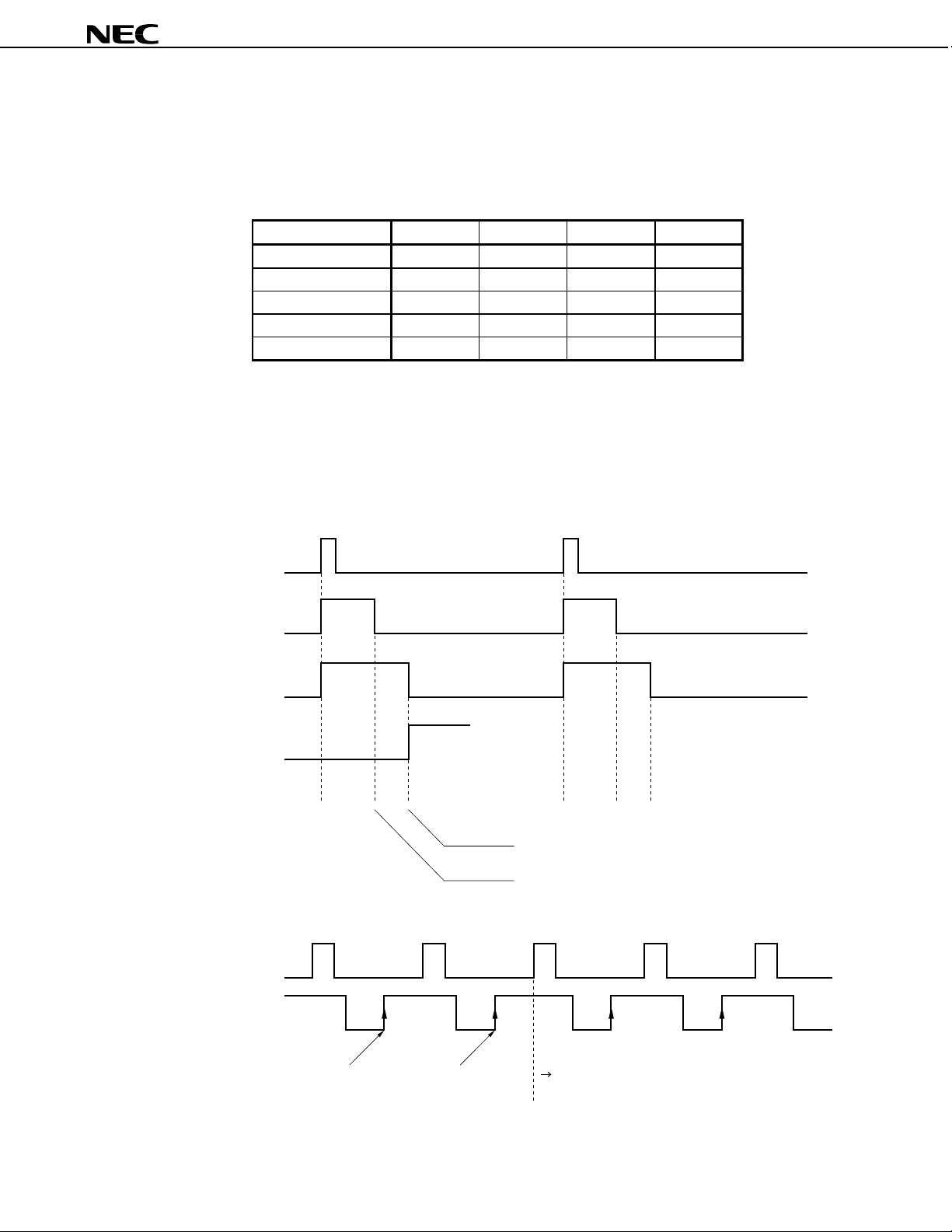
(Data Update Timing)
The standard data (pulse width, number of pulses, rotation direction, current setting, and ENABLE) of this product
are set and updated at the following latch timing.
Table 5-14. Data Update Timing
ENABLE change 1 → 10 → 11 → 00 → 0
Pulse width FF2↓ FF2↓ FF2↓−
Number of pulses FF2↓ FF2↓ FF2↓−
Rotation direction FF2↓ FF2↓ FF2↓−
Current setting FF2↓ FF1↓ FF2↓−
ENABLE FF2↓ FF1↓ FF2↓−
The timing at which data is to be updated differs, as shown in Table 5-14, depending on the enabled status.
For example, suppose the enable signal is currently “0” (output high impedance) and “1” (output conduction) is
input by the next data. In this case, the pulse width, number of pulses, and rotation direction signals are updated at
FF2(upon the completion of start up wait), and the current setting and ENABLE signals are updated at FF1 (upon
completion of start up drive wait).
Start up wait
FF1
FF2
Start up wait +
start up drive wait
Pulse output
V
D
Pulse width, number of pulses, and rotation direction
are updated.
Current setting and ENABLE are updated
(ENABLE change: 0 to 1).
V
D
(1)
(2)
(3)
LATCH I1
Initial data
identification
S1
Standard data
identification
Data Sheet S15974EJ1V0DS
S2
I1 data is output.
FF1, FF2 output
S3
19
(1) (2) (3)
µµµµ
PD16878
Pulse width Internal data retained.
Output reset
Rotation direction Internal output retained Not output
Number of pulses Internal data retained.
Output reset
Current setting Internal output retained Not output
ENABLE Internal output retained Not output
Not output
Not output
The initial mode of this product is as follows.
The IC operation can be initialized as follows:
(1) Turns ON VDD.
(2) Make RESET input “L”.
(3) Input serial initial data.
In initial mode, the operating status of the IC is as shown in Table 5-15.
Table 5-15. Operations in Initial Mode
Updated to S2 data at FF2
Updated to S2 data at either FF1 or FF2
by enable data of (2)
Item Specifications
Current consumption 100 µA
OSC Oscillation stops.
Input of external clock is inhibited.
V
D
FF1 to FF7 “L” level
PULSE OUT “L” level
EXP0 to EXP3 Undefined in the case of (1) above.
Serial operation Can be accessed after initialization in the case of (1) above.
Input inhibited.
Previous value is retained in the case of (2) above.
Can be updated by serial data in the case of (3) above.
Can be accessed after RESET has gone “H” in the case of (2) above.
Can be accessed in the case of (3) above.
Step pulse output is inhibited and FF7 is made “L” if the following conditions are satisfied.
(1) If the set number of pulses (2nd/5th: standard data) is 00H.
(2) If the checksum value is other than 00H.
(3) If the start up wait time is set to 1 VD or longer.
(4) If the start up wait time + start up drive wait time is set to 1 VD or longer.
(5) If start up wait is completed earlier than LATCH (↑).
(6) If VD is not input.
20
Data Sheet S15974EJ1V0DS

µµµµ
PD16878
Cautions on Correct Use
(1) With this product, input the data for start up wait and start up drive wait. Because the standard data are
set or updated by these wait times, if the start up wait time and start up drive wait time are not input, the
data are not updated.
(2) The start up wait time must be longer than LATCH.
(3) If the rising of the start up drive wait time is the same as the falling of the last output pulse, a count error
occurs, and the IC may malfunction.
(4) Input the initial data in a manner that it does not straddle the video sync signal (VD). If it does, the initial
data is not latched.
(5) Transmit the standard data during the start up wait time (FF1). If it is input at any other time, the data
may
not be transmitted correctly.
(6) If the LGND potential is undefined, the data may not be input correctly. Keep the LGND potential to the
minimum level. It is recommended that LGND and PGND be divided for connection (single ground) to
prevent the leakage of noise from the output circuit.
Data Sheet S15974EJ1V0DS
21
µµµµ
PD16878
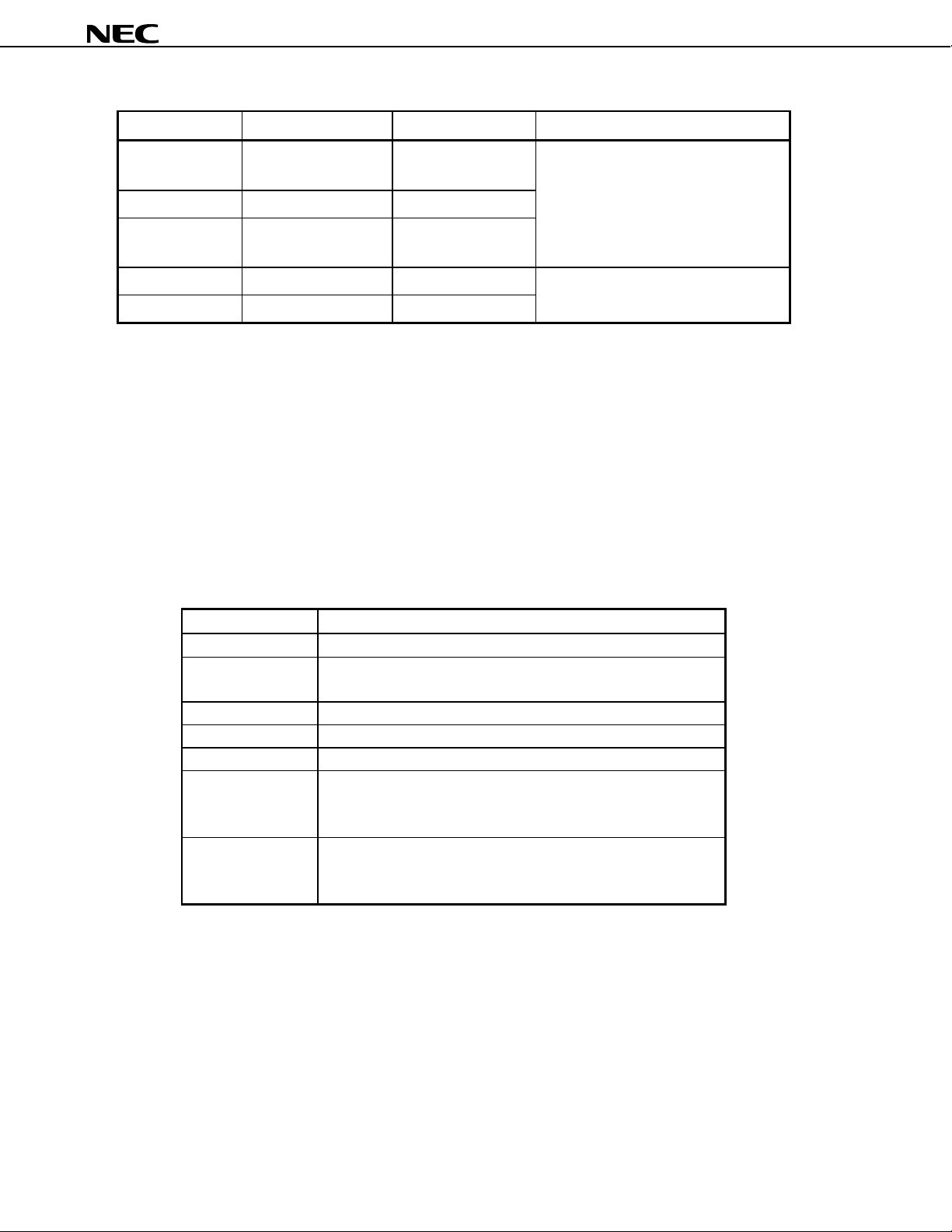
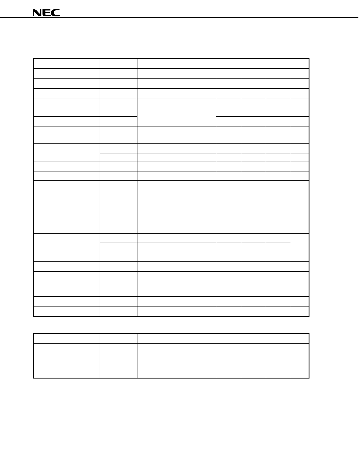
6. ELECTRICAL SPECIFICATIONS
Absolute Maximum Ratings (TA = 25°C)
Parameter Symbol Condition Rating Unit
V
DD
V
M
Input voltage V
Reference voltage V
H bridge drive current
Note 1
Instantaneous H bridge drive
Note 1
current
Power consumption
Note 2
Peak junction temperature T
Storage temperature T
IN
REF
I
M(DC)
I
M(pulse)
P
T
CH(MAX.)
stg
DC ±150 mA/phase
PW ≤ 10 ms, Duty ≤ 5% ±300 mA/phase
Notes 1. Permissible current per phase with the IC mounted on a PCB.
2. When the IC is mounted on a glass epoxy PCB (10 cm x 10 cm x 1 mm).
Caution If the absolute maximum rating of even one of the above parameters is exceeded even
momentarily, the quality of the product may be degraded. Absolute maximum ratings, therefore,
specify the values exceeding which the product may be physically damaged. Be sure to use the
product within the range of the absolute maximum ratings.
–0.5 to +6.0 VSupply voltage
–0.5 to +11.2 V
–0.5 to VDD+ 0.5 V
500 mV
1.0 W
150 °C
–55 to +150 °C
Recommended Operating Range
Parameter Symbol MIN. TYP. MAX. Unit
V
DD
V
M
Input voltage V
Reference voltage V
EXP pin input voltage V
EXP pin input current I
H bridge drive current I
H bridge drive current I
Clock frequency (OSCIN)f
Clock frequency amplitude
Serial clock frequency (SCLK) f
Video sync signal width PW
LATCH signal wait time t
SCLK wait time t
SDATA setup time t
SDATA hold time t
Chopping frequency f
Reset signal pulse width t
Operating temperature T
Peak junction temperature T
IN
REF
EXPIN
EXPIN
M(DC)
Note 1
M(pulse)
Note 2
CLK
Note 2
fCLK
V
SCLK
Note 3
(VD)
(VD-LATCH)
(SCLK-LATCH)
Note 4
setup
Note 4
hold
Note 3
OSC
RST
A
CH(MAX.)
Note 4
Note 4
2.7 5.5 VSupply voltage
4.8 11 V
0V
225 250 275 mV
−100 +100 mA
−200 +200 mA
3.9 4 5.0 MHz
0.7 V
DD
250 ns
400 ns
400 ns
80 ns
80 ns
32 124 kHz
100
−10 +85 °C
Notes 1. PW ≤ 10 ms, duty ≤ 5%
2. COSC
3. f
CLK
= 33 pF, V
= 4 MHz
= 250 mV
REF
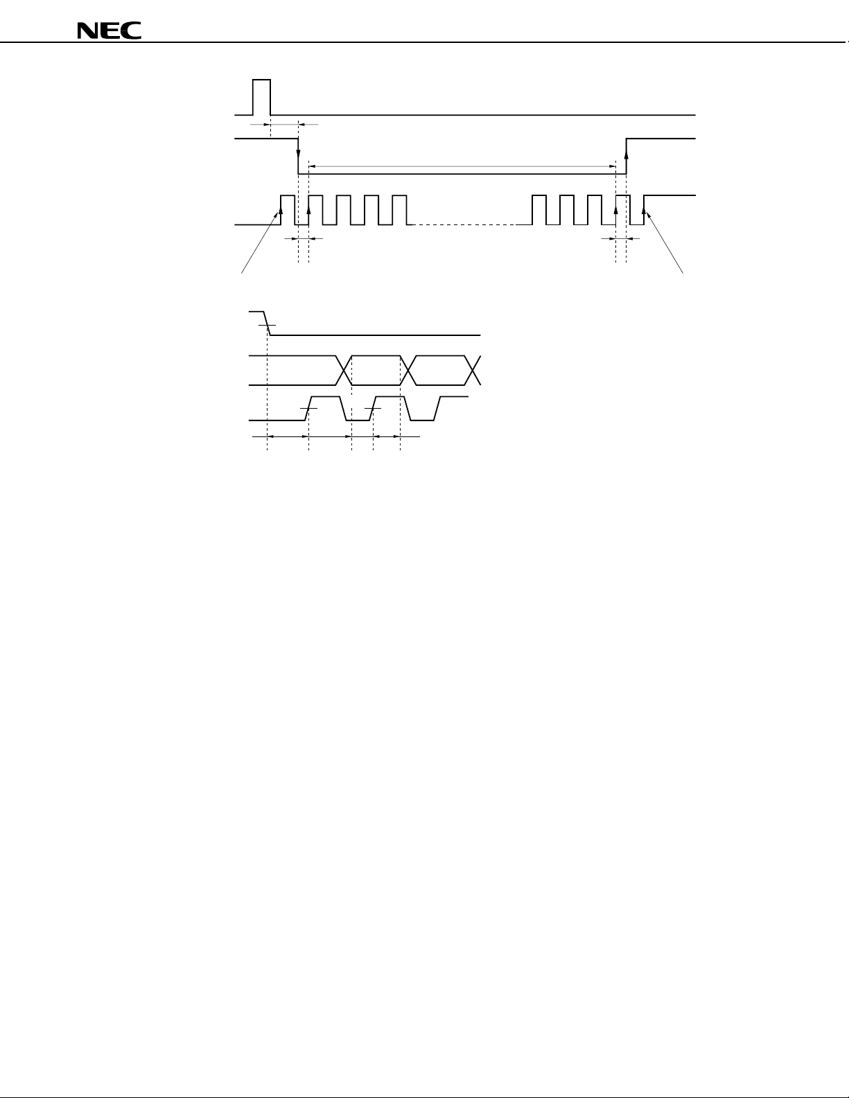
4. Serial data delay time(see the figure on the next page.)
+ 0.4 V
DD
V
DD
100
V
DD
5.0 MHz
125 °C
V
A
µ
V
s
µ
22
Data Sheet S15974EJ1V0DS
µµµµ
PD16878
V
D
(VD-LATCH)
t
LATCH
SCLK
t
(SCLK-LATCH)
Ignored because LATCH is at H level. Ignored because LATCH is at H level.
LATCH
SDATA D1 D2 D3
SCLK
50%
50% 50%
t
(SCLK-LATCH)
t
setupthold
64 clocks (8 bits x 8 bytes)
t
(SCLK-LATCH)
Data Sheet S15974EJ1V0DS
23
µµµµ
PD16878
ELECTRICAL CHARACTERISTICS
DC Characteristics (Unless otherwise specified, VDD = 3.3 V, VM = 6.0 V, VREF = 250 mV, TA = 25°C, fCLK = 4 MHz,
COSC = 33 pF, CFIL = 1000 pF, EVR = 100 mV (0000))
Parameter Symbol Condition MIN. TYP. MAX. Unit
Off VM pin current I
V
pin current I
DD
V
pin current I
DD
High level input voltage V
Low level input voltage V
Input hysteresis voltage V
α, β
)
(EXT
(EXP0 to EXP3 : open drain)
High level input current I
Low level input current I
Reset pin high level input
current
Reset pin low level input
current
Input pull down resistor R
H bridge ON resistance
oscillation: C
OSC
Note 1
= 100 pF)
MO(RESET)
DD
DD(RESET)
IH
IL
H
V
OM α (H)
V
OM α (L)
V
OEXP(H)
VOEXP(L)
IH
IL
I
IH(RST)
I
IL(RST)
IND
R
ON
f
OSC(1)
OSC(2)
f
, V
, V
No load, reset period 1.0
Output open
3.0 mA
Reset period 100
LATCH, SCLK, SDATA, VD,
RESET, OSC
IN
0.7 V
DD
0.3 V
DD
A
µ
A
µ
V
V
300 mV
5th byte 0.9 V
OM β (H)
5th byte 0.1 V
OM β (L)
Pull up (VDD)V
I
= 100 µA 0.1 V
OEXP
VIN = V
DD
DD
DD
0.06 mA
VIN = 0 V −1.0
V
= V
RST
DD
V
= 0 −1.0
RST
LATCH, SCLK, SDATA, V
D
50 200 kΩ
1.0
VMonitor output voltage 1
V
DD
VMonitor output voltage 2
V
DD
A
µ
A
µ
A
µ
IM = 100 mA 3.5 5.0 Ω
DATA: 00000 (4th byte) 0Chopping frequency (internal
kHz
DATA: 11111 (4th byte) 100 124 150
Step frequency f
VD delay time
Note 2
Sine wave peak output
Note 3
current
FIL pin voltage
FIL pin step voltage
Note 4
Note 4
STEP
VD
∆t
I
M
V
EVR
V
EVRSTEP
Minimum step 4 kHz
L = 25 mH/R = 100 Ω (1 kHz)
52 mA
EVR = 200 mV (1010)
= 6.8 Ω, f
S
R
OSC
= 64 kHz
EVR = 200 mV (1010) 370 400 430 mV
Minimum step 20 mV
AC Characteristics (Unless otherwise specified, VDD = 3.3 V, VM = 6.0 V, TA = 25°C, fCLK = 4 MHz)
Parameter Symbol Condition MIN. TYP. MAX. Unit
H bridge output circuit turn on
t
ONH
IM = 100 mA
Note 5
1.0 2.0
time
H bridge output circuit turn off
t
OFFH
IM = 100 mA
Note 5
1.0 2.0
time
Notes 1. Total of ON resistance at top and bottom of output H bridge
2. By OSCIN
and VD sync circuit
3. FB pin is monitored.
4. FIL pin is monitored. A voltage about twice that of the EVR value is output to the FIL pin.
5. 10 to 90% of the pulse peak value without filter capacitor (C
FIL
)
250 ns
s
µ
s
µ
24
Data Sheet S15974EJ1V0DS
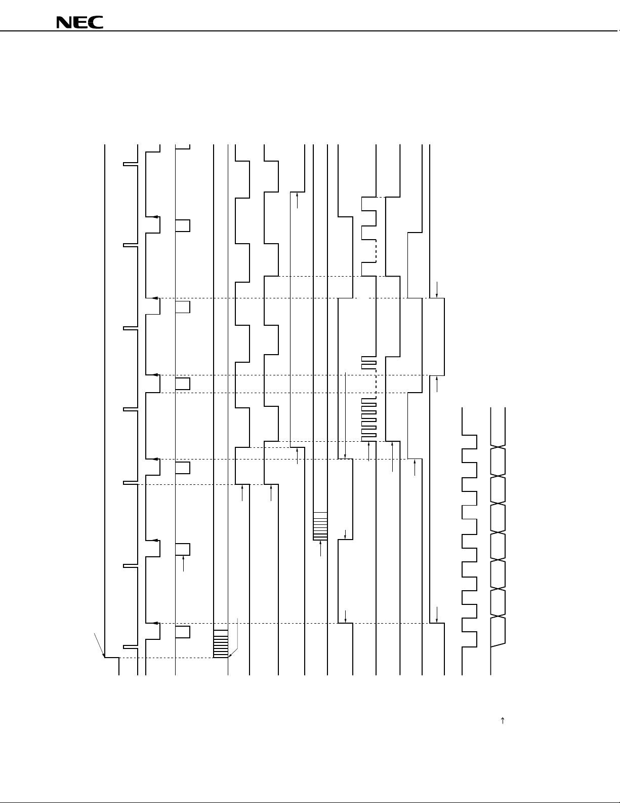
TIMING CHART (1)
5
S
Standard
EXP : 0
ENABLE: 1
Standard
4
S
EXP : 1
ENABLE: 0
Output by S5
data setting
4DATA output
S
µµµµ
PD16878
Restore to high level because
data is normal.
Initialization
EXP : 1
error DATA
Standard
3
S
EXP : 1
ENABLE: 1
Standard
2
S
1
S
Standard
Dummy data
1
I
Initial
ENABLE: 0
EXP: 1 EXP : 0
Output by
Output by
Input at rising
I1 data
I1 data
edge of RESET
Output by S2
data setting
Output by chopping
setting of I1 data
Pulse error Enable
Output by EXP
setting of S2DATA
2DATA output
S
Output by EXP
setting of S1 data
Output by EXP
setting of I1 data
to high, and at the falling edge of FF2 when the level changes from high
to low.
No pulse output because
data is erroneous
Notes 1. ENABLE is set at the falling edge of FF1 when the level changes from low
Low level because
data is abnormal.
Outputs high level while
pulse is being generated
High level because
data is normal.
Outputs high level for standard data while a
pulse output signal exists (LATCH cycle)
of a pulse in the standard data, is updated at the rising edge of LATCH
and reset once at the falling edge of LATCH. If CHECK SUM is other than
“00H”, FF7 goes low, inhibiting pulse output, even if a pulse is generated.
2. FF7 is an output signal that is used to check for the presence or absence
D0 D7D6D5D4D3D2D1
(LSB)
3. CHECK SUM output is updated at the rising edge of LATCH.
RESET
D
V
LATCH
DATA
OUT
OSC
(FF1)
Start point wait
(original oscillation)
Start point wait +
Note 1
(FF2)
EXP0 to EXP3
Chopping pulse
ENABLE OUT
start point drive wait
Data Sheet S15974EJ1V0DS
(FF3)
PULSE OUT
PULSE GATE
Note 3
Note 2
(FF7)
CHECK SUM
PULSE CHECK
SCLK
Data is held at rising edge of SCLK.
SDATA
1st byte 8th byte
25

TIMING CHART (2)
CLK
(PULSE OUT)
MOB
(CW mode)
µµµµ
PD16878
H bridge ,
1ch output status
2ch output status
α β
α β
H bridge ,
PULSE OUT
Position No. 1 2 3
H bridge
1ch output status
Current direction: A1 A2
Current direction: B2 B1
(Expanded view)
CW mode CCW mode CW mode
CLK
CW
Note1
4565
CCW
CW
Current direction: B1 B2
4323
4
CCW
CW
Current direction: A2 A1
Current direction: B2 B1
Note1Note2
CW
H bridge
2ch output status
CW
CCW
CW
CCW
Notes1. : Position No. is incremented.
In CW mode
2.
In CCW mode
: Position No. is decremented.
Remarks 1. The current value of the actual wave is approximated to the value shown on the next page.
2. The C1
, C2, D1, and D2 pins of β channel correspond to the A1, A2, B1, and B2 pins of α channel.
3. The CW mode is set if the D7 bit of the 2nd and 5th bytes of the standard data is “0”.
4. The CCW mode is set if the D7 bit of the 2nd and 5th bytes of the standard data is “1”.
26
Data Sheet S15974EJ1V0DS

RELATION BETWEEN ROTATION ANGLE, PHASE CURRENT, AND VECTOR QUANTITY
(64-DIVISION MICRO STEP)
µµµµ
PD16878
(Values of
00− 0 −−100 − 100
θ
1 5.6 2.5 9.8 17.0 − 100 − 100.48
θ
2 11.3 12.4 19.5 26.5 93.2 98.1 103 100
θ
3 16.9 22.1 29.1 36.1 90.7 95.7 100.7 100.02
θ
4 22.5 31.3 38.3 45.3 87.4 92.4 97.4 100.02
θ
5 28.1 40.1 47.1 54.1 83.2 88.2 93.2 99.99
θ
6 33.8 48.6 55.6 62.6 78.1 83.1 88.1 99.98
θ
7 39.4 58.4 63.4 68.4 72.3 77.3 82.3 99.97
θ
8 45 65.7 70.7 75.7 65.7 70.7 75.7 99.98
θ
9 50.6 72.3 77.3 82.3 58.4 63.4 68.4 99.97
θ
10 56.3 78.1 83.1 88.1 48.6 55.6 62.6 99.98
θ
11 61.9 83.2 88.2 93.2 40.1 47.1 54.1 99.99
θ
12 67.5 87.4 92.4 97.4 31.3 38.3 45.3 100.02
θ
13 73.1 90.7 95.7 100.7 22.1 29.1 36.1 100.02
θ
14 78.8 93.2 98.1 103 12.4 19.5 26.5 100
θ
15 84.4 − 100 − 2.5 9.8 17.0 100.48
θ
16 90 − 100 −−0 − 100
θ
µµµµ
PD16878 for reference)
Step Rotation angle (
θ
) A phase current B phase current Vector quantity
MIN. TYP. MAX. MIN. TYP. MAX. TYP.
Remark These data do not indicate guaranteed values.
Data Sheet S15974EJ1V0DS
27

7. PACKAGE DRAWING
38-PIN PLASTIC SSOP (7.62 mm (300))
38 20
detail of lead end
F
G
µµµµ
PD16878
119
A
P
E
H
I
S
C
D
M
M
N
S
NOTE
Each lead centerline is located within 0.10 mm of
its true position (T.P.) at maximum material condition.
B
K
L
ITEM
MILLIMETERS
A
B
C
D
E
F
G
H
I
J
K
L
M
N
P
P38GS-65-BGG-1
J
12.7±0.3
0.65 MAX.
0.65 (T.P.)
+0.05
0.37
−0.1
0.125±0.075
1.675±0.125
1.55
7.7±0.2
5.6±0.2
1.05±0.2
+0.1
0.2
−0.05
0.6±0.2
0.10
0.10
+7°
3°
−3°
28
Data Sheet S15974EJ1V0DS

µµµµ
PD16878
8. RECOMMENDED SOLDERING CONDITIONS
When soldering this product, it is highly recommended to observe the conditions as shown below. If other
soldering processes are used, or if the soldering is performed under different conditions, please make sure to consult
with our sales offices.
For more details, refer to our document “SEMICONDUCTOR DEVICE MOUNTING TECHNOLOGY MANUAL”
(C10535E).
Type of Surface Mount Device
µµµµ
PD16878GS-BGG: 38-pin plastic shrink SOP (7.62 mm (300))
Process Soldering conditions Symbol
Infrared Ray Reflow Peak temperature: 235°C or below (Package surface temperature),
Reflow time: 30 seconds or less (at 210°C or higher),
Maximum number of reflow processes: 3 time or less,
Number of days: None
Flux: Rosin-based flux with low chlorine content (chlorine 0.2 Wt% or below) is
recommended.
Note
,
IR35-00-3
Vapor Phase Soldering Peak temperature: 215°C or below (Package surface temperature),
Reflow time: 40 seconds or less (at 200°C or higher),
Maximum number of reflow processes: 3 time or less,
Number of days: None
Flux: Rosin-based flux with low chlorine content (chlorine 0.2 Wt% or below) is
recommended.
Wave Soldering Solder temperature: 260°C or below, Flow time: 10 seconds or less,
Maximum number of flow processes: 1 time,
Pre-heating temperature: 120°C or below (Package surface temperature),
Flux: Rosin-based flux with low chlorine content (chlorine 0.2 Wt% or below) is
recommended.
Partial Heating Method Pin temperature: 300°C or below,
Heat time: 3 seconds or less (Per each side of the device).
Note
,
VP15-00-3
WS60-00-1
−
Note Number of days the device can be stored after the dry pack has been opened, at conditions of 25°C, 65%RH.
Caution Apply only one kind of soldering condition to a device, except for “partial heating method”, or the
device will be damaged by heat stress.
Data Sheet S15974EJ1V0DS
29

[MEMO]
µµµµ
PD16878
30
Data Sheet S15974EJ1V0DS

NOTES FOR CMOS DEVICES
1 PRECAUTION AGAINST ESD FOR SEMICONDUCTORS
Note:
Strong electric field, when exposed to a MOS device, can cause destruction of the gate oxide and
ultimately degrade the device operation. Steps must be taken to stop generation of static electricity
as much as possible, and quickly dissipate it once, when it has occurred. Environmental control
must be adequate. When it is dry, humidifier should be used. It is recommended to avoid using
insulators that easily build static electricity. Semiconductor devices must be stored and transported
in an anti-static container, static shielding bag or conductive material. All test and measurement
tools including work bench and floor should be grounded. The operator should be grounded using
wrist strap. Semiconductor devices must not be touched with bare hands. Similar precautions need
to be taken for PW boards with semiconductor devices on it.
2 HANDLING OF UNUSED INPUT PINS FOR CMOS
Note:
No connection for CMOS device inputs can be cause of malfunction. If no connection is provided
to the input pins, it is possible that an internal input level may be generated due to noise, etc., hence
causing malfunction. CMOS devices behave differently than Bipolar or NMOS devices. Input levels
of CMOS devices must be fixed high or low by using a pull-up or pull-down circuitry. Each unused
DD
pin should be connected to V
being an output pin. All handling related to the unused pins must be judged device by device and
related specifications governing the devices.
or GND with a resistor, if it is considered to have a possibility of
µµµµ
PD16878
3 STATUS BEFORE INITIALIZATION OF MOS DEVICES
Note:
Power-on does not necessarily define initial status of MOS device. Production process of MOS
does not define the initial operation status of the device. Immediately after the power source is
turned ON, the devices with reset function have not yet been initialized. Hence, power-on does
not guarantee out-pin levels, I/O settings or contents of registers. Device is not initialized until the
reset signal is received. Reset operation must be executed immediately after power-on for devices
having reset function.
Data Sheet S15974EJ1V0DS
31

µµµµ
PD16878
•
The information in this document is current as of January, 2002. The information is subject to
change without notice. For actual design-in, refer to the latest publications of NEC's data sheets or
data books, etc., for the most up-to-date specifications of NEC semiconductor products. Not all
products and/or types are available in every country. Please check with an NEC sales representative
for availability and additional information.
•
No part of this document may be copied or reproduced in any form or by any means without prior
written consent of NEC. NEC assumes no responsibility for any errors that may appear in this document.
•
NEC does not assume any liability for infringement of patents, copyrights or other intellectual property rights of
third parties by or arising from the use of NEC semiconductor products listed in this document or any other
liability arising from the use of such products. No license, express, implied or otherwise, is granted under any
patents, copyrights or other intellectual property rights of NEC or others.
•
Descriptions of circuits, software and other related information in this document are provided for illustrative
purposes in semiconductor product operation and application examples. The incorporation of these
circuits, software and information in the design of customer's equipment shall be done under the full
responsibility of customer. NEC assumes no responsibility for any losses incurred by customers or third
parties arising from the use of these circuits, software and information.
•
While NEC endeavours to enhance the quality, reliability and safety of NEC semiconductor products, customers
agree and acknowledge that the possibility of defects thereof cannot be eliminated entirely. To minimize
risks of damage to property or injury (including death) to persons arising from defects in NEC
semiconductor products, customers must incorporate sufficient safety measures in their design, such as
redundancy, fire-containment, and anti-failure features.
•
NEC semiconductor products are classified into the following three quality grades:
"Standard", "Special" and "Specific". The "Specific" quality grade applies only to semiconductor products
developed based on a customer-designated "quality assurance program" for a specific application. The
recommended applications of a semiconductor product depend on its quality grade, as indicated below.
Customers must check the quality grade of each semiconductor product before using it in a particular
application.
"Standard": Computers, office equipment, communications equipment, test and measurement equipment, audio
and visual equipment, home electronic appliances, machine tools, personal electronic equipment
and industrial robots
"Special": Transportation equipment (automobiles, trains, ships, etc.), traffic control systems, anti-disaster
systems, anti-crime systems, safety equipment and medical equipment (not specifically designed
for life support)
"Specific": Aircraft, aerospace equipment, submersible repeaters, nuclear reactor control systems, life
support systems and medical equipment for life support, etc.
The quality grade of NEC semiconductor products is "Standard" unless otherwise expressly specified in NEC's
data sheets or data books, etc. If customers wish to use NEC semiconductor products in applications not
intended by NEC, they must contact an NEC sales representative in advance to determine NEC's willingness
to support a given application.
(Note)
(1) "NEC" as used in this statement means NEC Corporation and also includes its majority-owned subsidiaries.
(2) "NEC semiconductor products" means any semiconductor product developed or manufactured by or for
NEC (as defined above).
M8E 00. 4
 Loading...