NEC UPD16877MA-6A5 Datasheet

DATA SHEET
MOS INTEGRATED CIRCUIT
µµµµ
PD16877
MONOLITHIC QUAD H-BRIDGE DRIVER CIRCUIT
DESCRIPTION
The µPD16877 is monolithic quad H-bridge driver LSI which uses power MOSFETs in the output stages. By using
the MOS process, this driver IC has substantially improved saturation voltage and power consumption as compared
with conventional driver circuits using bipolar transistors.
By eliminating the charge pump circuit, the current during power-OFF is drastically decreased.
In addition, a low-voltage malfunction prevention circuit is also provided that prevents the IC from malfunctioning
when the supply voltage drops.
As the package, a 24-pin plastic TSSOP is adopted to enable the creation of compact, slim application sets.
This driver IC can drive two stepping motor at the same time, and is ideal for driving stepping motors in the lens of
a camcorder.
FEATURES
Four H bridge circuits employing power MOSFETs
Low current consumption by eliminating charge pump
VM pin current when power-OFF: 10 µA MAX. VDD pin current: 10 µA MAX.
Input logic frequency: 100 kHz
3-V power supply
Minimum operating supply voltage: 2.5 V
Low voltage malfunction prevention circuit
24-pin plastic TSSOP (5.72 mm (225))
ORDERING INFORMATION
Part Number Package
µ
PD16877MA-6A5 24-pin plastic TSSOP (5.72 mm (225))
The information in this document is subject to change without notice. Before using this document, please
confirm that this is the latest version.
Not all devices/types available in every country. Please check with local NEC representative for
availability and additional information.
Document No. S13964EJ1V0DS00 (1st edition)
Date Published March 2000 N CP(K)
Printed in Japan
©
2000

µµµµ
PD16877
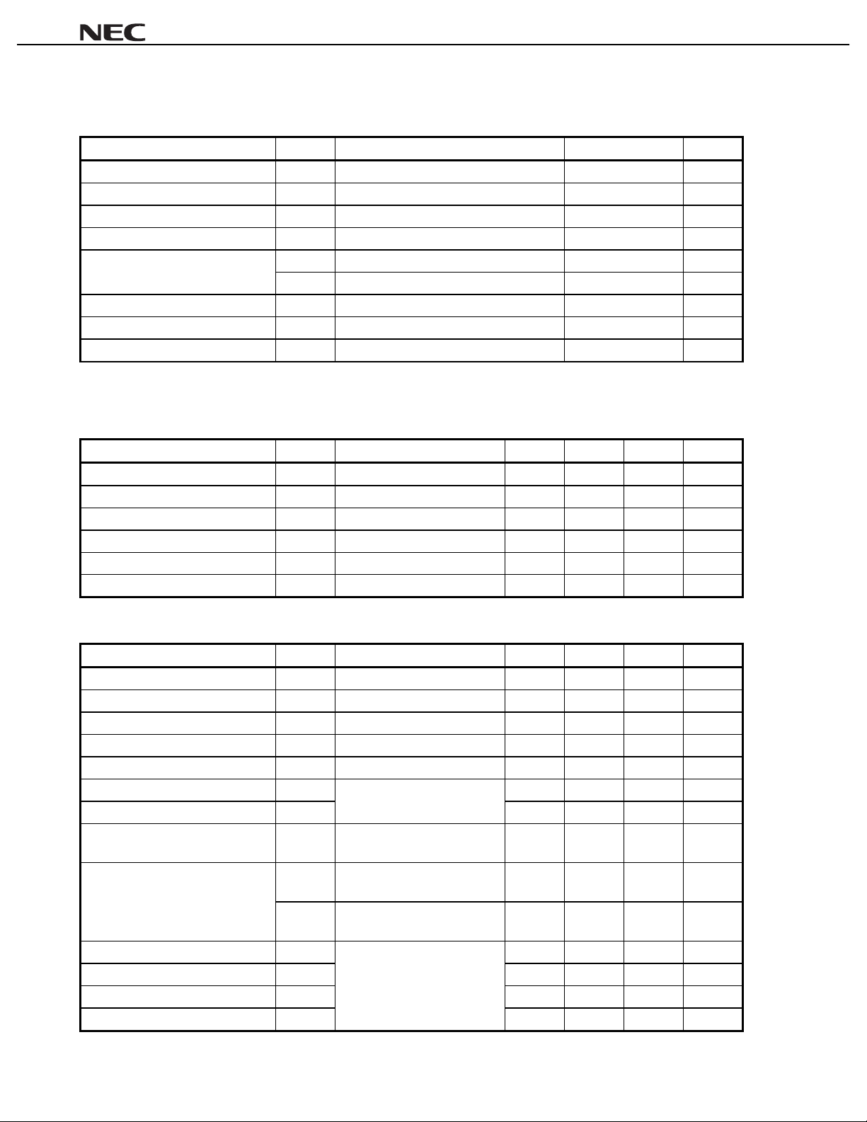
ABSOLUTE MAXIMUM RATINGS (TA = 25
When mounted on a glass epoxy board (10 cm
C)
°°°°
××××
Parameter Symbol Condition Rating Unit
Control block supply v ol t age V
Output block supply v ol tage V
Input voltage V
Output terminal voltage V
Output current
Power consumption P
Peak junction temperature T
Storage temperature range T
DD
M
IN
OUT
D(DC)
I
D(pulse)
I
T
CH(MAX)
stg
DC
PW ≤ 10 ms, Duty ≤ 5%
RECOMMENDED OPERATING CONDITIONS
When mounted on a glass epoxy board (10 cm
Parameter Symbol Condition MIN. TYP. MAX. Unit
Control block supply v ol t age V
Output block supply v ol tage V
Output current I
Operating frequency f
Operating temperature range T
Peak junction temperature T
DD
M
D(DC)
IN
A
CH(MAX)
××××
DC
IN, EN terminal 100 kHz
10 cm
10 cm
1 mm, 15% copper foil)
××××
1 mm, 15% copper foil)
××××
2.5 5.5 V
2.7 5.5 V
0.2 +0.2 A
−
10 85
−
0.5 to +6.0 V
−
0.5 to +6.0 V
−
DD
0.5 to V
−
+ 0.5 V
6.2 V
0.3 A/ch
±
0.7 A/ch
±
0.7 W
150
55 to +150
−
125
C
°
C
°
C
°
C
°
CHARACTERISTICS (Unless otherwise specified, VDD = VM = 3 V, TA = 25
Parameter Symbol Condition MIN. TYP. MAX. Unit
Off state VM pin current I
VDD pin current I
High level input current I
Low level input current I
Input pull down resistance R
High level input voltage V
Low level input voltage V
H-bridge ON resistance R
Low voltage malfunction
prevention circuit operati ng voltage
H bridge output turn-on time t
H bridge output turn-off time t
H bridge output rise time t
H bridge output fall time t
M(OFF)
DD
IH
IL
IND
IH
IL
ON
DDS1
V
DDS2
V
ONH
OFFH
r
f
All control terminal: L l evel 10
All control terminal: L l evel 10
DD
VIN = V
VIN = 0 V
1.0
−
50 200 k
DD
2.5 V ≤ VDD ≤ 5.5 V
0.7 × V
3.0 0.3 × V
−
2.5 V ≤ VM, VDD ≤ 5.5 V
Upper + lower
VM = 5 V
−10°C ≤
VM = 3 V
−10°C ≤
RM = 20
Figure 1
A
T
≤ +85°C
A
T
≤ +85°C
Ω
0.8 2.5 V
0.65 2.5 V
0.1 0.4 1.0
C)
°°°°
0.06 mA
VDD+0.3 V
3.0
0.7 20
0.2 0. 5
70 200 ns
A
µ
A
µ
A
µ
Ω
DD
V
Ω
s
µ
s
µ
s
µ
2
Data Sheet S13964EJ1V0DS00

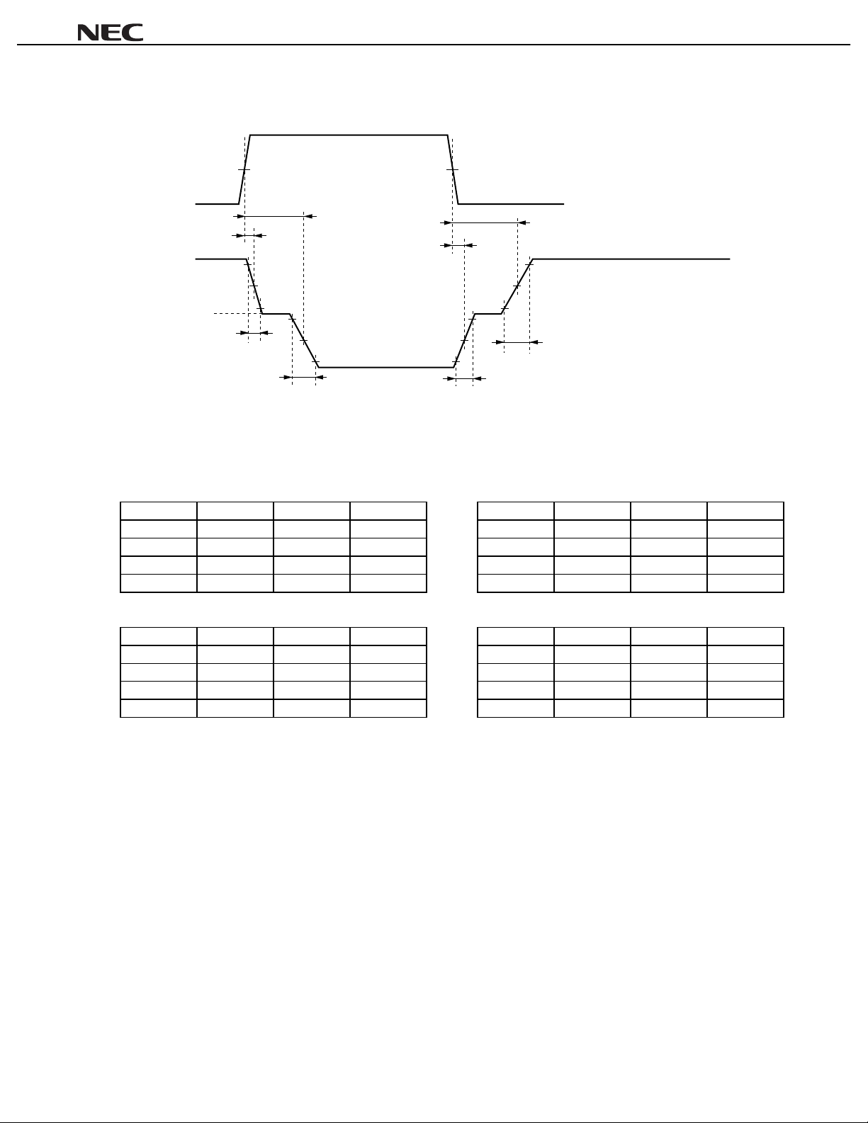
Figure 1. Switching time condition
100%
µµµµ
PD16877
50%
V
IN
50%
0%
t
ONH
t
OFFH
t
OFFH
t
ONH
100% 100%
90% 90%
50%
I
D
0%
t
10% 10%
−10%
f
−50% −50%
−90% −90%
t
r
−100%
50%
−10%
t
r
t
f
The current flowing in the direction from
A
to OUT_B is assumed to be (+).
OUT_
FUNCTION TABLE
Channel 1 Channel 2
1
EN
HLHL HLHL
HHLH HHLH
LLZZ LLZZ
LHZZ LHZZ
IN
1
OUT
1A
OUT
1B
EN
2
IN
2
OUT
2A
OUT
2B
Channel 3 Channel 4
3
EN
HLHL HLHL
HHLH HHLH
LLZZ LLZZ
LHZZ LHZZ
IN
3
OUT
3A
OUT
3B
EN
4
IN
4
OUT
4A
OUT
H: High-level, L: Low-level, Z: High impedance
4B
Data Sheet S13964EJ1V0DS00
3

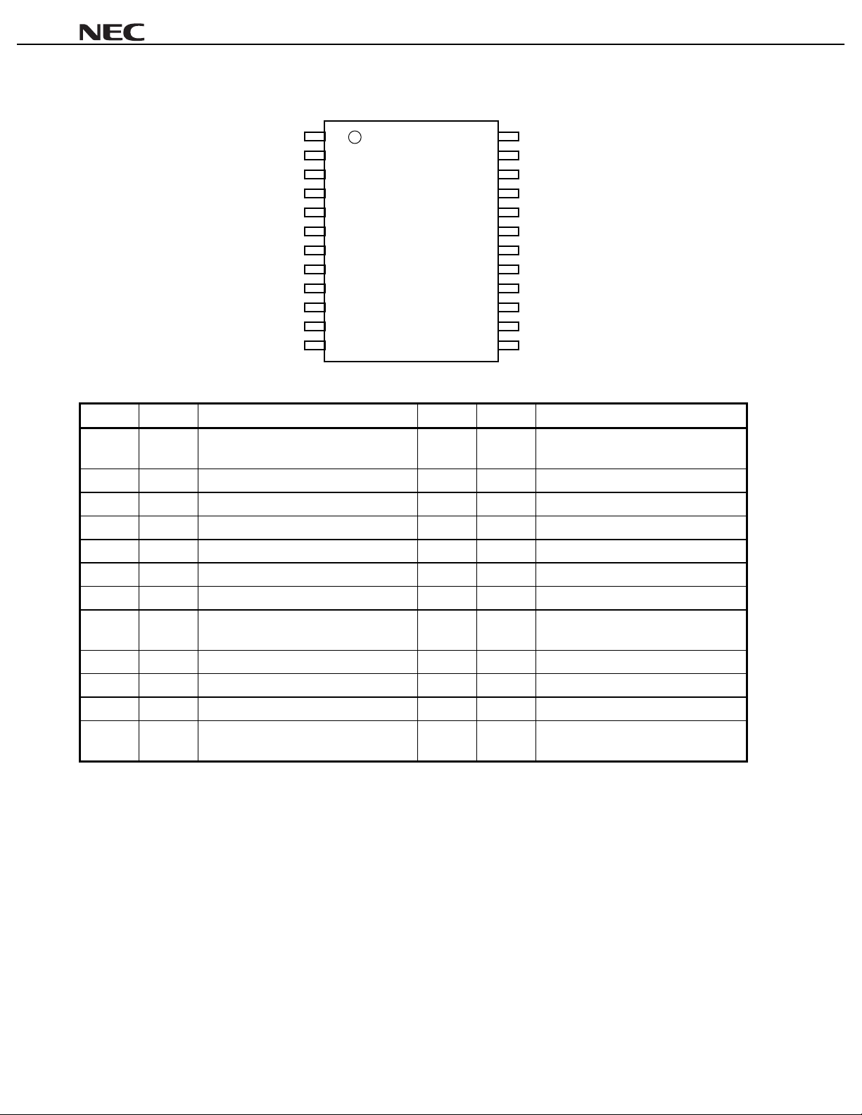
PIN CONNECTION
µµµµ
PD16877
V
OUT
PGND
OUT
OUT
PGND
OUT
V
IN
EN
IN
EN
M1
1
1A
2
3
2A
4
3A
5
6
4A
7
M4
8
1
9
1
10
2
11
2
12
24
23
22
21
20
19
18
17
16
15
14
13
V
DD
OUT
PGND
OUT
V
M23
OUT
PGND
OUT
EN
4
IN
4
EN
3
IN
3
1B
2B
3B
4B
Pin No. Pin name Pin function Pin No. Pin name Pin function
Output block supply v ol tage input
1V
M1
terminal
13 IN
2OUT1AOutput terminal 14 EN
3 PGND Ground terminal 15 IN
4OUT2AOutput terminal 16 EN
5OUT3AOutput terminal 17 OUT
3
Control terminal (channel 3)
3
Enable terminal (channel 3)
4
Control terminal (channel 4)
4
Enable terminal (channel 4)
4B
Output terminal
6 PGND Ground terminal 18 PGND Ground terminal
7OUT4AOutput terminal 19 OUT
Output block supply v ol tage input
8V
M4
terminal
20 V
9IN1Control terminal (channel 1) 21 OUT
10 EN
11 IN
12 EN
1
Enable terminal (channel 1) 22 PGND Ground terminal
2
Control terminal (channel 2) 23 OUT
2
Enable terminal (channel 2) 24 V
3B
Output terminal
Output block supply v ol tage input
M23
terminal
2B
Output terminal
1B
Output terminal
Control block supply v ol t age i nput
DD
terminal
4
Data Sheet S13964EJ1V0DS00
 Loading...