NEC PS8601, PS8601L Datasheet

DATA SHEET
DATA SHEET
PHOTOCOUPLERS
PS8601, PS8601L
HIGH SPEED ANALOG OUTPUT TYPE
8 PIN PHOTOCOUPLER
DESCRIPTION
PS8601 and PS8601L is a 8-pin high speed photocoupler containing a GaAIAs LED on input side and a P-N
photodiode and a high speed amplifier transistor on output side on one chip. PS8601 is in a plastic DIP (Dual In-line
Package). PS8601L is lead bending type (Gull wing) for surface mount.
FEATURES
• High supply voltage (VCC = 35 V MAX.)
PHL
• High speed response (t
• High isolation voltage (BV: 5 000 V
• TTL, CMOS compatible with a resistor
• Taping product number (PS8601L-E3)
• UL recognized [File No. E72422(s)]
• VDE0884 recognized: option
PLH
, t
: 0.8 s MAX.)
r.m.s.
MIN.)
APPLICATIONS
• Interface circuit for various instrumentations, control equipments.
• Computer and peripheral manufactures.
• Electrical isolation of TV video terminals.
ORDERING INFORMATION
PART NUMBER PACKAGE SAFETY STANDARD APPROVAL
PS8601 8 pin DIP
PS8601L 8 pin DIP, lead bending type
PS8601L1
PS8601L2
PS8601-V 8 pin DIP
PS8601L-V 8 pin DIP, lead bending type
PS8601L1-V
PS8601L2-V
8 pin DIP, lead bending type
(for long distance)
8 pin DIP, lead bending type
(for long distance)
Normal specification products
• UL Approved
VDE0884 specification products (option)
• VDE Approved
[Handling Precaution]
This product is weak for static electricity by designed with high speed integrated circuit. So, protect against static
electricity when handling.
Document No. P11650EJ2V0DS00 (2nd edition)
(Previous No. LC-2362)
Date Published June 1996 P
Printed in Japan
1995©

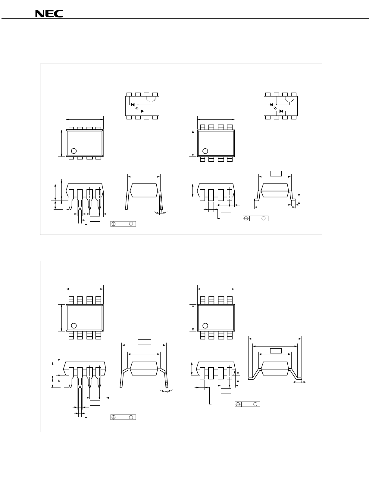
PACKAGE DIMENSIONS (Unit: mm)
DIP (Dual In-line Package) Lead Bending type (Gull-wing)
PS8601, PS8601L
PS8601
4.55
MAX.
2.8
MIN.
10.16 MAX.
85
6.5
14
3.8
MAX.
0.65
1.34
2.54
0.50 ± 0.10
PIN CONNECTIONS (Top View)
Output
8765
1234
Input
1. NC
2. Anode
3. Cathode
4. NC
5. Emitter
O
6. V
7. Base
CC
8. V
7.62
1.27
MAX.
0 to 15
M
0.25
PS8601L
PIN CONNECTIONS (Top View)
Output
8765
10.16 MAX.
85
6.5
14
3.8 MAX.
1.27
MAX.
2.54
o
1.34 ± 0.10
0.25
1. NC
2. Anode
3. Cathode
4. NC
M
1234
Input
5. Emitter
O
6. V
7. Base
CC
8. V
7.62
9.60 ± 0.4
0.05 to 0.2
0.9
± 0.25
PS8601L1
6.5
3.8
MAX.
4.25
MAX.
2.8
MIN.
10.16 MAX.
85
14
0.35
1.34
2.54
0.50 ± 0.10
1.27 MAX.
0.25
Lead Bending type (for long distance)
PS8601L2
10.16 MAX.
85
6.5
10.16
14
7.62
0.05 to 0.2
3.8 MAX.
1.27 MAX.
o
0 to 15
M
2.54
1.34 ± 0.10
0.25
11.8 ± 0.4
10.16
7.62
0.9 ± 0.25
M
2

PS8601, PS8601L
ABSOLUTE MAXIMUM RATINGS (TC = 25
C)
Diode
Forward Current I
Reverse Voltage V
Power Dissipation P
F
R
D
25 mA
5V
45 mW
Detector
Supply Voltage V
Output Voltage V
Output Current I
Power Dissipation P
Isolation Voltage
*1
Operating Temperature T
Storage Temperature T
*1
AC voltage for 1 minute at TA = 25 C, RH = 60 % between input and output.
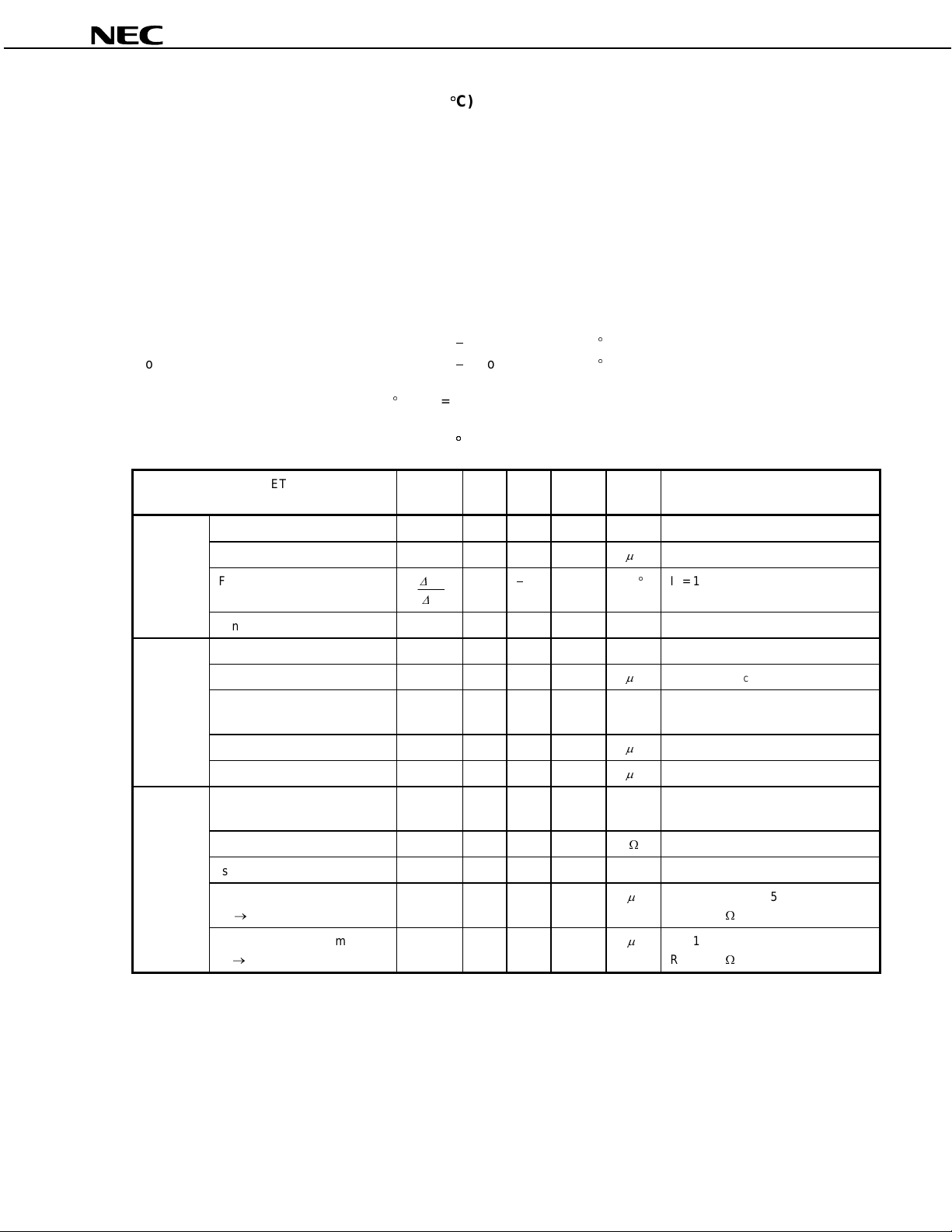
ELECTRICAL CHARACTERISTICS (TA = 25
PARAMETER SYMBOL MIN. TYP.MAX. UNIT TEST CONDITIONS
Diode Forward Voltage V
Reverse Current I
Forward Voltage Temperature
Coefficient
Junction Capacitance C
Detector High Level Output Current IOH 1 3 500 nA IF = 0 mA, VCC = VO = 5.5 V
High Level Output Current IOH 2 100
Low Level Output Voltage V
Low Level Supply Current I
High Level Supply Current I
Coupler Current Transfer Ratio CTR 15 % IF = 16 mA, VCC = 4.5 V,
Isolation Resistance R
Isolation Capacitance C
Propagation Delay Time
(H L)
Propagation Delay Time
(L H)
CC
O
O
C
35 V
35 V
8mA
100 mW
BV 5 000 V
A
stg
55 to +100
55 to +150
C)
F
R
F
V
T
t
OL
CCL
CCH
1-2
1-2
PHL
t
*2
PLH
t
*2
1.7 2.2 V IF = 16 mA
10
1.6 mV/CI
60 pF V = 0, f = 1 MHz
0.1 0.4 V IF = 16 mA, VCC = 4.5 V,
50
0.01 1
11
10
0.7 pF V = 0, f - 1 MHz
0.5 0.8
0.3 0.8
r.m.s.
C
C
AVR = 5 V
F
= 16 mA
AIF = 0 mA, VCC - VO = 35 V
O
= 1.2 mA
I
AIF = 16 mA, VO = Open, VCC = 35 V
AIF = 0 mA, VO = Open, VCC = 35 V
O
= 0.4 V
V
in-out
V
IF = 16 mA, VCC = 5 V
s
L
= 1.9 k
R
IF = 16 mA, VCC = 5 V
s
L
= 1.9 k
R
= 1 kV
DC
3
 Loading...